

TIP110, TIP111, TIP112
(NPN); TIP115, TIP116,
TIP117 (PNP)
TIP111, TIP112, TIP116, and TIP117 are Preferred Devices
Plastic Medium-Power
Complementary Silicon
Transistors
http://onsemi.com
Designed for general-purpose amplifier and low-speed switching
applications.
Features
•High DC Current Gain -
hFE= 2500 (Typ) @ IC
= 1.0 Adc
•Collector-Emitter Sustaining Voltage - @ 30 mAdc
V
CEO(sus)
= 60 Vdc (Min) - TIP110, TIP115
= 80 Vdc (Min) - TIP111, TIP116
= 100 Vdc (Min) - TIP112, TIP117
•Low Collector-Emitter Saturation Voltage -
V
= 2.5 Vdc (Max) @ IC
CE(sat)
= 2.0 Adc
•Monolithic Construction with Built-in Base-Emitter Shunt Resistors
•Pb-Free Packages are Available*
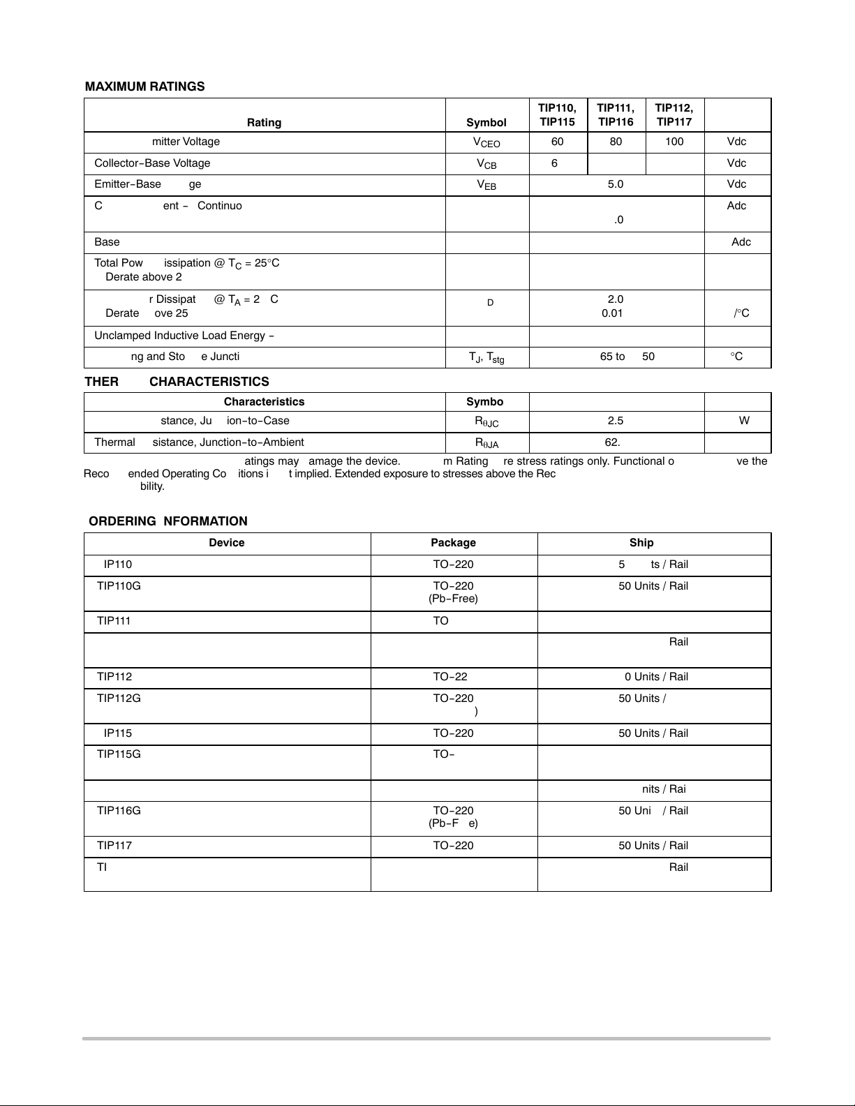
DARLINGTON
2 AMPERE
COMPLEMENTARY SILICON
POWER TRANSISTORS
60-80-100 VOLTS, 50 WATTS
MARKING
DIAGRAM
4
TO-220AB
CASE 221A
1
2
3
TIP11x = Device Code
x = 0, 1, 2, 5, 6, or 7
A = Assembly Location
Y = Year
WW = Work Week
G = Pb-Free Package
STYLE 1
TIP11xG
AYWW
*For additional information on our Pb-Free strategy and soldering details, please
download the ON Semiconductor Soldering and Mounting Techniques
Reference Manual, SOLDERRM/D.
© Semiconductor Components Industries, LLC, 2007
November, 2007 - Rev. 6
1 Publication Order Number:
See detailed ordering and shipping information in the package
ORDERING INFORMATION
dimensions section on page 2 of this data sheet.
Preferred devices are recommended choices for future use
and best overall value.
TIP110/D
TIP110, TIP111, TIP112 (NPN); TIP115, TIP116, TIP117 (PNP)
MAXIMUM RATINGS
TIP110,
TIP115
60
60
Collector-Emitter Voltage
Collector-Base Voltage
Emitter-Base Voltage
Collector Current - Continuous
Rating
Symbol
V
CEO
V
CB
V
EB
I
C
- Peak
Base Current
Total Power Dissipation @ TC = 25°C
I
B
P
D
Derate above 25°C
Total Power Dissipation @ TA = 25°C
P
D
Derate above 25°C
Unclamped Inductive Load Energy - Figure 13
Operating and Storage Junction
TJ, T
E
stg
THERMAL CHARACTERISTICS
Characteristics
Thermal Resistance, Junction-to-Case
Thermal Resistance, Junction-to-Ambient
Stresses exceeding Maximum Ratings may damage the device. Maximum Ratings are stress ratings only. Functional operation above the
Recommended Operating Conditions is not implied. Extended exposure to stresses above the Recommended Operating Conditions may affect
device reliability.
Symbol
R
q
JC
R
q
JA
TIP111,
TIP116
80
80
5.0
2.0
4.0
50
50
0.4
2.0
0.016
25
–65 to +150
Max
2.5
62.5
TIP112,
TIP117
100
100
Unit
Vdc
Vdc
Vdc
Adc
mAdc
W
W/°C
W
W/°C
mJ
°C
Unit
°C/W
°C/W
ORDERING INFORMATION
Device Package Shipping
TIP110 TO-220 50 Units / Rail
TIP110G TO-220
(Pb-Free)
TIP111 TO-220 50 Units / Rail
TIP111G TO-220
(Pb-Free)
TIP112 TO-220 50 Units / Rail
TIP112G TO-220
(Pb-Free)
TIP115 TO-220 50 Units / Rail
TIP115G TO-220
(Pb-Free)
TIP116 TO-220 50 Units / Rail
TIP116G TO-220
(Pb-Free)
TIP117 TO-220 50 Units / Rail
TIP117G TO-220
(Pb-Free)
50 Units / Rail
50 Units / Rail
50 Units / Rail
50 Units / Rail
50 Units / Rail
50 Units / Rail
http://onsemi.com
2
TIP110, TIP111, TIP112 (NPN); TIP115, TIP116, TIP117 (PNP)
ELECTRICAL CHARACTERISTICS (T
= 25°C unless otherwise noted)
C
Characteristic
OFF CHARACTERISTICS
Collector-Emitter Sustaining Voltage (Note 1)
= 30 mAdc, IB = 0) TIP110, TIP115
(I
C
TIP111, TIP116
TIP112, TIP117
Collector Cutoff Current
(VCE = 30 Vdc, IB = 0) TIP110, TIP115
(VCE = 40 Vdc, IB = 0) TIP111, TIP116
(VCE = 50 Vdc, IB = 0) TIP112 ,TIP117
Collector Cutoff Current
(VCB = 60 Vdc, IE = 0) TIP110, TIP115
(VCB = 80 Vdc, IE = 0) TIP111, TIP116
(VCB = 100 Vdc, IE = 0) TIP112, TIP117
Emitter Cutoff Current
(VBE = 5.0 Vdc, IC = 0)
ON CHARACTERISTICS (Note 1)
DC Current Gain
(IC = 1.0 Adc, VCE = 4.0 Vdc)
(IC = 2.0 Adc, VCE = 4.0 Vdc)
Collector-Emitter Saturation Voltage
(IC = 2.0 Adc, IB = 8.0 mAdc)
Base-Emitter On Voltage
(IC = 2.0 Adc, VCE = 4.0 Vdc)
DYNAMIC CHARACTERISTICS
Small-Signal Current Gain
(IC = 0.75 Adc, VCE = 10 Vdc, f = 1.0 MHz)
Output Capacitance
(VCB = 10 Vdc, IE = 0, f = 0.1 MHz) TIP115, TIP116, TIP117
TIP110, TIP111, TIP112
1. Pulse Test: Pulse Width v 300 ms, Duty Cycle v 2%.
Symbol
V
CEO(sus)
I
CEO
I
CBO
I
EBO
h
FE
V
CE(sat)
V
BE(on)
h
fe
C
ob
Min
60
80
100
-
-
-
-
-
-
-
1000
500
-
-
25
-
-
Max
-
-
-
2.0
2.0
2.0
1.0
1.0
1.0
2.0
-
-
2.5
2.8
-
200
100
Unit
Vdc
mAdc
mAdc
mAdc
-
Vdc
Vdc
-
pF
3.0
2.0
1.0
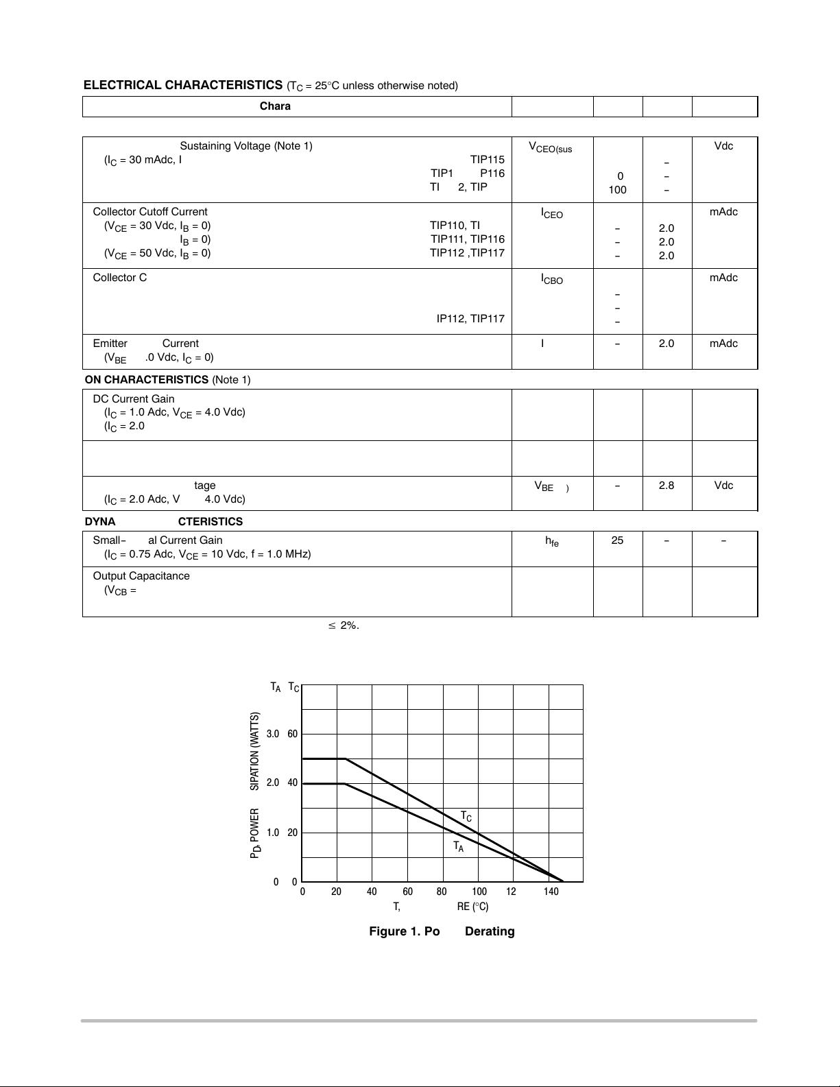
, POWER DISSIPATION (WATTS)
D
P
T
T
C
A
60
40
T
C
20
T
A
0
0
0 20 40 60 80 100 120 160
T, TEMPERATURE (°C)
Figure 1. Power Derating
http://onsemi.com
3
140

TIP110, TIP111, TIP112 (NPN); TIP115, TIP116, TIP117 (PNP)
RB & RC VARIED TO OBTAIN DESIRED CURRENT LEVELS
D
, MUST BE FAST RECOVERY TYPE, eg:
1
1N5825 USED ABOVE I
≈ 100 mA
B
MSD6100 USED BELOW IB ≈ 100 mA
V
2
approx
+8.0 V
0
V
1
approx
-12 V
, tf ≤ 10 ns
t
r
DUTY CYCLE = 1.0%
25 ms
R
B
D
1
51
for td and tr, D1 is disconnected
and V2 = 0, RB and RC are varied
to obtain desired test currents.
For NPN test circuit, reverse diode,
polarities and input pulses.
≈ 8.0 k
+4.0 V
Figure 2. Switching Times Test Circuit
1.0
0.7
D = 0.5
0.5
0.3
0.2
0.1
(NORMALIZED)
0.07
0.05
0.03
r(t), TRANSIENT THERMAL RESISTANCE
0.02
0.01
0.01
0.02
0.01
0.2
0.1
0.05
0.02
SINGLE PULSE
0.05 0.1 0.2 0.5 1.0 2.0 5.0 10 20 50 100 200 1.0 k500
TUT
≈ 60
R
V
-30 V
C
4.0
CC
t
s
VCC = 30 V
IC/IB = 250
IB1 = I
B2
TJ = 25°C
2.0
SCOPE
t
1.0
0.8
t, TIME (s)μ
0.6
f
t
r
0.4
PNP
0.2
0.04
0.06 0.1 0.2 0.4 0.6 1.0 2.0 4.0
NPN
td @ V
BE(off)
= 0
IC, COLLECTOR CURRENT (AMP)
Figure 3. Switching Times
P
Z
= r(t) R
q
JC(t)
R
= 2.5°C/W MAX
q
JC
D CURVES APPLY FOR POWER
PULSE TRAIN SHOWN
READ TIME AT t
T
- TC = P
J(pk)
t, TIME (ms)
q
JC
1
Z
q
JC(t)
(pk)
(pk)
t
1
t
2
DUTY CYCLE, D = t1/t
2
Figure 4. Thermal Response
http://onsemi.com
4

TIP110, TIP111, TIP112 (NPN); TIP115, TIP116, TIP117 (PNP)
ACTIVE-REGION SAFE-OPERATING AREA
10
4.0
2.0
1.0
, COLLECTOR CURRENT (AMPS)
C
I
0.1
TJ = 150°C
BONDING WIRE LIMITED
THERMALLY LIMITED
@ TC = 25°C (SINGLE PULSE)
SECONDARY BREAKDOWN LIMITED
CURVES APPLY BELOW
RATED V
CEO
1.0
VCE, COLLECTOR-EMITTER VOLTAGE (VOLTS)
5ms
TIP115
TIP116
TIP117
10 60 80 100
1ms
dc
40
Figure 5. TIP115, 116, 117
There are two limitations on the power handling ability of
a transistor: average junction temperature and second
breakdown. Safe operating area curves indicate IC - V
CE
limits of the transistor that must be observed for reliable
operation; i.e., the transistor must not be subjected to greater
dissipation than the curves indicate.
The data of Figures 5 and 6 is based on T
J(pk)
= 150°C;
TC is variable depending on conditions. Second breakdown
pulse limits are valid for duty cycles to 10% provided T
< 150°C. T
may be calculated from the data in Figure 4.
J(pk)
J(pk)
At high case temperatures, thermal limitations will reduce
the power that can be handled to values less than the
limitations imposed by second breakdown.
10
4.0
2.0
1.0
, COLLECTOR CURRENT (AMPS)
C
I
0.1
200
100
C, CAPACITANCE (pF)
TJ = 150°C
BONDING WIRE LIMITED
THERMALLY LIMITED
@ TC = 25°C (SINGLE PULSE)
SECONDARY BREAKDOWN LIMITED
CURVES APPLY BELOW
RATED V
CEO
1.0
VCE, COLLECTOR-EMITTER VOLTAGE (VOLTS)
70
50
30
20
10
0.04
dc
TIP110
TIP111
TIP112
10 80 100
Figure 6. TIP110, 111, 112
C
ib
PNP
NPN
0.4 0.6 1.0 2.0 404.00.06 0.1 0.2
VR, REVERSE VOLTAGE (VOLTS)
60
TC = 25°C
C
ob
6.0 10 20
http://onsemi.com
5
Figure 7. Capacitance
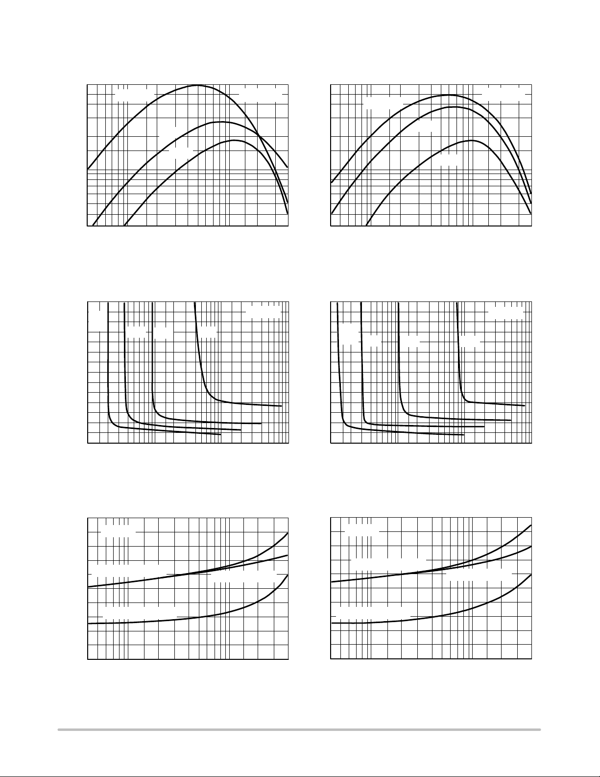
TIP110, TIP111, TIP112 (NPN); TIP115, TIP116, TIP117 (PNP)
6.0 k
4.0 k
3.0 k
2.0 k
1.0 k
, DC CURRENT GAIN
800
FE
h
600
400
300
NPN
TIP110, 111, 112
TJ = 125°C
25°C
-55°C
0.04
0.06 0.1 0.2 0.6 1.0 4.0
IC, COLLECTOR CURRENT (AMP)
3.4
IC =
3.0
0.5 A
2.6
1.0 A
2.0 A
0.4
4.0 A
6.0 k
VCE = 3.0 V
2.0
4.0 k
3.0 k
2.0 k
1.0 k
, DC CURRENT GAIN
800
FE
h
600
400
300
0.04
Figure 8. DC Current Gain
3.4
TJ = 25°C
3.0
2.6
PNP
TIP115, 116, 117
TJ = 125°C
25°C
-55°C
0.06 0.1 0.2 0.6 1.0 4.0
IC, COLLECTOR CURRENT (AMP)
IC =
0.5 A
1.0 A
0.4
2.0 A 4.0 A
VCE = 3.0 V
2.0
TJ = 25°C
, COLLECTOR-EMITTER VOLTAGE (VOLTS)
V
V, VOLTAGE (VOLTS)
CE
2.2
1.8
1.4
1.0
0.6
0.1
0.2 1.0 2.0 20 100
0.5 5.0
IB, BASE CURRENT (mA)
10
Figure 9. Collector Saturation Region
2.2
TJ = 25°C
1.8
V
@ IC/IB = 250
BE(sat)
1.4
1.0
0.6
V
CE(sat)
@ IC/IB = 250
VBE @ VCE = 3.0 V
2.2
1.8
1.4
1.0
, COLLECTOR-EMITTER VOLTAGE (VOLTS)
CE
0.6
50
V
V, VOLTAGE (VOLTS)
0.1
0.2 1.0 2.0 20 100
2.2
1.8
1.4
1.0
0.6
TJ = 25°C
V
CE(sat)
0.5 5.0 50
IB, BASE CURRENT (mA)
V
@ IC/IB = 250
BE(sat)
@ IC/IB = 250
10
VBE @ VCE = 3.0 V
0.2
0.04
0.06 0.1 0.2 0.6 1.0 2.0 4.0
IC, COLLECTOR CURRENT (AMP)
0.4
0.2
0.04 0.06 0.1 0.2 0.6 1.0 2.0 4.0
Figure 10. “On” Voltages
http://onsemi.com
6
0.4
IC, COLLECTOR CURRENT (AMP)

TIP110, TIP111, TIP112 (NPN); TIP115, TIP116, TIP117 (PNP)
NPN
TIP110, 111, 112
, TEMPERATURE COEFFICIENTS (mV/ C)°θ
+0.8
-0.8
-1.6
-2.4
-3.2
-4.0
V
-4.8
*APPLIES FOR IC/IB ≤ hFE/3
0
25°C to 150°C
*qVC for V
CE(sat)
-55°C to 25°C
25°C to 150°C
qVC for V
BE
0.04 0.06 0.2 0.4 0.6 1.0 2.0 4.0
0.1
-55°C to 25°C
IC, COLLECTOR CURRENT (AMP)
Figure 11. Temperature Coefficients
5
10
REVERSE FORWARD
4
10
3
10
10
10
, COLLECTOR CURRENT (A)μI
C
10
10
VCE = 30 V
2
TJ = 150°C
1
0
100°C
25°C
-1
-0.6
-0.4 -0.2 0 +0.2 +0.4 +0.6 +0.8 +1.0 +1.2
VBE, BASE‐EMITTER VOLTAGE (VOLTS)
+1.4
PNP
TIP115, 116, 117
+0.8
*APPLIES FOR IC/IB ≤ hFE/3
0
-0.8
-1.6
*qVC for V
CE(sat)
-2.4
-3.2
qVC for V
-4.0
, TEMPERATURE COEFFICIENTS (mV/ C)°θ
V
-4.8
0.04 0.06 0.2 0.4 0.6 1.0 2.0 4.0
BE
0.1
IC, COLLECTOR CURRENT (AMP)
5
10
REVERSE FORWARD
4
10
3
10
10
10
, COLLECTOR CURRENT (A)μI
C
10
10
VCE = 30 V
2
TJ = 150°C
1
100°C
0
-1
-0.6
25°C
-0.4 -0.2 0 +0.2 +0.4 +0.6 +0.8 +1.0 +1.2
VBE, BASE‐EMITTER VOLTAGE (VOLTS)
25°C to 150°C
-55°C to 25°C
25°C to 150°C
-55°C to 25°C
+1.4
TEST CIRCUIT VOLTAGE AND CURRENT WAVEFORMS
INPUT
MJE254
50 W
50 W
V
= 10 V
BB1
Note A: Input pulse width is increased until ICM = 0.71 A,
NPN test shown; for PNP test
reverse all polarity and use MJE224 driver.
R
BB1
2kW
R
BB2
100 W
+
V
= 0
-
BB2
Figure 12. Collector Cut‐Off Region
VCE MONITOR
100 mH
TUT
+
VCC = 20 V
-
RS =
0.1 W
I
C
MONITOR
INPUT
VOLTAGE
COLLECTOR
CURRENT
COLLECTOR
VOLTAGE
0.71 A
V
CE(sat)
0 V
-5 V
0 V
V
CER
20 V
Figure 13. Inductive Load Switching
http://onsemi.com
7
tw ≈ 3.5 ms (SEE NOTE A)
100 ms

TIP110, TIP111, TIP112 (NPN); TIP115, TIP116, TIP117 (PNP)
l
PACKAGE DIMENSIONS
TO-220
CASE 221A-09
ISSUE AE
NOTES:
1. DIMENSIONING AND TOLERANCING PER ANSI
SEATING
-T-
PLANE
B
4
Q
123
F
T
A
U
C
S
H
K
Z
L
V
R
J
G
D
N
Y14.5M, 1982.
2. CONTROLLING DIMENSION: INCH.
3. DIMENSION Z DEFINES A ZONE WHERE ALL
BODY AND LEAD IRREGULARITIES ARE
ALLOWED.
DIM MIN MAX MIN MAX
A 0.570 0.620 14.48 15.75
B 0.380 0.405 9.66 10.28
C 0.160 0.190 4.07 4.82
D 0.025 0.035 0.64 0.88
F 0.142 0.161 3.61 4.09
G 0.095 0.105 2.42 2.66
H 0.110 0.155 2.80 3.93
J 0.014 0.025 0.36 0.64
K 0.500 0.562 12.70 14.27
L 0.045 0.060 1.15 1.52
N 0.190 0.210 4.83 5.33
Q 0.100 0.120 2.54 3.04
R 0.080 0.110 2.04 2.79
S 0.045 0.055 1.15 1.39
T 0.235 0.255 5.97 6.47
U 0.000 0.050 0.00 1.27
V 0.045 --- 1.15 ---
Z --- 0.080 --- 2.04
MILLIMETERSINCHES
ON Semiconductor and are registered trademarks of Semiconductor Components Industries, LLC (SCILLC). SCILLC reserves the right to make changes without further notice
to any products herein. SCILLC makes no warranty, representation or guarantee regarding the suitability of its products for any particular purpose, nor does SCILLC assume any liability
arising out of the application or use of any product or circuit, and specifically disclaims any and all liability, including without limitation special, consequential or incidental damages.
“Typical” parameters which may be provided in SCILLC data sheets and/or specifications can and do vary in different applications and actual performance may vary over time. All
operating parameters, including “Typicals” must be validated for each customer application by customer's technical experts. SCILLC does not convey any license under its patent rights
nor the rights of others. SCILLC products are not designed, intended, or authorized for use as components in systems intended for surgical implant into the body, or other applications
intended to support or sustain life, or for any other application in which the failure of the SCILLC product could create a situation where personal injury or death may occur. Should
Buyer purchase or use SCILLC products for any such unintended or unauthorized application, Buyer shall indemnify and hold SCILLC and its officers, employees, subsidiaries, affiliates,
and distributors harmless against all claims, costs, damages, and expenses, and reasonable attorney fees arising out of, directly or indirectly, any claim of personal injury or death
associated with such unintended or unauthorized use, even if such claim alleges that SCILLC was negligent regarding the design or manufacture of the part. SCILLC is an Equal
Opportunity/Affirmative Action Employer. This literature is subject to all applicable copyright laws and is not for resale in any manner.
PUBLICATION ORDERING INFORMATION
LITERATURE FULFILLMENT:
Literature Distribution Center for ON Semiconductor
P.O. Box 5163, Denver, Colorado 80217 USA
Phone: 303-675-2175 or 800-344-3860 Toll Free USA/Canada
Fax: 303-675-2176 or 800-344-3867 Toll Free USA/Canada
Email: orderlit@onsemi.com
N. American Technical Support: 800-282-9855 Toll Free
USA/Canada
Europe, Middle East and Africa Technical Support:
Phone: 421 33 790 2910
Japan Customer Focus Center
Phone: 81-3-5773-3850
http://onsemi.com
ON Semiconductor Website: www.onsemi.com
Order Literature: http://www.onsemi.com/orderlit
For additional information, please contact your loca
Sales Representative
TIP110/D
8
 Loading...