

Page 1

Four-Output PTIC Control IC
TCC-404
Introduction
TCC−404 is a four−output high−voltage digital to analog control IC
specifically designed to control and bias ON Semiconductor’s Passive
Tunable Integrated Circuits (PTICs).
These tunable capacitor control circuits are intended for use in
mobile phones and dedicated RF tuning applications. The
implementation of ON Semiconductor’s tunable circuits in mobile
phones enables significant improvement in terms of antenna radiated
performance.
The tunable capacitors are controlled through a bias voltage ranging
from 1 V to 28 V. The TCC−404 high−voltage PTIC control IC has
been specifically designed to cover this need, providing four
independent high−voltage outputs that control up to four different
tunable PTICs in parallel. The device is fully controlled through a
MIPI RFFE digital interface.
Key Features
• Controls ON Semiconductor’s PTIC Tunable Capacitors
• Compliant with Timing Needs of Cellular and Other Wireless System
Requirements
• 30 V Integrated Boost Converter with Four up to 28 V Programmable
DAC Outputs
• Low Power Consumption
• MIPI RFFE Interfaces (1.8 V) with 26 MHz Read and 52 MHz Write
• Automatic On−chip Turbo Calculation − Simplified Turbo Messaging
• ASDIV Switch Support over GPIO Toggle or RFFE Command to
facilitate Dual Settings for two Antennae (Dual Radio)
• Integrated Diode and Reduced External Components
• Reduced Value 2.2 mH − 4.7 mH Inductor
• Small Form Factor 1575 x 1025 mm, WLCSP 4x3 Array
• This is a Pb−Free Device
www.onsemi.com
WLCSP12
CASE 567WF
MARKING DIAGRAM
T44x
ALYWG
G
T44x= Specific Device Code
x = a or b
A = Assembly Location
L = Wafer Lot
Y = Year
W = Work Week
G = Pb−Free Package
(Note: Microdot may be in either location)
ORDERING INFORMATION
See detailed ordering and shipping information on page 39 of
this data sheet.
Typical Applications
• Multi−band, Multi−standard, Advanced and Simple Mobile Phones
• Tunable Antenna Matching Networks
• Compatible with Closed−loop and Open−loop Antenna Tuner
Applications
© Semiconductor Components Industries, LLC, 2019
March, 2021 − Rev. 2
1 Publication Order Number:
TCC−404/D
Page 2

VDDA
GND
L_BOOST VHV
VIO
VDDA
VREG
VHV
Booster
TCC−404
vio_on
ibias_start / vref_start
Regulators
Bandgap
VREG
POR
RC
OSC
VIO
AD
VIO
POR
Start
Reference
Interface
Level
Shifter
CLK DATA
A3
4 bit
DAC
por_vreg
Registers
7 bit
7
DAC
7 bit
7
DAC
7 bit
7
Level
Shifter
OTP
Figure 1. Control IC Functional Block Diagram
A2
A1
A1
OUTD
DAC
7 bit
7
DAC
A2
VHV
OUTA
OUTB
OUTC
OUTD
A3
L_BOOST
B3
C3
B2
C2
B1
C1
D1D2D3
B1
OUTC
C1
OUTB
D1
OUTA
B2
GNDA
C2
AD
D2
DATA
B3
VDDA
C3
VIO
D3
CLK
Figure 2. RDL Padout, Bump Side View (left), PCB footprint (right), with RDL Bump Assignment
www.onsemi.com
2
Page 3
TCC−404
RDL Pin Out
Table 1. PAD DESCRIPTIONS
RDL Name Type Description
A1 OUTD AOH High Voltage Output D
A2 VHV AOH / AIH Boost High Voltage (can be forced externally)
A3 L_BOOST AOH Boost Inductor
B1 OUTC AOH High Voltage Output C
B2 GNDA P Analog Ground
B3 VDDA P Analog Supply
C1 OUTB AOH / AI High Voltage Output B
C2 AD DIO Antenna Diversity (Note 1)
C3 VIO P Digital IO Supply
D1 OUTA AOH / AI High Voltage Output A
D2 DATA DIO MIPI RFFE Digital IO
D3 CLK DI MIPI RFFE Clock
Legend: Pad Types
AIH= High Voltage Analog Input
AOH= High Voltage Analog Output
DI= Digital Input
DIO= Digital Input/Output (IO)
P= Power
1. To be grounded if not utilized.
ELECTRICAL PERFORMANCE SPECIFICATIONS
Table 2. ABSOLUTE MAXIMUM RATINGS
Symbol Parameter Rating Unit
VDDA Analog Supply Voltage −0.3 to +5.5 V
VIO IO Reference Supply Voltage −0.3 to +2.5 V
V
I/O
V
HVH
V
ESD (HBM)
T
STG
T
AMB_OP_MAX
Stresses exceeding those listed in the Maximum Ratings table may damage the device. If any of these limits are exceeded, device functionality
should not be assumed, damage may occur and reliability may be affected.
Input Voltage Logic Lines (DATA, CLK) −0.3 to VIO + 0.3 V
VHV Maximum Voltage −0.3 to 33 V
Human Body Model, JESD22−A114, All I/O 2,000 V
Storage Temperature −55 to +150 °C
Max Operating Ambient Temperature without Damage +110 °C
www.onsemi.com
3
Page 4

TCC−404
Table 3. RECOMMENDED OPERATING CONDITIONS
Rating
Symbol Parameter
T
AMB_OP
T
J_OP
Operating Ambient Temperature −30 − +85 °C
Operating Junction Temperature −30 − +125 °C
VDDA Analog Supply Voltage 2.3 − 5.5 V
VIO IO Reference Supply Voltage 1.62 − 1.98 V
Functional operation above the stresses listed in the Recommended Operating Ranges is not implied. Extended exposure to stresses beyond
the Recommended Operating Ranges limits may affect device reliability.
Min Typ Max
Unit
Table 4. DC CHARACTERISTICS (T
equivalent series load of 5.6 kW and 2.7 nF; C
Symbol
Parameter Min Typ Max Unit Comment
= −30 to +85°C; V
A
= 22 nF; L
HV
= 15 V for each output; 2.3 V<VDDA< 5.5 V; VIO = 1.8 V; R
OUTX
= 2.2 mH; unless otherwise specified)
BOOST
LOAD
=
SHUTDOWN MODE
I
VDDA
I
L_BOOST
I
BATT
I
VIO
I
CLK
I
DATA
VDDA Supply Current − − 1.5 mA
L_BOOST Leakage − − 1.5
Battery Current − − 2.5
VIO Supply Current −1 − 1
CLK Leakage −1 − 1
DATA Leakage −1 − 1
VIO Supply is Low
ACTIVE MODE
I
BATT
Average battery current, 2 outputs actively switching 16 V for 1205 ms to 2 V
− 1200 1600 mA At VHV = 20 V
VDDA = 3.3 V
for 1705 ms to 8 V for 1705 ms
I
BATT_SS0
I
BAT_SS2
I
BATT_SS16
I
L_BOOST
Average battery current, 4 outputs @
0 V steady state
Average battery current, 4 outputs @
2 V steady state
Average battery current, 4 outputs @
16 V steady state
Average inductor current, 2 outputs actively switching 16 V for 1205 ms to 2 V
− 750 950 At VHV = 20 V
VDDA = 3.3 V
− 850 1200 mA At VHV = 20 V
VDDA = 3.3 V
− 1000 1300 At VHV = 20 V
VDDA = 3.3 V
− 1000 1400 At VHV = 20 V
VDDA = 3.3 V
for 1705 ms to 8 V for 1705 ms and 3
outputs are @ 16 V steady state
I
L_BOOST_SS0
I
L_BOOST_SS2
I
L_BOOST_SS16
I
VIO_INACT
I
VIO_ACTIVE
Average inductor current, 4 outputs @
0 V steady state
Average inductor current, 4 outputs @
2 V steady state
Average inductor current, 4 outputs @
16 V steady state
− 550 750 At VHV = 20 V
VDDA = 3.3 V
− 700 1000 At VHV = 20 V
VDDA = 3.3 V
− 850 1100 At VHV = 20 V
VDDA = 3.3 V
VIO average inactive current − − 3 VIO is high, no bus activity
VIO average active current − − 250 VIO = 1.8 V, master sending
data at 26 MHz
LOW POWER MODE
I
VDDA
I
L_BOOST
I
BATT
I
VIO
VDDA Supply Current − − 25 mA
L_BOOST Leakage − − 6
Battery Current − − 31 I
VDDA
+ I
L_BOOST
VIO Supply Current − − 3 No bus activity
Product parametric performance is indicated in the Electrical Characteristics for the listed test conditions, unless otherwise noted. Product
performance may not be indicated by the Electrical Characteristics if operated under different conditions.
www.onsemi.com
4
Page 5

TCC−404
Table 5. BOOST CONVERTER CHARACTERISTICS
(VDDA from 2.3 V to 5.5 V; VIO = 1.8 V; TA = –30 to +85°C; CHV = 22 nF; L
Symbol
VHV_min Minimum programmable output volt-
Parameter Conditions Min Typ Max Unit
Active mode − 15 −
age (average), DAC Boost = 0h
VHV_max Maximum programmable output volt-
Active mode − 30 −
age (average), DAC Boost = Fh
Resolution Boost voltage resolution 4−bit DAC − 1 −
I
L_BOOST_LIMIT
Inductor current limit − 300 − mA
Table 6. ANALOG OUTPUTS (OUT A, OUT B, OUT C, OUT D)
(VDDA from 2.3 V to 5.5 V; VIO = 1.8 V; VHV = 26 V; TA = –30 to +85°C; R
Parameter
SHUTDOWN MODE
Z
OUT
OUT A, OUT B, OUT C, OUT D
output impedance
ACTIVE MODE
V
OH
V
OL
Maximum output voltage − 24 or
Minimum output voltage − − 1 V DAC A, B, C, D = 01h, DAC Boost =
Slew Rate − 3 10
R
PD
OUT A, OUT B, OUT C, OUT D set
in pull−down mode
Resolution Voltage resolution (1−bit) − 189 /
V
OFFSET
Zero scale, least squared best fit −1 − +1 LSB
Gain Error −3.0 − +3.0 %V
DNL Differential non−linearity least
squared best fit
INL Integral non−linearity least squared
best fit
I
SC
V
RIPPLE
Over current protection − 5 65 mA Any DAC output shorted to ground
Output ripple with all outputs at
steady state
Description Min Typ Max Unit Comment
7 − −
28
− − 1000
220
−0.9 − +0.9 LSB 1 V to 24 V with 26 V VHV
−1 − +1 LSB 1 V to 24 V with 26 V VHV
− − 40 mV RMS 1 V to 24 V with 26 V VHV
= 2.2 mH; unless otherwise specified)
BOOST
= ∞ unless otherwise specified)
load
MW
DAC disabled
− V DAC A, B, C, D = 7Fh,
DAC Boost = Fh, I
0h to Fh, I
ms
W
2 V to 20 V step, measured at
V
OUT
R
LOAD
5.6 kW and 2.7 nF, Turbo enabled
DAC A, B, C, D = 00h, DAC Boost =
0h to Fh, selected output(s) is
disabled
− mV (1 LSB = 1−bit) based on VOH
selection
OUT
1 V to 24 V with 26 V VHV
V
< 10 mA
OH
< 10 mA
OH
= 15.2 V,
= equivalent series load of
www.onsemi.com
5
Page 6
TCC−404
THEORY OF OPERATION
Overview
The control IC outputs are directly controlled by
programming the four DACs (DAC A, DAC B, DAC C,
DAC D) through the digital interface.
The DAC stages are driven from a reference voltage,
generating an analog output voltage driving a high−voltage
amplifier supplied from the boost converter (see Figure 1 −
Control IC Functional Block Diagram).
The control IC output voltages can be programmed to
scale from 0 V to 24 V, with 127 steps of 189 mV. The
nominal control IC output can be approximated to 189 mV
x (DAC value).
The control IC output voltages can also be programmed to
scale from 0 V to 28 V, with 127 steps of 220 mV. The
nominal control IC output can be approximated to 220 mV
x (DAC value).
For performance optimization the boost output voltage
(VHV) can be programmed to levels between 15 V and 30 V
via the DAC_boost register (4 bits with 1 V steps). The
startup default level for the boosted voltage is VHV = 28 V.
For proper operation and to avoid saturation of the output
devices and noise issues, it is recommended to operate the
boosted VHV voltage at least 2 V (>4 V [6 V recommended]
if using Turbo−Charge Mode) above the highest
programmed V
Operating Modes
voltage of any of the three outputs.
OUT
The following operating modes are available:
1. Shutdown Mode: All circuit blocks are off, the
DAC outputs are disabled and placed in high Z
state and current consumption is limited to
minimal leakage current. The shutdown mode is
entered upon initial application of VDDA or upon
VIO being placed in the low state. The contents of
the registers are not maintained in shutdown mode.
2. Startup Mode: Startup is only a transitory mode.
Startup mode is entered upon a VIO high state. In
startup mode all registers are reset to their default
states, the digital interface is functional, the boost
converter is activated, outputs OUT A, OUT B,
OUT C and OUT D are disabled and the DAC
outputs are placed in a high Z state. Control
software can request a full hardware and register
reset of the TCC−404 by sending an appropriate
PWR_MODE command to direct the chip from
either the active mode or the low power mode to
the startup mode. From the startup mode the device
automatically proceeds to the active mode.
3. Active Mode: All blocks of the TCC−404 are
activated and the DAC outputs are fully controlled
through the digital interface, DACs remain off
until enabled. The DAC settings can be
dynamically modified and the HV outputs will be
adjusted according to the specified timing
diagrams. Each DAC can be individually
controlled and/or switched off according to
application requirements. Active mode is
automatically entered from the startup mode.
Active mode can also be entered from the low
power mode under control software command.
4. Low Power Mode: In low power mode the serial
interface stays enabled, the DAC outputs are
disabled and are placed in a high Z state and the
boost voltage circuit is disabled. Control software
can request to enter the low power mode from the
active mode by sending an appropriate
PWR_MODE command. The contents of all
registers are maintained in the low power mode.
VDDA = 0
Shutdown
VIO = LOW
automatic
Low Power
(User Defined)
Battery insertion
VIO = HIGH
PWR_MODE =
0bx1
VIO = LOW
PWR_MODE = 0b00
PWR_MODE = 0b10
Figure 3. Modes of Operation
www.onsemi.com
6
Startup
(Registers reset)
PWR_MODE =
0bx1
Active
(User Defined)
Page 7
TCC−404
VDDA Power−On Reset (POR)
Upon application of VDDA, TCC−404 will be in
shutdown mode. All circuit blocks are off and the chip draws
only minimal leakage current.
VIO Power−On Reset and Startup Conditions
A high level on VIO places the chip in startup mode which
provides a POR to TCC−404. POR resets all registers to their
default settings. VIO POR also resets the serial interface
circuitry. POR is not a brown−out detector and VIO needs to
be brought back to a low level to enable the POR to trigger
again.
Table 7. VIO POWER−ON RESET AND STARTUP
Default State for
Register
DAC Boost [1101] VHV = 28 V
Power Mode [01]>[00] Transitions from shutdown to startup and then automatically to active mode
DAC Enable [0000] V
DAC A Output in High−Z Mode
DAC B Output in High−Z Mode
DAC C Output in High−Z Mode
DAC D Output in High−Z Mode
VIO POR
A, B, C, D Disabled
OUT
Comment
VIO Shutdown
A low level at any time on VIO places the chip in shutdown mode in which all circuit blocks are off. The contents of the
registers are not maintained in shutdown mode.
Table 8. VIO THRESHOLDS (VDDA from 2.3 V to 5.5 V; T
Parameter
VIORST VIO Low Threshold − − 0.2 V When VIO is lowered below this threshold level the
Description Min Typ Max Unit Comments
= –30 to +85°C unless otherwise specified)
A
chip is reset and placed into the shutdown mode
Power Supply Sequencing
The VDDA input is typically directly supplied from the battery and thus is the first on. After VDDA is applied and before VIO
is applied to the chip, all circuits are in the shutdown mode and draw minimum leakage currents. Upon application of VIO,
the chip automatically starts up using default settings and is placed in the active state waiting for a command via the serial
interface.
Table 9. TIMING (VDDA from 2.3 V to 5.5 V; V
= 2.2 mH; VHV = 20 V; Turbo−Charge mode off unless otherwise specified)
L
BOOST
Parameter
T
POR_VREG
T
BOOST_START
T
SD_TO_ACT
T
SET+
T
SET−
T
SET+
T
SET−
Internal bias settling time from shutdown to active mode − 50 120
Time to charge CHV @ 95% of set VHV − 130 −
Startup time from shutdown to active mode − 180 250
Timing for a 2 V to 16 V transition, measured when
voltage reaches within 5% of target voltage, measured between the R (5.6 kW) and C (2.7 nF) of an
equivalent PTIC series load.
Timing for a 16 V to 2 V transition, measured when
voltage reaches within 5% of target voltage, measured between the R (5. 6 kW) and C (2.7 nF) of an
equivalent PTIC series load.
Output A, B, C, D positive settling time with Turbo − 35 −
Output A, B, C, D negative settling time with Turbo − 35 −
Description Min Typ Max Unit Comments
= 1.8 V; TA = –30 to +85°C; OUT A, OUT B, OUT C, OUT D; CHV = 47 nF;
IO
For info only
For info only
Voltage settling time
connected on V
Effective PTIC
tuning voltage
settling time,
measured between
an equivalent R and
C PTIC load
Voltage settling time
connected on V
Voltage settling time
connected on V
− 50 60
− 50 60
ms
ms
ms
ms
ms
ms
ms
A, B, C, D
A, B, C, D
A, B, C, D
OUT
OUT
OUT
www.onsemi.com
7
Page 8
TCC−404
g
Figure 4. Output Settling Diagram
Shutdown Startup
VDDA
VIO
vio_on
startup
references
dvreg_en
vreg_short
avreg
dvreg
vref
nvbg_en
vbg_ok
dvreg_on (digital supply monitoring)
nforce_reset = VIO_ON& DVREG_ON)
Active
rc_enable
rc osc
clk_dig = rc_osc 64us after
nforce_reset & vbg_ok & rc_enable
nreset_dig = latched 64us after
(nforce_reset & vbg_ok_osc_on)
OTP read
VHV
32us
T
T
POR_VREG
Fi
boost_start
T
SD_TO_ACT
ure 5. Startup Timing Diagram
www.onsemi.com
8
Page 9
TCC−404
Boost Control
TCC−404 integrates an asynchronous current control
boost converter. It operates in a discontinuous mode and
features spread−spectrum circuitry for Electro−Magnetic
Interference (EMI) reduction.
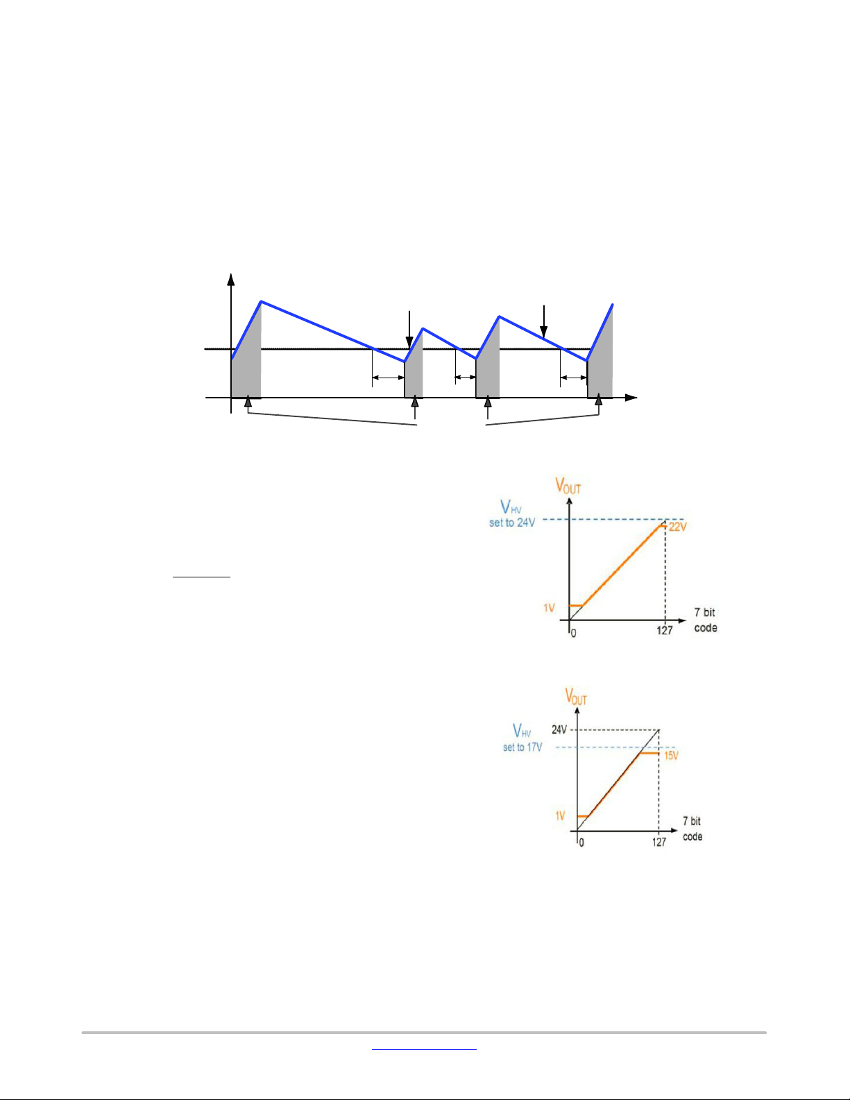
Boost Output Voltage (VHV) Control Principle
The asynchronous control starts the boost converter as
soon as the VHV voltage drops below the reference set by
the 4−bit DAC and stops the boost converter when the VHV
voltage rises above the reference again.
Recharge
Set
VHV
Figure 6. VHV Voltage Waveform
High Impedance (High Z) Feature
In shutdown mode the OUT pins are set to a high
impedance mode (high Z). Following is the principle of
operation for the control IC:
1. The DAC output voltage V
OUT
DAC code
+
127
24 or 28 V
V
is defined by:
OUT
(eq. 1)
2. The RFFE_REG_0x05 controls the range of the
DAC (24 or 28 V).
3. The voltage VHV defines the maximum supply
voltage of the DAC supply output regulator and is
set by a 4−bit control.
4. The maximum DAC DC output voltage V
OUT
is
limited to (VHV – 2 V). DAC can achieve higher
output voltages, but timing is not maintained for
swings above VHV − 2 V.
5. The minimum output DAC voltage V
OUT
is 1.0 V
max.
CHV
Delay
Due to the slow response time of the control loop, the
VHV voltage may drop below the set voltage before the
control loop compensates for it. In the same manner, VHV
can rise higher than the set value. This effect may reduce the
maximum output voltage available. Please refer to Figure 6
below.
The asynchronous control reduces switching losses and
improves the output (VHV) regulation of the DC/DC
converter under light load, particularly in the situation
where TCC−404 only maintains the output voltages to fixed
values.
CHV
Boost
Running
Discharge
Delay
Figure 7. DAC Output Range Example A
VHV
Delay
Time
www.onsemi.com
9
Figure 8. DAC Output Range Example B
Page 10

TCC−404
Digital Interface
The control IC is fully controlled through a digital
interface (DATA, CLK). The digital interface is described in
the following sections of this document.
Turbo−Charge Mode
The TCC−404 control IC has an autonomous
Turbo−Charge Mode that significantly shortens the system
settling time when changing programming voltages.
In Turbo−Charge Mode the DAC output target voltage is
temporarily set to either a delta voltage above or a delta
voltage below the actual desired target. The delta voltage is
4 volts.
After the DAC value message is received, the delta
voltage is calculated by hardware, and is applied in digital
format to the input of the DAC, right after trigger is received.
The period for which the delta voltage is maintained to the
input of the DAC, the Turbo time, is autonomously
calculated and based on the following considerations:
• DACA CONTROL[1:0] / DACB CONTROL[1:0] /
DACC CONTROL[1:0] / DACD CONTROL[1:0] :
These are the DAC operational mode control bits. The
bit[0] in the control defines the step size of the DAC as
189 mV (0) or 220 mV (1). The bit[1] in the control
enables the autonomous turbo mode. In order the Turbo
operation to be enabled each DAC has to have this bit
set. Otherwise the DAC values are applied without
Turbo.
• TurboUpMultiplier[2:0]: If the Turbo direction is UP,
the base autonomous Turbo time calculated is
multiplied with this configuration factor. The default
state of this configuration provides the optimum time
for the Turbo UP operation. The factor decoding is as
below:
‘000’: multiplication by 1.0
‘001’: multiplication by 1.125
‘010’: multiplication by 1.25
‘011’: multiplication by 1.375 (default)
‘100’: multiplication by 1.5
‘101’: multiplication by 1.625
‘110’: multiplication by 1.75
‘111’: multiplication by 1.875
• TurboDownMultiplier[2:0]: If the Turbo direction is
DOWN, the base autonomous Turbo time calculated is
multiplied with this configuration factor. The default
state of this configuration provides the optimum time
for the Turbo DOWN operation. The factor decoding is
as below:
‘000’: multiplication by 1.0
‘001’: multiplication by 1.125
‘010’: multiplication by 1.25
‘011’: multiplication by 1.375 (default)
‘100’: multiplication by 1.5
‘101’: multiplication by 1.625
‘110’: multiplication by 1.75
‘111’: multiplication by 1.875
• TurboDownFactor[1:0]: If the Turbo direction is
DOWN and the target voltage is below 4V the Turbo
time calculation further adjusted with this factor. The
default setting provides the optimum Turbo DOWN
operation.
• GL_A / GL_B / GL_C / GL_D: These are the DAC
update mode configuration fields, which need to be set
to turbo mode at the new DAC value update and prior
to the SW trigger (optional). These bits are part of the
DAC value register. If they are set to 0, the DAC is in
Turbo Mode, as long as the corresponding DAC
CONTROL register is configured so. If the Turbo is not
enabled the DAC value is applied as is.
• The Turbo UP or DOWN voltage is decided based on
the comparison of the new DAC value and the old DAC
value. If the new value is greater, the turbo direction
will be UP. Otherwise it will be DOWN. In case of both
DAC values being equal, there is no DAC update
applied. After a turbo request is received, any trigger
will start the turbo output transition. The trigger could
be:
♦ A MIPI−RFFE software trigger controlled by
RFFE_PM_TRIG register
♦ An AD pad toggle if the GPIO is enabled as trigger
source or MIPI−RFFE command is sent to trigger
the AD.
♦ An internal generated trigger after the corresponding
DAC value is updated, as described in section DAC
Update Triggering.
The DAC values send by digital turbo−charge logic to
DACs are:
• During turbo−charge delay duration the value applied is
“DAC_new ±4 V” (the polarity of the 4 V turbo will
depend on if turbo charge is up or down)
• If DAC_new > DAC old, and DAC_new+4 V is
exceeding the word length of the DAC, it is saturated to
max value possible.
• If DAC_new < DAC_old, and DAC_new−4 V is a
negative number, a DAC value of 0 is applied.
♦ After turbo−charge delay duration the value applied
is the actual DAC_new.
www.onsemi.com
10
Page 11

TCC−404
Table 10. GLIDE TIMER STEP DURATION
DAC GLIDE TIMER [4:0]
Bit 4 Bit 3 Bit 2 Bit 1 Bit 0
0 0 0 0 0 2
0 0 0 0 1 4
0 0 0 1 0 6
0 0 0 1 1 8
0 0 1 0 0 10
0 0 1 0 1 12
0 0 1 1 0 14
0 0 1 1 1 16
0 1 0 0 0 18
0 1 0 0 1 20
0 1 0 1 0 22
0 1 0 1 1 24
0 1 1 0 0 26
0 1 1 0 1 28
0 1 1 1 0 30
0 1 1 1 1 32
1 0 0 0 0 34
1 0 0 0 1 36
1 0 0 1 0 38
1 0 0 1 1 40
1 0 1 0 0 42
1 0 1 0 1 44
1 0 1 1 0 46
1 0 1 1 1 48
1 1 0 0 0 50
1 1 0 0 1 52
1 1 0 1 0 54
1 1 0 1 1 56
1 1 1 0 0 58
1 1 1 0 1 60
1 1 1 1 0 62
1 1 1 1 1 64
Glide Step Duration in Glide Mode [ms]
Transition from Turbo to Turbo or Immediate Update
In the event a new trigger is received during a turbo
transition, the ongoing turbo operation is halted and the new
DAC value is applied immediately. There won’t be any
Turbo and the hi_slew is kept low.
Transition from Turbo to Glide
In the event that a new glide transition is triggered during
a turbo event, then the turbo process is stopped and the
current target value is set at the DAC output immediately
without hi_slew. The new glide is started from this value.
www.onsemi.com
DAC Disable during Turbo (including active to low
power mode transition)
If the DAC, which is in Turbo is disabled, the target DAC
value is immediately applied without hi_slew. The DAC
does not continue with the Turbo when it is re−enabled.
Turbo coming out of Low Power Mode
If the DAC, which is in low power mode is triggered with
a new Turbo DAC update, the DAC_old value is taken as 0V
in autonomous Turbo calculation.
11
Page 12

TCC−404
Glide Mode
The TCC−404 control IC has a Glide Mode that
significantly extends the system transition time when
changing programming voltages.
Glide Mode is controlled by the following registers:
• GLIDE TIMER STEP SIZE [4:0]: This register is used
only in glide mode and shared between all DACs. It
defines the step duration of each glide step. If each
DAC is updated over and over with the same glide step,
these fields do NOT need to be updated at each DAC
update. The various configuration values are listed in
Table 10.
• GL_A / GL_B / GL_C / GL_D: These are the DAC
updatemode configuration fields, which need to be set
to glide mode at the new DAC value update and prior to
the SW trigger (optional). These bits are part of the
DAC value register. If they are set to 1, the DAC is in
glide mode.
After a Glide request is received, any trigger will start the
Glide output transition.
The trigger could be:
• a MIPI−RFFE software trigger controlled by
RFFE_PM_TRIG register
• An AD pad toggle if the GPIO is enabled as trigger
source or MIPI−RFFE command is sent to trigger the
AD
• an internal generated trigger after the corresponding
DAC value is updated, as described in a later section.
Immediately after the trigger, the DAC_old value is loaded
in the MSB’s of the upper byte of a 15 bit accumulator, while
the lower byte of accumulator is being reset to 0x00.
At the same time a count step is calculated:
GLIDE_STEP[6:0] = DAC_new – DAC_old; if
DAC_new > DAC_old
GLIDE_STEP[6:0] = DAC_old – DAC_new; if
DAC_new < DAC_old
ACCUMULATOR[14:0] = DAC_old, 0x00;
NOTE: Glide is disabled if DAC_new = DAC_old.
From the moment the trigger is received, a tick is
generated internally, with a frequency controlled by the
GLIDE TIMER STEP SIZE register. Each DAC has its own
tick generator running independently of the other DAC.
Each time a trigger is received for a DAC, the setting of the
GLIDE TIMER STEP SIZE register is sampled in a counter
dedicated to that DAC. Any update of the GLIDE TIMER
STEP SIZE register after trigger is received will be ignored
until the next trigger is received
Each time a tick is generated, the content of the
accumulator is either incremented or decremented,
depending whether DAC_new is either bigger or smaller
than DAC_old.
ACCUMULATOR[14:0] = ACCUMULATOR[14:0] +
GLIDE_STEP; if DAC_new > DAC_old
ACCUMULATOR[14:0] = ACCUMULATOR[14:0] −
GLIDE_STEP; if DAC_new < DAC_old
Each time a tick is generated, the output of the DAC[6:0]
is updated with the value of ACCUMULATOR[14:8];
The Gliding process continues until, upper 7 bits of the
accumulator matches the value of the DAC_new.
ACCUMULATOR[14:8] ≥ DAC_new, when DAC_new
> DAC_old
ACCUMULATOR[14:8] ≤ DAC_new, when DAC_new
< DAC_old
The Glide timer will reference the 2 MHz clock divided to
provide between 2 ms and 64 ms per glide step.
Each DAC is independent in terms of its switching
operation, thus each DAC may be independently
programmed for Normal, Turbo or Glide regardless of the
switching operation of the other DACs.
Transition from Glide to Glide
In the event a new glide request is received during a glide
transition, the ongoing glide operation is halted and the new
glide operation is started from the DAC value, where the
previous glide has left off. The DAC timers can be updated
to a new value at the trigger.
Transition from Glide to Turbo or Normal Switching
In the event that a new Normal switching or Turbo DAC
value is received during a Glide transition, then the Glide
process is stopped and the DAC immediately switches to the
newly received target value without Turbo or Glide. The
hi_slew is not applied.
DAC Disable during Glide (including active to low
power mode transition)
If the DAC, which is gliding is disabled, the DAC value
holds on to the value where the glide stops. The DAC does
not continue with the glide when it is re−enabled. It drives
the last calculated DAC value without a hi_slew.
www.onsemi.com
12
Page 13

TCC−404
ASDIV − Dual Radio Control
The TCC−404 carries two sets of registers (Radio0 and
Radio1) for only DAC_A/B/C/D Value Registers. The
Radio0 set consists of RFFE_REG_0x06,
RFFE_REG_0x07, RFFE_REG_0x08, RFFE_REG_0x09.
The Radio1 set consists of RFFE_REG_0x0A,
RFFE_REG_0x0B, RFFE_REG_0x0C,
RFFE_REG_0x0D. These registers set the actual DAC
values when their set is active and control the glide turn on
and off.
The Dual Radio Control field at RFFE_REG_0x0E
register governs the operation of the Dual Radio
functionality. The AD pad can be enabled to switch between
the Radio0 and Radio1 values according to the state of this
pad. The reset state of this register is to disable the Dual
Radio operation.
The control register has the following states:
0: The AD (Antenna Diversity) pad is disabled. There is
no toggling between the Radio0 and Radio1 Registers. The
Radio0 DAC registers are used as the active shadow
registers for trigger.
1: The AD (Antenna Diversity) pad is enabled. The
Radio0 register set is triggered when the pad input
transitions into “0” from “1”. The Radio1 register set is
triggered when the pad input transitions into “1” from “0”.
The RC clock domain retimed AD pad value defines which
set of shadow registers are active for all triggering purposes.
2: The AD (Antenna Diversity) pad is disabled. The
Radio0 DAC registers are triggered in any transition into
this control value. Rewriting of the same value does not issue
a re−trigger. The RC clock domain retimed register activates
the Radio0 set of registers. A SW trigger or immediate
update captures these Radio0 shadow content into active
registers in any consecutive triggering.
3: The AD (Antenna Diversity) pad is disabled. The
Radio1 DAC registers are triggered in any transition into
this control value. . Rewriting of the same value does not
issue a re−trigger. The RC clock domain retimed register
activates the Radio1 set of registers. A SW trigger or
immediate update captures these Radio1 shadow content
into active registers in any consecutive triggering.
The AD pad does not have any pull on it. It has to be
physically connected to ground or VIO supply
externally. The RC domain retimed state of the dual radio
control can be observed through the upper nibble of the Dual
radio control register (0x0E). A write into this field is
ignored. The sampling of the AD pad is blocked during any
RFFE communication to prevent trigger collision between
the AD pad and the RFFE Interface. Since the conventional
triggering occurs at the end of an RFFE frame, this aligns all
sources of triggering.
If a DAC is disabled, the dual radio triggering does not
apply to this DAC. It holds the last triggered active register
value prior to getting disabled.
ASDIV − Dual Radio Operation Disabled (State0)
This is the single Radio operation, where the Radi0 set of
registers in address range 0x06 to 0x09 are the shadow
registers mapped to active registers. They are triggered by
either immediate update (depending on SW trigger
masking) or SW trigger.
The AD pad state is still captured at RC oscillator clock
domain continuously. This register output can still be read
over the RFFE interface at the dual radio control address
(0x0E). This reading does not reflect the active DAC
register. The active DAC register is enforced to be the
Radio0 set.
This allows the AD pad to be utilized for any system signal
state detection when the dual radio is not active.
In this mode of operation the data read back from the
Radio0 or Radio1 set of registers always returns the
triggered active data sourced from Radio0 set of registers
ASDIV – AD PAD Enabled (State1)
The AD pad defines the active set of registers for
triggering. At each transition of the AD pad the
corresponding set of DAC value registers are triggered.
Only the set of registers the AD pad is pointing to can be
used to trigger an immediate update. In case of the SW
trigger enable, only the registers AD pad is activating will be
triggered. Therefore there is no possibility to trigger Radio0
and Radio1 set of registers at the same time.
The read back from Radio0 or Radio1 set of registers
return only the triggered active register values. The source
of the trigger could be either set, only the current active
register is read back.
If any exit from this mode is requested, the active registers
hold their state (unless the request is to transition into State2
or State3). The exit itself is not a source of trigger.
If the AD Pad value switches under low power mode, the
state of the pad can’t be detected until the part is active and
the DACs are re−enabled. At this point, if its state is different
than the state entering into low power mode, the trigger is
applied.
ASDIV – Dual Radio over RFFE – Radio0 Trigger
(State2)
The AD pad value is ignored in this mode of operation.
The status register at address 0x0E reflects the current active
set of Radio registers. In case of the low power mode, there
could be a difference between this reading and the dual radio
control register value, since the register would not be
sampled until the part goes back to active mode.
The transition into this state triggers the Radio0 set of
registers. If the register is updated as part of an extended
register write, the trigger waits until the end of the frame.
This way under the same frame the corresponding Radio0
registers can be updated and a trigger is requested.
The immediate update or SW triggering can still be
utilized using the Radio0 set of registers.
www.onsemi.com
13
Page 14

TCC−404
The read back from the Radio0 or Radio1 addresses return
the active register values triggered from the Radio0 source.
While in this mode the Radio1 registers can still be
updated. This will not trigger anything.
The exit from this state itself is not a source of trigger.
If the transition into this state occurs during the low power
mode, the trigger is applied as soon as the part is out of the
low power mode and the DACs are re−enabled.
This Dual Radio triggering over the RFFE Interface has
to respect the same timing as the SW triggering
ASDIV – Dual Radio over RFFE – Radio1 Trigger
(State3)
The AD pad value is ignored in this mode of operation.
The status register at address 0x0E reflects the current active
set of Radio registers. In case of the low power mode, there
could be a difference between this reading and the dual radio
control register value, since the register would not be
sampled until the part goes back to active mode.
The transition into this state triggers the Radio1 set of
registers. If the register is updated as part of an extended
register write, the trigger waits until the end of the frame.
This way under the same frame the corresponding Radio1
registers can be updated and a trigger is requested.
The immediate update or SW triggering can still be
utilized using the Radio1 set of registers.
The read back from the Radio0 or Radio1 addresses return
the active register values triggered from the Radio1 source.
While in this mode the Radio0 registers can still be
updated. This will not trigger anything.
The exit from this state itself is not a source of trigger.
If the transition into this state occurs during the low power
mode, the trigger is applied as soon as the part is out of the
low power mode and the internal oscillator has started.
The Dual Radio triggering over the RFFE Interface has to
respect the same timing as the SW triggering.
ASDIV – Glide Handling
The glide operation under the dual radio triggering can be
governed globally for all DACs using the Glide Control field
of the RFFE_REG_0x0E. The intension is to help reducing
the RFFE transactions necessary. In its default state of
State0, the glide is purely controlled by the GL_X fields of
the DAC value registers.
When the glide control is set to State1, after each dual
radio triggering, the corresponding GL bit of the DAC target
rffe register is cleared. This allows a “single shot” operation,
where the GL_X bits in DAC target registers are considered
as a single execution order.
If the dual radio triggering should not be resulting in any
glide at all, the glide control can be set to State2. This is
effectively a global mask to GL bits in dual radio triggering.
The DAC rffe registers hold on to their GL values, the dual
radio triggering ignores them.
If the dual radio triggering should always execute a glide
in transitions, the glide control can be set to State3. In this
case again the GL bits in the source rffe registers hold on to
their values. The dual radio triggering enforces the glide bits
to be set during the triggering.
www.onsemi.com
14
Page 15

TCC−404
DAC Update Triggering
The entire digital logic responsible for DAC updates is
using the clock provided by the internal RC oscillator. In
order to minimize the power consumption, the RC clock is
set at a low frequency around 2 MHz.
DAC Writes
Figure 9 shows the diagram of the DAC data path, from
the moment data is written into DACx_value register, until
it is sent out to DAC.
After the DACx_value register is written using
MIPI−RFFE clock, the data is copied on RC clock domain,
into the first data stage represented in Figure 9 as
‘Completed’. The data is moved into ‘New’ and ‘DAC−Out’
stages by the DAC driver state machine, once the trigger is
detected. The Turbo path also highlights the glide
calculation.
If SW trigger is not enabled, then data will flow through
the stages right after the corresponding DAC is updated,
without waiting for a trigger (MIPI write is considered as the
trigger).
Figure 9. DACx Data Path
To bypass the SW trigger and enable an immediate trigger
the Mask bits under the RFFE_PM_TRIG register should be
set according to the USID control of the DAC. Trigger Mask
2 is controller with USID_2, Trigger Mask 1 is controlled
with USID_1 and Trigger Mask 0 is controlled with USID_0.
In MIPI−RFFE configuration, if RFFE_PM_TRIG /
Trigger_Mask_2 = ‘1’, and RFFE_PM_TRIG /
Trigger_Mask_1 = ‘1’ and RFFE_PM_TRIG /
Trigger_Mask_0 = ‘1’ (all software triggers are masked), then
each DAC value is copied into ‘Completed’ stages of each
DAC, after the messages RFFE_REG_0x06,
RFFE_REG_0x07, RFFE_REG_0x08 or
RFFE_REG_0x09 respectively are received, as shown in
following sequence.
MIPI_RFFE_WRITE #1: send DAC_A_value and
glide/turbo mode to RFFE_REG_0x06
MIPI_RFFE_WRITE #2: send DAC_B_value and
glide/turbo mode to RFFE_REG_0x07
MIPI_RFFE_WRITE #3: send DAC_C_value and
glide/turbo mode to RFFE_REG_0x08
MIPI_RFFE_WRITE #4: send DAC_D_value and
glide/turbo mode to RFFE_REG_0x09
The individual writes above could be combined into a
single extended write with all DACs controlled with the
same USID or the DURs of the DACs are sitting at “11”
configuration. Right after MIPI_RFEE_WRITE #1 to
RFFE_REG_0x06, above, is received the DAC_A value
register is copied in ‘Completed’ stage of DAC_A. The glide
step, dac control or turbo control DO NOT need to be
updated for each DAC update. But if they need to be, they
can be updated as part of a full extended write or single write
prior to the DAC value updates without any timing
limitation. Since the SW trigger is masked, next RC clock
cycle after DAC values are copied in ‘Completed’ stage, the
data will move in next stages ‘New’ and ‘DAC−Out’
without waiting for any trigger.
The similar events occur for DAC_B, DAC_C and
DAC_D after the MIPI_RFEE_WRITE #2 and
MIPI_RFEE_WRITE #3.
Due to the fact that the MIPI−RFFE master can send
DAC updates messages at a higher frequency, than RC
clock, the data buffer ‘Completed’, can be overwritten if
new DAC updates occur in
the same time when the buffer is
loaded.
www.onsemi.com
15
Page 16

TCC−404
While data and configuration are copied from
DACx_value register into ‘Completed’ stage, the
MIPI−RFFE master must not send any new DAC updates to
DACx_value registers or configurations. The time required
for the data to be copied from DACx_value register into
‘Completed’ stage is Max 1500 ns, which is defined by the
three RC clock cycles required to synchronize data from
MIPI−RFFE clock domain to RC clock domain.
In Figure 10, DAC_UPDATE_LAT represents the period
when MIPI−RFFE master is not allowed to send any new
DAC updates to DACx_value registers and DAC
configuration registers.
DAC_UPDATE_LAT = Min 1500ns
A) RADIO0 DAC updates without SW_TRIG
AD PAD enabled at State0
RFFE_REG_0x03to RFFE_REG_0x05 RFFE_REG_0x06/7/8/9 RFFE_REG_0x03 to RFFE_REG_0x09
B) RADIO0 DAC updates with SW_TRIG
AD PAD enabled at State0
RFFE_REG_0x03to RFFE_REG_0x09
The DAC enables (RFFE_REG_0x00) and Booster
configurations (RFFE_REG_0x02) are applied
immediately without waiting any trigger. These registers
should be configured prior, so that the DAC updates are
effective as fast as possible.
If there is already an ongoing DAC update and the Dual
Radio control is changed, this is considered as a transition.
Even if the dual radio triggering occurs in lesser than
DAC_UPDATE_LAT duration from the RFFE triggering,
this is handled as a proper transition.
It takes approximately the same duration as an RFFE
trigger to propagate the dual radio trigger
TRIG Edge
RFFE_REG_0x03to RFFE_REG_0x09
DAC_UPDATE_LAT = Min 1500ns
A) RADIO1 DAC updates without SW_TRIG
AD PAD enabled at State1
RFFE_REG_0x03to RFFE_REG_0x5 RFFE_REG_0x0A/B/C/D
B) RADIO1 DAC updates with SW_TRIG
AD PAD enabled at State1
RFFE_REG_0x03 to RFFE_REG_0x05 and
RFFE_REG_0x0A to RFFE_REG_0x0D
Figure 10. DAC_UPDATE_LAT Requirement
The SW trigger as well as immediate trigger can be
configured in many combinations using the DUR settings of
the DACs and the USID values. The SW trigger masks can
only be changed with the write access using the slave
address of their corresponding USID. But the corresponding
triggers can be set by accesses over broadcast, with
broadcast ID (0x0) or GSID.
The triggering and DAC register access is governed by
these rules:
• The DUR configuration assigns a DAC to a USID. The
corresponding DAC registers can only be accessed with
USID defined by its DUR.
DAC_UPDATE_LAT = Min 1500ns
RFFE_REG_0x03 to RFFE_REG_0x05 and
RFFE_REG_0x0A to RFFE_REG_0x0D
TRIG Edge
RFFE_REG_0x03to RFFE_REG_0x05 and
RFFE_REG_0x0A to RFFE_REG_0x0D
DAC_UPDATE_LAT = Min 1500ns
• The immediate update of this DAC is enabled if the SW
trigger mask of the corresponding USID is set (disabled).
• The PM_TRIG register bit0 (SW trigger0) is masked by
bit4 and assigned to DACs triggering, which are mapped
to USID0 or all USIDs (the DAC DUR=0 or 3).
• The PM_TRIG register bit1 (SW trigger1) is masked by
bit5 and assigned to DACs triggering, which are mapped
to USID1 or all USIDs (the DAC DUR=1 or 3).
• The PM_TRIG register bit2 (SW trigger2) is masked by
bit6 and assigned to DACs triggering, which are mapped
to USID2 or all USIDs (the DAC DUR=2 or 3).
www.onsemi.com
16
Page 17

TCC−404
• For a DAC with DUR=3, all SW masks need to be set
for that DAC to be triggered with direct access to its
target register.
If all DACs are kept at DUR values of 3 and the USIDs are
kept the same (reset condition), the part behaves according
to the MIPI spec with single USID. If some of the USIDs are
different while DUR=3, the part responds to the accesses
with these different USIDs the same fashion.
If all USIDs are kept equal, the part functions with a single
USID. But the DUR settings still control the SW trigger
mapping for the DACs independent of the USID values. The
DACs which are not holding a DUR value of 3 will be under
the control of the SW trigger−mask duo mapped by their
DUR setting.
In Table 11 some example register settings for listed
functionality are provided. For the given functionality the
response of the part to DAC updates and SW triggers are
tabulated. In this table the “DAC trigger” corresponds to a
trigger happening at the time of the DAC value update. The
“SW trigger” corresponds to a trigger happening with the
PM_TRIG register write. At this point, it is assumed that the
DACs are enabled and the new DAC value is not matching
to the existing pre−triggered DAC value in the active
register. Some of the abbreviations utilized in the table are:
TRG = successful trigger of the new targets
HLD = no trigger, hold on to existing DAC drives
WR = The new DAC values are captured into RFFE shadow
registers
NW = The RFFE write to shadow registers are blocked, no
register update.
www.onsemi.com
17
Page 18

TCC−404
Table 11. IMMEDIATE vs SOFTWARE TRIGGERING USING USIDs and DURs
DACA
DACA
DACA
DACA
Trigger
Trigger
Trigger
Trigger
FUNCTIONALITY & EXAM-
PLE REGISTER VALUES
(DEFAULT) DAC TRIGGER
– SINGLE USID – DUR=3
DUR_A = 3 (USIDx, TRGx)
SW−TRG Mask = 3’b111
USID0,1,2 = 4b0111
SW TRIGGER −SINGLE
USID – DUR =3
DUR_A = 3 (USIDx, TRGx)
SW−TRG Mask = 3’b101
USID0,1,2 = 4b0111
DAC TRIGGER −SINGLE
USID – DUR=0
DUR_A = 0 (USID0, TRG0)
SW−TRG Mask = 3’b101
USID0,1,2 = 4b0111
SW TRIGGER −SINGLE
USID – DUR =1
DUR_A = 1 (USID1, TRG1)
SW−TRG Mask = 3’b101
USID0,1,2 = 4b0111
DAC TRIGGER – (1,2)
USIDs – DUR=2
DUR_A = 2 (USID2, TRG2)
SW−TRG Mask = 3’b100
USID0,1 = 4b0111, USID2 =
4b1000
SW TRIGGER – (1,2)
USIDs – DUR =2
DUR_A = 2 (USID2, TRG2)
SW−TRG Mask = 3’b000
USID0,1 = 4b0111, USID2 =
4b1000
DAC TRIGGER – (2,1)
USIDs – DUR = 1
DUR_A = 1 (USID1, TRG1)
SW−TRG Mask = 3’b110
USID0,1 = 4b0111, USID2 =
4b1000
SW TRIGGER – (2,1)
USIDs –DUR = 1
DUR_A = 1 (USID1, TRG1)
SW−TRG Mask = 3’b100
USID0,1 = 4b0111, USID2 =
4b1000
DAC TRIGGER – (1,1,1)
USIDs – DUR = 0
DUR_A = 0 (USID0, TRG0)
SW−TRG Mask = 3’b001
USID0 = 4b0111, USID1 =
4b1000, USID2 = 4b1001
SW TRIGGER – (1,1,1)
USIDs – DUR = 0
DUR_A = 0 (USID0, TRG0)
SW−TRG Mask = 3’b000
USID0 = 4b0111, USID1 =
4b1000, USID2 = 4b1001
WR
ID0
TRG
(WR)
HLD
(WR)
TRG
(WR)
HLD
(WR)
HLD
(NW)
HLD
(NW)
TRG
(WR)
HLD
(WR)
TRG
(WR)
HLD
(WR)
WR
ID1
TRG
(WR)
HLD
(WR)
TRG
(WR)
HLD
(WR)
HLD
(NW)
HLD
(NW)
TRG
(WR)
HLD
(WR)
HLD
(NW)
HLD
(NW)
WR
ID2
TRG
(WR)
HLD
(WR)
TRG
(WR)
HLD
(WR)
TRG
(WR)
HLD
(WR)
HLD
(NW)
HLD
(NW)
HLD
(NW)
HLD
(NW)
WR
3b111
3b111
Broad
ID0
HLD
HLD HLD HLD HLD HLD HLD HLD All USIDs are the same. All
ID1
3b111
ID2
(NW)
HLD
TRG TRG TRG TRG HLD TRG HLD All USIDs are the same.
(NW)
HLD
HLD HLD HLD HLD HLD HLD HLD All USIDs are the same.
(NW)
HLD
TRG TRG TRG TRG HLD TRG HLD All USID’s are the same.
(NW)
HLD
HLD HLD HLD HLD HLD HLD HLD USID2 is different, only
(NW)
HLD
HLD HLD TRG TRG HLD HLD TRG USID2 is different, only
(NW)
HLD
HLD HLD HLD HLD HLD HLD HLD Since USID0 = USID1 both
(NW)
HLD
TRG TRG HLD TRG HLD TRG HLD Same as above but SW
(NW)
HLD
HLD HLD HLD HLD HLD HLD HLD The DAC is mapped to
(NW)
HLD
TRG HLD HLD TRG TRG HLD HLD The DAC is mapped to
(NW)
3b111
Broad
Trigger
3b001
Broad
Trigger
3b010
Broad
Trigger
3b100
Broad
Comments
SW triggers are masked.
The USID DAC writes trigger immediately.
Only trigger 1 is enabled.
This enables the SW trigger since DUR=3, mapping
the DAC to all triggers
Only trigger 1 is enabled.
The DUR of the DAC is
mapping it to trigger 0
(masked). Therefore SW
trigger is disabled.
Only trigger 1 is enabled.
The DUR of the DAC is
mapping it to trigger 1 (enabled). Therefore SW trigger is enabled.
USID2 dac access is allowed and the DAC triggers immediately, since the
SW trigger mask is set.
USID2 dac access is allowed. Trigger 2 is unmasked, SW trigger is enabled. Only trigger 2 is active for USID2.
USID0, USID1 DAC target
writes are allowed. SW
trigger1 masked; SW triggering disabled
trigger 1 is enabled; SW
triggering enabled. USID0,
USID1 are the same but
the DAC is mapped to Trg1
only. Trg0 alone does not
trigger.
USID0 and the corresponding trigger is
masked. It triggers immediately at DAC update with
USID0
USID0 and the TRG0 is
enabled. It triggers only at
TRG0 with USID0 or
Broadcast access
www.onsemi.com
18
Page 19

TCC−404
MIPI RFFE Interface
TCC−404 is a slave device and is compliant to the MIPI
Alliance Specification for RF Front−End Control Interface
(RFFE) Version 2.0 excluding the interrupt support,
extended long R/W, double byte product ID and dual GSID.
Following MIPI RFFE commands are supported:
1. Register 0 WRITE
2. Register WRITE
3. Register READ
4. Extended Register WRITE
5. Extended Register READ
Registers 0x00 to 0x3F are available to be read/written.
The writes in extended speed frequency and reads in
standard speed frequency are supported. The slew rate on the
read access can be configured by the SDATA Pad Slew bit.
The extended register write long and read long commands
are not supported. If an extended register write long
command is received, no register is written and the
RFFE_STATUS.WURE flag is set. If an extended register
read long command is received, the part responds with bus
idle and the RFFE_STATUS.RURE flag is set.
The read access to registers RFFE_REG_0x03 to
RFFE_REG_0x0D returns the active register content,
which is the register updated after a trigger. The pre−trigger
shadow register does not have read access.
Some registers are exact remapping to meet the RFFE 2.0
register mapping. The GSID is mapped to both address 0x1B
and 0x22. The UDR_RST is mapped to both address 0x1A
and 0x23. The ERR_SUM is mapped to both address 0x24
and 0x1A.
This can reduce EMI in expense of longer read delay.
Table 12. MIPI RFFE INTERFACE SPECIFICATION
= −30 to +85°C; 2.3 V < VDDA < 5.5 V; 1.1 V < VIO < 1.8 V; unless otherwise specified)
(T
A
Parameter
F
SCLK_EXT
T
SCLK_EXT
T
SCLKIH_EXT
T
SCLKIL_EXT
F
SCLK_STD
T
SCLK_STD
T
SCLKIH_STD
T
SCLKIL_STD
V
TP
V
TN
V
H
I
IH
I
IL
C
CLK
C
DATA
TD
SETUP
TD
HOLD
T
READ_ACCESS
T
READ_ACCESS
Clock Extended Speed
Frequency
Clock Extended Speed Period 0.0192 − 32
CLK Input Extended High Time 6.0 − − ns Extended Speed
CLK Input Extended Low Time 6.0 − − ns Extended Speed
Clock Standard Speed Frequency
Clock Standard Speed Period 0.038 − 32
CLK Input Standard High Time 11.25 − − ns Standard Speed
CLK Input Standard Low Time 11.25 − − ns Standard Speed
Positive Going Threshold
Voltage
Negative Going Threshold
Voltage
Hysteresis Voltage
(V
Input Current High
Input Current Low
Input Capacitance − − 2.2 pF CLK Pin
Input Capacitance − − 2.5 pF DATA Pin
Write DATA Setup Time − − 1 ns Extended Speed
Write DATA Hold Time − − 5 ns Extended Speed
Read DATA valid from CLK
rising edge
Read DATA valid from CLK
rising edge
Description Min Typ Max Unit Comments
0.032 − 52 MHz Extended Speed Operation:
0.032 − 26 MHz Standard Speed Operation:
0.4 x VIO − 0.7 x VIO V CLK, DATA, 1.8 V Bus
0.3 x VIO − 0.6 x VIO V CLK, DATA, 1.8 V Bus
– VTN)
TP
0.1 x VIO − 0.4 x VIO V CLK, DATA, 1.8 V Bus
−2 − +10
−1 − +10
−2 − +1
−1 − +1
− − 4.0 ns VIO = 1.80 V, +25°C, and max
− − 1.93 ns VIO = 1.80 V, +25°C, and max
1.65 V < VIO < 1.95 V
Extended Speed Operation:
ms
1.65 V < V
1.65 V < V
Standard Speed Operation:
ms
1.65 V < V
SDATA = 0.8 x VIO
mA
SCLK = 0.8 x VIO
mA
SDATA = 0.2 x VIO
mA
SCLK = 0.2 x VIO
mA
15 pF load on DATA pin. SDATA
Pad Slew = 1.
15 pF load on DATA pin. SDATA
Pad Slew = 0.
< 1.95 V
IO
< 1.95 V
IO
< 1.95 V
IO
www.onsemi.com
19
Page 20

TCC−404
Table 12. MIPI RFFE INTERFACE SPECIFICATION (continued)
= −30 to +85°C; 2.3 V < VDDA < 5.5 V; 1.1 V < VIO < 1.8 V; unless otherwise specified)
(T
A
Parameter CommentsUnitMaxTypMinDescription
T
READ_ACCESS
T
READ_ACCESS
CLK
Read DATA valid from CLK
rising edge
Read DATA valid from CLK
rising edge
− − 8.0 ns VIO = 1.80 V, +25°C, and max
− − 3.81 ns VIO = 1.80 V, +25°C, and max
60 pF load on DATA pin. SDATA
Pad Slew = 1.
60 pF load on DATA pin. SDATA
Pad Slew = 0.
CLK
DATA
DATA
T
READ_ACCESS
T
SDATAOTR
TD
SETUP
TD
HOLD
TD
SETUP
TD
HOLD
Figure 11. MIPI−RFFE Signal Timing during Master Writes to PTIC Control IC
T
READ_ACCESS
T
SDATAOTR
CLK
DATA
Bus Park Cycle
T
SDATAZ
Figure 12. MIPI−RFFE Signal Timing during Master
Reads from PTIC Control IC
www.onsemi.com
Figure 13. Bus Park Cycle Timing
when MIPI−RFFE Master Reads
from PTIC Control IC
20
Page 21

TCC−404
The control IC contains eighteen 8−bit registers. Register content is described in Table 13. Some additional registers
implemented as provision, are not described in this document.
Table 13. MIPI RFFE ADDRESS MAP
Address
Description USID Purpose Access Size [bits]
0x00 RFFE_REG_0x00 All DAC enables, Extended Write/Read
0x01 RFFE_REG_0x01 All DUR for DAC_A/_B/_C/_D R/W 8
0x02 RFFE_REG_0x02 All Booster settings R/W 8
0x03 RFFE_REG_0x03 All Glide settings R/W 8
0x04 RFFE_REG_0x04 All Autonomous Turbo Settings R/W 8
0x05 RFFE_REG_0x05 All DACs Control R/W 8
0x06 RFFE_REG_0x06 DUR_A DAC_A Value Radio0 R/W 8
0x07 RFFE_REG_0x07 DUR_B DAC_B Value Radio0 R/W 8
0x08 RFFE_REG_0x08 DUR_C DAC_C Value Radio0 R/W 8
0x09 RFFE_REG_0x09 DUR_D DAC_D Value Radio0 R/W 8
0x0A RFFE_REG_0x0A DUR_A DAC_A Value Radio1 R/W 8
0x0B RFFE_REG_0x0B DUR_B DAC_B Value Radio1 R/W 8
0x0C RFFE_REG_0x0C DUR_C DAC_C Value Radio1 R/W 8
0x0D RFFE_REG_0x0D DUR_D DAC_D Value Radio1 R/W 8
0x0E RFFE_REG_0x0E All Dual Radio Control R/W 8
0x0F to 0x17 SPARE N/A Spare for future product development
0x18 USID_1 USID_1
& Broadcast
0x19 USID_2 USID_2
& Broadcast
0x1A RFFE_STATUS All RFFE status register R/W 8
0x1B RFFE_GROUP_SID All The Group Broadcast ID R/W 8
Control, DATA pad slew
Spare [7:6]
[5,4] = Manufacturer ID [9:8]
USID_1 [3:0]
Spare [7:6]
[5,4] = Manufacturer ID [9:8]
USID_2 [3:0]
R/W
RegWrite0
R/W 8
R/W 8
7
0x1C RFFE_PM_TRIG All
& Broadcast
0x1D PID_0, default All MIPI Product ID (Note 2) R 8
0x1E Manufacturer ID Register All
0x1F USID_0, default USID_0
& Broadcast
0x20 to 0x21 RFFE 2.0 RESERVED N/A Unsupported fields in TCC404 defined by
0x22 RFFE_GROUP_SID_EXT All The Group Broadcast ID R/W 8
0x23 UDR_RST All User defined registers software reset R/W 8
0x24 ERR_SUM All User−defined Error Logging R 8
0x25 to 0x2B RFFE 2.0 RESERVED N/A Unsupported fields in TCC404 defined by
Power Mode & Trigger Control
PWR_MODE [7:6]
TRIG_REG [5:0]
MN (10bits long) Manufacturer ID[7:0]
(Note 2)
Spare [7:6]
[5,4] = Manufacturer ID [9:8] (Note 3)
USID [3:0]
RFFE 2.0
RFFE 2.0
R/W 8
R 8
R/W 8
www.onsemi.com
21
Page 22

TCC−404
Table 13. MIPI RFFE ADDRESS MAP (continued)
Address Size [bits]AccessPurposeUSIDDescription
0x2C TEST_PATT All Slave Fixed Test Pattern R 8
0x2D to 0x3F RFFE 2.0 RESERVED N/A Unsupported fields in TCC404 defined by
2. The least significant bits from the Product ID register are refined by OTP. The other seven bits of product ID are hardcoded in ASIC.
3. The manufacturer ID is hardcoded in ASIC, mapped in a READ−only register.
RFFE 2.0
Register Content Details
Register RFFE: RFFE_REG_0x00 Address RFFE A[4:0]: [0x00]
Reset Source: nreset_dig or SWR = ‘1’ or PWR_MODE = ‘01’ (transition through STARTUP mode)
7 6 5 4 3 2 1 0
Bits N/A spare SDATA Pad
Slew
Reset U−0 U−0 W−0 W−0 W−0 W−0 W−0 W−0
Extended
DAC Jump
DAC D en DAC C en DAC B en DAC A en
Bit [3:0] Each DAC is enabled when the corresponding bit is set. The enable or disable occurs immediately without waiting
for a trigger. 0: Off (default) 1: enabled
Bit [4]: In extended write or read jump the address increment over the DACs, which are not intended to be accessed based on
the USID of the frame and the DUR configuration of the corresponding DAC. If the access starts intentionally from one of these
registers, the address for the first access can’t jump. The consecutive increments take into account the state of the DUR and
access USID. The addresses with the “All” notation are never skipped
Bit [5]: The Sdata slew can be controlled with this bit. When there isn’t a high load on the RFFE interface, to reduce the EMI,
this bit can be set to increase the slew on the DATA toggling. It will only impact the EMI during the read from tcc404.If the
load on the line is very high and the read timing could be jeopardized, the slew bit should be kept low.
Bit [7]: Register 0 write command excludes this bit. The extended writes to this address ignores bit 7. The bit is not utilized
www.onsemi.com
22
Page 23

TCC−404
Register RFFE:
RFFE_REG_0x01 Address RFFE A[4:0]: 0x01
Reset Source: nreset_dig or SWR = ‘1’ or PWR_MODE = ‘X1’ (transition through STARTUP mode)
7 6 5 4 3 2 1 0
Bits DUR_D [1:0] DUR_C [1:0] DUR_B [1:0] DUR_A [1:0]
Reset W−1 W−1 W−1 W−1 W−1 W−1 W−1 W−1
DUR_x [1:0] (DAC x USID response)
‘00’: Responds only to USID_0 in DAC register write. SW trigger0 mask defines the triggering source.
‘01’: Responds only to USID_1 in DAC register write. SW trigger1 mask defines the triggering source.
‘10’: Responds only to USID_2 in DAC register write. SW trigger2 mask defines the triggering source.
‘11’: Responds to any 3 USID in DAC register write. Any trigger mask cleared enables the SW triggering.
Register RFFE: RFFE_REG_0x02 Address RFFE A[4:0]: 0x02
Reset Source: nreset_dig or SWR = ‘1’ or PWR_MODE = ‘X1’ (transition through STARTUP mode)
7 6 5 4 3 2 1 0
Bits Reserved boost_pwm_en Reserved boost_en Boost voltage value
Reset U−0 W−1 U−0 W−1 W−1 W−1 W−0 W−1
Bit [6]: Enables the boost oscillator pwm function. This
signal should be turned off in case the booster generates low
voltages to reduce the ripple.
Bit [4]: Enable/disable of the booster. Booster must be
turned off when the high voltage is provided externally.
Bit [3:0]: Boost voltage value. Refer to Table 14 for
values
Table 14. BOOST VOLTAGE SETTING
Boost Voltage Value[3:0] VHV [V] Note Boost Voltage Value[3:0] VHV [V] Note
0000 15
0001 16 1001 24
0010 17 1010 25
0011 18 1011 26
0100 19 1100 27
0101 20 1101 28 (default)
0110 21 1110 29
0111 22 1111 30
Target values
1000 23
Target values
Register RFFE: RFFE_REG_0x03 Address RFFE A[4:0]: 0x03
Reset Source: nreset_dig or SWR = ‘1’ or PWR_MODE = ‘X1’ (transition through STARTUP mode)
7 6 5 4 3 2 1 0
Bits Reserved GLIDE TIMER STEP SIZE
Reset U−0 U−0 U−0 W−0 W−1 W−1 W−1 W−1
Bit [4:0] For the definition of the glide timer step size field, see Table 10.
NOTE: The read access to this register will return the active content post−trigger, not the shadow register.
www.onsemi.com
23
Page 24

TCC−404
Register RFFE:
RFFE_REG_0x04 Address RFFE A[4:0]: 0x04
Reset Source: nreset_dig or SWR = ‘1’ or PWR_MODE = ‘X1’ (transition through STARTUP mode)
7 6 5 4 3 2 1 0
Bits TurboUpMultiplier TurboDownMultiplier TurboDownFactor
Reset W−0 W−0 W−0 W−0 W−1 W−1 W−1 W−1
Bit [7:5]: The Turbo−Up Multiplier. The autonomous Turbo Up time calculated is multiplied with this factor and reloaded into
Turbo Timer at the last stage of the Turbo. Effectively the Turbo time calculation is multiplied by a factor if 1.x. The decoding
is as below:
‘000’: The autonomous turbo up time is applied with a factor of 1.0
‘001’: The autonomous turbo up time is applied with a factor of 1.125
‘010’: The autonomous turbo up time is applied with a factor of 1.25
‘011’: The autonomous turbo up time is applied with a factor of 1.375
‘100’: The autonomous turbo up time is applied with a factor of 1.5
‘101’: The autonomous turbo up time is applied with a factor of 1.625
‘110’: The autonomous turbo up time is applied with a factor of 1.75
‘111’: The autonomous turbo up time is applied with a factor of 1.875
Bit [4:2]: The Turbo−Down Multiplier. The autonomous Turbo Down time calculated is multiplied with this factor and
reloaded into Turbo Timer at the last stage of the Turbo. Effectively the Turbo time calculation is multiplied by a factor if 1.x.
The decoding is as below:
‘000’: The autonomous turbo down time is applied with a factor of 1.0
‘001’: The autonomous turbo down time is applied with a factor of 1.125
‘010’: The autonomous turbo down time is applied with a factor of 1.25
‘011’: The autonomous turbo down time is applied with a factor of 1.375
‘100’: The autonomous turbo down time is applied with a factor of 1.5
‘101’: The autonomous turbo down time is applied with a factor of 1.625
‘110’: The autonomous turbo down time is applied with a factor of 1.75
‘111’: The autonomous turbo down time is applied with a factor of 1.875
Bit [1:0]: The Turbo−Down Factor. The autonomous Turbo Down time calculation is adjusted further with these two bits if
the Turbo Down is active with a target voltage below 4V. The adjustment is done prior to the Turbo−Down Multiplier being
applied
NOTE: The read access to this register will return the active content post−trigger, not the shadow register.
Register RFFE: RFFE_REG_0x05 Address RFFE A[4:0]: 0x05
Reset Source: nreset_dig or SWR = ‘1’ or PWR_MODE = ‘X1’ (transition through STARTUP mode)
7 6 5 4 3 2 1 0
Bits DACD Control DACC Control DACB Control DACA Control
Reset W−0 W−0 W−0 W−0 W−0 W−0 W−0 W−0
DACx Control :
‘00’: Auto Turbo Mode enabled with 189mV DAC steps, reaching to 28V with +/− 4V delta control
‘01’: Auto Turbo Mode enabled with 220mV DAC steps, reaching to Booster level with +4V delta
‘10’: Turbo Mode disabled, normal update activated with 189mV DAC steps reaching to 24V
‘11’: Turbo Mode disabled, normal update activated with 220 mV DAC steps reaching to 28V
NOTE: The read access to this register will return the active content post−trigger, not the shadow register.
Register RFFE: RFFE_REG_0x06 Address RFFE A[4:0]: 0x06
Reset Source: nreset_dig or SWR = ‘1’ or PWR_MODE = ‘X1’ (transition through STARTUP mode)
7 6 5 4 3 2 1 0
Bits GL_A Radio0 DAC A value [6:0]
Reset W−0 W−0 W−0 W−0 W−0 W−0 W−0 W−0
Bit [7] If the GL_A=1, the update is done with glide. If GL_A =0 and the DACA Turbo/Norm is zero, Turbo is started with
the new DAC A value.
NOTE: The read access to this register will return the active content post−trigger, not the shadow register. The DAC value read−back is
not the actual analog drive, it is the target level.
www.onsemi.com
24
Page 25

TCC−404
Register RFFE:
RFFE_REG_0x07 Address RFFE A[4:0]: 0x07
Reset Source: nreset_dig or SWR = ‘1’ or PWR_MODE = ‘01’ (transition through STARTUP mode)
7 6 5 4 3 2 1 0
Bits GL_B Radio0 DAC B value [6:0]
Reset W−0 W−0 W−0 W−0 W−0 W−0 W−0 W−0
Bit [7] If the GL_B=1, the update is done with glide. If GL_B =0 and the DACB Turbo/Norm is zero, Turbo is started with
the new DAC B value.
NOTE: The read access to this register will return the active content post−trigger, not the shadow register. The DAC value read−back is
not the actual analog drive, it is the target level.
www.onsemi.com
25
Page 26

TCC−404
Register RFFE:
RFFE_REG_0x08 Address RFFE A[4:0]: 0x08
Reset Source: nreset_dig or SWR = ‘1’ or PWR_MODE = ‘X1’ (transition through STARTUP mode)
7 6 5 4 3 2 1 0
Bits GL_C Radio0 DAC C value [6:0]
Reset W−0 W−0 W−0 W−0 W−0 W−0 W−0 W−0
Bit [7] If the GL_C=1, the update is done with glide. If GL_C =0 and the DACC Turbo/Norm is zero, Turbo is started with
the new DAC C value.
NOTE: The read access to this register will return the active content post−trigger, not the shadow register. The DAC value read−back is
not the actual analog drive, it is the target level.
Register RFFE:
RFFE_REG_0x09 Address RFFE A[4:0]: 0x09
Reset Source: nreset_dig or SWR = ‘1’ or PWR_MODE = ‘X1’ (transition through STARTUP mode)
7 6 5 4 3 2 1 0
Bits GL_D Radio0 DAC D value Radio0 [6:0]
Reset W−0 W−0 W−0 W−0 W−0 W−0 W−0 W−0
Bit [7] If the GL_D=1, the update is done with glide. If GL_D =0 and the DACD Turbo/Norm is zero, Turbo is started with
the new DAC D value.
NOTE: The read access to this register will return the active content post−trigger, not the shadow register. The DAC value read−back is
not the actual analog drive, it is the target level.
Register RFFE:
RFFE_REG_0x0A Address RFFE A[4:0]: 0x0A
Reset Source: nreset_dig or SWR = ‘1’ or PWR_MODE = ‘X1’ (transition through STARTUP mode)
7 6 5 4 3 2 1 0
Bits GL_A Radio1 DAC A value Radio1 [6:0]
Reset W−0 W−0 W−0 W−0 W−0 W−0 W−0 W−0
Bit [7] If the GL_A=1, the update is done with glide. If GL_A =0 and the DACA Turbo/Norm is zero, Turbo is started with
the new DAC A value.
NOTE: The read access to this register will return the active content post−trigger, not the shadow register. The DAC value read−back is
not the actual analog drive, it is the target level.
Register RFFE:
RFFE_REG_0x0B Address RFFE A[4:0]: 0x0B
Reset Source: nreset_dig or SWR = ‘1’ or PWR_MODE = ‘X1’ (transition through STARTUP mode)
7 6 5 4 3 2 1 0
Bits GL_B Radio1 DAC B value Radio1 [6:0]
Reset W−0 W−0 W−0 W−0 W−0 W−0 W−0 W−0
Bit [7] If the GL_B=1, the update is done with glide. If GL_B =0 and the DACB Turbo/Norm is zero, Turbo is started with
the new DAC B value.
NOTE: The read access to this register will return the active content post−trigger, not the shadow register. The DAC value read−back is
not the actual analog drive, it is the target level.
Register RFFE:
RFFE_REG_0x0C Address RFFE A[4:0]: 0x0C
Reset Source: nreset_dig or SWR = ‘1’ or PWR_MODE = ‘X1’ (transition through STARTUP mode)
7 6 5 4 3 2 1 0
Bits GL_C Radio1 DAC C value Radio1 [6:0]
Reset W−0 W−0 W−0 W−0 W−0 W−0 W−0 W−0
Bit [7] If the GL_C=1, the update is done with glide. If GL_C =0 and the DACC Turbo/Norm is zero, Turbo is started with
the new DAC C value.
NOTE: The read access to this register will return the active content post−trigger, not the shadow register. The DAC value read−back is
not the actual analog drive, it is the target level.
www.onsemi.com
26
Page 27

TCC−404
Register RFFE:
RFFE_REG_0x0D Address RFFE A[4:0]: 0x0D
Reset Source: nreset_dig or SWR = ‘1’ or PWR_MODE = ‘X1’ (transition through STARTUP mode)
7 6 5 4 3 2 1 0
Bits GL_D Radio1 DAC D value Radio1 [6:0]
Reset W−0 W−0 W−0 W−0 W−0 W−0 W−0 W−0
Bit [7] If the GL_D=1, the update is done with glide. If GL_D =0 and the DACD Turbo/Norm is zero, Turbo is started with
the new DAC D value.
NOTE: The read access to this register will return the active content post−trigger, not the shadow register. The DAC value read−back is
not the actual analog drive, it is the target level.
Register RFFE:
RFFE_REG_0x0E Address RFFE A[4:0]: 0x0E
Reset Source: nreset_dig or SWR = ‘1’ or PWR_MODE = ‘X1’ (transition through STARTUP mode)
7 6 5 4 3 2 1 0
Bits Reserved AD State Glide Control Dual Radio Control
Reset U−0 U−0 U−0 R−0 W−0 W−0 W−0 W−0
Bit [4]: This bit field is used to read back the state of the active dual radio mode control. It shows whether the Radio0 or Radio1
set of registers are active. If the dual radio operation is disabled, the AD pad value is captured and it is not used internally for
any control.
Bit [3:2]: These bits provide global glide control under the dual radio triggering. They don’t change the glide operation under
the conventional triggering (SW or immediate). The glide control is active in both AD pad and Dual Radio rffe control
triggering.
‘00’: Standard (Default): The glide is active, only if the corresponding target Radio DAC register GL bit is set. The GL bit
holds its value after the trigger. Therefore glide is used consecutively as long as GL is set.
‘01’: Single Shot: After any trigger the corresponding GL bit in the DAC rffe register is cleared. Therefore the glide is
executed only once. This avoids the need to clear the GL bit in each DAC register.
‘10’: Glide Masked: Independent of the GL configurations in DAC registers, the dual radio triggering results in Turbo or
Normal update. The GL bits in DAC registers are ignored, “0” values enforced at triggering. The DAC rffe registers hold
their values. This is effectively a global mask to the GL bits.
‘11’: Glide Enforced: Independent of the GL configurations in DAC rffe registers, the dual radio triggering results in glide
transition. The GL bits in DAC registers are ignored, “1” values enforced at triggering. The DAC shadow registers hold their
values. This is effectively a global overdrive on GL bits.
Bit [1:0]: These fields control the dual radio operation; enabling the operation as well as selecting the active set of DAC registers
if the AD pad is not utilized.
‘00’: The AD pad is disabled. There is no toggling between the Radio0 and Radio1 Registers. The Radio0 DAC registers
are used as the active shadow registers.
‘01’: The AD pad is enabled. The Radio0 register set is triggered when the pad input transitions into “0” from “1”. The Radio1
register set is triggered when the pad input transitions into “1” from “0”. The pad defines which set of shadow registers are
active for all triggering purposes.
‘10’: The AD pad is disabled. The Radio0 DAC registers are triggered in any transition into this dual radio control value.
The Radio0 set of registers are active. A SW trigger or immediate update captures these Radio0 shadow content into active
registers.
‘11’: The AD pad is disabled. The Radio1 DAC registers are triggered in any transition into this dual radio control value.
The Radio1 set of registers are active. A SW trigger or immediate update captures these Radio1 shadow content into active
registers.
NOTE: The read back value from the fields [3:0] is the RFFE configuration content. These controls are not triggered into
a secondary register, since they control the actual triggering.
www.onsemi.com
27
Page 28

TCC−404
Register RFFE:
RFFE_USID_1 Address RFFE A[4:0]: 0x18
Reset Source: nreset_dig or SWR = ‘1’ or PWR_MODE = ‘X1’ (transition through STARTUP mode)
7 6 5 4 3 2 1 0
Bits Reserved (2) MPN9 (2) MPN8 (2) USID3 (1) USID2 (1) USID1 (1) USID0 (1)
Reset U−0 U−0 0 1 W−0 W−1 W−1 W−1
USID = Unique Slave Identifier Register
1. USID field can be changed by:
♦ MIPI−RFFE broadcast messages when USID field within the Register Write Command is 0b0000
♦ MIPI−RFFE individual messages when USID field within the Register Write Command equal with content of
RFFE_REG_0x18[3:0]
2. In the sequence of writing USID field, the upper [7:4] must match the value 0b0001 hardcoded in the RFFE register
0x18
NOTE: USID_1 value is NOT retained during SHUTDOWN power mode.
Register RFFE: RFFE_USID_2 Address RFFE A[4:0]: 0x19
Reset Source: nreset_dig or SWR = ‘1’ or PWR_MODE = ‘X1’ (transition through STARTUP mode)
7 6 5 4 3 2 1 0
Bits Reserved (2) MPN9 (2) MPN8 (2) USID3 (1) USID2 (1) USID1 (1) USID0 (1)
Reset 0 0 0 1 W−0 W−1 W−1 W−1
USID = Unique Slave Identifier Register
1. USID field can be changed by:
♦ MIPI−RFFE broadcast messages when USID field within the Register Write Command is 0b0000
♦ MIPI−RFFE individual messages when USID field within the Register Write Command equal with content of
RFFE_REG_0x19[3:0]
2. In the sequence of writing USID field, the upper [7:4] must match the value 0b0001 hardcoded in the RFFE register
0x19
NOTE: USID_2 value is NOT retained during SHUTDOWN power mode.
www.onsemi.com
28
Page 29

TCC−404
Register RFFE:
RFFE_STATUS Address RFFE A[4:0]: 0x1A
Reset Source: nreset_dig or SWR = ‘1’ or PWR_MODE = ‘X1’ (transition through STARTUP mode)
7 6 5 4 3 2 1 0
Bits SWR CFPE CLE AFPE DFPE RURE WURE BGE
Reset W−0 R−0 R−0 R−0 R−0 R−0 R−0 R−0
SWR Soft−Reset MIPI−RFFE registers
Write ‘1’ to this bit to reset all the MIPI−RFFE registers from address 0x00 to 0x3F, except RFFE_PM_TRIG,
RFFE_GROUP_SID, RFFE_USID_0, RFFE_USID_1 and RFFE_USID_2.
This bit will always Read−back ‘0’.
The soft reset occurs in the last clock cycle of the MIPI−RFFE frame which Writes ‘1’ to this bit.
Right immediately after this frame, all the MIPI−RFFE registers have the reset value and are ready to be reprogrammed as
desired.
RFFE_STATUS Bits [6:0] are set ‘1’ by hardware to flag when a certain condition is detected, as described below.
RFFE_STATUS Bits [6:0] cannot be written, but it is cleared to ‘0’ under following conditions:
♦ Hardware Self−reset is applied after RFFE_STATUS is READ
♦ When SWR is written ‘1’
♦ When power mode transitions through STARTUP mode ‘01’
♦ After Power−up Reset
CFPE
1: Command frame with parity error received.
On the occurrence of this error, the slave will ignore the entire Command Sequence
CLE
1: Incompatible command length, due to unexpected SSC received before command length to be completed.
On the occurrence of this error, the slave will accept Write data up to the last correct and complete frame.
When MIPI−RFFE multi−byte Read command is detected, the slave will always replay with an extended
Read command of length of one byte.
AFPE
1: Address frame with parity error received.
On the occurrence of this error, the slave will ignore the entire Command Sequence
DFPE
1: Data frame with parity error received.
On the occurrence of this error, the slave will ignore only the erroneous data byte (s)
RURE
1: Read of non−existent register was detected.
On the occurrence of this error, the slave will not respond to the Read command frame. It will keep the bus idle.
WURE
1: Write to non−existent register was detected.
On the occurrence of this error, the slave discards data being written, and on the next received frame, proceeds as normal
BGE
1: Read using the Broadcast ID was detected
On the occurrence of this error, the slave will ignore the entire Command Sequence
www.onsemi.com
29
Page 30

TCC−404
Register RFFE:
RFFE_GROUP_SID Address RFFE A[4:0]: 0x1B
Reset Source: nreset_dig or PWR_MODE = ‘X1’ (transition through STARTUP mode)
7 6 5 4 3 2 1 0
Bits Reserved Reserved Reserved Reserved GSID[3] GSID[2] GSID[1] GSID[0]
Reset 0 0 0 0 W−0 W−0 W−0 W−0
GSID = Group Slave Identifier Register
NOTE: The GSID [3:0] field can be written directly by messages using USID_0, USID_1 or USID_2.
NOTE: GSID value is NOT retained during SHUTDOWN power mode.
NOTE: GSID value is not affected by SWR bit from RFFE_STATUS register
NOTE: Frames using slave address = GSID, can write only to RFFE_PM_TRIG [7:6] and [2:0].
NOTE: RFFE READ frames containing GSID will be ignored
Register RFFE:
RFFE_PM_TRIG Address RFFE A[4:0]: 0x1C
Reset Source: nreset_dig or PWR_MODE = ‘X1’ (transition through STARTUP mode)
7 6 5 4 3 2 1 0
Bits Power Mode
(Note 4)
Reset W−0 W−0 W−1 W−1 W−1 W−0 W−0 W−0
1. The Trigger Mask 2 (bit [5]) can be changed, either set or cleared, only with an individual message using USID_2. The Trigger Mask 1 (bit
[4]) can be changed, either set or cleared, only with an individual message using USID_1. The Trigger Mask 0 (bit [3]) can be changed, either
set or cleared, only with an individual message using USID_0.
2. During broadcast MIPI−RFFE accesses using Broadcast ID or GSID, Trigger bits [2:0] are masked by the pre−existent setting of Trigger Mask
bits [5:3].
3. During Individual MIPI−RFFE accesses, Trigger bits [2:0] are masked by the incoming Trigger Mask bits [5:3] within the same write message
to RFFE_PM_TRIG register according to the DAC DUR configurations.
4. Power mode field bits [7:6] and Triggers bits [2:0] can be changed by either MIPI−RFFE broadcast messages (with GSID or Broadcast ID
slave address). The power mode can be changed by all USID accesses. The trigger bits can be set by individual messages when slave
address fields within the Register Write Command is are equal to their corresponding control USIDs.
NOTE: None of the 8 bits of RFFE_PM_TRIG register bits are affected by SWR bit from RFFE_STATUS register. The default reset values
of the Trigger Masks are set to ‘1’ violating the RFFE spec, but the trigger at DAC write is requested to be the default
Trigger Mask 2
(Notes 1, 2, 3)
Trigger Mask 1
(Notes 1, 2, 3)
Trigger Mask 0
(Notes 1, 2, 3)
Trigger 2
(Note 4)
Trigger 1
(Note 4)
Trigger 0
(Note 4)
Bit [7:6]: Power Mode
00: ACTIVE mode, defined by following hardware behavior:
♦ Boost Control active, VHV set by Digital Interface
♦ Vout A, B, C, D enabled and controlled by Digital Interface
01: STARTUP mode, defined by following hardware behavior:
♦ Boost Control active, VHV set by Digital Interface
♦ Vout A, B, C, D disabled
10: LOW POWER mode is defined by following hardware behavior:
♦ Digital interface is active, while all other circuits are in low power mode
11: STARTUP mode, defined by following hardware behavior:
♦ Boost Control active, VHV set by Digital Interface
♦ Vout A, B, C, D disabled
Bit 5: Mask trigger 2 (only USID_2 write access)
0:Trigger 2 not masked. The DACs, which are configured in their DUR to be controlled by USID_2 have their active registers
updated after the Trigger 2 is written a value of 1.
1:Trigger 2 is masked. The DACs, which are configured in their DUR to be controlled by USID_2 have their active registers
updated as soon as their new DAC values are written in (default).
Bit 4: Mask trigger 1 (only USID_1 write access)
0:Trigger 1 not masked. The DACs, which are configured in their DUR to be controlled by USID_1 have their active registers
updated after the Trigger 1 is written a value of 1.
1:Trigger 2 is masked. The DACs, which are configured in their DUR to be controlled by USID_1 have their active registers
updated as soon as their new DAC values are written in (default).
Bit 3: Mask trigger 0 (only USID_0 write access)
0:Trigger 0 not masked. The DACs, which are configured in their DUR to be controlled by USID_0 have their active registers
updated after the Trigger 0 is written a value of 1.
www.onsemi.com
30
Page 31

TCC−404
1:Trigger 2 is masked. The DACs, which are configured in their DUR to be controlled by USID_0 have their active registers
updated as soon as their new DAC values are written in (default).
Bit 2: Trigger 2 (USID_2 or broadcast write access)
Write 1 to this bit, to move data in DACs, which are configured in their DUR under USID_2 control, from shadow registers
into active registers. This trigger can be masked by bit 5. The read back of this field returns DACC OR DACD pending trigger
status (from immediate or SW trigger). A high state read back implies that either DACC or DACD has a pending trigger.
Bit 1: Trigger 1 (USID_1 or broadcast write access)
Write 1 to this bit, to move data in DACs, which are configured in their DUR under USID_1 control, from shadow registers
into active registers. This trigger can be masked by bit 4. The read back of this field returns DACB pending trigger status
(from immediate or SW trigger).
Bit 0: Trigger 0 (USID_0 or broadcast write access)
Write 1 to this bit, to move data in DACs, which are configured in their DUR under USID_0 control, from shadow registers
into active registers. This trigger can be masked by bit 3. The read back of this field returns DACA pending trigger status
(from immediate or SW trigger).
Register RFFE: RFFE_PRODUCT_ID Address RFFE A[4:0]: 0x1D
Reset Source: N/A
7 6 5 4 3 2 1 0
Bits PID7 PID6 PID5 PID4 PID3 PID2 PID1 PID0
Reset 0 1 0 0 0 0 0 0
Bits [7:1] are hardcoded in ASIC
Bit [0] depends on version – 0 for TCC−404A
PRODUCT Family ID History:
TCC−103A 0 0 0 0 0 1 0 0
TCC−106A 0 0 0 0 1 0 0 0
TCC−202A 0 0 1 0 0 0 0 0
TCC−206A 0 0 1 0 0 1 0 IDB0 pin
TCC−303A 0 0 0 1 0 0 0 0
TCC−404A 0 1 0 0 0 0 0 0
Register RFFE: RFFE_MANUFACTURER_ID Address RFFE A[4:0]: 0x1E
Reset Source: N/A
7 6 5 4 3 2 1 0
Bits MPN7 MPN6 MPN5 MPN4 MPN3 MPN2 MPN1 MPN0
Reset 0 0 1 0 1 1 1 0
The 10 MPN bits (MPN0 to MPN9 partially residing under USID registers) are manufacturing ID bits unique to
ON Semiconductor.
Register RFFE: RFFE_USID_0 (default) Address RFFE A[4:0]: 0x1F
Reset Source: nreset_dig or SWR = ‘1’ or PWR_MODE = ‘X1’ (transition through STARTUP mode)
7 6 5 4 3 2 1 0
Bits Reserved (2) MPN9 (2) MPN8 (2) USID3 (1) USID2 (1) USID1 (1) USID0 (1)
Reset 0 0 0 1 W−0 W−1 W−1 W−1
USID = Unique Slave Identifier Register
1. USID field can be changed by:
♦ MIPI−RFFE broadcast messages when USID field within the Register Write Command is 0b0000
♦ MIPI−RFFE individual messages when USID field within the Register Write Command equal with content of
RFFE_REG_0x1F[3:0]
2. In the sequence of writing USID field, the upper [7:4] must match the value 0b0001 hardcoded in the RFFE register
0x1F
NOTE: USID value is NOT retained during SHUTDOWN power mode.
www.onsemi.com
31
Page 32

TCC−404
Register RFFE:
RFFE_GROUP_SID_EXT Address RFFE A[5:0]: 0x22
Reset Source: nreset_dig or PWR_MODE = ‘X1’ (transition through STARTUP mode)
7 6 5 4 3 2 1 0
Bits Reserved Reserved Reserved Reserved GSID[3] GSID[2] GSID[1] GSID[0]
Reset U−0 U−0 U−0 U−0 W−0 W−0 W−0 W−0
This register is the exact re−mapping from address 0x1B the RFFE_GROUP_SID. The Group ID is defined to be located at
address 0x22 by RFFE2.0. In TCC404 it can be accessed at either 0x1B or 0x22.
Register RFFE: UDR_RST Address RFFE A[5:0]: 0x23
Reset Source: nreset_dig or PWR_MODE = ‘X1’ (transition through STARTUP mode)
7 6 5 4 3 2 1 0
Bits SWR Reserved (RFFE 2.0)
Reset W−0 U−0 U−0 U−0 U−0 U−0 U−0 U−0
This register is the exact re−mapping from address 0x1A the RFFE_STATUS SWR bit. This reset is defined to be located at
address 0x23 by RFFE2.0. In TCC404 it can be accessed at either at 0x1A or 0x23.
RFFE 2.0 defines broadcast access support into this field. In TCC404 this is not supported.
Register RFFE: ERR_SUM Address RFFE A[5:0]: 0x24
Reset Source: nreset_dig or PWR_MODE = ‘X1’ (transition through STARTUP mode)
7 6 5 4 3 2 1 0
Bits Reserved CFPE CLE AFPE DFPE RURE WURE BGE
Reset U−0 R−0 R−0 R−0 R−0 R−0 R−0 R−0
This register is the exact re−mapping from address 0x1A the RFFE_STATUS error bits. These rffe errors are defined to be
located at address 0x24 by RFFE2.0. In TCC404 it can be accessed at either at 0x1A or 0x24. The RFFE 2.0 does not define
the individual sub fields.
Register RFFE: TEST_PATT Address RFFE A[5:0]: 0x2C
Reset Source: N/A
7 6 5 4 3 2 1 0
Bits RFFE 2.0 FIXED TEST PATTERN
Reset R−1 R−1 R−0 R−1 R−0 R−0 R−1 R−0
This field is intended to be used by the device manufacturers as a standardized location where a known, fixed test pattern could
be sourced from a given address location. This pattern is defined as 0xD2 by the standard
www.onsemi.com
32
Page 33

TCC−404
Register 0 Write Command Sequence
The Command Sequence starts with an SSC which is followed by the Register 0 Write Command Frame. This Frame contains
the Slave address, a logic one, and the seven bit word that will be written to Register 0. The Command Sequence is depicted
below.
Figure 14. Register 0 Write Command Sequence
Table 15. RFFE COMMAND FRAME FOR REGISTER 0 WRITE COMMAND SEQUENCE
Description SSC Command Frame
DAC Enables 1 0 SA [3,0] 1 0 0 0 1 1 1 1 P BP
Single Register Write Command Sequence
The Write Register command sequence may be used to access each register individually (addresses 0−31).
Figure 15. Single Register Write Command Sequence
Table 16. RFFE COMMAND FRAME for REGISTER WRITE COMMAND SEQUENCE for DACS LOADING PROCEDURE
Description SSC Command Frame Data Frame BP
Register Write DAC A 1 0 SA [3, 0] 0 1 0 0 0 1 1 0 P GL_A & DAC_A [6:0] P BP
Register Write DAC B 1 0 SA [3, 0] 0 1 0 0 0 1 1 1 P GL_B & DAC_B [6:0] P BP
Register Write DAC C 1 0 SA [3, 0] 0 1 0 0 1 0 0 0 P GL_C & DAC_C [6:0] P BP
Register Write DAC D 1 0 SA [3, 0] 0 1 0 0 1 0 0 1 P GL_D & DAC_D [6:0] P BP
This sequence can be used for Read/Write procedure for some other purposes as shown on the following table:
www.onsemi.com
33
Page 34

TCC−404
Table 17. OTHER RFFE COMMAND SEQUENCES
Description SSC Command Frame Data Frame BP
Active Mode 1 0 SA [3, 0] 0 1 0 1 1 1 0 0 P 0 0 x x x x x x P BP
Startup Mode 1 0 SA [3, 0] 0 1 0 1 1 1 0 0 P 0 1 x x x x x x P BP
Low Power 1 0 SA [3, 0] 0 1 0 1 1 1 0 0 P 1 0 x x x x x x P BP
Reserved 1 0 SA [3, 0] 0 1 0 1 1 1 0 0 P 1 1 x x x x x x P BP
Product ID 1 0 SA [3, 0] 0 1 0 1 1 1 0 1 P 0 1 0 0 0 0 0 0/1 P BP
Manufacturer ID 1 0 SA [3, 0] 0 1 0 1 1 1 1 0 P 0 0 1 0 1 1 1 0 P BP
Manufacturer USID 1 0 SA [3, 0] 0 1 0 1 1 1 1 1 P 0 0 0 1 USID P BP
Extended Register Write Command Sequence
In order to access more than one register in one sequence
or to access the registers in address range 0x20−0x3F this
message could be used. Most commonly it will be used for
loading four DAC registers at the same time. The four LSBs
of the Extended Register Write Command Frame determine
the number of bytes that will be written by the Command
Sequence. A value of 0b0000 would write one byte and a
value of 0b1111 would write sixteen bytes.
If more than one byte is to be written, the register address
in the Command Sequence contains the address of the first
extended register that will be written to and the Slave’s local
extended register address shall be automatically
incremented by one for each byte written, starting from the
address indicated in the Address Frame.
Figure 16. Extended Register Write Command Sequence
www.onsemi.com
34
Page 35

TCC−404
Table 18. RFFE Command Frame for Extended Register Write Command Sequence for DACs Loading Procedure
Descrip-
tion
SSC Command Frame Address Frame Data Frame
<byte count> <starting address>
Extended
Register
Write DAC
A&B&C&D
MIPI−RFFE Read operation can access any register from address 0x00 to 0x3F without the need to enter testkey.
Both single Register Read and Extended Register Read commands are supported.
1 0 SA
[3:0]
0 0 0 0 0 0 1 1 P 0 0 0 0 0 1 1 0 P GL_A &
DAC_A
Extended or Single Register Read Command Sequence
P GL_B &
DAC_B
P GL_C &
DAC_C
P GL_D &
DAC_D
P BP
Bus
Park
Figure 17. Single Register Read Command Sequence
www.onsemi.com
35
Page 36

TCC−404
Figure 18. Extended Register Read Command Sequence
Extended Register Write/Read DAC Register Address Jump with DUR
This functionality is enabled by setting the extended dac
jump bit under RFFE_REG_0x00. This configuration
evaluates the address increment condition based on the DUR
settings of the next registers and the Slave ID value utilized
by the frame.
• The evaluation at the increment does not skip more than
four addresses. This implies that if none of the DAC
registers are accessible at their DUR evaluation, the
jump stops at 4
write, which does not go through. The evaluation
restarts from this address. This is not a real use case.
th
address increment and executes a
www.onsemi.com
The write or read access shall intend to access at least
one of the DACs registers.
• If the DUR of the corresponding DAC is set to 0x3,
these DAC register addresses can’t be skipped. It
responds to all three USIDs programmed.
A DAC register address would be skipped in access at the
extended increment if its DUR is set to 0x0, 0x1 or 0x2 and
the Slave ID used in the access does not match to the USID
the DAC is governed with.
36
Page 37

TCC−404
Changing USIDs
Changing USID is according to MIPI RFFE
specifications. Same Manufacturer_ID and Product_ID
apply for USID_0/_1/_2. Note that USID can be changed
with broadcast commands, or commands targeting that
particular USID. For example to change USID_0, broadcast
commands or commands addressing USID_0 can be used.
Change USID_0
• RFFE_WRITE_REG 0x1D [0x40 + OTP[36]]
• RFFE_WRITE_REG 0x1E 0x2E
• RFFE_WRITE_REG 0x1F 0x1Z, where Z is the new
USID_0 value
Change USID_1
• RFFE_WRITE_REG 0x1D [0x40 + OTP[36]]
• RFFE_WRITE_REG 0x1E 0x2E
• RFFE_WRITE_REG 0x18 0x1Z, where Z is the new
USID_1 value
Change USID_2
• RFFE_WRITE_REG 0x1D [0x40 + OTP[36]]
• RFFE_WRITE_REG 0x1E 0x2E
• RFFE_WRITE_REG 0x19 0x1Z, where Z is the new
USID_2 value
www.onsemi.com
37
Page 38

TCC−404
EXAMPLE DEVICE OPERATION
Device Setup
1. Enable all four DACs – Write 0x0F to Register
0x00
2. Change VHV voltage to 28 V (Default 28 V)
Change DACs
• Change DACA voltage to 6.8 V; no Glide – Write 0x24
to Register 0x06
• Change DACB voltage to 12.0 V; no Glide – Write
0x40 to Register 0x07
• Change DACC voltage to 0.9 V; no Glide – Write 0x05
to Register 0x08
• Change DACD voltage to 6.8 V; no Glide – Write 0x24
to Register 0x09
Setup Glide
• Set DACs Glide step duration to 28 ms – Write 0x0D to
Register 0x03
Change DACs with Glide
• Keep DACA voltage at 6.8 V; Glide enabled – Write
0xA4 to Register 0x06 (Total Glide duration is
28 ms*256 ms = 7168 ms); No output change since
DAC_OLD = DAC_NEW
• Change DACB voltage to 16.4 V; Glide enabled –
Write 0xD7 to Register 0x07 (Total Glide duration is
28 ms*256 ms = 7168 ms); Transitions from 12 V to
16.4 V over 7.168 ms
• Change DACC Voltage to 20.5 V; Glide enabled –
Write 0xED to Register 0x08 (Total Glide Duration is
28 ms*256 ms = 7168 ms); Transitions from 0.9 V to
20.5 V over 7.168 ms
• Change DACD voltage to 16.4 V; Glide enabled –
Write 0xD7 to Register 0x09 (Total Glide duration is
28 µs*256 µs = 7168 µs); Transition from 6.8 V to
16.4 V over 7.168 ms
NOTE: Any sequential registers (Eg. 0x03−0x0D, as
mentioned in Setup Glide and Change DACs
with Glide sections) can be written with a single
extended MIPI write, rather than individual
write commands.
www.onsemi.com
38
Page 39

TCC−404
Following picture shows TCC−404 and all the necessary external components
I
VDDA
C
VDDA
L
BOOST
V
BATT
I
BATT
R
FILT
C
BOOST
I
IND
C
HV
VDDA
I
V
IO
C
VIO
VIO
VIO
TCC−404
L_BOOST VHV
OUT
A,B,C,D
Figure 19. TCC−404 with External Components
Table 19. RECOMMENDED EXTERNAL BOM
Component Description Nominal Value Package Recommended P/N
C
BOOST
L
BOOST
R
FILT
C
VIO
C
VDDA
C
HV
C
dacA,B,C,D
5. Recommended in noise reduction only− not essential but place next to PTIC if used
Boost Supply Capacitor, 10 V
Boost Inductor
Filtering resistor, 5%
VIO Supply Decoupling, 10 V 100 nF 0201 Murata: GRM033R61A104ME15D
V
Supply Decoupling, 10 V
VDDA
Boost Tank Capacitor, 50 V 47 nF 0402 Murata: GRM155R71H473KA01J
Decoupling Capacitor, 50 V (Note 5) 100 pF 0201 Murata: GRM0335C1H101JD01D
1 mF
2.2 mH to 4.7 mH
3.3 W
1 mF
0402 TY: JMK105BJ105KV−F
0603
0402 Yageo : RC0402JR−073R3L
0402 TY : JMK105BJ105KV−F
2.2 mH: TY MBKK1608T2R2
3.3 mH: TY MBKK1608T3R3M
4.7 mH: TY MBKK1608T4R7M
C
DACA,B,C,D
Table 20. ORDERING INFORMATION
Device Marking Package Shipping
TCC−404A−RT T44a
TCC−404B−RT T44b
†For information on tape and reel specifications, including part orientation and tape sizes, please refer to our Tape and Reel Packaging
Specifications Brochure, BRD8011/D.
WLCSP12
(Pb−Free)
3000 / Tape & Reel
†
ASSEMBLY INSTRUCTIONS
Note: It is recommended that under normal circumstances, this device and associated components should be located in a
shielded enclosure.
www.onsemi.com
39
Page 40

WLCSP12, 1.575x1.025x0.68
8
MECHANICAL CASE OUTLINE
PACKAGE DIMENSIONS
CASE 567WF
ISSUE A
DATE 11 JUL 201
GENERIC
MARKING DIAGRAM*
XXXX
ALYWG
G
DOCUMENT NUMBER:
DESCRIPTION:
ON Semiconductor and are trademarks of Semiconductor Components Industries, LLC dba ON Semiconductor or its subsidiaries in the United States and/or other countries.
ON Semiconductor reserves the right to make changes without further notice to any products herein. ON Semiconductor makes no warranty, representation or guarantee regarding
the suitability of its products for any particular purpose, nor does ON Semiconductor assume any liability arising out of the application or use of any product or circuit, and specifically
disclaims any and all liability, including without limitation special, consequential or incidental damages. ON Semiconductor does not convey any license under its patent rights nor the
rights of others.
© Semiconductor Components Industries, LLC, 2018
98AON86772G
WLCSP12, 1.575x1.025x0.68
A = Assembly Location
L = Wafer Lot
Y = Year
W = Work Week
G = Pb−Free Package
(Note: Microdot may be in either location)
Electronic versions are uncontrolled except when accessed directly from the Document Repository.
Printed versions are uncontrolled except when stamped “CONTROLLED COPY” in red.
*This information is generic. Please refer to
device data sheet for actual part marking.
Pb−Free indicator, “G” or microdot “ G”,
may or may not be present. Some products
may not follow the Generic Marking.
PAGE 1 OF 1
www.onsemi.com
Page 41

ON Semiconductor and are trademarks of Semiconductor Components Industries, LLC dba ON Semiconductor or its subsidiaries in the United States and/or other countries.
ON Semiconductor owns the rights to a number of patents, trademarks, copyrights, trade secrets, and other intellectual property. A listing of ON Semiconductor’s product/patent
coverage may be accessed at www.onsemi.com/site/pdf/Patent−Marking.pdf
ON Semiconductor makes no warranty, representation or guarantee regarding the suitability of its products for any particular purpose, nor does ON Semiconductor assume any liability
arising out of the application or use of any product or circuit, and specifically disclaims any and all liability, including without limitation special, consequential or incidental damages.
Buyer is responsible for its products and applications using ON Semiconductor products, including compliance with all laws, regulations and safety requirements or standards,
regardless of any support or applications information provided by ON Semiconductor. “Typical” parameters which may be provided in ON Semiconductor data sheets and/or
specifications can and do vary in different applications and actual performance may vary over time. All operating parameters, including “Typicals” must be validated for each customer
application by customer’s technical experts. ON Semiconductor does not convey any license under its patent rights nor the rights of others. ON Semiconductor products are not
designed, intended, or authorized for use as a critical component in life support systems or any FDA Class 3 medical devices or medical devices with a same or similar classification
in a foreign jurisdiction or any devices intended for implantation in the human body. Should Buyer purchase or use ON Semiconductor products for any such unintended or unauthorized
application, Buyer shall indemnify and hold ON Semiconductor and its officers, employees, subsidiaries, affiliates, and distributors harmless against all claims, costs, damages, and
expenses, and reasonable attorney fees arising out of, directly or indirectly, any claim of personal injury or death associated with such unintended or unauthorized use, even if such
claim alleges that ON Semiconductor was negligent regarding the design or manufacture of the part. ON Semiconductor is an Equal Opportunity/Affirmative Action Employer. This
literature is subject to all applicable copyright laws and is not for resale in any manner.
. ON Semiconductor reserves the right to make changes without further notice to any products herein.
PUBLICATION ORDERING INFORMATION
LITERATURE FULFILLMENT:
Email Requests to: orderlit@onsemi.com
ON Semiconductor Website: www.onsemi.com
TECHNICAL SUPPORT
North American Technical Support:
Voice Mail: 1 800−282−9855 Toll Free USA/Canada
Phone: 011 421 33 790 2910
Europe, Middle East and Africa Technical Support:
Phone: 00421 33 790 2910
For additional information, please contact your local Sales Representative
◊
www.onsemi.com
1
 Loading...