

Datasheet ST6399B1, ST6399, ST6397B1, ST6397, ST6395B1 Datasheet (SGS Thomson Microelectronics)
...Page 1

ST6391, ST6392, ST6393
ST6395, ST6397, ST6399
DATA SHEET
Page 2

USE INLIFE SUPPORTDEVICES OR SYSTEMS MUSTBE EXPRESSLYAUTHORIZED.
SGS-THOMSON PRODUCTS ARE NOT AUTHORIZED FOR USE AS CRITICAL COMPONENTS INLIFE SUPPORT DEVICES OR SYSTEMS WITHOUT THE EXPRESSWRITTEN APPROVAL OF SGS-THOMSON Microelectronics.
As used herein :
1. Life support devices or systems are those which (a) are
intended for surgical implant into the body, or (b) support
or sustain life, and whose failure to perform, when properly used in accordance with instructions for use provided with the product, can be reasonably expected to
result in significant injury to the user.
2. A criticalcomponent is any component of alife support
device or system whose failure to perform can reasonably be expected to cause the failure of the life support
device or system, or to affect its safety or effectiveness.
Page 3

ST639x DATASHEET INDEX
ST6391, ST6392, ST6393
Pages
ST6395, ST6397, ST6399
GENERAL DESCRIPTION . . . . . . . . . . . . .......................... 3
PINDESCRIPTION ......................................... 5
ST639x CORE . . . . . . . . . . . . . . . . . . . . . . . . . . . . . . . . . . . . . . . . . . . . 7
MEMORYSPACES . . . . . . . . . . . . . . . . . . . . . . . . . . . . . . . . . . . . . . . . . 10
INTERRUPT . . . .......................................... 17
RESET . . . . . . . . . . . . . . . . . . . . . . . . . . . . . . . . . . . . . . . . . . . . . . . . 21
WAIT& STOPMODES . . . . . . . . . . . . . . . . ....................... 23
ON-CHIPCLOCK OSCILLATOR . . . . . . . . . . . . . . . . . . . . . . . . . . . . . . . . . . 24
INPUT/OUTPUT PORTS . . . . . . . . . . . . . . . . . . . . . . . . . . . . . . . . . . . . . . 25
TIMERS . . . . . . . . . . . . . . . . . . . . . . . . . . . . . . . . . . . . . . . . . . . . . . . 28
HARDWARE ACTIVATEDDIGITAL WATCHDOG FUNCTION . . . . . . ............. 31
SERIALPERIPHERALINTERFACE . . . . . . . . . . . . . . . . . . . . . . . . . . . . . . . . . 32
6-BITPWMD/A CONVERTERS . . . . . . . . . . . . . . . . ................... 41
AFC A/DCOMPARATOR . . . . . . . . . . . . . . . . . . . . . . . . . . . . . . . . . . . . . . 41
DEDICATED LATCHES . . . . . . . . . . . . . . . . . . . . . . . . . . . . . . . . . ...... 42
ON-SCREENDISPLAY(OSD) . . . . . ............................... 43
SOFTWARE DESCRIPTION. . . . . ................................ 52
ABSOLUTEMAXIMUMRATINGS . . . . . . . . . . . . . . . . . . . . . . . . . . . . . . . . . . 57
PACKAGEMECHANICAL DATA . . . . . . . . . . . . . . . . . . . . . . . . . . . . . . . . . . 61
ORDERINGINFORMATION TABLE . . . . . . . . . . . . . . . . . . . . . ............ 64
............................... 1
Page 4

Page 5
ST6391, ST6392, ST6393
FOR TV FREQUENCY SYNTHESIS WITH OSD
4.5 to6V supply operatingrange
8MHzMaximum Clock Frequency
UserProgram ROM: Upto 20140 bytes
Reserved Test ROM:Up to 340 bytes
Data ROM: User selectable size
Data RAM: 256 bytes
Data EEPROM: Up to 384 bytes
42-PinShrink Dual inLine Plastic Package
Up to 23 software programmable general pur-
pose Inputs/Outputs, including 2 direct LED
driving Outputs
Two Timerseach includingan 8-bit counter with
a 7-bitprogrammable prescaler
Digital WatchdogFunction
ST6395, ST6397, ST6399
8-BIT HCMOS MCUs
PRELIMINARY DATA
1
PSDIP42
(Ordering Information at the end of the datasheet)
Serial Peripheral Interface(SPI)supporting
S-BUS/I
2
C BUSand standardserial protocols
SPIfor externalfrequency synthesistuning
Up to Six 6-Bit PWMD/A Converters
AFCA/D converterwith 0.5V resolution
Five interrupt vectors (IRIN/NMI, Timer 1 & 2,
VSYNC,PWR INT.)
On-chipclock oscillator
5 Lines by 15 Characters On-ScreenDisplay
Generatorwith 128 Characters
All ROM types are supported by pin-to-pin
EPROMand OTP versions.
The development tool of the ST639x microcon-
trollers consists of the ST638x-EMUemulation
and development system to be connectedvia a
standard RS232 serial line to an MS-DOSPersonal Computer.
DEVICE SUMMARY
DEVICE
ST6391 16K 128
ST6392 20K 128
ST6393 16K 128
ST6395 20K 384
ST6397 20K 384
ST6399 16K 128
ROM
(Bytes)
EEPROM
(Bytes)
October 1993
This isPreliminaryinformation from SGS-THOMSON. Details are subjectto change withoutnotice.
1/64
Page 6
ST6391,92,93,95,97,99
Figure1. ST6393/97 Pin Configuration
DA0
DA1
DA2
DA3
DA4
DA5
PB1
PB2
AFC
PB4
PB5
PB6
PA0
PA1
PA2
PA3
PA4
PA5
PA6
PA7
V
SS
Figure2. ST6392/99 Pin Configuration
10
11
12
13
14
15
16
17
18
19
1
2
3
4
5
6
7
8
9
20
21
V
42
41
DD
PC0 (SCL)
PC1 (SDA)40
PC2
39
PC3 (SEN)
38
37
PC4
36
PC5
35
PC6 (IRIN)
PC7
34
RESET
33
32
OSCout
31
OSCin
TEST
30
29
OSDOSCout
OSDOSCin
28
27
VSYNC
26
HSYNC
25
BLANK
B
24
23
G
22
R
VA00339
Figure3. ST6391/95 PinConfiguration
DA0
DA1
DA2
DA3 4
62.5kHz OUT
PB0
PB1
PB2
PB3
PB4
PB5
PB6
PA0
PA1
PA2
PA3
PA4
PA5
PA6 (HD0)
PA7 (HD1)
V
SS
10
11
12
13
14
15
16
17
18
19
20
21
1
2
3
5
6
7
8
9
V
42
PC0 (SCL)
41
40
PC1 (SDA)
PC2
39
PC3 (SEN)
38
37
PC4 (PWRIN)
36
PC5
PC6 (IRIN)
3435PC7
RESET
33
32
OSCout
OSCin
31
TEST
30
29
OSDOSCout
OSDOSCin
28
27
VSYNC
26
HSYNC
25
BLANK
B
24
23
G
22
R
DD
VA00340
Note 1.ST6395 only
DA0
DA1
DA2
DA3 4
PB0
PB1
PB2
PB3
PB4
PB5
PB6
PA0
PA1
PA2
PA3
PA4
PA5
PA6 (HD0)
PA7 (HD1)
1
2
3
5DA4
6
7
8
9
10
11
12
13
14
15
16
17
18
19
20
V
21
SS
V
42
41
DD
PC0 (SCL)
PC1 (SDA)40
PC2
39
PC3 (SEN)
38
37
PC4 (PWRIN )
36
PC5
PC6 (IRIN)
3435PC7
RESET
33
OSCout
32
OSCin
31
TEST
30
29
OSDOSCout
OSDOSCin
28
27
VSYNC
26
HSYNC
BLANK
25
B
24
G
23
22
R
(1)
VA00337
2/64
Page 7

GENERAL DESCRIPTION
The ST639xmicrocontrollersaremembersof the 8bit HCMOS ST638xfamily,a seriesof devicesspeciallyorientedto TVapplications.DifferentROMsize
and peripheral configurationsare available to give
the maximum application and cost flexibility. All
ST639xmembersare basedon a building blockapproach:a commoncoreissurroundedbya combination of on-chip peripherals (macrocells) available
from a standardlibrary. These peripheralsare designedwith the same Coretechnologyprovidingfull
compatibility and short design time. Many of these
macrocells are specially dedicated to TV applications.The macrocellsof the ST639xfamily are:two
Timer peripherals each including an 8-bit counter
with a 7-bit software programmable prescaler
ST6391,92,93,95,97,99
(Timer), a digital hardware activated watchdog
function(DHWD), a 14-bitvoltage synthesis tuning
peripheral, a Serial Peripheral Interface (SPI), up
to six 6-bit PWMD/A converters,an AFC A/D converter with 0.5V resolution, an on-screen display
(OSD)with 15charactersper line and 128 characters (in two banks each of64 characters).In addition the followingmemory resourcesare available:
programROM (up to 20K), data RAM (256 bytes),
EEPROM(up to 384 bytes).Refer to pin configurations figures and to ST639x device summary (Table 1) for the definition of ST639x family members
and a summaryof differencesamong the different
types.
3/64
Page 8

ST6391,92,93,95,97,99
Figure4. ST6391,92,93,95,97,99Block Diagram
* Refer To Pin Configuration For Additional Information
TEST
IRIN/PC6
TEST
IR INTERRUPT
Input
DATA ROM
USER PROGRAM
ROM
UP TO 20 kBytes
USER SELECTABLE
DATA RAM
256 Bytes
DATA EEPROM
384 Bytes
PC
STACK LEVEL 1
STACK LEVEL 2
STACK LEVEL 3
STACK LEVEL 4
STACK LEVEL 5
STACK LEVEL 6
8-BIT CORE
POWER SUPPLY OSCILLATOR RESET
V
DD
V
SS
OSCin OSCout
RESET
PORT A
PORT B
PORT C
SERIAL PERIPHERAL
INTERFACE
TIMER 1
TIMER 2
DIGITAL
WATCHDOG/TIMER
D/AOutputs
AFC Input
ON-SCREEN
DISPLAY
PA0 - PA7 *
PB0 - PB7 *
PC2, PC4 - PC7 *
PC0 / SCL
PC1 / SDA
PC3 / SEN
DA0 - DA5
AFC
R, G, B, BLANK
HSYNC, VSYNC
VR01753G
Table 1. Device Summary
DEVICE
ST6391 16K 256 128 NO 5 3 NO NO 62.5 NO ST63E91
ST6392 20K 256 128 NO 4 3 YES YES 62.5 YES ST63E92
ST6393 16K 256 128 YES 6 3 NO NO 62.5 NO ST63E93
ST6395 20K 256 384 NO 5 3 NO YES 100 NO ST63E95
ST6397 20K 256 384 YES 6 3 NO NO 100 NO ST63E97
ST6399 16K 256 128 NO 4 3 YES YES 62.5 YES ST63E99
ROM
(Bytes)
RAM
(Bytes)
EEPROM
(Bytes)
AFC D/A
COLOUR
PINS
LOW
POWER IN
RESET
PWRIN
PIN
4/64
SPI
CLK FREQ.
(kHz)
62.5kHz
Pin
EMULATING
DEVICES
Page 9

PIN DESCRIPTION
V
andVSS. Power issupplied to the MCU using
DD
these twopins. V
ispower and VSSistheground
DD
connection.
OSCin, OSCout. These pins are internally con-
nected to the on-chip oscillator circuit. A quartz
crystal or a ceramic resonator can be connected
between these two pins in order to allow the correct operation of the MCU with various stability/cost trade-offs. The OSCin pin is the input pin,
the OSCoutpin is the output pin.
RESET. The activelow RESET pin is used to start
the microcontrollerto the beginning ofits program.
Additionally the quartz crystal oscillator will be disabled when theRESET pin islow to reduce power
consumptionduringresetphase (ST6392/99only).
TEST. The TESTpin must be held at V
SS
for nor-
mal operation.
PA0-PA7. These 8 linesare organizedas one I/O
port (A). Eachline may be configuredas either an
input withor withoutpull-upresistor oras an output
under softwarecontrol of the datadirectionregister. PinsPA4 toPA7 are configured as open-drain
outputs (12V drive). On PA4-PA7 pins the input
pull-up option is not available while PA6 and PA7
have additional current driving capability (25mA,
:1V).PA0 to PA3pins areconfiguredas push-
V
OL
pull.
PB0-PB2, PB4-PB6. These 6 linesare organized
as one I/O port (B).Each line may be configuredas
either aninput withorwithoutinternalpull-up resistor or as an output under software control of the
data directionregister.
PC0-PC7. These 8 linesare organizedas one I/O
port (C). Each line may be configured as either an
input with or without internal pull-up resistor or as
an output under software control of the data direction register. Pins PC0 to PC3 are configured as
open-drain(5V drive)in output mode while PC4 to
PC7 are open-drain with 12V drive and the input
pull-up options doesnotexist on thesefour pins.
PC0, PC1 and PC3 lines when in output mode are
“ANDed” with the SPI control signals and are all
ST6391,92,93,95,97,99
Open-drain.PC0is connectedtothe SPI clock signal (SCL), PC1 with the SPI data signal (SDA)
while PC3 is connected with SPI enable signal
(SEN, used inS-BUS protocol).Pin PC4 and PC6
can also be inputstosoftwareprogrammableedge
sensitive latches which can generate interrupts;
PC4 can be connected to Power Interrupt while
PC6 can be connected to the IRIN/NMI interrupt
line.
DA0-DA5. These pins are the six PWM D/A outputs of the 6-bit on-chip D/A converters. These
lines have open-drain outputs with 12V drive. The
output repetition rate is 31.25KHz (with 8MHz
clock).
AFC.This is the input ofthe on-chip 10 levels comparator that can be used to implement the AFC
function. This pin is an high impedance input able
to withstand signals with a peak amplitude up to
12V.
OSDOSCin, OSDOSCout. These are the On
Screen Display oscillator terminals. An oscillation
capacitorand coil network have tobeconnected to
provide theright signal to theOSD.
HSYNC, VSYNC. These are the horizontal and
vertical synchronizationpins. The activepolarity of
these pins to the OSD macrocell can be selected
by the user as ROM mask option. If the device is
specified to have negative logic inputs, then these
signals are lowthe OSD oscillator stops. If the device is specifiedto have positivelogic inputs,then
when these signals are high the OSD oscillator
stops.
R, G, B, BLANK. Outputsfrom the OSD. R, G and
B are thecolor outputs while BLANK is the blanking output.All outputsare push-pull. The activepolarity of these pins can be selected by the user as
ROM mask option.
62.5kHz OUT. This pin is available only on the
ST6392/99. The pin isan open drain (12V) output
at the frequencyof 62.5kHz (with an 8MHz clock).
The pin can be used to drive the SGS-THOMSON
TEA5640 Chroma Processor. Refer to the
TEA5640 Data sheetfor more information.
5/64
Page 10

ST6391,92,93,95,97,99
Table 2. Pin Summary
Pin Function Description
DA0 to DA5 Output, Open-Drain, 12V
AFC Input, High Impedance, 12V
R,G,B, BLANK Output, Push-Pull
HSYNC, VSYNC Input, Pull-up, Schmitt Trigger
OSDOSCin Input, High Impedance
OSDOSCout Output, Push-Pull
TEST Input, Pull-Down
OSCin Input, Resistive Bias, Schmitt Trigger to Reset Logic Only
OSCout Output, Push-Pull
RESET Input,Pull-up, Schmitt Trigger Input
PA0-PA3 I/O, Push-Pull, Software Input Pull-up, Schmitt Trigger Input
PA4-PA5 I/O, Open-Drain, 12V,No Input Pull-up, Schmitt Trigger Input
PA6-PA7 I/O, Open-Drain, 12V,No Input Pull-up, Schmitt Trigger Input, High Drive
PB0-PB6 I/O, Push-Pull, Software Input Pull-up, Schmitt Trigger Input
PC0-PC3 I/O, Open-Drain,5V , Software Input Pull-up, Schmitt Trigger Input
PC4-PC7 I/O, Open-Drain,12V, No Input Pull-up, Schmitt Trigger Input
V
DD,VSS
Power Supply Pins
62.5kHz OUT Output, Open-Drain 12V
6/64
Page 11
ST6391,92,93,95,97,99
ST639x CORE
TheCoreoftheST639xFamilyisimplementedindependently from the I/O or memory configuration.
Consequently,it can be treated as an independent
centralprocessorcommunicatingwithI/Oandmemoryvia internaladdresses,data,andcontrolbusses.
The in-core communication is arrangedas shown
in the followingblock diagram figure; the controller
being externallylinkedto both thereset and the oscillator, while the core is linked to thededicatedonchip macrocells peripherals via the serial data bus
and indirectly for interrupt purposes through the
control registers.
Registers
The ST639x Family Core has five registers and
three pairs of flags available to the programmer.
They are shown in Figure 5 and are explained in
the following paragraphs together with the program and data memorypage registers.
Accumulator(A). Theaccumulatorisan 8-bitgeneral purpose registerused in allarithmetic calculations, logical operations, and data manipulations.
Theaccumulatoris addressedin thedataspaceas
RAMlocationat theFFhaddress.
Accordingly, the ST639x instruction set can use
the accumulator as any other register of the data
space.
Figure6. ST639x Core Programming Model
INDEX
REGISTER
PROGRAMCOUNTER
NORMAL FLAGS
INTERRUPT FLAGS
NMI FLAGS
b7
X REG.POINTER
b7
Y REG.POINTER
V REGISTER
b7
b7
W REGISTER
b7
ACCUMULATOR
SIX LEVELS
STACKREGISTER
b0
SHORT
DIRECT
b0
ADDRESSING
MODE
b0
b0
b0
b0b11
C
Z
C
Z
C
Z
VA000423
Figure5. ST639x Core Block Diagram
7/64
Page 12
ST6391,92,93,95,97,99
ST639x CORE (Continued)
Indirect Registers (X, Y). These two indirect reg-
istersare usedas pointers tothe memorylocations
in the dataspace. They are usedin theregister-indirect addressing mode.These registers can be
addressed in the data space as RAM locations at
the 80h (X)and 81h (Y)addresses.They can also
be accessed with the direct, short direct, or bit direct addressing modes. Accordingly, the ST639x
instructionsetcan use the indirect registers as any
other registerof the data space.
Short Direct Registers (V, W). These two registers are used to save one byte in short direct addressing mode.These registerscan be addressed
in the data space as RAM locations atthe 82h (V)
and 83h (W) addresses. They can also be accessed with the direct and bit direct addressing
modes. Accordingly, the ST639x instruction set
can use the shortdirect registers as any other register ofthe data space.
Program Counter (PC)
Theprogramcounterisa12-bitregisterthatcontains
the address of the next ROM location to be processed bythecore.ThisROMlocationmaybe anopcode, an operand, or an address of operand. The
12-bit length allows the direct addressing of 4096
bytesin theprogramspace.Nevertheless,iftheprogramspacecontainsmorethan4096 locations,the
further programspace can be addressed by using
the ProgramROM Page Register. The PC value is
incremented, after it is read for the address of the
currentinstruction,bysendingitthroughtheALU,so
giving the address of the next bytein the program.
Toexecuterelative jumpsthe PC and the offsetvaluesare shiftedthroughtheALU, where they will be
added,andtheresultisshiftedbackintothePC.The
program counter can be changed in the following
ways:
JP (Jump)instruction....PC=Jump address
CALL instruction...........PC=Call address
Relative Branch
instructions...................PC=PC+offset
Interrupt........................PC=Interruptvector
Reset............................PC=Resetvector
RET &RETI instructions............PC=Pop (stack)
Normal instruction........PC=PC+1
Flags (C, Z)
The ST639x Core includesthree pairsof flags that
correspond to 3 differentmodes: normalmode,interrupt mode and Non-Maskable-Interrupt-Mode.
Each pair consistsof a CARRY flag and a ZERO
flag. One pair (CN, ZN) is used duringnormal operation, one pair is used during the interruptmode
(CI,ZI)andone is usedduring thenot-maskableinterruptmode (CNMI, ZNMI).
The ST639x Cor e uses the pair of flags that correspondsto the actual mode: as soon as an inter rupt
(resp. a Non-M as kable-Interrupt) is generated, the
ST639xCoreusesthe interrupt flags(resp. the NMI
flags)insteadof the normalflags. When theRETI instruc ti onisexecuted,thenormalflags(re sp.the interruptflags)arerestoredif theMCUwasin the normal
mode(res p.intheinterr uptmode)beforetheinterr upt.
Shouldbeobservedthateachflagsetcanonly be addressed in its own routine (Not-maskable interrupt,
normal interrupt or main routine). The interrupt flags
arenot cleared during the context switching and so,
theyremain in thestate they wereatthe exitof the last
routineswit ching.
The Carry flag is set when a carry or a borrow occurs during arithmetic operations, otherwise it is
cleared. The Carry flag is also set to the value of
the bit tested in a bit test instruction, and participates in the rotate left instruction.
TheZeroflagissetif theresultofthelastarithmetic
or logical operation wasequal to zero, otherwise it
is cleared.
The switching between these three sets is automaticallyperformedwhen anNMI,an interrupt and
a RETI instructions occur. As the NMI mode is
automatically selected after the reset ofthe MCU,
the ST639xCore uses atfirst the NMI flags.
Figure7. Stack Operation
PROGRAM COUNTER
WHEN
RET OR RETI
OCCURS
STACK LEVEL 1
STACK LEVEL 2
STACK LEVEL 3
STACK LEVEL 4
STACK LEVEL 5
STACK LEVEL 6
WHEN CALL
OR
INTERRUPT REQUEST
OCCURS
VA000424
8/64
Page 13
ST639x CORE (Continued)
Stack
The ST639x Core includes true LIFO hardware
stack that eliminatesthe need for a stack pointer.
The stackconsists of six separate 12-bit RAM locations that do notbelong to the data space RAM
area. When a subroutine call (or interruptrequest)
occurs,the contentsofeachlevelis shiftedinto the
next levelwhile the contentofthe PC is shiftedinto
the first level (the value of the sixth level will be
lost). When subroutine or interrupt return occurs
(RET or RETI instructions),thefirst level registeris
shifted back into the PCand thevalue of eachlevel
is shifted back into the previous level. These two
operating modes are describedin Figure 7. Since
the accumulator,as all otherdata space registers,
is notstored inthisstack the handlingof thisregisters shall be performed inside the subroutine. The
stack pointer will remain in its deepest position,if
more than 6 calls or interrupts are executed, so
that the last return address will be lost. It will also
remain in its highest position if the stack is empty
and a RET or RETI is executed. In this case the
next instructionwill be executed.
Memory Registers
The PRPR can be addressed like a RAM location
in the Data Space at the CAh address; nevertheless it is a write-only register that can not be accessed with single-bit operations.This register is
used to select the 2-Kbyte ROM bank of the Program Spacethat will be addressed.The number of
the pagehastobe loaded inthePRPR.ThePRPR
is not cleared during the MCU initialization and
should thereforebe defined before jumpingout of
the static page. Refer to the Program Space description for additional information concerning the
use of this register. The PRPR is not modified
when an interruptor a subroutine occurs.
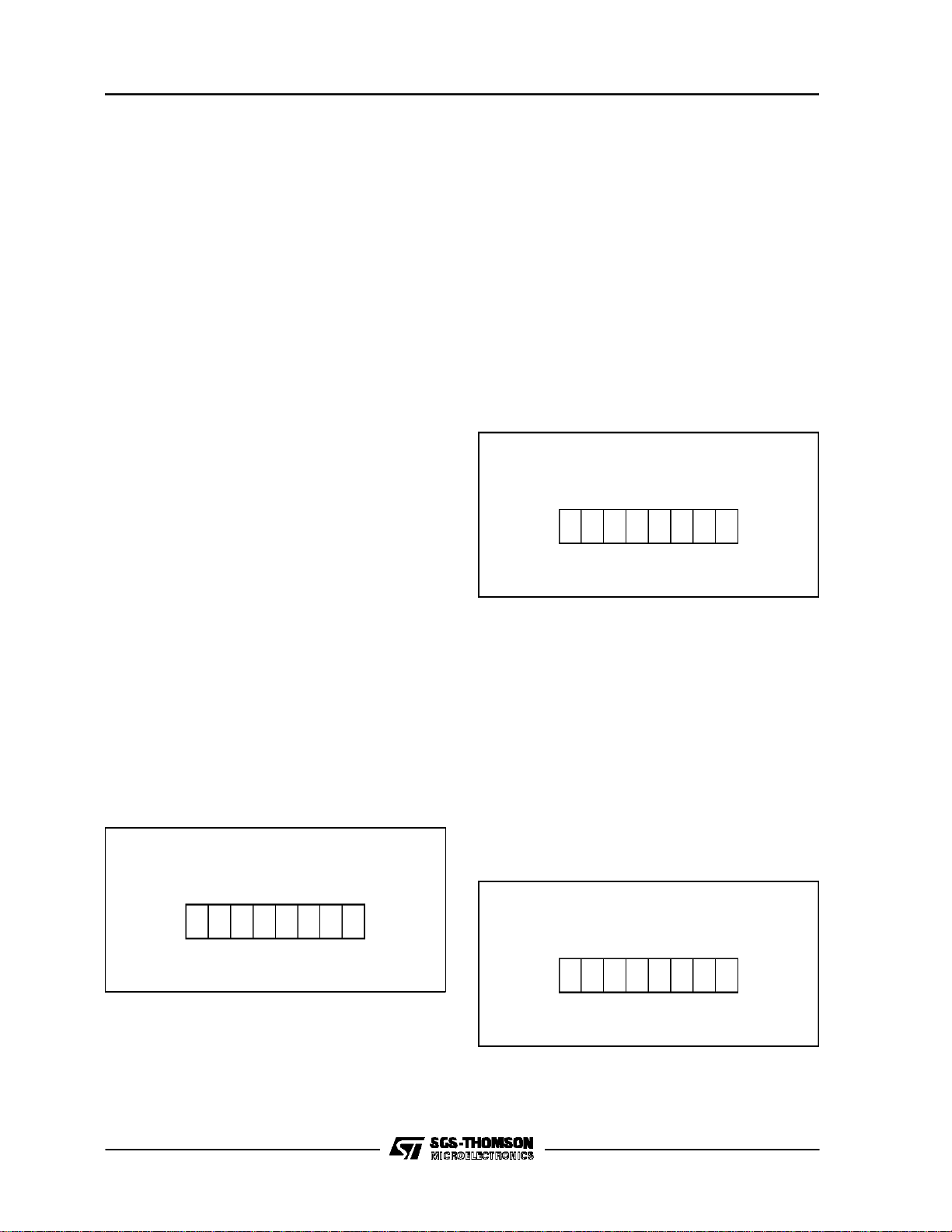
Figure8. Program ROMPage Register
PRPR
Program ROMPage Register
(CAh, Write Only)
D7 D6 D5 D4 D3 D2 D1 D0
ST6391,92,93,95,97,99
The DRBR can be addressedlike a RAMlocation
in the Data Space at the E8h address, nevertheless it is write-only register that can not be accessed with single-bit operations. This register is
used to select the desired 64-byteRAM/EEPROM
bank of the Data Space. The numberof the bank
has to be loaded inthe DRBR and the instruction
has to point to the selected location as itwas inthe
0 bank (from 00h address to 3Fh address). This
register is undefined afterReset. Refer to the Data
Space description for additional information. The
DRBRregisterisnot modifiedwhen a interruptor a
subroutine occurs.
Figure9. Data RAM Bank Register
DRBR
Data RAM Bank Register
(E8h, Write Only)
D7 D6 D5 D4 D3 D2 D1 D0
TheDRWR registercanbeaddressedlike a RAMlocationin theDataSpaceat the C9haddress,nevertheless it is write-only register that can not be
accessed with single-bit operations.This register is
used to move up and down the 64-byte read-only
datawindow (fromthe 40h addressto 7Fh address
of the Data Space)along the ROM of the MCU by
stepof 64 bytes.Theeffectiveaddressof thebyteto
bereadasadata inthe ROMisobtainedby the concatenationofthe6lesssignificantbitsoftheaddress
given in the instruction(as less significant bits)and
the contentof the DRWR (as most significantbits).
RefertotheDataSpacedescriptionforadditionalinformation.
Figure10. Data ROM Window Register
DRWR
Data ROM Window Register
(C9h, Write Only)
D7 D6 D5 D4 D3 D2 D1 D0
9/64
Page 14

ST6391,92,93,95,97,99
MEMORY SPACES
The MCUs operate in three different memory
spaces: Stack Space, Program Space, and Data
Space. A descriptionof these spaces is shown in
Figure 11.
Stack Space
Thestack spaceconsistsof six 12 bit registers that
areusedfor stackingsubroutineandinterrupt return
addressesplusthecurrentprogramcounterregister.
Program Space
The program space is physically implemented in
the ROM and includes all the instructions that are
to be executed, as well as the data requiredforthe
immediate addressing mode instructions, the reserved test area and uservectors. It is addressed
thanks to the 12-bit Program Counter register (PC
register) and so, the ST639x Core can directlyaddress upto 4K bytesof Program Space.Nevertheless, the ProgramSpace can be extended by the
addition of 2-KbyteROM banks as it is shown in
Figure 13 in which a 20K bytes memory is described.Thesebanks areaddressed bypointing to
the 000h-7FFh locations of the Program Space
thanks to the Program Counter, andby writingthe
appropriatecode in theProgram ROM Page Register (PRPR) located at the CAh address of the
Data Space.Becauseinterruptsand common subroutines should be available all the time only the
lower 2K byte of the 4K program space are bank
switched while the upper 2K byte can be seen as
static space. Table 3 gives thedifferent codes that
allows the selection of the corresponding banks.
Note that,fromthe memory point of view,thePage
1 and the StaticPage represent the same physical
memory:it isonly adifferentway ofaddressingthe
same location. On the ST6392,95,97, a total of
2048, bytes of ROM have been implemented;
20140 areavailableas userROMwhile 340arereservedfor testing.
Figure12. ST639x 20K Bytes Program Space
AddressingDescription
Program
counter
space
0FFFh
0800h
07FFh
0000h
0000h 4FFFh
Static Page
Page 1
Page 0
Page 1
Static Page
Page 9
Figure11. ST639x Memory Addressing Description Diagram
STACK SPACE
0000h
PROGRAM COUNTER
STACK LEVEL1
STACK LEVEL2
STACK LEVEL3
STACK LEVEL4
STACK LEVEL5
STACK LEVEL6
07FFh
0800h
0FF0h
0FFFh
PROGRAM SPACE
ROM
ROM
INTERRUPT &
RESET VECTORS
0-63
000h
03Fh
040h
070h
080h
081h
082h
083h
084h
0C0h
0FFh
DATA SPACE
RAM / E EPROM
BANKING AREA
DATA ROM
WINDOW
X RE GISTER
Y R EGISTER
V RE GISTER
WREGISTER
RAM
DATA ROM
WINDOW SELECT
DATA RAM
BANK SELECT
ACCUMULATOR
VR001568
10/64
Page 15
MEMORY SPACES(Continued)
Figure13. Program ROM Page Register
PRPR
Program ROMPage Register
(CAh, Write Only)
D7 D6 D5 D4 D3 D2 D1 D0
PRPR0
PRPR1
PRPR2
PRPR3
UNUSED
ST6391,92,93,95,97,99
interrupt driver in a (minor) part in the static page
(start and end), and in the second (major) part in
one dynamicpage. If it is impossible to avoid the
writing of this register in interrupts drivers, an image of this register must be saved in a RAMlocation, and eachtime theprogramwrites the PRPRit
writes also the image register.The image register
must be written first, so if an interruptoccurs between the two instructions the PRPR is not affected.
Table 3. ST639x ProgramROM Page Register
Coding
D7-D5. These bits are not used.
PRPR4-PRPR0. These are the program ROM
banking bits and thevalue loaded selects the corresponding page to be addressedin the lower part
of 4Kprogramaddress spaceas specifiedin Table
3. Thisregisteris undefined onreset.
Note. The number of bits implemented depends
on the size of the ROM of the device. Only the
lower part of address space has been bankswitched because interrupt vectors and common
subroutines should beavailable all the time. The
reason of this structure is due to the fact that it is
not possible to jump from a dynamic page to another, unless jumping back to the static page,
changingcontents of PRPR,and, than,jumping to
a differentdynamic page.
Care is required when handlingthe PRPR as it is
write only. For this reason, it is not allowed to
change the PRPR contents while executing interrupts drivers, as the driver cannot save and than
restore its previous content. Anyway, this operation may be necessaryif the sum ofcommonroutines and interrupt drivers will take more than 2K
bytes;in thiscase could benecessaryto dividethe
PRPR3 PRPR2 PRPR1 PRPR0 PC11
XXXX1
00000Page 0
00010
00100Page 2
00110Page 3
01000Page 4
01010Page 5
01100Page 6
01110Page 7
10000Page 8
10010Page 9
Memory
Page
Static
Page
(Page 1)
Page 1
(Static
Page)
11/64
Page 16

ST6391,92,93,95,97,99
MEMORY SPACES(Continued)
Table 4. ST639x Program ROM Map (up to 20K Bytes)
ROM Page Device Address Description
PAGE 0
PAGE 1
“STATIC”
PAGE 2
PAGE 3
PAGE 4
PAGE 5
PAGE 6
PAGE 7
PAGE 8
0000h-007Fh
0080h-07FFh
0800h-0F9Fh
0FA0h-0FEFh
0FF0h-0FF7h
0FF8h-0FFBh
0FFCh-0FFDh
0FFEh-0FFFh
0000h-000Fh
0010h-07FFh
0000h-000Fh
0010h-07FFh
0000h-000Fh
0010h-07FFh
0000h-000Fh
0010h-07FFh
0000h-000Fh
0010h-07FFh
0000h-000Fh
0010h-07FFh
0000h-000Fh
0010h-07FFh
Reserved
User ROM
User ROM
Reserved
Interrupt Vectors
Reserved
NMI Vector
Reset Vector
Reserved
User ROM
Reserved
User ROM
Reserved
User ROM
Reserved
User ROM
Reserved
User ROM
Reserved
User ROM (End of 16KST6391,93,99)
Reserved
User ROM
PAGE 9
12/64
0000h-000Fh
0010h-07FFh
Reserved
User ROM (End of 20KST6392,95,97)
Page 17

MEMORY SPACES(Continued)
Data Space
The instruction set of the ST639x Core operates on a specific space, named Data Space
that contains all the data necessary for the
processing of the program. The Data Spaceal-
ST6391,92,93,95,97,99
lows the addressing of RAM (256 bytes for the
ST639x family), EEPROM (up to 384 bytes),
ST639xCore/peripheralregisters,andread-only
datasuch asconstantsand thelook-uptables.
Figure14. ST639x Data Space
b7 b0
DATA RAM/EEPROM/OSD
BANK AREA
DATA ROM
WINDOW AREA
X REGISTER 080h
Y REGISTER 081h
V REGISTER 082h
W REGISTER 083h
DATA RAM
PORT ADATAREGISTER 0C0h
PORT BDATAREGISTER 0C1h
PORT CDATA REGISTER 0C2h
RESERVED 0C3h
PORT ADIRECTION REGISTER 0C4h
PORT BDIRECTION REGISTER 0C5h
PORT CDIRECTION REGISTER 0C6h
RESERVED 0C7h
INTERRUPT OPTION REGISTER 0C8h
DATA ROM WINDOW REGISTER 0C9h
PROGRAM ROM PAGE REGISTER 0CAh
RESERVED 0CBh
SPI DATAREGISTER 0CCh
RESERVED
TIMER 1PRESCALER REGISTER 0D2h
TIMER 1 COUNTER REGISTER 0D3h
TIMER1 STATUS/CONTROL REG. 0D4h
RESERVED
WATCHDOG REGISTER 0D8h
000h
03Fh
040h
07Fh
084h
0BFh
0CDh
0D1h
0D5h
0D7h
Figure15. ST639x Data Space (Continued)
b7 b0
RESERVED 0D9h
TIMER 2 PRESCALER REGISTER 0DAh
TIMER2 COUNTER REGISTER 0DBh
TIMER 2STATUSCONTROL REG. 0DCh
0DDh
RESERVED
0DFh
DA0 DATA/CONTROL REGISTER 0E0h
DA1 DATA/CONTROL REGISTER 0E1h
DA2 DATA/CONTROL REGISTER 0E2h
DA3 DATA/CONTROL REGISTER 0E3h
AFC, IR & OSD RESULT REGISTER 0E4h
OUTPUTS CONTROL REGISTER 0E5h
DA4 DATA/CONTROL REGISTER 0E6h
DA5 DATA/CONTROL REGISTER 0E7h
DATA RAM BANK REGISTER 0E8h
DEDIC. LATCHES CONTROL REG. 0E9h
EEPROMCONTROL REGISTER 0EAh
SPICONTROL REGISTER 1 0EBh
SPICONTROL REGISTER 2 0ECh
OSD CHARAC. BANK SELECT REG. 0EDh
0F0h
RESERVED
0FEh
ACCUMULATOR 0FFh
OSDCONTROLREGISTERSLOCATED
IN PAGE6 OFBANKED DATA RAM
VERTICAL START ADDRESS REG. 010h
HORIZONTALSTARTADDRESSREG. 011h
VERTICAL SPACE REGISTER 012h
HORIZONTAL SPACEREGISTER 013h
BACKGROUND COLOUR REGISTER 014h
GLOBAL ENABLEREGISTER 017h
13/64
Page 18

ST6391,92,93,95,97,99
MEMORY SPACES(Continued)
Data ROM Addressing. Allthe read-onlydata ar e
physic allyimplem entedin theROM inwhich theProgramSpaceisalsoimplemented.TheROMtherefore
containstheprogramto beexecutedandalsotheconstantsandthelook-uptablesneededforthe program.
Thelocat i onsofDataSpaceinwhichthedifferentconstants and look-up tables are addressed by the
ST639xCore can be considered as beinga 64-by t e
window throughwhich itis possi bl eto accessto the
read-onlydatastored in the ROM. This window is locatedfromthe40haddressto the7Fh addressin the
Data space and allowsthe directreadingofthebytes
from the 000h address to the 03Fh address in the
ROM.AllthebytesoftheROMcanbeusedtostore
eitherinstructi onsor read-onlydata. Indeed,thewindowcanbemovedbystepof64bytesalongtheROM
in writi ngthe appropr i atecodein the Write-onlyData
ROMWindowre gi s te r(DRW R, locationC9h).Theeffectiveaddressof the byte tobe read as a datain the
ROM is obtainedby the concatenationof the 6 less
significant bits of the address in the Data Space(as
lesssignifi c ant bits)and the contentoftheDRWR(as
most significant bits). So when addressing location
40hofdataspace,and 0 isloadedin the DRWR,the
physic aladdress edlocat i oninROMis00h.
Note. The dataROM window cannot addresswindows abovethe 16k byte range.
Figure17. Data ROM Window Memory Addressing
Figure16. Data ROM Window Register
DWR
Data ROMWindow Register
(C9h, Write Only)
D7 D6 D5 D4 D3 D2 D1 D0
DWR0 = Data ROMWindow 0
DWR1 = Data ROMWindow 1
DWR2 = Data ROMWindow 2
DWR3 = Data ROMWindow 3
DWR4 = Data ROMWindow 4
DWR5 = Data ROMWindow 5
DWR6 = Data ROMWindow 6
DWR7 = Data ROMWindow 7
DWR7-DWR0. These are the Data Rom Window
bits that correspond to the upper bits ofdata ROM
program space. This registeris undefinedafter reset.
Note.Careis requiredwhenhandlingtheDRWRas
it is write only. For this reason, it is not allowed to
change the DRWR contents while executing interruptsdrivers, as thedrivercannotsaveand thanrestoreits previouscontent.If it is impossibleto avoid
thewriting ofthisregisterininterruptsdrivers, animageofthisregistermustbesavedinaRAMlocation,
and each time the program writes the DRWR it
writes also the image register. The image register
must be written first, so if an interrupt occurs betweenthe two instructionsthe DRWRregister is not
affected.
DATA ROM
WINDOW REGISTER
CONTENTS
(DWR)
Example:
DWR=28h
ROM
ADDRESS:A19h
14/64
12
13
65432 0
7
0
0
11000000001
11
67891011
1
01
0
0000
0
1
543210
543210
1
0
1
00
11
PROGRAM SPACE ADDRESS
DATA SPACE ADDRESS
DATA SPACE ADDRESS
1
READ
40h-7Fh
IN INSTRUCTION
59h
VR01573B
Page 19
MEMORY SPACES(Continued)
ST6391,92,93,95,97,99
Data RAM/EEPROM/OSDRAM Addressing
InallmembersoftheST639xfamily64bytesofdata
RAMaredirectlyaddressableinthe dataspacefrom
80h to BFh addresses.The additional192 bytes of
RAM, the 384 bytes of EEPROM , and the OSD
RAM can be addressed using the banks of 64
bytes located between addresses 00h and 3Fh.
The selectionof the bank is done by programming
the Data RAM Bank Register (DRBR) located at
the E8h address of the Data Space. In this way
each bankofRAM,EEPROMorOSDRAMcan select 64 bytes at a time. No more than one bank
should beset at a time.
Figure18. Data RAMBank Register
DRBR
Data RAM
Bank Register
(E8h, Write Only)
D7 D6 D5 D4 D3 D2 D1 D0
DRBR0
DRBR1
DRBR2
DRBR3
DRBR4
DRBR5
DRBR6
DRBR7
DRBR7,DRBR1,DRBR0. These bits select the
EEPROM pages.
DRBR6, DRBR5.Each of these bits, when set,will
selectone OSDRAM register page.
DRBR4,DRBR3,DRBR2.Each of these bits,when
set,will select one RAM page.
This registeris undefined afterreset.
Table 5 summarizes how to set the Data RAM
Bank Register in order to select the various banks
or pages.
Note :
Care is required when handling the DRBR asit is
write only. For this reason, it is not allowed to
change the DRBR contentswhile executing interrupts drivers, as the driver cannot save and than
restore its previous content. If it is impossible to
avoid the writing of this register in interrupts drivers, an image of this register must be saved in a
RAM location, and each time the program writes
the DRBRit writes also the image register.
The image registermustbe written first,so if an interrupt occurs between the two instructions the
DRBR is not affected.
Table 5. Data RAMBank Register Set-up
DRBR Value
Hex. Binary
01h 0000 0001 EEPROM Page 0
02h 0000 0010 EEPROM Page 1
03h 0000 0011 EEPROM Page 2
81h 1000 0001 EEPROM Page 3
82h 1000 0010 EEPROM Page 4
83h 1000 0011 EEPROM Page 5
04h 0000 0100 RAM Page 2
08h 0000 1000 RAM Page 3
10h 0001 0000 RAM Page 4
20h 0010 0000 OSD Page 5
40h 0100 0000 OSD Page 6
Selection
All devices
ST6395 and ST6397
ONLY
All devices
15/64
Page 20
ST6391,92,93,95,97,99
MEMORY SPACES(Continued)
EEPROMDescription
The data space of ST639x family from 00h to 3Fh
is paged as described in Table 5. 384 bytes of
EEPROMlocated in sixpages of64 bytes (pages
0,1,2,3,4and 5, see Table 5).
Through the programmingof theData RAM Bank
Register (DRBR=E8h) the user can select the
bank or page leaving unaffected the way to address the static registers. The way to address the
“dynamic”page is tosetthe DRBRas described in
Table 5(e.g.toselectEEPROMpage 0,the DRBR
has to be loaded with content 01h, see Data
RAM/EEPROM/OSD RAM addressing for additional information).Bits 0, 1 and 7 of the DRBR are
dedicated tothe EEPROM.
The EEPROM pages do not require dedicated instructions to be accessedin readingor writing.The
EEPROM is controlled by the EEPROM Control
Register(EECR=EAh). AnyEEPROM locationcan
bereadjust likeanyotherdatalocation,alsointerms
ofaccesstime.
To write an EEPROM location takes an average
time of 5 ms (10ms max) and during this timethe
EEPROM is not accessible by the Core. A busy
flag canbe readby the Coretoknow the EEPROM
status before trying any access. In writing the
EEPROM can work in two modes: Byte Mode
(BMODE) and Parallel Mode (PMODE). The
BMODE is the normal way to use the EEPROM
and consistsin accessingone byte at atime. The
PMODE consists inaccessing 8 bytesper time.
Figure19. EEPROM Control Register
EECR
EEPROM Control Register
(EAh, Read/Write)
D7 D6 D5 D4 D3 D2 D1 D0
EN = EEPROMEnable Bit
BS = EEPROM Busy Bit
PE = Parallel Mode Enable Bit
PS = Parallel Start Bit
Reserved (Mustbe set Low)
Reserved (Mustbe set Low)
SB =Stand-by Enable Bit
Unused
D7. Not used
SB.WRITEONLY. Ifthis bit isset theEEPROMis
disabled(any accesswill bemeaningless)and the
power consumption of the EEPROMis reducedto
the leakage values.
D5, D4. Reserved for testingpurposes,they must
be setto zero.
PS.SET ONLY. Oncein Parallel Mode,assoon as
the usersoftwaresets the PSbitthe parallelwriting
of the 8 adjacentregisters will start.PSis internally
reset at the end of the programming procedure.
Note that less than 8 bytes can be written; after
parallel programming the remaining undefined
bytes will haveno particular content.
PE. WRITE ONLY. This bit must be set by the
user program in orderto performparallelprogramming (more bytes per time). If PE is set and the
“parallelstartbit”(PS)is low, upto 8adjacentbytes
can be writtenat the maximum speed, the content
being storedin volatileregisters.These 8 adjacent
bytes can be considered as row, whose A7, A6,
A5, A4, A3 are fixed while A2, A1 and A0 are the
changing bytes. PE is automatically reset at the
end of any parallel programming procedure. PE
can be reset by the user software before starting
the programming procedure, leaving unchanged
the EEPROMregisters.
BS.READ ONLY. This bitwill be automaticallyset
by the CORE when the user program modifies an
EEPROMregister. The user program hasto test it
before any read or write EEPROM operation; any
attemptto access the EEPROM while “busy bit” is
setwillbeabortedandthewriting procedureinprogress completed.
EN. WRITE ONLY.This bit MUSTbe set to one in
order to write any EEPROM register. If the user
program will attempt to write the EEPROM when
EN= “0” the involved registers will be unaffected
and the“busy bit”will notbe set.
AfterRESETthecontentofEECRregist erwi llbe 00h.
Notes :
When the EEPROM is busy (BS=“1”) the EECR
can notbe accessed inwrite mode, it is only possible to read BSstatus.This implies that as long as
the EEPROM is busy it is not possible to change
the status of the EEPROMcontrol register. EECR
bits 4 and 5 are reserved for test purposes, and
must never be set to “1”.
16/64
Page 21

ST6391,92,93,95,97,99
MEMORY SPACES(Continued)
Additional Notes on Parallel Mode. If the user
wants to perform a parallel programming the first
action should bethe set toone thePE bit; from this
moment the first time the EEPROM will be addressed in writing, the ROW address will be
latched and it will be possible to change it only at
the end ofthe programming procedureor byresetting PE without programming the EEPROM.After
the ROWaddress latching the Core can “see” just
one EEPROMrow (the selected one) and any attempt to write or read other rows will produceerrors. Donot read the EEPROMwhile PEis set.
As soon asPE bitis set,the 8volatile ROWlatches
are cleared. From this moment the user can load
data in the whole ROW or just in a subset.PS setting willmodify theEEPROM registerscorresponding to the ROW latches accessed after PE. For
example, if the software sets PE and accesses
EEPROM in writing at addresses18h,1Ah,1Bhand
thensetsPS,thesethreeregisterswillbemodifiedat
thesame time;the remainingbyteswill haveno particularcontent.NotethatPE isinternallyresetat the
endof theprogramming procedure.Thisimplies that
the user must set PE bit between two parallelprogrammingprocedures.Anywaytheusercansetand
thenresetPEwithoutperforminganyEEPROMprogramming.PS is a setonly bitand isinternallyreset
atthe end of the programmingprocedure.Notethat
if theusertriestosetPSwhilePEisnotsettherewill
not be any programming procedure and the PS bit
will be unaffected.ConsequentlyPS bitcan not be
setifENis low.PScanbeaffectedbytheusersetif,
andonlyif,ENand PE bits arealsosetto one.
INTERRUPT
The ST639x Core can manage 4 different maskable interrupt sources, plus one non-maskable interrupt source (top priority level interrupt). Each
sourceisassociated with aparticularinterruptvector that contains a Jump instruction to the related
interrupt serviceroutine. Each vector is located in
the Program Space at a particular address (see
Table 6). When a source provides an interruptrequest, and therequest processingis alsoenabled
by the ST639x Core,then thePCregisterisloaded
with the address of the interrupt vector (i.e.of the
Jumpinstruction).Finally,the PCis loaded withthe
address of the Jump instruction and the interrupt
routine is processed.
The relationship between vector and source and
the associatedpriority ishardware fixed for the differentST639xdevices. Forsome interrupt sources
it is also possible to select by software the kind of
event that will generatethe interrupt.
All interruptscan be disabled by writing to theGEN
bit (global interruptenable) of the interrupt option
register (address C8h). Aftera reset,ST639x is in
non maskable interruptmode, so no interrupts will
be accepted and NMI flags will be used, until a
RETI instruction is executed.If an interruptis executed, one special cycle is made by the core,during that the PC is set to the related interrupt vector
address. A jump instructionat thisaddress has to
redirect program execution to thebeginningof the
relatedinterruptroutine.Theinterruptdetectingcycle, also resets the relatedinterrupt flag(not available to the user), so that another interrupt can be
stored for this current vector, while its driver is under execution.
If additionalinterruptsarrivefromthe same source,
they will be lost. NMI can interrupt other interrupt
routines at any time,while other interrupts cannot
interrupt each other. If more than one interrupt is
waiting forservice, they are executed according to
their priority. The lower the number, the higher the
priority. Priority is, therefore, fixed. Interrupts are
checked during the last cycle of an instruction
(RETIincluded). Level sensitive interrupts have to
be validduring this period.
17/64
Page 22

ST6391,92,93,95,97,99
INTERRUPT(Continued)
Table 6. Interrupt Vectors/Sources
Relationships
Interrupt Source
PC6/IRIN
(1)
Pin
Timer 2
Vsync
Timer 1
PC4/PWRIN
Note 1. This pin isassociated withthe NMI Interrupt Vector
Associated
Vector
Interrupt
Vector # 0 (NMI)
Interrupt
Vector # 1
Interrupt
Vector # 2
Interrupt
Vector # 3
Interrupt
Vector # 4
Vector Address
0FFCh-0FFDh
0FF6h-0FF7h
0FF4h-0FF5h
0FF2h-0FF3h
0FF0h-0FF1h
InterruptOption Register
The Interrupt Option Register (IOR register, location C8h) is used to enable/disable the individual
interrupt sources and to select the operating mode
of theexternal interrupt inputs.Thisregistercanbe
addressed in the Data Space as RAM location at
the C8h address,nevertheless it is write-only register that can not be accessed with single-bit operations. The operating modes of the external
interrupt inputs associated to interruptvectors #1
and #2are selectedthrough bits4 and5 of theIOR
register.
Figure20. InterruptOption Register
IOR
InterruptOption Register
(C8h, Write Only)
InterruptVectors/Sources
The ST639x Core includes 5 different interrupt
vectors in order to branch to 5 different interrupt
routines. The interrupt vectors are located in the
fixed (or static)page of the Program Space.
The interruptvectorassociatedwith thenon-maskable interrupt source is named interrupt vector#0.
It is located at the (FFCh,FFDh) addresses in the
Program Space.This vectoris associatedwith the
PC6/IRINpin.
The interrupt vectors located at addresses
(FF6h,FF7h), (FF4h,FF5h), (FF2h,FF3h),
(FF0h,FF1h) are named interrupt vectors #1, #2,
#3 and #4respectively.These vectorsare associated with TIMER 2 (#1), VSYNC (#2), TIMER 1
(#3) and PC4(PWRIN)(#4).
InterruptPriority
The non-maskable interrupt request has the highest priority and can interrupt any other interrupt
routines at any time, nevertheless the other interrupts cannot interrupteach other. Ifmore than one
interrupt requestis pending,they areprocessedby
the ST639x Core according to their priority level:
vector#1 has the higherprioritywhile vector#4the
lower. Thepriority of each interrupt sourceis hardware fixed.
D7 D6 D5 D4 D3 D2 D1 D0
Unused
GEN = Global EnableBit
ES2 = Edge SelectionBit
EL1 = EdgeLevelSelection Bit
Unused
D7. Not used.
EL1. This is the Edge/Level selection bit of inter-
rupt#1.When set to one,the interruptisgenerated
on low level of the related signal; when cleared to
zero,the interruptisgenerated on falling edge.The
bit iscleared to zero after reset.
ES2. This is the edge selection bit on interrupt#2.
This bit is used on the ST639xdeviceswithon-chip
OSDgenerator for VSYNC detection.
GEN.Thisis theglobalenablebit.Whensetto oneall
interruptsareglobally enabl ed;whenthis bitiscleared
tozero all interruptsaredisabl ed(excl udi ngNM I).
D3 - D0. Thesebits are not used.
18/64
Page 23

INTERRUPT(Continued)
InterruptProcedure
The interruptprocedure is verysimilar to a callprocedure; the user can consider the interruptas an
asynchronous call procedure. As this is an asynchronous event the user does notknow about the
context and thetime at which itoccurred. As a result the user should save all thedata space registers whichwill be usedinsidetheinterruptroutines.
There are separatesets of processor flags for normal, interrupt and non-maskable interrupt modes
which are automaticallyswitched and so these do
not need to be saved.
The following list summarizes the interruptprocedure (refer also to Figure 21. Interrupt Processing
Flow Chart):
Interrupt detection
-
The flags C and Z of the main routine are ex-
-
changed with the flags C and Z of the interrupt
routine (resp.the NMIflags)
The valueof thePC is storedin the firstlevel of
-
the stack- The normalinterrupt lines are inhibited (NMI still active)
The edgeflip-flop is reset
-
The relatedinterrupt vectoris loaded inthe PC.
-
User selected registers are saved insidethe in-
-
terrupt service routine (normally on a software
stack)
The source of the interrupt is found by polling
-
(if more than one source is associated to the
same vector)
Interrupt servicing
-
Return from interrupt (RETI)
-
Automatically the ST639x core switches back
-
to the normal flags (resp the interrupt flags)
and popsthe previous PC value fromthe stack
The interruptroutine begins usually by the identification of the device that has generated the interrupt request. The user should save the registers
which are used inside the interrupt routine (that
holds relevantdata) intoa software stack.
Afterthe RETIinstruction execution,the Core carries out theprevious actions and themain routine
can continue.
ST6391,92,93,95,97,99
Figure21. InterruptProcessingFlow-Chart
INSTRUCTION
FETCH
INSTRUCTION
EXECUTE
INSTRUCTION
WAS
THE INSTRUCTION
ARETI
YES
YES
NO
?
NO
CLEAR
INTERRUPT MASK
SELECT
PROGRAM FLAGS
” POP ”
THE STACKED PC
?
ST639x InterruptDetails
IR Interrupt (#0). The IRIN/PC6 Interrupt is con-
nected to the firstinterrupt #0 (NMI,0FFCh). If the
IRINT interrupt is disabled at the Latch circuitry,
then it will be high. The #0interrupt inputdetectsa
high to low level. Note that once #0 has been
latched, then the only way to remove the latched
#0 signal isto servicetheinterrupt.#0 caninterrupt
the otherinterrupts.A simple latchisprovidedfrom
the PC6(IRIN) pin in order to generate the IRINT
signal. This latch can be triggered by either the
positive or negative edge of IRIN signal.IRINT is
inverted with respect to the latch. The latch can be
read bysoftware and resetby software.
NO
IS THE CORE
ALREADY IN
NORMAL MODE ?
CHECK IF THERE IS
AN INTERRUPT REQUEST
AND INTERRUPT MASK
YES
LOAD PC FROM
INTERRUPT VECTOR
( FF C / FFD )
SET
INTERRUPT MASK
PUSH THE
PC INTO THE STACK
SELECT
INTERNAL MODE FLAG
VA000014
19/64
Page 24

ST6391,92,93,95,97,99
INTERRUPT(Continued)
TIMER 2 Interrupt (#1). The TIMER 2 Interrupt is
connectedto theinterrupt #1 (0FF6h).TheTIMER2
interruptgeneratesalowlevel(whichislatchedinthe
timer) .Onl ythelow leve lselectio nfor#1 can be used.
Bit6oftheinterruptoptionregis terC8hhas to be set.
VSYNC Interrupt (#2). The VSYNC Interrupt is
connected to the interrupt #2. When disabled the
VSYNCINTsignal islow.TheVSYNCINTsignalis
inverted with respect to the signal applied to the
VSYNC pin. Bit 5 of the interrupt option register
C8h isusedtoselectthenegative edge (ES2=0)or
the positive edge (ES2=1);the edge will depend
on the application. Note that once an edge has
been latched, then the only way to remove the
latched signal is to servicetheinterrupt.Care must
be taken notto generate spurious interrupts. This
interrupt may be used for synchronize to the
VSYNCsignal in order to change charactersin the
OSD only when the screen is on verticalblanking
(if desired). This method may also be used to blink
characters.
TIMER 1 Interrupt(#3). The TIMER 1 Interruptis
connected to the fourth interrupt#3 (0FF2h) which
detectsa low level(latched in the timer).
PWR Interrupt (#4). The PWR Interrupt is connected to the fifth interrupt #4 (0FF0h). If the
PWRINT is disabled at the PWR circuitry, then it
will be high. The #4 interrupt input detects a low
level. A simple latch is provided from the PC4
(PWRIN)pinin order to generate the PWRINT signal. This latch can be triggered by either thepositive or negative edge of the PWRIN signal.
PWRINT is inverted with respectto the latch. The
latch can be reset by software.
Notes Global disable does not reset edge sensitive interruptflags. These edge sensitive interrupts
becomependingagainwhenglobaldisablingis released. Moreover, edge sensitive interrupts are
stored in therelated flags also when interrupts are
globallydisabled,unlesseachedge sensitiveinterrupt is also individually disabled before the interrupting event happens. Global disable is done by
clearing the GEN bit of Interrupt option register,
while any individual disable is done in the control
register of the peripheral. The on-chip Timer peripheralshavean interruptrequestflagbit(TMZ ), this
bit isset to onewhenthedevicewantsto generatean
interruptrequestandama skbit(ETI)thatmustbeset
tooneto allowthe transferof theflagbit totheCore.
20/64
Page 25

RESET
TheST639xdevicescanberesetintwoways:bythe
external reset input (RESET) tied low and by the
hardwareactivateddigitalwatchdogperipheral.
RESETInput
Theexternal activelow reset pinisusedtoresetthe
ST638x devices and provide an orderly software
startup procedure. The activation of the Reset pin
may occurat any time in the RUN or WAIT mode.
Even short pulsesat the reset pin will be accepted
sincetheresetsignalislatchedinternallyandisonly
cleared after 2048 clocks at the oscillator pin. The
clocksfromtheoscillatorpintotheresetcircuitryare
bufferedby a schmitt triggerso that an oscillator in
start-up conditions will not give spurious clocks.
Whenthereset pinisheldlow, the ex ternalcrystaloscillatoris also disabl edin orderto reducecurrent consumption.TheMCUis configuredinthe Resetmode
as lo ng as the signal of the RESET pin is low. The
processi ngoftheprogramisstoppedandthestandard
Input/Outputports(portA,portB andportC) areinthe
input state. As soonas the levelonthe reset pi n becomes high, the initializa tion sequenc eis executed.
RefertotheMCU initiali z ati onsequenceforadditi onal
information.
ST6391,92,93,95,97,99
WatchdogReset
The ST639x devices are provided with an on-chip
hardware activateddigital watchdogfunction inorder to providea graceful recovery from a software
upset.Ifthe watchdog registeris not refreshed and
the end-of-count is reached, then the reset state
will be latched into the MCU andan internalcircuit
pulls down the reset pin. This also resets the
watchdog which subsequently turns off the pulldown and activates thepull-up device at thereset
pin. This causes the positivetransition at the reset
pin. The MCU will then exit the reset state after
2048 clockson the oscillator pin.
ApplicationNotes
An external resistorbetweenV
is not requiredbecausean internal pull-up device
is provided.Theusermay prefer to addan external
pull-up resistor.
An internal Power-on device does notguarantee
that the MCU will exit the reset state when V
above 4.5V and therefore the RESET pin should
be externallycontrolled.
andthe reset pin
DD
DD
is
Figure22. Internal Reset Circuit
OSCILLATOR
SIGNAL
RESET
(ACTIVE LOW)
1.0k
V
DD
300k
TO ST6
WATCHDOG RESET
RESET
ST6
INTERNAL RESET
COUNTER
VA000200
21/64
Page 26

ST6391,92,93,95,97,99
RESET(Continued)
Figure23. Reset & Interrupt Processing
Flow-Chart
RESET
NMI MASK SET
INT LATCH CLEARED
( IF PRESENT )
SELECT
NMI MODE FLAGS
PUT FFEh
ON ADDRESS BUS
YES
IS RESET
STILL PRESENT ?
NO
LOAD PC
FROM RESET LOCATIONS
FFE / FFF
FETCH INSTRUCTION
VA000427
Figure24. Restart InitializationProgram
Flow-Chart
RESET
RESET VECTOR
INITIALIZATION
ROUTINE
JP
RETI
JP: 2 BYTES/4 CYCLES
RETI: 1BYTES/2 CYCLES
VA000181
MCU InitializationSequence
When a resetoccurs the stack is resetto program
counter, the PC is loaded with the address of the
reset vector (located in the program ROM at addresses FFEh & FFFh). A jump instruction to the
beginning of the program has to be written into
these locations. After a reset the interrupt maskis
automatically activated so that the Coreis in nonmaskable interruptmode to prevent false or ghost
interrupts during the restartphase. Therefore the
restart routine should be terminatedby a RETI instruction to switch to normalmode and enable interrupts. If no pending interrupt is present at the
end ofthe reset routine, the ST639x will continue
with the instruction after the RETI; otherwise the
pendinginterrupt will be serviced.
RESETLow Power Mode
(ST6392 and ST6399 only)
When the reset pin is low, the quartz oscillator is
Disabled allowing reduced current consumption.
When the reset pin is raisedthe quartzoscillator is
enabled and oscillations will start to build up.The
internal resetcircuitrywill count 2048clocks on the
oscillator pin before allowingthe MCUto go out of
the resetstate;the clocksareaftera schmitt trigger
so thatfalse or multiple counts arenot possible.
22/64
Page 27

WAIT & STOPMODES
The STOP and WAIT modes have been implemented in the ST639x Core in order to reduce the
consumption of the device when the latter has no
instruction to execute. These two modes are described in the followingparagraphs.OnST639x as
the hardwareactivateddigital watchdog functionis
present the STOPinstruction is de-activated and
any attempt to execute it will cause the automatic
execution ofa WAIT instruction.
WAIT Mode
Theconfigurationofthe MCUintheWAITmodeoccurs as soon as the WAIT instruction is executed.
Themicrocontrollercan alsobeconsideredasbeing
in a “software frozen” state where the Core stops
processing the instructions of the routine, the contents of the RAM locationsand peripheralregisters
are saved as long as the power supply voltage is
higherthantheRAMretentionvoltagebutwherethe
peripheralsarestill working.
TheWAITmode is usedwhen the userwantsto reducetheconsumptionof theMCU when it isin idle,
whilenot losingcountof time or monitoringofexternal events. The oscillator is not stoppedin order to
provide clock signal to the peripherals.The timers
counting may be enabled (writing the PSI bit in
TSCRregister)and the timer interrupt may be also
enabledbeforeenteringtheWAITmode;this allows
the WAIT mode to be left when timer interrupt occurs. If the exit from the WAIT mode is performed
witha generalRESET(either from the activation of
the externalpin or by watchdogreset)the MCU will
enter a normalreset procedureas describedin the
RESETchapter. If an interrupt is generated during
WAIT mode the MCU behaviour depends on the
state of theST639xCore before theinitializationof
the WAITsequence, but also of the kind ofthe interrupt requestthat is generated. This case will be
described in the followingparagraphs.In any case,
the ST639x Core does notgenerateany delay after the occurrenceof the interrupt because the oscillator clockis still available.
STOP Mode
On ST639xthe hardware watchdogis present and
the STOPinstruction has been de-activated. Any
attemptto executea STOPwill causetheautomatic executionof aWAIT instruction.
Exit from WAIT Mode
The following paragraphsdescribe the outputprocedure ofthe ST639x CorefromWAITmode when
an interruptoccurs.Itmust benotedthat the restart
sequence depends on the original state of the
ST6391,92,93,95,97,99
MCU (normal, interrupt or non-maskableinterrupt
mode) before the startof the WAIT sequence, but
also ofthe type of the interrupt request that is generated.In all casesthe GENbitof IORhas tobe set
to 1 in order to restartfrom WAIT mode. Contrary
to the operation of NMI in the RUN mode, the NMI
is maskedinWAIT mode if GEN=0.
Normal Mode. If theST639xCorewas in themain
routinewhentheWAITinstructi onhasbeenexecuted,
theST6398xCor eoutputsfromthewaitmodeassoon
asany interrupt occurs ;the rel atedinterr uptroutineis
executedandattheendoftheinterruptserviceroutine
theinstructi onthatfoll owstheWAITinstr uctionisexecutedif no otherinterruptsarepending.
Non-maskable Interrupt Mode. If the WAIT instruction has been executedduring the execution
of the non-maskable interruptroutine, the ST639x
Core outputs from the wait modeas soon as any
interrupt occurs: the instruction that follows the
WAITinstructionis executedand the ST639xCore
is still in the non-maskableinterrupt mode even if
another interrupthas been generated.
Normal Interrupt Mode. If the ST639x Core was
in the interruptmode beforethe initialization of the
WAITsequence, it outputsfrom the wait mode as
soon as any interrupt occurs. Nevertheless, two
caseshave to be considered:
– If the interrupt is a normal interrupt, the inter-
ruptroutinein whichthe WAITwas enteredwill
be completedwith the execution of the instruction that follows the WAIT and the ST639x
Core isstill in the interruptmode. Atthe endof
this routine pending interruptswill beserviced
in accordanceto their priority.
– If the interrupt is a non-maskable interrupt,the
non-maskable routine is processed at first.
Then, the routine in which the WAIT was entered will be completed with the execution of
the instruction that follows the WAIT and the
ST639x Core is still in the normal interrupt
mode.
Notes :
If all theinterrupt sources are disabled,the restart
of theMCU canonlybedone bya Resetactivation.
The Wait instruction is not executed if an enabled
interrupt request is pending. In the ST639x the
hardware activated digital watchdog function is
present. As the watchdog is always activated the
STOP instruction is de-activated and any attempt
to executethe STOP instructionwill cause an execution of a WAITinstruction.
23/64
Page 28

ST6391,92,93,95,97,99
ON-CHIPCLOCK OSCILLATOR
The internal oscillator circuit is designed to require
a minimum of external components. A crystal
quartz, a ceramicresonator, or an external signal
(provided tothe OSCin pin) maybe used to generate a systemclockwith various stability/costtradeoffs. The typical clock frequency is 8MHz. Please
notethat differentfrequencieswi ll affectthe operation
of thoseperipherals(D/As, SPI)whosereferencefrequenciesarederivedfromthesystemclock.
The different clock generator options connection
methodsare shownin Figures25 and 26.One machine cycle takes 13 oscillator pulses; 12 clock
pulses are needed to increment the PC while and
additional13thpulseis neededto stabilizetheinternal latchesduringmemoryaddressing.This means
thatwith a clockfrequencyof 8MHz the machinecycle is 1.625µs.
The crystal oscillator start-up time is a function of
manyvariables:crystal parameters(especially RS),
oscillatorloadcapacitance(CL),ICparameters,ambienttemperature,andsupplyvoltage.Itmustbeobservedthat the crystalor ceramic leads and circuit
connections must be as short as possible. Typical
valuesforCL1 andCL2 are in therangeof 15pFto
22pFbuttheseshouldbechosenbasedon thecrystalmanufacturersspecification.Typical inputcapacitanceforOSCin andOSCoutpinsis5pF.
The oscillatoroutputfrequencyis internallydivided
by 13 to produce the machine cycle and by 12 to
produce theTimerand the Watchdogclock.A byte
cycle is the smallest unit neededto execute any
operation (i.e.,incrementthe program counter).An
instruction may need two, four, or five byte cycles
to beexecuted (See Table 7).
Figure25. Clock GeneratorOption(1)
Figure26. Clock GeneratorOption(2)
Table 7. IntructionsTimingwith 8MHz Clock
Instruction Type Cycles
Branch if set/reset 5 Cycles 8.125µs
Branch & SubroutineBranch 4 Cycles 6.50µs
Bit Manipulation 4 Cycles 6.50µs
Load Instruction 4 Cycles 6.50µs
Arithmetic & Logic 4 Cycles 6.50µs
Conditional Branch 2 Cycles 3.25µs
Program Control 2 Cycles 3.25µs
24/64
Execution
Time
Figure27. OSCin,OSCout Diagram
Page 29

INPUT/OUTPUT PORTS
The ST639x microcontrollers use three standard
I/Oports (A,B,C)withup to eightpinson each port;
refer to the devicepin configurationsto see which
pins areavailable.
Each linecan beindividuallyprogrammed eitherin
the input mode or the output mode as follows by
software.
- Output
- Input with on-chip pull-up resistor (selectedby
software)
- Input without on-chip pull-up resistor(selected
by software)
Note: pins with 12V open-drain capability do not
have pull-upresistors.
In output mode the following hardware configurations are available:
- Open-drain output 12V (PA4-PA7,PC4-PC7)
- Open-drain output 5V (PC0-PC3)
- Push-pull output (PA0-PA3,PB0-PB6)
The lines areorganizedinthree ports(portA,B,C).
The ports occupy 6 registers in the data space.
Each bitof theseregistersis associated with a particular line (for instance, the bits 0 of the Port A
Data and Direction registers are associated with
the PA0line of Port A).
There arethree Data registers(DRA,DRB, DRC),
that are used toread thevoltage level valuesof the
lines programmedin the inputmode, or towrite the
logic value of the signal to be output on the lines
configured inthe outputmode.The port DataRegisters canbe read togetthe effectivelogiclevels of
the pins,but they can be also writtenby the user
software, in conjunction with the related Data Direction Register,to select the differentinput mode
options. Single-bit operations on I/O registers (bit
set/resetinstructions)are possible but care is necessary because reading in input mode is made
from I/Opins and therefore might be influenced by
the external load, while writing will directly affect
the Port data register causing an undesired
changes of the input configuration. The threeData
Direction registers (DDRA, DDRB, DDRC) allow
the selectionof the direction of each pin (input or
output).
All theI/O registers can be read or written as any
other RAM location of the dataspace, so no extra
RAM cell is needed for port data storing and manipulation. During the initialization of the MCU, all
the I/O registers are cleared and the input mode
with pull-upis selected on all the pinsthusavoiding
pin conflicts(withtheexceptionofPC2 thatisset in
output modeand is set high ie. highimpedance).
ST6391,92,93,95,97,99
Details of I/O Ports
Whenprogrammedas an input a pull-up resistor (if
available) can be switched active under program
control. When programmed as an output the I/O
port will operate either in thepush-pullmode orthe
open-drainmode according to the hardware fixed
configuration as specifiedbelow.
Port A. PA0-PA3are available as push-pullwhen
outputs. PA4-PA7are available as open-drain (no
push-pull programmability) capable of withstanding 12V(no resistivepull-up in input mode). PA6PA7 hasbeen speciallydesignedforhigher driving
capability and are able to sink 25mA with a maximum V
Port B. All lines are configured as push-pullwhen
outputs.
Port C. PC0-PC3 are available as open-draincapable ofwithstanding a maximum V
PC7 are available as open-drain capable of
withstanding 12V (no resistive pull-up in input
mode).Some lines are also usedas I/Obuffersfor
signals coming fromthe on-chip SPI.
In this case the final signal on the output pin is
equivalent to a wired AND with the programmed
data output.
If the user needs to use the serial peripheral, the
I/O line should be set in output mode while the
open-drain configuration is hardware fixed; the
corresponding data bit must set to one. If the
latchedinterruptfunctionsare used(IRIN,PWRIN)
then the corresponding pins should be set to input
mode.
On ST639x the I/O pins with double or special
functionsare:
- PC0/SCL (connectedto the SPI clock signal)
- PC1/SDA (connected tothe SPI data signal)
- PC3/SEN(connectedtotheSPIenablesignal)
- PC4/PWRIN (connected to the PWRIN inter-
- PC6/IRIN (connected to the IRIN interrupt
All the PortA,B and C I/O lines have Schmitt-trigger input configurationwith a typical hysteresisof
1V.
of1V.
OL
rupt latch)
latch)
+0.3V.PC4-
DD
25/64
Page 30

ST6391,92,93,95,97,99
INPUT/OUTPUT PORTS (Continued)
Table 8. I/O Port Options Selection
DDR DR Mode Option
0 0 Input
0 1 Input Without on-chip pull-up resistor
1 X Output Open-drain orPush-Pull
Note: X: Means don’tcare.
With on-chip pull-up
resistor
I/O Pin Programming
Eachpincanbe individuallyprogrammedasinputor
outputwith differentinputandoutputconfigurations.
This isachieved by writing to the relevant bit in the
data (DR)and datadirection register(DDR). Table
8 shows all the port configurations that can be selected by the user software.
Figure29. Port A, B, CData Register
Figure28. Port A, B, CData Register
DRA, DRB, DRC
Port A, B, C Data Register
( C0hPA, C1h PB,C2h PCRead/ Write )
D7 D6 D5 D4 D3 D2 D1 D0
A0 - PA7 = Data Bits
PB0 - PB7 =Data Bits
PC0 - PC7 = Data Bits
PA7-PA0.Thesearethe I/O portAdatabits. Reset
at power-on.
PB7-PB0.These arethe I/Oport B data bits.Reset
at power-on.
PC7-PC0. Set to 04h at power-on. Bit 2 (PC2 pin)
is set to one (open drain therefore high impedence).
DDRA, DDRB,DDRC
Port A, B, CData Direction Register
( C4h PA, C5h PB, C6h PCRead/ Write )
D7 D6 D5 D4 D3 D2 D1 D0
PA0 - PA7 =Data Direction Bits
PB0 - PB7 =Data Direction Bits
PC0 - PC7 = Data DirectionBits
“0” Defines bitas Inpu t
”1” Defines bitas Output
PA7-PA0. These are the I/O port A data direction
bits. When a bit is cleared to zero the related I/O
line is in input mode, if bit is setto one the related
I/Oline is in output mode. Reset atpower-on.
PB7-PB0. These are the I/Oport B data direction
bits. When a bit is cleared to zero the related I/O
line is in input mode, if bit is setto one the related
I/Oline is in output mode. Reset atpower-on.
PC7-PC0. These are the I/Oport C datadirection
bits. When a bit is cleared to zero the related I/O
line is in input mode, if bit is setto one the related
I/Oline is inoutput mode. Set to 04h at power-on.
Bit 2 (PC2 pin) is set to one (output mode selected).
26/64
Page 31

INPUT/OUTPUT PORTS (Continued)
Input/Output Configurations
The following schematics show the I/Olines hardware configuration for the different options. Figure
30 shows the I/Oconfiguration for an I/O pin with
open-drain 12Vcapability(standard drive and high
drive). Figure 31 shows the I/Oconfiguration foran
I/Opin with push-pull and with opendrain5Vcapability.
Figure30. I/O Configuration Diagram
(Open Drain 12V)
ST6391,92,93,95,97,99
Notes :
The WAIT instruction allows the ST639x to be
used insituationswhere lowpower consumptionis
needed. This can only be achievedhowever if the
I/Opins either are programmed asinputs with well
defined logic levels or have no power consuming
resistive loads in output mode.As the same die is
used forthe differentST639x versions theunavailable I/Olines of ST639x should be programmedin
output mode.
Single-bit operations on I/O registers are possible
but care is necessary because reading in input
mode is made from I/O pins while writing will directlyaffectthe Portdataregistercausingan undesired changes of the input configuration.
Figure31. I/O Configuration Diagram (Open Drain 5V, Push-pull)
27/64
Page 32

ST6391,92,93,95,97,99
TIMERS
TheST639xdevicesoffertwoon-chipTimerperipherals consistingof an 8-bitcounter with a 7-bitprogrammableprescaler, thusgiving amaximum count
15
,and a controllogicthat allowsconfiguringthe
of2
peripheral operating mode. Figure 32 shows the
timerblock diagram.The contentof the 8-bitcounters can be read/writtenin the Timer/Counter registersTCRthatcanbeaddressedinthedataspaceas
RAMlocation ataddressesD3h (Timer 1) and DBh
(Timer 2). The state of the 7-bit prescaler can be
readin thePSCregisterataddressesD2h (Timer1)
andDAh(Timer 2). Thecontrollogicis managedby
TSCRregistersat D4h(Timer 1)and DCh (Timer 2)
addressesas describedin thefollowingparagraphs.
The following description applies to both Timer 1
and Timer2. The 8-bit counter isdecrement by the
output (rising edge) coming from the 7-bit prescaler and can be loaded and read under program
control. When it decrements to zero then theTMZ
(timer zero) bit in the TSCR is set to one. If the ETI
(enable timerinterrupt) bit in the TSCRis also set
to one an interruptrequest, associatedto interrupt
vector#3 (forTimer1) and #1for Timer2, isgenerated. The interruptof the timer can be usedto exit
the MCUfrom the WAIT mode.
The prescaler decrements on rising edge. The
prescaler input is the oscillator frequencydivided
by 12.
Depending on the division factor programmed by
PS2/PS1/PS0(see Table 9) bits in the TSCR, the
clock input of the timer/counter register is multiplexed todifferentsources.
Ondivisi onfactor1, the clockinputof the presc al eris
alsothatoftimer/counter;on factor2,bit0ofprescaler
regis terisconnectedto the clockinputof TCR .
This bitchanges its statewith the halffrequencyof
prescaler clock input.On factor 4, bit 1 of PSC is
connectedto clockinput ofTCR, and so on. Ondivision factor 128, the MSB bit 6 of PSC is connected to clock input of TCR. The prescaler
initialize bit (PSI)in the TSCRregister mustbe set
to one to allow the prescaler (and hence the
counter) to start. If it is cleared to zero then all of
the prescalerbits are set to one and the counter is
inhibited fromcounting.
The prescaler can be given any value between 0
and 7Fh by writingto the relatedregister address,
if bitPSIin theTSCR register isset to one. Thetap
oftheprescalerisselectedusingthePS2/PS1/PS0
bits in the control register. Figure 33 shows the
timerworking principle.
Figure32. Timer Peripheral Block Diagram
28/64
Page 33

TIMERS(Continued)
Figure33. Timer Working Principle
ST6391,92,93,95,97,99
Timer OperatingModes
AsonST639xdevicestheexternalTIMERpin isnot
availabletheonlyallowedoperatingmodeistheoutput modethathaveto beselectedby setting to1bit
4 andby clearing to 0 bit 5 in the TSCR1 register.
ThisprocedurewillenablebothTimer1 andTimer2.
OutputMode(TSCR1 D4 = 1, TSCR1 D5= 0). On
this mode the timer prescaler is clocked by the
prescaler clock input (OSC/12). The user can select thedesired prescaler divisionratio through the
PS2/PS1/PS0bits. WhenTCR count reaches 0, it
sets the TMZbit in theTSCR.
The TMZ bit canbe testedunder program control
to performtimer functions whenever it goes high.
Bit D4and D5on TSCR2(Timer 2) register are not
implemented.
Timer Interrupt
When thecounter registerdecrementsto zero and
the softwarecontrolled ETI(enable timer interrupt)
bit is set to one then an interrupt request associated tointerruptvector#3 (forTimer1)and tointerrupt vector #1 (forTimer2) is generated.When the
counter decrementsto zero also the TMZ bit in the
TSCR registeris set to one.
Notes :
TMZ is set when the counter reaches 00H ; however,it may be set bywriting 00Hin the TCR register or setting the bit 7 of the TSCR register. TMZ
bit must be cleared by user software when servicing thetimer interruptto avoid undesired interrupts
when leavingthe interruptserviceroutine. After reset,the 8-bitcounterregisterisloadedto FFhwhile
the 7-bitprescaler isloaded to 7Fh , andthe TSCR
register is cleared which means that timer is
stopped (PSI=0)and timer interruptdisabled.
A write to the TCR register will predominate over
the 8-bitcounterdecrementto 00h function,i.e. if a
write and a TCR register decrementto 00h occur
simultaneously,the write will takeprecedence, and
the TMZbitisnotsetuntilthe 8-bit counterreaches
00h again. The values of the TCR and the PSC
registers can be readaccuratelyat anytime.
29/64
Page 34

ST6391,92,93,95,97,99
TIMERS(Continued)
Figure34. Timer Status ControlRegisters
TSCR
Imer 1&2 Status Control Registers
DAh Timer 1, DCh Timer 2,
Read/ Write
D7 D6 D5 D4 D3 D2 D1 D0
PS0 = Prescaler Mux. Select
PS1 = Prescaler Mux. Select
PS2 = Prescaler Mux. Select
*
OnlyAvailable in TSCR1
PSI = Prescaler Initialize Bit
D4 = TimersEnable Bit
D5 = TimersEnable Bit
ETI = Enable Timer Interrupt
TMZ= Timer Zero Bit
*
*
TMZ.Low-to-high transitionindicatesthat thetimer
count registerhas decrementto zero. Thisbitmust
be cleared by user software before to start with a
new count.
ETI. This bit, when set, enables the timer interrupt
(vector#3forTimer1,vector#1forTimer2)request.
If ETI=0the timerinterruptis disabled.IfETI=1 and
TMZ=1 an interruptrequestisgenerated.
D5. This is the timers enable bit D5. It must be
cleared to0 togetherwith a set to1 ofbit D4 to enable both Timer 1 and Timer 2 functions. It is not
implemented on TSCR2register.
D4. This is the timers enable bit D4. This bit must
be setto1 togetherwith a clear to 0 ofbit D5 toenable both Timer 1 and Timer 2 functions. It is not
implemented on TSCR2register.
The TSCR1 and TSCR2registers are cleared on
reset. The correct D4-D5 combination must be
written in TSCR1by user’s software to enable the
operation ofTimer 1 and Timer 2.
Table 9. Prescaler DivisionFactors
PS2 PS1 PS0 Divided By
000 1
001 2
010 4
011 8
10016
10132
11064
1 1 1 128
Figure35. Timer Counter Registers
TCR
Timer Counter 1&2 Register
D3h Timer 1, DBh Timer 2, Read/ Write
D7 D6 D5 D4 D3 D2 D1 D0
D7 - D0 = Counter bits
D5 D4 Timers
0 0 Disabled
0 1 Enabled
1 X Reserved
PS1. Used to initializethe prescaler and inhibit its
countingwhilePSI=0 theprescalerissetto7Fhand
the counteris inhibited.WhenPSI = 1the prescaler
is enabledto count downwards.As long as PSI= 0
bothcounterandprescalerarenot running.
PS2-PS0.These bitsselect the division ratioof the
prescaler register. (see Table 9)
30/64
Figure36. Timer Counter Registers
PSC
TimerPrescaler 1&2 Register
D2h Timer 1, DAh Timer 2, Read/ Write
D7 D6 D5 D4 D3 D2 D1 D0
D6 - D0 = Prescaler bits
Always read as “0”
Page 35

HARDWARE ACTIVATED DIGITAL WATCHDOG FUNCTION
Thehardwa reactivateddigi ta lwatchdogfunc t i onco nsistsof adowncounterthatis automaticallyinitialized
afterresetsothat thisfunctiondoesnotneedtobeactivatedbytheuserprogram .Asthewatc hdogfuncti on
isalwaysactivatedthisdowncountercannotbeused
asatimer .Thewatchdogisusingonedataspaceregister (HWDR location D8h). Thewatchdogregisteris
set toFEh on reset and im mediatel y star ts to count
down, requiring no software start.Similarly thehardware activatedwatchdogcan not be stopped or delayedbysoftware.
Thewatchdogtimecan be programmedusingthe6
MSbitsinthewatchdogregister,thisgivesthepossibilityto generatea reset in a time between3072 to
196608oscillatorcyclesin64possiblesteps.(Witha
clockfrequencyof 8MHz this means from 384µsto
24.576ms).The resetis preventedif the register is
reloadedwith the desired value beforebits 2-7 decrement from all zeros to allones.
Thepresenceofthehardwarewatchdogdeactivates
theSTOPinstructionand a WAITinstructionisautomatically executedinstead of a STOP. Bit 1 of the
watchdogregister(settooneatreset)canbeusedto
generateasoftwareresetifclearedtozero).Fi gur e37
shows the watchdog bl ockdiagram while Figure 38
showsitsworking principle.
ST6391,92,93,95,97,99
Figure38. Hardware Activated Watchdog
WorkingPrinciple
Figure37. Hardware Activated Watchdog Block Diagram
31/64
Page 36

ST6391,92,93,95,97,99
HARDWAREACTIVATED DIGITAL WATCHDOG
FUNCTION (Continued)
Figure39. Watchdog Register
HWDR
Hardware Activated Watchdog Register
(D8h, Read/ Write)
D7 D6 D5 D4 D3 D2 D1 D0
C = Watchdog Activation Bit
SR = SoftwareReset Bit
T1-T6 = Counter Bits
T1-T6. These are the watchdog counter bits. It
should be noted that D7 (T1) is the LSB of the
counter and D2 (T6) is the MSB of the counter,
these bitsare inthe opposite order to normal.
SR. This bit is set to one during thereset phase
and will generate a software reset if cleared to
zero.
C. This is the watchdogactivation bit thatis hardware set. The watchdog function is always activated independentlyofchangesof valueof this bit.
The register reset value is FEh (Bit 1-7 set to one,
Bit 0cleared).
SERIALPERIPHERALINTERFACE
The ST639x Serial Peripheral Interface (SPI)has
been designed to be cost effective and flexible in
interfacing the variousperipherals in TV applications.
It maintains the software flexibility butaddshardware configurationssuitabletodrivedeviceswhich
require a fast exchange of data. The three pins
dedicated for serial data transfer (single master
only) can operate in the followingways:
- asstandard I/O lines (software configuration)
2
- asS-BUS or as I
CBUS(two pins)
- asstandard (shift register)SPI
When using the hardware SPI,a fixedclockrate of
62.5kHz is provided.
It has tobe noted that the firstbit that is output on
the data line bythe 8-bit shift registeris the MSB.
SPI Data/Control Registers
For I/O details on SCL (Serial Clock), SDA (Serial
Data) and SEN (Serial Enable) please refer to I/O
Ports description with reference to the following
registers:
PortC data register, Address C2h (Read/Write).
- BITD0 “SCL”
- BITD1 “SDA”
- BITD3 “SEN”
Port C data direction register, Address C6h
(Read/Write).
32/64
Figure40. SPI Serial Data Register
SSDR
SPI SerialData Register
(CCh, Read/Write)
D7 D6 D5 D4 D3 D2 D1 D0
D0-D7 = Data Bits
D7-D0. These are the SPI data bits. They can be
neither read nor written when SPI is operating
(BUSY bit set). They are undefinedafter reset.
Page 37

SERIAL PERIPHERALINTERFACE(Continued)
Figure41. SPI Control Register 1
ST6391,92,93,95,97,99
Figure42. SPI Control Register2
SCR1
SPI Control Register 1
(EBh, Write only)
D7 D6 D5 D4 D3 D2 D1 D0
S-BUS/I2CBUS Selection
STD/SPIEnable
STP = Stop Bit
STR = Start Bit
Unused
D7-D4. These bits are not used.
2
STR. Thisis Startbit forI
CBUS/S-BUS. This bit is
meaninglesswhen STD/SPIenable bit is clearedto
zero.If thisbitis set toone STD/SPI bit is also setto
“1” and SPI Start generation, before beginning of
transmission,is enabled.Settozero afterreset.
2
STP. This is Stopbitfor I
CBUS/S-BUS.This bitis
meaningless when STD/SPI enable bit is cleared
to zero. If this bit is set to one STD/SPI bit isalso
set to“1” and SPI Stop condition generation is enabled. STPbit must be reset when standard protocol is used (this is also the default reset
conditions).Set tozero afterreset.
STD, SPI Enable. This bit, in conjunction with S-
2
CBUS bit, allows the SPI disable and will
BUS/I
select between I
shift register protocols. If this bit is set to one, it
selects both I
selection between them is made by S-
2
BUS/I
S-BUS/I
CBUS bit. Ifthis bitis cleared to zero when
2
CBUS is set to “1” the Standard shift
register protocol is selected. If this bit is cleared
to “0” when S-BUS/I
2
CBUS/S-BUS and Standard
2
CBUS and S-BUS protocols; final
2
CBUS iscleared to0 the SPI
is disabled. Set to zero afterreset.
S-BUS/I
with STD/SPI bit, allows the SPI disable and will
select between I
2
CBUS Selection.This bit, in conjunction
2
CBUS and S-BUS protocols. If
this bitis cleared to “0” whenSTDbit is also“0”,the
SPIinterfaceis disabled.Ifthisbitiscleared tozero
when STDbit isset to “1”, the I
2
CBUS protocol will
be selected. If this bit is set to “1”when STDbit is
set to “1”, the S-BUS protocol will be selected.
Cleared to zero after reset.
Table 10. SPI Modes Selection
D1
STD/SP
0 0 Disabled
0 1 STDShift Reg.
10I
1 1 S-BUS
S-BUS/I
D0
2
C BUS
SPI Function
2
C BUS
SCR2
SPIControl Register2
(ECh, Read/ Write)
D7 D6 D5 D4 D3 D2 D1 D0
BSY = Busy Bit0
ACN = Acknowledge Bit
VRY/S = Verify/Sync.Enable
TX/RX = Enable Bit
Unused
D7-D4. These bits are notused.
TX/RX.Write Only.Whenthis bit is set,currentbyte
operation is a transmission. When it is reset, current operation is a reception. Set to zero after reset.
VRY/S.Read Only/WriteOnly. This bit has two different functions in relation toread or write operation. Reading Operation: when STD and/or TRX
bits is cleared to 0, this bit is meaningless.When
bits STD and TX are set to 1, this bit is set each
time BSY bit is set. This bit is reset during byteoperation if real data on SDAline are differentfrom
the output from the shiftregister. Set to zero after
reset. Writing Operation: it enables (if set to one)
or disables(if cleared to zero)the interrupt coming
from VSYNC pin. Undefined after reset. Refer to
OSDdescription foradditional information.
ACN.ReadOnly.IfSTD bit(D1 ofSCR1 register)is
cleared to zerothis bit is meaningless.When STD
is setto one,this bitis set to one if noAcknowledge
has been received. In this case it is automatically
reset when BSY is set again. Set to zero after reset.
BSY.Read/Set Only. This is the busy bit.When a
one isloaded into this bit theSPI interface startthe
transmission of the data byte loaded into SSDR
data register or receivingand building the receive
data into the SSDR data register. This is done in
accordance with the protocol, direction and
start/stop condition(s). This bit is automatically
cleared at the end of the current byte operation.
Cleared tozero after reset.
Note :
The SPI shiftregister is also the data transmission
register and the data receivedregister; this feature
is madepossible byusingtheserialstructureofthe
ST639x and thus reducing size and complexity.
33/64
Page 38

ST6391,92,93,95,97,99
SERIAL PERIPHERALINTERFACE(Continued)
During transmission or reception of data, all access to serial data register is therefore disabled.
The reception or transmission of data is startedby
setting the BUSY bit to “1”; this will be automatically reset at the end of the operation.After reset,
the busybitis clearedto “0”, and thehardwareSPI
disabled by clearing bit 0 and bit 1 of SPI control
register 1 to “0”. The outputs from the hardware
SPI are “ANDed”to thestandard I/Osoftware controlled outputs. If the hardware SPI is in operation
the PortC pins related tothe SPIshould be configured as outputs usingthe DataDirection Register
and shouldbe sethigh.WhentheSPIisconfigured
as the S-BUS, the three pins PC0, PC1 and PC3
become thepins SCL,SDA and SENrespectively.
When configuredas the I
PC1 are configured asthe pins SCLand SDA;PC3
is not driven and can beused as a general purpose
I/O pin. In the case of the STD SPI the pins PC0
and PC1 become the signals CLOCKand DATA,
PC3 isnot driven and can be usedas general purpose I/Opin. The VERIFYbit isavailablewhen the
SPI is configured as either S-BUS or I
the start of a byte transmission,the verifybit is set
to one.If at any time during the transmissionof the
followingeight bits, the data on the SDA line does
not matchthe data forcedby the SPI (while SCL is
high), then the VERIFY bit is reset. The verify is
available only during transmission for the S-BUS
2
CBUS; for other protocol it is not defined.
and I
The SDAand SCL signalentering the SPI arebuffered in order to remove any minor glitches. When
STD bit isset to one (S-BUSor I
and TRXbit is reset(receivingdata), and STOPbit
is set(last byte of current communication), the SPI
interface does not generatethe Acknowledge, according to S-BUS/I
SCL, PC1-SDA and PC3-SEN lines are standard
driveI/O portpinswithopen-drain outputconfiguration(maximum voltagethat can be appliedto these
pinsis V
+0.3V).
DD
2
CBUS thepins PC0 and
2
CBUS. At
2
CBUS selected),
2
CBUS specifications. PCO-
2
S-BUS/I
The S-BUS is a three-wire bidirectional data-bus
with functional features similar to the I
CBUS ProtocolInformation
2
CBUS. In
fact the S-BUS includes decoding of Start/Stop
conditions and the arbitration procedure in case of
multimaster systemconfiguration(the ST639x SPI
allows a single-master only operation). The SDA
line, in the I
2
CBUS represents the ANDcombinationof SDAand SEN lines intheS-BUS.IftheSDA
and theSEN linesare short-circuitconnected,they
appear as the SDA line of the I
Start/Stop conditionsare detected (by the external
peripherals suited to work with S-BUS/I
2
CBUS. The
2
CBUS) in
thefollowingway:
- On S-BUSbya transition of theSENline(1to0
Start,0 to 1 Stop)while the SCL line is at high
level.
2
-OnI
CBUS by a transition of theSDA line (10
Start, 01Stop) while the SCL line is at high
level.
Start and Stop condition are always generated by
the master (ST639x SPI can only work as single
master).Thebusisbusyafterthestartconditionand
can be considered again free only when a certain
time delayis left after the stop condition. In the SBUS configuration the SDA line is only allowed to
changeduringthetime SCLlineislow.Afterthestart
informationtheSENline returnstohigh levelandremainsunchangedfor allthe datatransmissiontime.
Whenthe transmissioniscompletedtheSDA lineis
setto highleveland, atthesametime,the SENline
returnsto the low level inorderto supplythestopinformationwith alow tohightransition,whiletheSCL
lineisathighlevel.OntheS-BUS,asontheI
2
CBUS,
each eight bitinformation (byte) is followed by one
acknowledged bit which is a high level put on the
SDA line by the transmitter. A peripheral that acknowledgeshastopulldowntheSDAlineduringthe
acknowledge clock pulse. An addressed receiver
hasto generatean acknowledgeafterthe reception
ofeachbyte;otherwisethe SDA line remains atthe
high level during the ninth clock pulse time. In this
case the mastertransmittercan generate the Stop
condition, via the SEN (or SDAin I
2
CBUS) line, in
order toabort the transfer.
34/64
Page 39

SERIAL PERIPHERALINTERFACE(Continued)
Start/StopAcknowledge.The timing specsof the
S-BUS protocol requirethat data on the SDA (only
on this line for I
2
CBUS) and SEN lines be stable
during the “high” time of SCL. Two exceptions to
this rule are foreseen and theyare usedto signal
the startand stopcondition of data transfer.
- On S-BUSby a transition of the SEN line (10
Start, 01 Stop) while the SCL line is at high
level.
2
-OnI
CBUS by a transitionof the SDA line (10
Start, 01 Stop) while the SCL line is at high
level.
Data are transmitted in 8-bit groups; after each
group, aninth bitis interposed, withthepurpose of
acknowledging the transmitting sequence (the
transmitdeviceplacea “1” onthe bus, the acknowledgingreceiver a “0”).
Interface Protocol.This paragraphdeals with the
description of data protocol structure. The interface protocolincludes:
- A start condition
- A “slave chip address” byte, transmitted by the
master,containingtwo differentinformation:
a. the code identifying the device the master
wants to address(this informationis presentin
the firstsevenbits)
b. the direction of transmissionon the bus (this
information is given in the 8th bit of the byte);
“0” means “Write”, that is from the master to
the slave, while “1” means “Read”. The addressed slavemustalways acknowledge.
ST6391,92,93,95,97,99
The sequence from, now on, is different according
to the value ofR/W bit.
1. R/W= “0”(Write)
In all thefollowing bytes the master acts as trans-
mitter;the sequence follows with:
a. an optionaldata byteto address(if needed)the
slavelocationto be written (it canbe a wordaddressina memoryor a registeraddress,etc.).
b. a “data” byte which will be written at the ad-
dressgiven in the previous byte.
c. furtherdata bytes.
d. a STOPcondition
A data transferis always terminatedby a stopcon-
dition generatedfrom themaster. The ST639x peripheral must finish with a stop condition before
anotherstartisgiven.Figure44showsanexample
of writeoperation.
2. R/W= “1”(Read)
In this case the slave acts as transmitter and,
therefore,the transmissiondirection ischanged.In
read mode two differentconditions can be considered:
a. The master reads slave immediatelyafter first
byte. In this case afterthe slave address sent
from the master with read condition enabled
the master transmitter becomes master re-
ceiver and the slave receiver becomes slave
transmitter.
b. The masterreads a specifiedregisteror loca-
tion of the slave.In this case the firstsent byte
will contain the slaveaddress with write condi-
tion enabled, then the second byte will specify
the address of the register to be read.At this
moment a new startis given together with the
slave addressin readmodeand the procedure
will proceedas describedin previouspoint “a”.
35/64
Page 40

ST6391,92,93,95,97,99
SERIAL PERIPHERALINTERFACE(Continued)
Figure 43.MasterTransmit to Slave Receiver (WriteMode)
ACKNOWLEDGE
FROM SLAVE
S SLAVE ADDRESS 0 A WORD ADDRESS A DATA A P
ACKNOWLEDGE
FROM SLAVE
ACKNOWLEDGE
FROM SLAVE
MSB
START
R/W
STOP
Figure 44.MasterReads Slave ImmediatelyAfter First Byte (read Mode)
ACKNOWLEDGE
FROM SLAVE
MSB
S SLAVE ADDRESS 1 A DATA A DATA 1 P
START
R/W n BYTES
ACKNOWLEDGE
FROM MASTER
MSB
NO ACKNOWLEDGE
FROM MASTER
STOP
Figure45.Master Reads After Setting Slave Register Address (WriteAddress, ReadData)
ACKNOWLEDGE
FROM SLAVE
S SLAVE ADDRESS 0 A X WORD ADDRESS A P
START
R/W
ACKNOWLEDGE
FROM SLAVE
STOP
36/64
ACKNOWLEDGE
FROM SLAVE
MSB
S SLAVE ADDRESS 1 A DATA A DATA 1 P
START R/W STOP
ACKNOWLEDGE
FROM MASTER
MSB
NO ACKNOWLEDGE
FROM MASTER
Page 41

SERIAL PERIPHERALINTERFACE(Continued)
S-BUS/I
The clockof the S-BUS/I
2
CBUS Timing Diagrams
2
CBUS ofthe ST639x SPI
(single master only) has a fixed bus clock frequency of 62.5KHz. All the devices connected to
the bus must be able to follow transfers with fre-
Figure46. S-BUS Timing Diagram
ST6391,92,93,95,97,99
quencies up to 62.5KHz, either by being able to
transmit or receive atthat speed or by applying the
clock synchronization procedure which will force
the master into a wait state and stretch low periods.
37/64
Page 42

ST6391,92,93,95,97,99
SERIAL PERIPHERALINTERFACE(Continued)
2
Figure47. I
C BUS TimingDiagram
Note: The thirdpin,SEN, shouldbe high; it is not used in the I2CBUS.Logically SDA is the AND of the S-BUSSDA and SEN.)
38/64
Page 43

SERIAL PERIPHERALINTERFACE(Continued)
2
CompatibilityS-BUS/I
Using the S-BUS protocol it is possible to implement mixed systemincluding S-BUS/I
peripherals.In order tohave the compatibility with
2
CBUS peripherals, the devices including the
the I
CBUS
2
CBUS bus
S-BUS interface must have their SDA and SEN
pins connected together asshown in the following
Figure48.S-BUS/I2C BUS Mixed Configurations
ST6391,92,93,95,97,99
Figure 48(aand b). It isalso possible to use mixed
S-BUS/I
(c). S-BUS peripherals will only react to S-BUS
protocol signals, while I
only reacttoI
ration is not possible with the ST63XX SPI (single
master only).
2
CBUS protocols as showed in figure 46
2
2
CBUS signals.Multimaster configu-
CBUS peripherals will
(a)
(c)
(b)
39/64
Page 44

ST6391,92,93,95,97,99
SERIAL PERIPHERALINTERFACE(Continued)
Figure49.Sofware Bus (Hardware Bus Disabled) Timing Diagram
STD SPIProtocol (Shift Register)
2
This protocol is similar to the I
CBUS with the exception that there is no acknowledge pulse and
there areno stopor start bits.The clockcannot be
slowed down by the externalperipherals.
In this case all three outputs shouldbe high in order notto lock the software I/Osfrom functioning.
SPI Standard Bus Protocol: The standard bus
protocol is selected by loading the SPI Control
2
Register1(SCR1Add.EBh).Bit0 namedI
C must
be set at one and bit1 named STD mut be reset.
When the standardbus protocolisselectedbit 2 of
the SCR1ismeaningless.
This bitnamed STOP bitis usedonly in I
2
CBUS or
SBUS. However take care thet THE STOP BIT
MUSTBE RESETWHEN THE STANDARD PROTOCOLISUSED.This bit is set toZERO afterRESET.
40/64
Page 45

ST6391,92,93,95,97,99
6-BIT PWMD/A CONVERTERS
The D/A macrocell contains up to six PWM D/A
outputs (31.25kHzrepetition, DA0-DA5)withsixbit
resolution.
Each D/AconverterofST639x is composed bythe
followingmain blocks:
- pre-divider
- 6-bitcounter
- data latches andcompare circuits
The pre-divider uses the clock input frequency
(8MHz typical) and itsoutput clocks the 6-bit freerunning counter.Thedata latchedin thesix registers (E0h,E1h,E2h, E3h,E6h andE7h)control the
six D/Aoutputs (DA0,1,2,3, 4 and 5).When all zeros are loaded the relevant output is an highlogic
level; all 1’s correspond to a pulse with a 1/64 duty
cycle and almost 100% zero level.
The repetition frequencyis 31.25kHzand isrelated
to the8MHzclock frequency.Use ofa differentoscillator frequencywill result in a differentrepetition
frequency. All D/A outputs are open-drain with
standard current drive capabilityand able to withstand upto 12V.
Figure50. DA0-DA5 Data/Control Registers
AFC A/D COMPARATOR
AFC A/DINPUT,IR /PC 6RESULT,VSYNCRESULT
The AFC macrocell contains an A/D comparator
with fivelevelsatintervalsof1V from1V to5V. The
levels canall belowered by 0.5Vto effectivelydouble theresolution.
A/D Comparator
The A/D used to perform the AFC function(when
high threshold is selected) has the following voltage levels:1,2,3,4 and 5V. Bits 0-2 of AFC result
register (E4h address)will provide the result in binary form (less than 1V is 000, greater than 5V is
101).
If the applicationrequires a greater resolution,the
sensitivity can bedoubled by clearing to zero bit 2
of the OUTPUTScontrol register,address E5h. In
this case all levelsare shifted lower by 0.5V.If the
two resultsare now added within a software routine then the A/D S-curve can be located within a
resolution of 0.5V.
The A/D input has high impedance able to withstand up to 13V signals (input level tolerances
±200mV absoluteand± 100mv relative to 5V).
Figure52. AFC InputsConfiguration Diagram
DA0, DA1, DA2, DA3, DA4, DA5
DA0 toDA5 Data/control Registers
(E0h, E1h, E2h, E3h, E6h, E7h Write Only)
D7 D6 D5 D4 D3 D2 D1 D0
Data Bit0
Data Bit1
Data Bit2
Data Bit3
Data Bit4
Data Bit5
Unused
Unused
DA0-DA5. These are the6 bitsof the PWMdigital
to analog converter. Undefined afterreset.
Figure51.6-bit PWMD/A Output Configuration
41/64
Page 46

ST6391,92,93,95,97,99
AFC A/D COMPARATOR (Continued) DEDICATEDLATCHES
Figure53. AFC, IR andOSD Result Register
AFCR
AFC Result Register
(E4h, Read Only)
D7 D6 D5 D4 D3 D2 D1 D0
AD2-AD0 A/D= Conv Result
IR
VSYNC
Unused
D7-D5. These bits are not used.
VSYNC. This bit reads the status of the VSYNC
pin. Itis invertedwith respect to the pin.
IR. Thisbit readsthe statusof the IR latch. Ifa sig-
nal has been latched thisbit will be high.
AD2-AD0. These bits store the real time conver-
sion ofthe value present onthe AFC input pin.Undefined reset value.
Figure54. Outputs Control Register
AFSR
AFC Shift Register
(E5h, Write Only)
D7 D6 D5 D4 D3 D2 D1 D0
Unused
A/D Shift Bit
Unused
Two latches are available which may generate interrupts to the ST639x core. The IR latch is set
either by thefalling orrising edge ofthe signal on
pin PC6(IRIN).Ifbit 1(IRPOSEDGE)ofthelatches
register (E9h) is high, then the latch will be triggered on the rising edge ofthe signal at PC6(IRIN).
If bit 1(IRPOSEDGE)is low,then thelatch will be
triggered on the falling edge of the signal at
PC6(IRIN).The IR latch canbe reset bysetting bit
3 (RESIRLAT)of thelatches register; the bit is set
only anda highshould bewrittenevery time theIR
latch needs to be reset. If bit 2 (IRINTEN) of the
latchesregister(E9h) ishigh, then theoutputofthe
IR latch, IRINTN, may generate an interrupt (#0).
IRINTN is inverted with respect to the stateof the
IR latch. If bit 2(IRINTEN) is low,then theoutputof
the IR latch, IRINTN, is forced high. The state of
the IR latchmay be read from bit 3 (IRLATCH)of
register E4h; if the IR latch is set, then bit3 will be
high. The PWRlatch is set either by thefalling or
rising edge ofthe signal on pin PC4(PWRIN).If bit
4 (PWREDGE)ofthe latches register (E9h)ishigh,
then the latch will be triggeredon therisingedge of
the signal at PC4(PWRIN). If bit 4 (PWREDGE) is
low, then the latch will be triggered on the falling
edge ofthesignal at PC4(PWRIN). The PWRlatch
can be resetby setting bit 6 (RESPWRLAT)of the
latches register; the bit is set only and a high
should be written every time the PWR latch needs
to be reset.Ifbit 5 (PWRINTEN)of the latches register (E9h) is high, then the output of the PWR
latch, PWRINTN, may generatean interrupt (#4).
PWRINTN is inverted with respect to the state of
the PWR latch. If bit 5 (PWRINTEN) is low, then
the output of the PWR latch, PWRINTN, is forced
high.
D7, D6, D5, D4, D3, D1, D0. These bits are not
used.
A/D Shift. Thisbit determines thevoltage rangeof
the AFCinput. Writing azero will selectthe 0.5Vto
4.5V range. Writing a one will select the 1.0V to
5.0V range.Undefined afterreset.
42/64
Page 47

ST6391,92,93,95,97,99
DEDICATEDLATCHES(Continued)
Figure55. Dedicated Latches Control Register
DLCR
Dedicated Latches Control
Register
(E9h, Write Only)
D7 D6 D5 D4 D3 D2 D1 D0
Unused
IRPOSEDGE
IRINTEN
RESIRLAT
PWREDGE
PWRINTEN
RESPWRLAT
Unused
D7. This bit isnot used
RESPWRLAT.Resetsthe PWRlatch;thisbit isset
only.
PWRINTEN. This bit enablesthe PWRINTsignal
(#4) from the latch to theST639x core.Undefined
after reset.
PWREDGE. The bit determines the edge which
will cause the PWRIN latch to be set. If this bitis
high, thanthe PWRIN latchwill be set on the rising
edge ofthe PWRINsignal. Undefined after reset.
RESIRLAT.Resets the IR latch; thisbit issetonly.
IRINTEN. This bit enables the IRINTN signal (#0)
from the latch to the ST639xcore. Undefined after
reset.
IRPOSEDGE.The bit determines the edge which
will cause the IR latch to be set. If this bit is high,
than theIR latch willbe seton the risingedge ofthe
IR signal.Undefined afterreset.
D0. Thisbit isnot used
ON-SCREENDISPLAY (OSD)
The ST639x OSD macrocell is a CMOSLSI charactergeneratorwhich enable display ofcharacters
and symbols on the TV screen. The character
rounding function enhancesthe readability of the
characters. The ST639x OSD receives horizontal
and vertical synchronization signal and outputs
screen information via R, G, B and blanking pins.
The main characteristicsof the macrocellare listed
below:
- Number of display characters: 5 lines by 15
columns.
- Number of charactertypes: 128 charactersin
two banks of 64 characters. Only one bank
per screen can be used.
- Character size: Four character heights (18H,
36H 54H,72H), two heights are availableper
screen,programmable by line.
- Character format: 6x9 dots with character
roundingfunction.
- Character colour: Eight colours available pro-
grammable by word.
- Display position: 64 horizontal positions by
and63 verticalpositions by 4 H
2/f
osc
- Word spacing: 64 positions programmable
from2/f
osc
to128/f
osc
.
- Line spacing: 63 positionsprogrammablefrom
4 to 252 H.
- Background: No background, square back-
groundor fringe background programmableby
word.
- Background colour: Two of eight colours avail-
able programmableby word.
- Display output: Three character data output
terminals (R,G,B)and ablank output terminal.
- Display on/off: Display data may be pro-
grammed on or off by word or entire screen.
The entire screen may be blanked.
FormatSpecification
The entire display can be turnedon or off through
the use of theglobal enablebit orthe display may
be selectively turned on or off by word. To turn off
the entire display,theglobalenable bit (GE)should
be zero. If the global enable is one, the display is
controlledbythewordenable bits (WE).Theglobal
enable bit is located in the global enable register
and the word enable bit is located in the space
character preceding theword.
43/64
Page 48

ST6391,92,93,95,97,99
ON-SCREEN DISPLAY(Continued)
Each line must begin with a formatcharacterwhich
describes the format of that line and of the first
word. This character is notdisplayed.
A space character defines the format of subsequent words.A space character is denoted by a
one inbit6 in the displayRAM. If bit6 ofthedisplay
RAM is a zero, the other six bitsdefine one ofthe
64 display characters.
The colour, background and enable can be programmed by word. This information is encoded in
the space character between words or in the format character at the beginning of each line. Five
bits define the colourand background of thefollowing word, and determine whether it will be displayed or not.
Charactersare storedin a6 x9 dotformat.Onedot
is defined vertically as 2H (horizontal lines) and
horizontally as 2/f
is enabled.There isno space between characters
or lines if thevertical spaceenable (VSE)and horizontal spaceenable (HSE)bitsare bothzero.This
allows the use ofspecial graphics characters.
The normal alphanumericcharacter set is formatted to be 5 x 7 withone emptyrow at the top and
one at the bottom and one empty column at the
right. If VSE and HSEare bothzero,then thespacing betweenalphanumericcharactersis 1dot and
the spacingbetween lines ofalphanumericcharacters is 2H.
The character size is programmed by line through
the use of the size bit (S) in the format character
and the globalsize bits(GS1and GS2). Thevertical spacing enable bit (VSE)located in theformat
character controls the spacing between lines. If
this bit is set to one, the spacing between lines is
defined by the verticalspacingregister, otherwise
the spacing between lines is0.
The spacing between words is controlled by the
horizontal space enable bit (HSE) located in the
space character.If this bit issettoone,the spacing
between wordsisdefinedbythehorizontal spacing
register, otherwise the space character width of 6
dots isthe spacing between words.
The formats for the display character, space
character and format character are described
hereafter.
if the smallestcharacter size
osc
Figure56. Space Character Register
Explanation
Space Character Format
See DataRAM Table Description
for Specific Address
( Write Only)
D7 D6 D5 D4 D3 D2 D1 D0
HSE = Horizontal SpaceEnable
WE = Word Enable Bit
BGS = Backround Select
B = B Colour Bit
G = G Colour Bit
R =R ColourBit
Fixed to “1”
Unused
D7. Not used.
D6. This pin is fixed to“1”.
R, G,B.Colour.The3 colourcontrolbitsdefine the
colour of the followingword asshown in Table below.
SpaceCharacterRegisterColou r Settin g .
R G B Colour
0 0 0 Black
0 0 1 Blue
0 1 0 Green
0 1 1 Cyan
100 Red
1 0 1 Magenta
1 1 0 Yellow
1 1 1 White
BGS. Background Select. The background select
bit selects the desiredbackgroundforthefollowing
word. There aretwopossible backgroundsdefined
by the bits in the BackgroundControl Register.
“0”-The background on the following word is en-
abled by BG0 and the colour is set byR0, G0,
and B0.
“1”-The background on the following word is en-
abled by BG1 and the colour is set byR1, G1,
and B1.
44/64
Page 49

ON-SCREEN DISPLAY(Continued)
WE. Word Enable. The word enable bit defines
whether or not the followingword is displayed.
“0” -Theword is not displayed.
“1” -Ifthe global enablebit is one, then the word is
displayed.
HSE. Horizontal Space Enable. The horizontal
space enable bit determinesthe spacingbetween
words. The space between charactersis always0.
The alphanumericcharacter set is implementedin
a 5x 7 format with one empty column tothe right
and one empty row above and below so that the
space between alphanumeric characters will be
one dot.
“0” -Thespace between wordsisequal to thewidth
of the space character,which is 6 dots.
“1” -The space between words is defined by the
value in the horizontalspace register plus the
width ofthe spacecharacter.
ST6391,92,93,95,97,99
“1” -The background on the following word is en-
abled by BG1 and the colour is set byR1, G1,
and B1.
WE. Word Enable. The word enable bit defines
whether or not thefollowingword isdisplayed.
“0” -The word is not displayed.
“1” -Ifthe global enable bit is one, thenthe word is
displayed.
VSE. Vertical Space Enable. The vertical space
enable bitdetermines the spacing betweenlines.
“0” -The space between lines is equal to 0H. The
alphanumericcharacter set is implemented in
a 5 x 7 format with one empty column to the
right and one emptyrow above and onebelow
and stored in a 6x 9 format.
“1” -The space between lines is defined by the
value in theverticalspace register.
Figure57. Format CharacterRegister
Explanation
Format Character
See DataRAM Table Description
for Specific Address
( Write Only)
D7 D6 D5 D4 D3 D2 D1 D0
VSE =Vertical SpaceEnable
WE =Word Enable Bit
BGS = Backround Select
B = B Colour Bit
G = G ColourBit
R = R Colour Bit
S = CharacterSize Control Bit
Unused
D7. Thisbit isnot used
S. Character Size. The character size bit, along
with the globalsize bits (GS2 and GS1)located in
the horizontalspace register,specifythe character
size foreach line as defined in Table11.
R, G,B.Colour.The3 colourcontrol bits define the
colour ofthe following word as shown in Table 10.
BGS. Background Select.The background select
bit selectsthe desiredbackgroundforthefollowing
word. Therearetwopossible backgroundsdefined
by the bits in the Background Control Register.
“0”- The background on thefollowing word is en-
abled byBG0 and the colour is set by R0, G0,
and B0.
Table10.For m atCharacterRegister Colo u r
Settin g.
R G B Colour
0 0 0 Black
0 0 1 Blue
0 1 0 Green
0 1 1 Cyan
100 Red
1 0 1 Magenta
1 1 0 Yellow
1 1 1 White
Table11. FormatCharacterRegister Size
Setting
GS2 GS1 S Vertical Height Horizontal length
0 0 0 18H 6 TDOT
0 0 1 36H 12 TDOT
0 1 0 18H 6 TDOT
0 1 1 54H 18 TDOT
1 0 0 36H 12 TDOT
1 0 1 54H 18 TDOT
1 1 0 36H 12 TDOT
1 1 1 72H 24 TDOT
TDOT= 2/f
osc
D7. This bit is not used.
45/64
Page 50

ST6391,92,93,95,97,99
ON-SCREEN DISPLAY(Continued)
Figure58. Display Character Register
Explanation
Display Character
See Data RAM Table Description
for specific Addresses
( Write Only)
D7 D6 D5 D4 D3 D2 D1 D0
C5-C0 = Character Types
controlBit
Fixed to “0”
Unused
D6. Thisbit isfixed to “0”.
C5-C0. Character type.The 6 character type bits
define one of the 64 available character types.
These charactertypes are shown on the following
pages.
Character Types
The character set is user defined as ROM mask
option.
Register and RAM Addressing
The OSDcontains seven registersand80 RAMlocations. The seven registers are the VerticalStart
Address register, Horizontal Start Address register, Vertical Space register, Horizontal Space register, Background Control register, Global Enable
register and Character Bank Select register. The
Global Enable register can be written at any time
by the ST639x Core. The other six registers and
the RAMcan only be read or writtentoif the global
enable is zero.
The six registers and the RAM are located on two
pages ofthe paged memory ofthe ST639xMCUs;
the Character Bank Selectregister is located outside the paged memory at address EDh. Each
page contains 64 memory locations. This paged
memory is at memory locations 00h to 3Fh in the
ST639x memory map. A page of memory is enabled bysettingthe desired pagebit, locatedinthe
Data Ram Bank Register, to a one. The page register is location E8h. A one in bit five selects page
5, located on the OSDand a one in bit 6 selects
page 6on the OSD.Table12 showstheaddresses
of the OSD registers and RAM.
Table 12. OSD Control Registers and Data
RAM Addressing
Page Address Register or RAM
5 00h - 3Fh RAM Locations00h - 3Fh
6 00h - 0Fh RAM Locations00h - 0Fh
6 10h Vertical Start Register
6 11h Horizontal Start Register
6 12h Vertical Space Register
6 13h Horizontal Space Register
6 14h BackgroundControl Register
6 17h Global EnableRegister
No
Page
EDh Character Bank Select Register
OSDGlobal Enable Register
This registercontainsthe global enable bit (GE). It
is the only register that can be written at any time
regardless of the state of the GE bit. It is a write
only register.
Figure59. Global Enable Bit
Global Enable
Register
17h - Page6
( Write Only)
D7 D6 D5 D4 D3 D2 D1 D0
GE = Global Enable Bit
Unused
D7-D1. These bits are notused
GE. Global Enable. This bit allows the entire dis-
play tobe turned off.
“0” - The entire display isdisabled.The RAM and
other registersof theOSDcanbe accessedby
the Core.
“1” -Display of words is controlled by the word en-
able bits (WE) located in the format or space
character. The other registers and RAM cannot be accessedby theCore.
46/64
Page 51

ON-SCREEN DISPLAY(Continued)
Figure60. Vertical Start Address Register
ST6391,92,93,95,97,99
Figure61. HorizontalStart Address Register
VSAR
Vertical Start Address Register
(10h - Page 6, Write Only)
D7 D6 D5 D4 D3 D2 D1 D0
VSA5-VSA0= Vertical Start
Addressbits
FR =Fringe Backround
Controlbit
Unused
D7. Thisbit isnot used
FR.Fringe Background.This bitchanges theback-
ground from a box background to a fringe background. The background is enabled by word as
defined by either BG0or BG1.
“0” -Thebackground is definedto be a box whichis
7 x 9dots.
“1” -Thebackground is defined to be a fringe.
VSA5-VSA0. Vertical Start Address. These bits
determine the start position of the first line in the
vertical direction.The 6 bitscan specify 63 display
start positionsof interval 4H. The firststart position
will be the fourth line of the display. The vertical
start addressis defined VSA0by the followingformula.
5
Vertical Start Address = 4H(2
3
+2
(VSA3)+ 22(VSA2)+ 21(VSA1) + 20(VSA0))
(VSA5)+ 24(VSA4)
The case of all Vertical Start Address bits being
zero isillegal.
HSAR
Horizontal Start Address Register
(11h - Page 6, Write Only)
D7 D6 D5 D4 D3 D2 D1 D0
HSA5-HSA0 = Horizontal Start
Address bits
SBD = Space Blanking
Disabled bit
Unused
D7. This bit is not used.
SBD. Space Blanking Disable. This bit controls
whether or not the background is displayedwhen
outputting spaces. If two background colours are
used on adjacent words, then the background
should not be displayed on spaces in order to
make a nice break between colours. If an even
background around an area of textis desired, as in
a menu, then the background should be displayed
when outputtingspaces.
“0” -The backgroundduring spaces iscontrolledby
the backgroundenable bits (BG0and BG1)located in the Background Control register.
“1” -The backgroundis notdisplayed when output-
ting spaces.
HSA5, HSA0 - Horizontal Start Address bits.
These bits determine the start position of the first
character in the horizontal direction.The 6 bits can
specify64display startpositionsofinterval2/f
osc
or
400ns. The first start position will be at 4.0µs be-
cause of the time needed to access RAM and
ROM before the first character can be displayed.
The horizontal start address is defined by the following formula.
5
HorizontalStart Address = 2/fosc(10.0+ 2
4
(HSA4) + 23(HSA3) + 22(HSA2) + 21(HSA1) +
+2
0
2
(HSA0))
(HSA5)
47/64
Page 52

ST6391,92,93,95,97,99
ON-SCREEN DISPLAY(Continued)
Figure62. Vertical Space Register
Figure63. HorizontalSpace Register
VSR
VerticalSpace Register
(12h - Page 6, Write Only)
D7 D6 D5 D4 D3 D2 D1 D0
VS5-VS0 = Vertical Space
SCB = Screen Blankingbit
Unused
D7. Thisbit isnot used
SCB. Screen Blanking. This bit allows the entire
screen tobe blanked.
“0” -The blanking output signal (VBLK) is active
only when displayingcharacters.
“1” -The blanking output signal (VBLK) is always
active. Charactersin the displayRAM arestill
displayed.
When this bit is set to one, the screen isblanked
also without setting the Global Enable bit to one
(OSDdisabled).
VS5 , VS0. Vertical Space. These bits determine
the spacingbetween lines ifthe Vertical SpaceEnable bit(VSE) inthe formatcharacteris one.IfVSE
is zero therewill be no spaces between lines. The
Vertical Space bits can specify one of 63 spacing
values from4H to252H. The space between lines
is definedby the following formula.
5
Space between lines = 4H(2
3
2
(VS3) + 22(VS2) +21(VS1) +20(VS0))
(VS5) + 24(VS4) +
The case of all Vertical Start Address bits being
zero isillegal.
HSR
Horizontal Space Register
(13h - Page 6, Write Only)
D7 D6 D5 D4 D3 D2 D1 D0
HS5-HS0 = Horizontal Space
GS1 = Global Size Bit 1
GS2 = Global Size Bit 2
GS2,GS1. Global Size.These bits along with the
size bit (S) located in the Character format word
specify the charactersize for eachline as defined
in Table 13.
Table13. Horizontal SpaceRegisterSize
Setting.
GS2 GS1 S Vertical Height
0 0 0 18H 6 TDOT
0 0 1 36H 12 TDOT
0 1 0 18H 6 TDOT
0 1 1 54H 18 TDOT
1 0 0 36H 12 TDOT
1 0 1 54H 18 TDOT
1 1 0 36H 12 TDOT
1 1 1 72H 24 TDOT
Note: TDOT= 2/f
OSC
Horizontal
Length
HS5, HS0 . Horizontal Space . These bits deter-
mine the spacing between wordsif the Horizontal
Space Enable bit (HSE)located in the space character is a one. The space between words is then
equal to thewidth of the spacecharacter plus the
number of tdots specified by the Horizontal Space
bits. The 6 bits can specifyone of 64 spacing values ranging from 2/f
osc
to 128/f
. Theformula is
osc
shown below forthe smallest size character(18H).
If larger size characters are being displayed the
spacing between words will increase proportionately.Multiplythe value below by2, 3 or 4 forcharactersizes of 36H, 54H and 72H respectively.
Space between words (not including the space
character)=2/fosc(1+2
2
(HS2)+ 21(HS1)+20(HS0))
+2
5
(HS5)+24(HS4)+23(HS3)
48/64
Page 53

ON-SCREEN DISPLAY(Continued)
BackgroundControl Register
This register sets up two possible backgrounds.
The background select bit (BGS) in the format or
space character will determine which background
is selectedfor the currentword.
Figure64. Backround Control Register
ST6391,92,93,95,97,99
Figure65. Character Bank Select Register
CBSR
Character Bank Select Register
(EDh - No Page , Write Only)
D7 D6 D5 D4 D3 D2 D1 D0
BCR
Backround Control Register
(14h - Page 6, Write Only)
D7 D6 D5 D4 D3 D2 D1 D0
BK0 = Backround Enable Bit 0
BK1 = Backround Enable Bit 1
B0 = B Colour Backround Bit 0
B1 = B Colour Backround Bit 1
G0 = G Colour Backround Bit 0
G1 = G Colour Backround Bit 1
R0 = RColour Backround Bit 0
R1 = RColour Backround Bit 1
R1,R0,G1,G0,B1,B0. BackgroundColour.
These bits define thecolour of the specified background, either background 1 or background 0 as
defined in Tablebelow.
Table 14. Background Register Colour
Setting.
RX GX BX Colour
0 0 0 Black
0 0 1 Blue
0 1 0 Green
0 1 1 Cyan
100 Red
1 0 1 Magenta
1 1 0 Yellow
1 1 1 White
BS = Bank SelectBit
Unused
BK1,BK0. Background Enable.These bits determine ifthe specifiedbackground isenabledor not.
“0” -Thefollowingworddoesnothaveabackground.
“1” -There is a background around the following
word.
D7-D1.These bits are not used
BS.BankSelect.This bitselect the character bank
to be used.The lower bank is selected with0. The
value can be modifiedonly when the OSDis OFF
(GE=0).No resetvalue.
OSDData RAM
The contentsof the data RAM canbe accessedby
the ST639x MCUs only when the global enable bit
(GE)in theGlobal Enable registeris a zero.
The first characterin every line is theformat character.Thischaracterisnotdisplayed.Itdefinesthe
size of the characters in the line and contains the
vertical space enable bit. This character also definesthecolour,background anddisplay enable for
the first word in the line. Subsequentcharacters
are eitherspacesor one ofthe64availablecharacter types.
The space character defines the colour, background, display enable and horizontal space enable for the following word. Since there are 5
display lines of 15 characters each, the display
RAM must contain 5 lines x (15 characters+ 1 format character) or 80 locations. The RAMsize is 80
locations x 7 bits. The data RAM map is shown in
Table 15.
49/64
Page 54

ST6391,92,93,95,97,99
ON-SCREEN DISPLAY(Continued)
Table 15. OSD RAM Map
Column 0 1 2 3 4 5 6 7 8 9 10 11 12 13 14 15
A0 0101010101010101
A1 0011001100110011
A2 0000111100001111
A3 0000000011111111
Page A5 A4 LINE
5 0 0 1 FT Ch Ch Ch Ch Ch Ch Ch Ch Ch Ch Ch Ch Ch Ch Ch
5 0 1 2 FT Ch Ch Ch Ch Ch Ch Ch Ch Ch Ch Ch Ch Ch Ch Ch
5 1 0 3 FT Ch Ch Ch Ch Ch Ch Ch Ch Ch Ch Ch Ch Ch Ch Ch
5 1 1 4 FT Ch Ch Ch Ch Ch Ch Ch Ch Ch Ch Ch Ch Ch Ch Ch
6 0 0 5 FT Ch Ch Ch Ch Ch Ch Ch Ch Ch Ch Ch Ch Ch Ch Ch
AVAILABLE SCREEN SPACE
Notes: FT. Theformat character required for each line. Characters
in columns1 thru 15 are displayed.
Ch. (Byte)Character (IndexintoOSD character generator) or
space character
EmulatorRemarks
There area few differences between emulatorand
silicon. For noise reasons, the OSD oscillator pins
are not available: the internal oscillator cannot be
disabled and replaced by an external coil. In the
emulator, the Character Bank Select register can
be writtenalso withGlobal Enable bitset,while this
is notallowedin the device.
ApplicationNotes
1 -The OSDcharacter generator iscomposed ofa
dual port video ram and some circuitry. It needs
two input signals VSYNCand HSYNC to syncronize itsdedicated oscillatorto the TV picture.It generates 4 output signals, that can be usedfrom the
TV set to generate the characterson the screen.
For instance,they can be used tofeed the SCART
plug, providing an adequate buffer to drive the low
impedance(75 Ω) of the SCART inputs.
2 - The Core sees the OSD as a number of RAM
locations (80)plus a certain number of controlregisters (6). These 86 locations are mapped in two
pages of the dynamic data ram address range
(0h..3Fh).
In page 5(load 20H in the register 0E8h),thereare
64 bytes of RAM, the ones of the first 4 rows (16
bytes each row, 15 characters per rowmaximum,
plus anhidden leading formatcharacter).Inpage6
(load 40H in register0E8h),the 16 bytesof thefifth
row (0..0Fh), and the 6 control registers
(10H..14H,17H).
3 - The videoRAM is a dual portram. That means
that it can be addressed either from the Core or
from the OSD circuitry itself. To reduce the complexity of the circuitry, and thus its cost, somerestrictions have been introduced in the use of the
OSD.
a. The Core can Only write to any of the 86 loca-
tions (either videoRAM or control registers).
b. The Core can Onlywrite to any of the leading
85 locations when the OSD oscillator is OFF.
Only the last location (control register 17H in
page 6) can be addressedat any time. This is
the Global Enable Register, which contains
only the GE bit. If it is set, the OSD is on, if it is
resetthe OSD is off.
4 - The timing of the on/off switching of the OSD
oscillator is the following:
a. GE bit is set. The OSD oscillator will start on
the nextVSYNCsignal.
b. GE bit is reset. The OSDoscillator will be im-
mediately switched off.
50/64
Page 55

ON-SCREEN DISPLAY(Continued)
ST6391,92,93,95,97,99
To avoid a bad visual impression, it is important
that the GE bit is set before the end ofthe flyback
time when changingcharacters. This can be done
inside the VSYNC interrupt routine. The following
diagram can explain better:
Figure66. OSD OscillatorON/OFFTiming
Notes: A -Picture time:20 mSin PAL/SECAM.
B- VSYNC interrupt, if enabled.
C- Starting of OSD oscillator,if GE = 1.
D- Flyback time.
When modifying the picture display (i.e.: a bar
graph foran analog control),it isimportant thatthe
switching on of the GE bit is done before the the
end ofthe flyback time (D in Figure 66). If the GE
bit is set after the end of the flyback timethen the
OSD will not start until the begining of the next
frame. This results in one framebeing lost and will
result in a Flicker on the screen.One method to be
sure toavoid the flicker is towaitfor theVSYNC interrupt at the startof the flyback;once theVSYNC
interrupt is detected, then the GE bit can beset to
zero, the characters changed, and the GE set to
one. Allthis should occur before the end of the flyback time inorder not tolose a frame. The correct
edge ofthe interruptmust be chosen.
The VSYNC pin may alternativelybe sampled by
software in order to know the status; this can be
done by readingbit 4 of register E4h; this bit isinverted with respectto theVSYNC pin.
6 - An OSD end of line Bar is present in the
ST63P9x piggyback and ST639x ROM, EPROM
and OTP devices when using the background
mode. If this bar ispresentwithsoftwarerunning in
the piggybacksthen it is also present on the ROM
mask version. If the end of line bar is seen to be
eliminated by softwarein the piggyback,then it is
also beeliminatedin theROM mask version.
The bar appears at the end of the line in thebackground mode when the last character is a space
character, the first format character is defined with
S=0 (size 0)and the backround is not displayed
during thespace.Thebar is thecolour of thebackground defined by the space character. To eliminate the bar:
a. If two backgrounds are used then the bar
should be movedoff the screen by using large
word spaces instead of character spaces. If
there arenotenoughspaces before theend of
the line, then the location of the valid characters should be moved so they appear at the
end of the line (andhence no bar); positioning
can be compensatedusing the horizontal start
register.
b. If only one background is used, thenthe other
background should be transparent in order to
eliminate the bar.
7 - The OSD oscillator external network should
consistofa capacitoron eachofthe OSDoscillator
pins to ground together with an inductance between pins.The user should selectthetwo capacitors to be the same value (15pF to 25pF each is
recommended).The inductanceis chosen to give
the desired OSD oscillator frequency for theapplication (typically 56µH).
51/64
Page 56

ST6391,92,93,95,97,99
SOFTWARE DESCRIPTION
The ST63xx software has been designed to fully
use thehardware in themost efficient way possible
while keepingbyteusage toa minimum;in shortto
provide byte efficientprogramming capability.The
ST63xx Core has the ability to set or clear any
register or RAM locationbit ofthe Data space with
a singleinstruction.Furthermore,the program may
branch to a selected address depending on the
status of any bit ofthe Data space. The carry bitis
stored with the value of the bit when the SET or
RES instructionis processed.
Addressing Modes
The ST63xx Core has nine addressing modes
which are described in the following paragraphs.
The ST63xx Core uses three different address
spaces : Program space, Data space, and Stack
space. Program space contains the instructions
which are tobe executed,plus the data for immediate mode instructions. Data space contains the
Accumulator,theX,Y,Vand Wregisters,peripheral
and Input/Outputregisters, theRAM locations and
Data ROM locations (for storage of tables and
constants). Stack space contains six 12-bit RAM
cellsusedtostack thereturnaddressesforsubroutines and interrupts.
Immediate. In the immediate addressing mode,
the operand of the instructionfollows the opcode
location. As theoperand is a ROMbyte, the immediate addressingmodeisusedtoaccessconstants
which do not change during program execution
(e.g., a constant used to initialize a loop counter).
Direct. In the direct addressing mode,the address
of the byte that is processed by the instruction is
storedinthelocationthatfollowstheopcode.Direct
addressing allows the user to directly address the
256 bytes in Data Space memory with a single
two-byte instruction.
Short Direct. The Core can addressthe fourRAM
registers X,Y,V,W (locations 80H, 81H, 82H, 83H)
in the short-direct addressing mode. In this case,
the instructionis only onebyteand the selection of
the location to be processed is contained in the
opcode. Short direct addressing is a subsetof the
direct addressing mode. (Note that 80H and 81H
are also indirect registers).
Extended. In the extended addressingmode, the
12-bit address needed to define the instructionis
obtained by concatenating the four lesssignificant
bits of the opcode with the byte following the opcode. The instructions (JP, CALL) that use the
extended addressing mode are able to branch to
any address of the 4Kbytes Program space.
An extended addressing mode instruction is twobyte long.
ProgramCounter Relative. Therelativeaddressing modeis only usedinconditionalbranchinstructions.The instruction isused toperform a testand,
if the condition istrue, a branchwith a span of -15
to +16locations around theaddressof the relative
instruction. If the condition is not true,the instruction that follows the relativeinstruction is executed.
The relative addressing mode instruction is onebyte long. The opcode is obtained in adding the
threemostsignificantbitsthatcharacterizethekind
of the test, one bit that determines whether the
branchisaforward(whenitis0)orbackward(when
it is1) branch and the four less significant bits that
give thespan of thebranch (0h to Fh) that must be
added or subtractedto the address of the relative
instruction to obtain the address of thebranch.
Bit Direct. In the bit direct addressing mode, the
bit to be set or cleared is part of the opcode, and
the bytefollowingthe opcodepoints to the address
of the bytein which the specified bit must be setor
cleared. Thus,any bit in the256 locationsof Data
space memory can be set or cleared.
Bit Test & Branch. The bit test and branch addressing modeis acombination of directaddressing andrelativeaddressing.The bittestand branch
instruction is three-byte long. Thebit identification
and thetestedconditionareincludedintheopcode
byte. The address of thebyte to be tested follows
immediatelythe opcode inthe Program space.The
third byte is the jump displacement, which is in the
range of -126 to +129. This displacement can be
determinedusingalabel,which isconvertedbythe
assembler.
Indirect. In the indirect addressingmode, the byte
processed by the register-indirect instruction is at
the address pointed by the content of one of the
indirect registers, X or Y (80H,81H). The indirect
register is selected by the bit 4 of the opcode. A
register indirect instructionis one byte long.
Inherent.In the inherent addressing mode, all the
information necessary to execute the instruction is
contained in the opcode. These instructions are
one byte long.
52/64
Page 57

SOFTWARE DESCRIPTION (Continued)
InstructionSet
The ST63xx Core has a set of 40 basicinstructions. When these instructions are combinedwith
nine addressing modes, 244 usable opcodescan
be obtained. They can be dividedinto six different
types:load/store, arithmetic/logic, conditional
branch, control instructions,jump/call,bit manipulation. The following paragraphs describe the different types.
All the instructions within a given type are presentedin individual tables.
Table16. Load& Store Instructions
ST6391,92,93,95,97,99
Load & Store.These instructions use one,two or
three bytes in relation with the addressing mode.
One operandis the Accumulator forLOAD and the
other operand isobtained fromdata memoryusing
one of the addressingmodes.
ForLoadImmediateone operand can beanyofthe
256 data space bytes while the other is always
immediate data. See Table 16.
Instruction Addressing Mode Bytes Cycles
LD A, X Short Direct 1 4 ∆ *
LD A, Y Short Direct 1 4 ∆ *
LD A, V Short Direct 1 4 ∆ *
LD A, W Short Direct 1 4 ∆ *
LD X, A Short Direct 1 4 ∆ *
LD Y,A Short Direct 1 4 ∆ *
LD V,A Short Direct 1 4 ∆ *
LD W, A Short Direct 1 4 ∆ *
LD A, rr Direct 2 4 ∆ *
LD rr, A Direct 2 4 ∆ *
LD A, (X) Indirect 1 4 ∆ *
LD A, (Y) Indirect 1 4 ∆ *
LD (X), A Indirect 1 4 ∆ *
LD (Y), A Indirect 1 4 ∆ *
LDI A,#N Immediate 2 4 ∆ *
LDI rr,#N Immediate 3 4 * *
Flags
ZC
Notes:
X,Y.Indirect Register Pointers,V & W Short Direct Registers
# . Immediate data (stored in ROM memory)
rr. Data space register
∆ . Affected
* . Not Affected
53/64
Page 58

ST6391,92,93,95,97,99
SOFTWARE DESCRIPTION (Continued)
Arithmetic and Logic. These instructions are
used to perform the arithmetic calculations and
logic operations. In AND, ADD, CP, SUB instructions one operandis always theaccumulatorwhile
the other can be either a data space memory
Table17. Arithmetic& Logic Instructions
content or an immediatevalue in relation with the
addressing mode. In CLR, DEC, INC instructions
the operand can be any of the 256 data space
addresses. In COM, RLC, SLA the operand is
always the accumulator.See Table 17.
Instruction Addressing Mode Bytes Cycles
ADD A, (X) Indirect 1 4 ∆∆
ADD A, (Y) Indirect 1 4 ∆∆
ADD A, rr Direct 2 4 ∆∆
ADDI A, #N Immediate 2 4 ∆∆
AND A, (X) Indirect 1 4 ∆ *
AND A, (Y) Indirect 1 4 ∆ *
AND A, rr Direct 2 4 ∆ *
ANDI A, #N Immediate 2 4 ∆ *
CLR A ShortDirect 2 4 ∆∆
CLR rr Direct 3 4 * *
COM A Inherent 1 4 ∆∆
CP A,(X) Indirect 1 4 ∆∆
CP A,(Y) Indirect 1 4 ∆∆
CP A,rr Direct 2 4 ∆∆
CPI A, #N Immediate 2 4 ∆∆
DEC X Short Direct 1 4 ∆ *
DEC Y Short Direct 1 4 ∆ *
DEC V Short Direct 1 4 ∆ *
DEC W Short Direct 1 4 ∆ *
DEC A Direct 2 4 ∆ *
DEC rr Direct 2 4 ∆ *
DEC (X) Indirect 1 4 ∆ *
DEC (Y) Indirect 1 4 ∆ *
INC X ShortDirect 1 4 ∆ *
INC Y ShortDirect 1 4 ∆ *
INC V ShortDirect 1 4 ∆ *
INC W ShortDirect 1 4 ∆ *
INC A Direct 2 4 ∆ *
INC rr Direct 2 4 ∆ *
INC (X) Indirect 1 4 ∆ *
INC (Y) Indirect 1 4 ∆ *
RLC A Inherent 1 4 ∆∆
SLAA Inherent 2 4 ∆∆
SUB A, (X) Indirect 1 4 ∆∆
SUB A, (Y) Indirect 1 4 ∆∆
SUB A, rr Direct 2 4 ∆∆
SUBI A, #N Immediate 2 4 ∆∆
Notes:
X,Y.Indirect Register Pointers,V & W Short Direct Registers ∆. Affected
# . Immediate data (stored in ROM memory) * . NotAffected
rr. Data space register
Flags
ZC
54/64
Page 59

SOFTWARE DESCRIPTION(Continued)
Conditional Branch. The branch instructions
achieve abranch inthe program whenthe selected
condition is met. See Table18.
Bit ManipulationInstructions.These instructions
can handle any bit in data space memory. One
group either sets or clears. The other group (see
Conditional Branch) performs the bit test branch
operations.See Table 19.
Table18. ConditionalBranch Instructions
ST6391,92,93,95,97,99
Control Instructions. The control instructions
controlthe MCUoperationsduring programexecution. See Table20.
JumpandCall.Thesetwo instructionsareusedto
perform long (12-bit) jumps or subroutines call
inside thewhole programspace. Referto Table21.
Instruction Branch If Bytes Cycles
JRC e C = 1 1 2 * *
JRNC e C = 0 1 2 * *
JRZ e Z = 1 1 2 * *
JRNZ e Z = 0 1 2 * *
JRR b, rr,ee Bit = 0 3 5 * ∆
JRS b, rr, ee Bit = 1 3 5 * ∆
Notes:
b. 3-bit address rr. Data space register
e. 5 bit signed displacementin the range -15 to +16 ∆ . Affected
ee. 8 bit signed displacement in the range -126 to +129 * . Not Affected
Flags
ZC
Table19. BitManipulationInstructions
Instruction
SET b,rr Bit Direct 2 4 * *
RES b,rr Bit Direct 2 4 * *
Notes:
b. 3-bit address; * . Not Affected
rr. Data space register;
Addressing
Mode
Bytes Cycles
Flags
ZC
Table20. Control Instructions
Instruction
NOP Inherent 1 2 * *
RET Inherent 1 2 * *
RETI Inherent 1 2 ∆∆
STOP(1) Inherent 1 2 * *
WAIT Inherent 1 2 * *
Notes:
1. This instructionis deactivated and a WAITis automatically executed instead of a STOPif the hardware activated
watchdog function isselected.
∆ . Affected
* . Not Affected
Addressing
Mode
Bytes Cycles
Flags
ZC
Table21. Jump& CallInstructions
Instruction
CALL abc Extended 2 4 * *
JP abc Extended 2 4 * *
Notes:
abc.12-bit address;
* . Not Affected
Addressing
Mode
Bytes Cycles
Flags
ZC
55/64
Page 60

ST6391,92,93,95,97,99
SOFTWARE DESCRIPTION(Continued)
OpcodeMapSummary.Thefollowingtable containsan opcodemap forthe instructionsusedon theMCU.
Low
01234567
Hi
0000 0001 0010 0011 0100 0101 0110 0111
2 JRNZ 4 CALL 2 JRNC 5 JRR 2 JRZ 2 JRC 4 LD
0
0000
0001
0010
0011
0100
0101
0110
0111
1000
1001
1010
1011
1100
1101
1110
1111
e abc e b0,rr,ee e # e a,(x)
1 pcr 2 ext 1 pcr 3 bt 1 pcr 1 prc 1 ind
2 JRNZ 4 CALL 2 JRNC 5 JRS 2 JRZ 4 INC 2 JRC 4 LDI
1
e abc e b0,rr,ee e x e a,nn
1 pcr 2 ext 1 pcr 3 bt 1 pcr 1 sd 1 prc 2 imm
2 JRNZ 4 CALL 2 JRNC 5 JRR 2 JRZ 2 JRC 4 CP
2
e abc e b4,rr,ee e # e a,(x)
1 pcr 2 ext 1 pcr 3 bt 1 pcr 1 prc 1 ind
2 JRNZ 4 CALL 2 JRNC 5 JRS 2 JRZ 4 LD 2 JRC 4 CPI
3
e abc e b4,rr,ee e a,x e a,nn
1 pcr 2 ext 1 pcr 3 bt 1 pcr 1 sd 1 prc 2 imm
2 JRNZ 4 CALL 2 JRNC 5 JRR 2 JRZ 2 JRC 4 ADD
4
e abc e b2,rr,ee e # e a,(x)
1 pcr 2 ext 1 pcr 3 bt 1 pcr 1 prc 1 ind
2 JRNZ 4 CALL 2 JRNC 5 JRS 2 JRZ 4 INC 2 JRC 4 ADDI
5
e abc e b2,rr,ee e y e a,nn
1 pcr 2 ext 1 pcr 3 bt 1 pcr 1 sd 1 prc 2 imm
2 JRNZ 4 CALL 2 JRNC 5 JRR 2 JRZ 2 JRC 4 INC
6
e abc e b6,rr,ee e # e (x)
1 pcr 2 ext 1 pcr 3 bt 1 pcr 1 prc 1 ind
2 JRNZ 4 CALL 2 JRNC 5 JRS 2 JRZ 4 LD 2 JRC
7
e abc e b6,rr,ee e a,y e #
1 pcr 2 ext 1 pcr 3 bt 1 pcr 1 sd 1 prc
2 JRNZ 4 CALL 2 JRNC 5 JRR 2 JRZ 2 JRC 4 LD
8
e abc e b1,rr,ee e # e (x),a
1 pcr 2 ext 1 pcr 3 bt 1 pcr 1 prc 1 ind
2 JRNZ 4 CALL 2 JRNC 5 JRS 2 JRZ 4 INC 2 JRC
9
e abc e b1,rr,ee e v e #
1 pcr 2 ext 1 pcr 3 bt 1 pcr 1 sd 1 prc
2 JRNZ 4 CALL 2 JRNC 5 JRR 2 JRZ 2 JRC 4 AND
A
e abc e b5,rr,ee e # e a,(x)
1 pcr 2 ext 1 pcr 3 bt 1 pcr 1 prc 1 ind
2 JRNZ 4 CALL 2 JRNC 5 JRS 2 JRZ 4 LD 2 JRC 4 ANDI
B
e abc e b5,rr,ee e a,v e a,nn
1 pcr 2 ext 1 pcr 3 bt 1 pcr 1 sd 1 prc 2 imm
2 JRNZ 4 CALL 2 JRNC 5 JRR 2 JRZ 2 JRC 4 SUB
C
e abc e b3,rr,ee e # e a,(x)
1 pcr 2 ext 1 pcr 3 bt 1 pcr 1 prc 1 ind
2 JRNZ 4 CALL 2 JRNC 5 JRS 2 JRZ 4 INC 2 JRC 4 SUBI
D
e abc e b3,rr,ee e w e a,nn
1 pcr 2 ext 1 pcr 3 bt 1 pcr 1 sd 1 prc 2 imm
2 JRNZ 4 CALL 2 JRNC 5 JRR 2 JRZ 2 JRC 4 DEC
E
e abc e b7,rr,ee e # e (x)
1 pcr 2 ext 1 pcr 3 bt 1 pcr 1 prc 1 ind
2 JRNZ 4 CALL 2 JRNC 5 JRS 2 JRZ 4 LD 2 JRC
F
e abc e b7,rr,ee e a,w e #
1 pcr 2 ext 1 pcr 3 bt 1 pcr 1 sd 1 prc
89ABCDEF
1000 1001 1010 1011 1100 1101 1110 1111
2 JRNZ 4 JP 2 JRNC 4 RES 2 JRZ 4 LDI 2 JRC 4 LD
e abc e b0,rr e rr,nn e a,(y)
1 pcr 2 ext 1 pcr 2 b.d 1 pcr 3 imm 1 pcr 1 ind
2 JRNZ 4 JP 2 JRNC 4 SET 2 JRZ 4 DEC 2 JRC 4 LD
e abc e b0,rr e x e a,rr
1 pcr 2 ext 1 pcr 2 b.d 1 pcr 1 sd 1 pcr 2 dir
2 JRNZ 4 JP 2 JRNC 4 RES 2 JRZ 4 COM 2 JRC 4 CP
e abc e b4,rr e a e a,(y)
1 pcr 2 ext 1 pcr 2 b.d 1 pcr 1 inh 1 pcr 1 ind
2 JRNZ 4 JP 2 JRNC 4 SET 2 JRZ 4 LD 2 JRC 4 CP
e abc e b4,rr e x,a e a,rr
1 pcr 2 ext 1 pcr 2 b.d. 1 pcr 1 sd 1 pcr 2 dir
2 JRNZ 4 JP 2 JRNC 4 RES 2 JRZ 2 RETI 2 JRC 4 ADD
e abc e b2,rr e e a,(y)
1 pcr 2 ext 1 pcr 2 b.d 1 pcr 1 inh 1 pcr 1 ind
2 JRNZ 4 JP 2 JRNC 4 SET 2 JRZ 4 DEC 2 JRC 4 ADD
e abc e b2,rr e y e a,rr
1 pcr 2 ext 1 pcr 2 b.d 1 pcr 1 sd 1 pcr 2 dir
2 JRNZ 4 JP 2 JRNC 4 RES 2 JRZ 2 STOP 2 JRC 4 INC
e abc e b6,rr e e (y)
1 pcr 2 ext 1 pcr 2 b.d 1 pcr 1 inh 1 pcr 1 ind
2 JRNZ 4 JP 2 JRNC 4 SET 2 JRZ 4 LD 2 JRC 4 INC
e abc e b6,rr e y,a e rr
1 pcr 2 ext 1 pcr 2 b.d 1 pcr 1 sd 1 pcr 2 dir
2 JRNZ 4 JP 2 JRNC 4 RES 2 JRZ 2 JRC 4 LD
e abc e b1,rr e # e (y),a
1 pcr 2 ext 1 pcr 2 b.d 1 pcr 1 pcr 1 ind
2 JRNZ 4 JP 2 JRNC 4 SET 2 JRZ 4 DEC 2 JRC 4 LD
e abc e b1,rr e v e rr,a
1 pcr 2 ext 1 pcr 2 b.d 1 pcr 1 sd 1 pcr 2 dir
2 JRNZ 4 JP 2 JRNC 4 RES 2 JRZ 4 RLC 2 JRC 4 AND
e abc e b5,rr e a e a,(y)
1 pcr 2 ext 1 pcr 2 b.d 1 pcr 1 inh 1 pcr 1 ind
2 JRNZ 4 JP 2 JRNC 4 SET 2 JRZ 4 LD 2 JRC 4 AND
e abc e b5,rr e v,a e a,rr
1 pcr 2 ext 1 pcr 2 b.d 1 pcr 1 sd 1 pcr 2 dir
2 JRNZ 4 JP 2 JRNC 4 RES 2 JRZ 2 RET 2 JRC 4 SUB
e abc e b3,rr e e a,(y)
1 pcr 2 ext 1 pcr 2 b.d 1 pcr 1 inh 1 pcr 1 ind
2 JRNZ 4 JP 2 JRNC 4 SET 2 JRZ 4 DEC 2 JRC 4 SUB
e abc e b3,rr e w e a,rr
1 pcr 2 ext 1 pcr 2 b.d 1 pcr 1 sd 1 pcr 2 dir
2 JRNZ 4 JP 2 JRNC 4 RES 2 JRZ 2 WAIT 2 JRC 4 DEC
e abc e b7,rr e e (y)
1 pcr 2 ext 1 pcr 2 b.d 1 pcr 1 inh 1 pcr 1 ind
2 JRNZ 4 JP 2 JRNC 4 SET 2 JRZ 4 LD 2 JRC 4 DEC
e abc e b7,rr e w,a e rr
1 pcr 2 ext 1 pcr 2 b.d 1 pcr 1 sd 1 pcr 2 dir
Low
0000
0001
0010
0011
0100
0101
0110
0111
1000
1001
1010
1011
1100
1101
1110
1111
Hi
0
1
2
3
4
5
6
7
8
9
A
B
C
D
E
F
Abbreviations for Addressing Modes: Legend:
dir Direct # Indicates Illegal Instructions
sd Short Direct e 5 BitDisplacement
imm Immediate b 3 Bit Address
inh Inherent rr1byte dataspace address
ext Extended nn 1 byte immediate data
b.d Bit Direct abc 12 bitaddress
bt Bit Test ee 8 bit Displacement
pcr Program Counter Relative
ind Indirect
56/64
Cycles
Operand
Bytes
Addressing Mode
2 JRC Mnemonic
e
1 pcr
Page 61

ST6391,92,93,95,97,99
ABSOLUTEMAXIMUM RATINGS
This product contains devices to protectthe inputs
against damage due to high static voltages, however itis advisedto takenormalprecaution toavoid
application of any voltage higher than maximum
rated voltages.
For properoperationit is recommendedthatV
mustbe higher than VSSand smaller than VDD.
V
O
and
I
Reliability is enhanced if unused inputs are connected to an appropriatedlogic voltagelevel (V
DD
or VSS).
Power Considerations. The average chip-junction temperature, Tj, in Celsius can be obtained
from :
+PD x RthJA
A
Where :T
Tj = T
= Ambient Temperature.
A
RthJA= Packagethermal resistance
(junction-to ambient).
PD = Pint + Pport.
Pint = I
DDxVDD
(chipinternal power).
Pport = Port power dissipation
(determinatedby theuser).
Symbol Parameter Value Unit
V
DD
V
I
V
I
V
O
V
O
I
O
I
O
IV
DD
IV
SS
Tj Junction Temperature 150 °C
T
STG
Note : Stresses above those listed as “absolute maximum ratings” may cause permanent damage to the device . This is a stressrating only
and functional operation of the device at these conditions is not implied. Exposure to maximum rating conditions for extended periods may
affectdevice reliability.
Supply Voltage -0.3 to 7.0 V
Input Voltage(AFC IN) V
Input Voltage(Other Inputs) V
-0.3 to +13 V
SS
- 0.3 to VDD+0.3 V
SS
Output Voltage(PA4-PA7, PC4-PC7, DA0-DA5) VSS-0.3 to +13 V
Output Voltage(Other Outputs) V
- 0.3 to VDD+0.3 V
SS
Current Drain per Pin Excluding VDD,VSS, PA6, PA7 ± 10 mA
Current Drain per Pin (PA6,PA7) ± 50 mA
TotalCurrent intoVDD(source) 50 mA
TotalCurrent outof VSS(sink) 150 mA
Storage Temperature -60 to 150 °C
THERMAL CHARACTERISTIC
Symbol Parameter Test Conditions
RthJA Thermal Resistance PSDIP42 67 °C/W
Min. Typ. Max.
RECOMMENDED OPERATING CONDITIONS
Symbol Parameter Test Conditions
T
A
V
DD
f
OSC
f
OSDOSC
Operating Temperature 1 Suffix Version 0 70 °C
Operating Supply Voltage 4.5 5.0 6.0 V
Oscillator Frequency
RUN & WAITModes
On-screen Display Oscillator
Frequency
Min. Typ. Max.
Value
Value
8 8.1 MHz
8.0 MHz
Unit
Unit
57/64
Page 62

ST6391,92,93,95,97,99
EEPROMINFORMATION
The ST63xxEEPROMsingle poly process has been speciallydevelopedto achieve 300.000
Write/Erasecycles and a 10yearsdata retention.
DC ELECTRICALCHARACTERISTICS
=0 to +70°C unless otherwise specified)
(T
A
Symbol Parameter TestConditions
V
IL
V
IH
V
HYS
Input Low Level Voltage All I/O Pins 0.2xV
Input High LevelVoltage All I/O Pins 0.8xV
Hysteresis Voltage(1)
All I/O Pins
=5V
V
DD
DA0-DA5, PB0-PB6, OSD
Outputs, PC0-PC7,
V
OL
Low Level Output Voltage
O0, O1, PA0-PA5
= 4.5V
V
DD
= 1.6mA
I
OL
= 5.0mA
I
OL
PA6-PA7
= 4.5V
V
V
OL
Low Level Output Voltage
DD
= 1.6mA
I
OL
= 25mA
I
OL
OSDOSCout,
V
OL
Low Level Output Voltage
OSCout
V
= 4.5V
DD
= 0.4mA
I
OL
PB0-PB7, PA0-PA3,OSD
V
OH
High Level Output Voltage
Outputs
= 4.5V
V
DD
= – 1.6mA
I
OH
OSDOSCout, OSCout,
V
OH
I
PU
I
IL
I
IH
I
IL
High Level Output Voltage
Input Pull Up Current
Input Mode with Pull-up
Input Leakage Current
Input Pull-down
VDD= 4.5V
= – 0.4mA
I
OH
PB0-PB6, PA0-PA3,PC0PC3
V
IN=VSS
OSCin
VIN=V
SS
VIN=V
DD
OSCIN
current in Reset
All I/O Input Mode
I
IL
I
IH
RAM
V
DD
I
IL
I
IH
Input Leakage Current
RAM Retention Voltage in
RESET
Input Leakage Current
no Pull-up
OSDOSCin
V
IN=VDD
orV
SS
Reset Pin with Pull-up
V
IN=VSS
AFC Pin
I
IL
I
IH
Input Leakage Current
V
IH=VDD
VIL=V
SS
VIH= 12.0V
Min. Typ. Max.
4.1 V
4.1 V
– 100 – 50 – 25 mA
–10
0.1
100 µA
–10 10 µA
1.5 V
– 50 – 30 – 10 µA
–1
Value
DD
1.0 V
–1
1
0.4
1.0
0.4
1.0
0.4 V
– 0.1
10
1
40
DD
Unit
V
V
V
V
V
V
µA
µA
58/64
Page 63

DC ELECTRICALCHARACTERISTICS (Continued)
ST6391,92,93,95,97,99
Symbol Parameter TestConditions
DA0-DA5, PA4-PA5,
I
OH
I
OH
I
DD
I
DD
I
DD
V
ON
V
OFF
V
TA
V
TR
Note: 1. Not 100% Tested
Output Leakage Current
Output Leakage Current High
Voltage
Supply Current RUN Mode
Supply Current WAITMode
Supply Current at transition
to RESET
PC0-PC7, O0, O1
V
OH=VDD
DA0-DA5, PA4-PA7,PC4PC7, O0, O1
= 12V
V
OH
= 8MHz, ILoad= 0mA
f
OSC
= 6.0V
V
DD
f
= 8MHz, ILoad= 0mA
OSC
=6V
V
DD
f
= Not App,
OSC
ILoad= 0mA
=6V
V
DD
Reset Trigger Level ON RESET Pin 0.3xV
Reset Trigger Level OFF RESETPin 0.8xV
Input Level Absolute
Tolerance
Input Level Relatice
Tolerance (1)
A/D AFC Pin
=5V
V
DD
A/D AFC Pin
Relative to otherlevels
=5V
V
DD
Value
Min. Typ. Max.
10 µA
40 µA
616mA
310mA
0.1 1 mA
DD
±200 mV
±100 mV
DD
Unit
V
V
59/64
Page 64

ST6391,92,93,95,97,99
AC ELECTRICALCHARACTERISTICS
=0 to +70°C, f
(T
A
=8MHz,VDD=4.5 to 6.0V unless otherwise specified )
OSC
Symbol Parameter Test Conditions
t
WRES
tO
HL
Minimum Pulse Width RESET Pin 125 ns
High to Low Transition Time
PA6, PA7
= 5V, CL= 1000pF (2)
V
DD
DA0-DA5, PB0-PB6, OSD
tO
HL
High to Low Transition Time
Outputs, PC0-PC7,
= 5V, CL= 100pF
V
DD
PB0-PB6, PA0-PA3,OSD
tO
LH
Low to High Transition Time
Outputs, PC0-PC3
= 5V, CL= 100pF
V
DD
Data HOLD Time
tO
H
f
DA
f
SIO
SPI after clock goes low
2
CBUS/S-BUS Only
I
D/A Converter Repetition
Frequency
SIO Baud Rate
(1)
(1)
All devices 750
ST6391,92,93,99
ST6395,97
ST6391,92,93,99
ST6395,97
Value
Min. Typ. Max.
100 ns
20 ns
20
31.25
25
62.50
100
Unit
ns
ns
kHz
kHz
t
WEE
Endurance
Retention EEPROM Data Retention (4) T
C
IN
C
OUT
COSCin,
COSCout
COSDin,
COSDout
Notes:
1. A clock other than 8 MHz will affect the frequency response of those peripherals (D/A,62.5kHz and SPI) whose clock is
derived from the system clock.
2. The rise and fall times of PORT Ahave been reduced in order to avoid current spikes while maintaining a high drive capability
3. Not 100% Tested
4. Based on extrapolated data
EEPROM Write Time TA=25°C One Byte 5 10 ms
EEPROM WRITE/ERASE
Cycles
Q
ALOT
Acceptance Criteria
=25°C 10 years
A
300.000
>1
million
Input Capacitance (3) All Inputs Pins 10 pF
Output Capacitance (3) All outputs Pins 10 pF
Oscillator Pins Internal
Capacitance(3)
OSD Oscillator External
Capacitance
Recommended 15 25 pF
5pF
cycles
60/64
Page 65

PACKAGE MECHANICAL DATA
Figure67. ST639x 42 Pin Plastic Dual-In-line Package
ST6391,92,93,95,97,99
Dim. mm inches
Min Typ Max Min Typ Max
A 5.08 0.200
A1 0.51 0.020
B 0.35 0.59 0.014 0.023
B1 0.75 1.42 0.030 0.056
C 0.20 0.36 0.008 0.014
D 36.32 39.12 1.430 1.540
D1––––––
E 18.54 0.730
E1 13.72 0.540
K1––––––
K2––––––
L 2.54 3.81 .100 0.150
e1 1.78 0.070
Number of Pins
N42
ORDERING INFORMATION
The followingchapter deals with the procedure for
transfer the Program/Data ROM codes to SGSTHOMSON.
Communicationof the ROM Codes. To communicate thecontents ofProgram/Data ROM memories toSGS-THOMSON, the customerhas to send
a 5” Diskette with:
– one file in INTEL INTELLEC 8/MDS FORMAT
for the PROGRAMMemory
– one file in INTEL INTELLEC 8/MDS FORMAT
for the ODD and EVEN ODD OSD Characters
– one file in INTELINTELLEC 8/MDS FORMAT
for the EEPROMinitial content
(this file is optional)
– a filled Option List form as described in the
OPTIONLIST paragraph.
The program ROM should respectthe ROMMemory Map asin Table 22.
The ROM code must be generated with ST6 assembler. Before programming the EPROM, the
buffer of the EPROM programmer must be filled
with FFh.
61/64
Page 66

ST6391,92,93,95,97,99
Customer EEPROM Initial Contents:
Format
Figure68. OSD Test Character
a. The content should be written into an INTEL
INTELLECformat file.
b. Inthe caseof 384bytes of EEPROM,the start-
ing addressis 000h and the endaddressis 7Fh.
The order of thepages (64 bytes each) is an in
the specification(ie. b7, b1 b0: 001, 010, 011,
101, 110. 111).
c. Undefinedor don’t care bytes should have the
content FFH.
OSD TestCharacter.INORDER TOALLOWTHE
TESTING OF THE ON-CHIP OSD MACROCELL
THE FOLLOWINGCHARACTER MUSTBE PROVIDED AT THE FIXED 3Fh (63) POSITION OF
THE SECONDOSD BANK.
Listing Generation & Verification. When SGSTHOMSONreceives the files,a computer listing is
generated fromthem.Thislistingrefers extractlyto
the maskthatwill beusedtoproducethe microcontroller.Then the listing is returned to the customer
that must thoroughly check, complete, sign and
returnitto SGS-THOMSON.The signedlist constitutes a part of the contractual agreement for the
creation of the customer mask. SGS-THOMSON
sales organizationwill provide detailed information
on contractualpoints.
Table22. ROMMemory Map
ROM Page
Page 0
Page 1
“STATIC”
Page 2
PAGE3
Page 4
Page 5
Page 6
Page 7
Page 8
Page 9
Note 1. EPROM addresses are relatedto the use of ST63P9X piggyback emulation devices.
Device
Address
0000h-007Fh
0080h-07FFh
0800h-0F9Fh
0FA0h-0FEFh
0FF0h-0FF7h
0FF8h-0FFBh
0FFCh-0FFDh
0FFEh-0FFFh
0000h-000Fh
0010h-07FFh
0000h-000Fh
0010h-07FFh
0000h-000Fh
0010h-07FFh
0000h-000Fh
0010h-07FFh
0000h-000Fh
0010h-07FFh
0000h-000Fh
0010h-07FFh
0000h-000Fh
0010h-07FFh
0000h-000Fh
0010h-07FFh
EPROM
Address
0000h-007Fh
0080h-07FFh
0800h-0F9Fh
0FA0h-0FEFh
0FF0h-0FF7h
0FF8h-0FFBh
0FFCh-0FFDh
0FFEh-0FFFh
1000h-100Fh
1010h-17FFh
1800h-180Fh
1810h-1FFFh
2000h-200Fh
2010h-27FFh
2800h-280Fh
2810h-2FFFh
3000h-300Fh
3010h-37FFh
3800h-380Fh
3810h-3FFFh
4000h-400Fh
4010h-47FFh
4800h-480Fh
4810h-4FFFh
(1)
Description
Reserved
User ROM
User ROM
Reserved
Interrupt Vectors
Reserved
NMI Vector
Reset Vector
Reserved
User ROM
Reserved
user ROM
Reserved
User ROM
Reserved
User ROM
Reserved
User ROM
Reserved
User ROM (Endof 16K)
Reserved
User ROM
Reserved
User ROM (Endof 20K)
62/64
Page 67

ST6391,92,93,95,97,99
ST639x MICROCONTROLLER OPTION LIST
Customer: . . . . . . . . . . . . . . . . . . . . . . . . . . . . . . . . . . . . . . . . .
Address: . . . . . . . . . . . . . . . . . . . . . . . . . . . . . . . . . . . . . . . . .
Contact: . . . . . . . . . . . . . . . . . . . . . . . . . . . . . . . . . . . . . . . . .
Phone No: . . . . . . . . . . . . . . . . . . . . . . . . . . . . . . . . . . . . . . . . .
Reference: . . . . . . . . . . . . .............................
Device [ ] (d) Package [ ] (p) TemperatureRange [ ](t)
For markingone linewith 10 charactersmaximum is possible
Special Marking[ ] (y/n) Line1 “ _ _ _ __ __ _ _ _ ” (N)
Notes:
(d) 1= ST6391,2 = ST6392, 3 =ST6393, 4 =ST6395, 5 = ST6397, 6 =ST6399
(p) B= Dual inLine Plastic
(t) 1= 0 to70°C
(N) Letters, digits,’
.’, ’ - ’, ’/ ’ and spaces only
Marking: the default marking is equivalentto thesales type only (partnumber).
OSD POLARITY OPTIONS (Put a cross on selected item) :
POSITIVE NEGATIVE
VSYNC,HSYNC [ ] [ ]
R,G,B [ ] [ ]
BLANK [ ] [ ]
CHECK LIST:
YES NO
ROM CODE [ ] [ ]
OSD Code: ODD & EVEN [ ] [ ]
EEPROMCode (if Desired) [ ] [ ]
Signature ...................................
Date ...........................................
63/64
Page 68

ST6391,92,93,95,97,99
ORDERING INFORMATION TABLE
Sales Type ROM/EEPROM Size Temperature Range Package
ST6391B1/XX 16K/128 Bytes 0 to + 70 °C PSDIP42
ST6392B1/XX 20K/128 Bytes 0 to + 70 °C PSDIP42
ST6393B1/XX 16K/128Bytes 0 to + 70° C PSDIP42
ST6395B1/XX 20K/384 Bytes 0 to + 70 °C PSDIP42
ST6397B1/XX 20K/384 Bytes 0 to + 70 °C PSDIP42
ST6399B1/XX 16K/128 Bytes 0 to + 70 °C PSDIP42
Note: “XX” Is the ROM code identifierthat isallocated by SGS-THOMSON after receipt of all required options and the related ROMfile.
Information furnished is believed to be accurate and reliable. However, SGS-THOMSON Microelectronics assumes no responsability for the
consequences ofuse of such information nor for any infringement of patents or other rights of third parties which may result from its use. No
license isgranted by implication or otherwise under any patent or patentrights of SGS-THOMSON Microelectronics.Specifications mentioned
in thispublication are subject to change without notice. This publication supersedes and replaces allinformation previously supplied.
SGS-THOMSON Microelectronics products are not authorized for use as critical components in lifesupport devicesor systems without the
express writtenapproval of SGS-THOMSON Microelectronics.
1994 SGS-THOMSONMicroelectronics - Allrights reserved.
Purchase of I2C Components by SGS-THOMSON Microelectronics conveys alicense under the Philips I
Rights to use these components in an I
2
C system is granted provided that the system conforms to the I2C Standard
2
C Patent.
Specification as definedby Philips.
SGS-THOMSON Microelectronics Group of Companies
Australia - Brazil - France - Germany - Hong Kong - Italy - Japan - Korea - Malaysia - Malta - Morocco - The Netherlands
Singapore - Spain - Sweden -Switzerland -Taiwan - Thailand-United Kingdom - U.S.A.
64/64
 Loading...