

Page 1
NCP1219PRINTGEVB
NCP1219 48 W Printer
Evaluation Board User's
Manual
Introduction
The NCP1219 is the newest part in the NCP12XX family
of current−mode flyback controllers. The controller features
dynamic self supply (DSS), eliminating the need for
external startup circuitry, contributing to a cost effective,
low parts count flyback controller design. The NCP1219
also includes a user programmable skip cycle threshold,
reducing power dissipation at light loads and in standby
mode. An externally provided latch signal delivered to the
Skip/latch pin allows the realization of protection
functionality.
The 48 W ac adapter evaluation board targets a printer
adapter application with a 24 V output, reconfigurable to
7.25 V in standby mode selectable with an external signal.
The use of DSS mode is demonstrated for low input
voltages, while an auxiliary winding is used for higher input
voltages to maintain standby power below 1 W. The
NCP1219 evaluation board shows latched−mode protection
function through the optional primary and secondary
overvoltage protection circuits.
The evaluation board is designed as an off−line printer
adapter power supply. The adapter operates across universal
inputs, 85 Vac to 265 Vac (47 Hz – 63 Hz). The adapter
supplies a regulated 24 V output. It can deliver a steady state
30 W output with transient capability of 48 W, as defined in
Figure 1.
2.0 A
1.25 A
http://onsemi.com
EVAL BOARD USER’S MANUAL
bias is provided by either DSS for low input voltages, or an
auxiliary winding for higher input voltages. The
specifications are summarized in Table 1.
Table 1. SUMMARY OF EVALUATION BOARD
SPECIFICATIONS
Requirement Unit Min Max
Input Voltage Vac 85 265
Line Frequency Hz 47 63
Output Voltage Vdc 23.8 24.2
Output Current Adc − 1.25 (2.0 transient
Output Power W − 30 (48 transient peak)
Average
Efficiency (EPA
Energy Star 2.0
Compliance)
Standby Voltage Vdc 7 8
Standby Power W − 1
Output Ripple
Voltage
Output Voltage
Under/Overshoot
During Transient
Load Step from
0.92 A to 2.0 A
h
83.5 −
avg
mV − 200
mV − 200
peak)
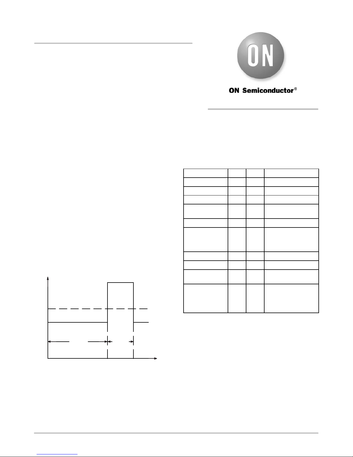
Output Current (A)
Figure 1. Transient Output Current Specification
700 ms
time (ms)
300 ms
The system has a low voltage standby mode enabled by
pulling the MC node low. In standby mode the converter
supplies 70 mA of standby current at 7.25 V while
maintaining input power below 1 W. The system is
self−contained, with the NCP1219 bias being provided by
the bulk voltage through an internal startup circuit. The IC
© Semiconductor Components Industries, LLC, 2012
November, 2012 − Rev. 3
0.92 A
Design Procedure
The converter design procedure is divided into several
steps:
• Power Component Selection
• Loop Stability Analysis and Compensation
• IC Supply Circuits
• External Protection Circuits
• Standby Reconfiguration Circuit
Throughout this application note, the minimum and
maximum input voltages are referred as low and high line,
respectively.
The evaluation board schematic is provided in Figure 2
for reference to component values throughout the design
procedure.
1 Publication Order Number:
EVBUM2161/D
Page 2
J5
123
C20
220uF/6.3V
SGND
NCP1219PRINTGEVB
R34
R35
10K
1k
R32
U4
TL431B
2.26K
Q6
2N7002L
R33
8.06k
330mF/35V
C16
L1
2.2u
1000uF/35V
C15
C14
470pF/250V
D12
100
R18
JP1
1N4007
D2
1N4007
D1
T1
4.75M
R1
F1
C1
2A/250V
C10
C6
JP3
10u, 1.4A
4.75M
R2
0.22mF/275V
MUR420RLG
5
T2
D10
4700pF/630V
R14
120K/0.5W
100u/400V
D13
D4
1N4007
D3
431
1N4007
6
1N4007RLG
1N4007
R15
D6
VCC
2
10
MMSD914T1G
C7
open
000
R13
JP2
1
HS1
Q5
R5
1.4M
VHOUT
2
C21
20
R9
R20
SPA07N65C3
R37
10K
22u/25V
1.82K
R41
open
R11
R8
1.4M
open
open
R10
R16
ZD1
open
12
4
U2
open
R51
1.69
R52
1.69
R53
1.69
R54
1.69
1.82K
R42
LATCH
open
ZD2
3
U1
open
LATCH
HV
Skip/
latch
C18
open
R30
Q3
1nF/440V
D5
J4
VCC
CS
C5
open
open
open
VHOUT
MMSD914T1G
ZD4
open
C3
0.1/25V
DRV
GND
NCP1219AD65R2G
100p
R12
open
C8
open
990
R23
J3
J2
R4
JP4
C9
R6
10
FB
C4
C2
1000p
R3
open
VHOUT
R24
2.49K
12
4
412
U3
SFH615A-3
R31
R25
3
19.6K
C19
0
0.033
J1
AC Connector C8
Figure 2. Evaluation Board Schematic
http://onsemi.com
2
Page 3

NCP1219PRINTGEVB
Transformer
The turns ratio, N, is chosen to minimize the voltage
stresses placed on main switch, Q5, and the secondary diode,
D12. N is calculated using Equation 1,
) V
Ǔ
f
bulk(max)
(eq. 1)
N +
@ǒV
BV
DSS
k
out
C
@ kD* VOS* V
N
S
+
N
P
where NS is the number of turns on the secondary winding,
N
is the number of turns on the primary winding, kc is the
P
clamp voltage ratio, V
is the regulated output voltage, V
out
is the forward voltage drop of the secondary rectifying
diode, BV
k
is the derating factor of the main switch, Vos is the clamp
D
voltage overshoot, and V
where f
I
out(crit)
is the breakdown voltage of the main switch,
DSS
bulk(max)
L
P(crit)
is the switching frequency of the controller, and
osc
is the maximum DC bulk
+
2 @ f
OSC
@ V
out
@ I
out(crit)
h @ V
@ǒV
is the load current at which the transition between
DCM and CCM occurs. By operating in the transition
between DCM and CCM, the secondary RMS current is
minimized, reducing the requirements on the transformer
and output capacitor. For the evaluation board design, with
a transition occurring at I
= 1.6 A, the primary inductance
out
is 350 mH.
Sense Resistor
To calculate the value of the current current sense resistor,
R
, the peak current of the primary winding of the
sense
transformer must first be calculated. The energy storage
relationship is used to determine the peak primary current,
calculated using Equation 3.
I
peak
+
Ǹ
L
P(crit)
@ f
out
OSC
@ h
(eq. 3)
2 @ P
Using the specified peak output power to calculate the
peak primary current:
Ǹ
2 @ 48 W
350 mH @ 65 kHz @ 85%
+ 2.23 A
The NCP1219 has a current limit comparator reference
voltage, V
, of 1 V, typical. R
ILIM
, is calculated using
sense
Equation 4.
V
+
PWM
I
peak
R
sense
This results in a value of 449 mW for R
(eq. 4)
sense
(R51||R52||R53||R54). A 430 mW resistor is chosen for
sufficient margin to deliver the peak output power.
voltage supplying the controller. Using a 650 V MOSFET
with a derating factor of 0.8 and a clamp voltage ratio, k
1.6 yields a turns ratio of 0.303. This maintains sufficient
margin for the voltage rating of the MOSFET.
The power components for the flyback topology can be
selected for operation in either discontinuous conduction
mode (DCM) or continuous conduction mode (CCM).
Measuring the tradeoffs of the two modes at the power level
required for this design, the transformer is designed to make
a transition between DCM and CCM at low line and a load
f
current of 1.6 A. This ensures that the converter operates in
DCM at nominal load. The critical primary inductance,
L
, to cause this transition is calculated using
P(crit)
Equation 2.
V
)V
out
bulk(min)
bulk(min)
2
ǒ
@
V
out
)
The primary rms current, I
f
Ǔ
N
)V
N
f
Ǔ@ǒ
V
)V
out
N
f
) h @ V
Ǔ
bulk(min)
is needed in order to
L(rms)
calculate the power dissipation in the R
maximum duty ratio, D
D
max
, is calculated using Equation 5.
max
V
+
V
out
out
) N @ V
bulk(min)
The maximum duty ratio determines the change in
primary current, ΔI
Finally, ΔIL is used to calculate I
I
+ D
L(RMS)
, as shown in Equation 6.
L
V
max
bulk(min)
L
pri
@ǒI
peak
@ f
DIL+
Ǹ
@ D
OSC
2
* I
max
as in Equation 7.
L(RMS)
@ DIL)
peak
The power dissipated in the sense resistor is then calculated
using Equation 8.
P
R
sense
+ I
L(RMS)
2
@ R
sense
The power rating of the resistor is chosen to handle the
maximum power dissipation. For this design, the worst case
peak power dissipation is calculated to be 400 mW. Four
1206 surface mount resistors in parallel are chosen to
dissipate the power. Note that this is the worst case power
dissipation calculated assuming a continuous output current
of 2 A. For normal operating conditions (I
out
power dissipation is 208 mW.
(eq. 2)
. First, the
sense
(eq. 5)
(eq. 6)
(eq. 7)
2
DI
L
Ǔ
2
(eq. 8)
= 1.25 A), the
c
, of
http://onsemi.com
3
Page 4

NCP1219PRINTGEVB
Primary Switch
The main MOSFET switch, Q5, is selected to operate at
a junction temperature of 120°C at an ambient temperature
of 85°C. The maximum power dissipation for Q5 is
calculated using Equation 9, where T
junction temperature, T
is the thermal resistance of the MOSFET.
R
JA
q
An isolated TO−220 with an R
is the ambient temperature, and
A
ǒ
T
* T
+
max
R
qJA
JA
q
P
max
maximum power dissipation of 438 mW. The R
is the maximum
MAX
Ǔ
A
(eq. 9)
of 80°C/W results in a
DS(on)
required to satisfy the maximum power dissipation at
nominal load is approximated by Equation 10. The value is
taken from the datasheet curves for the desired junction
temperature, provided by the MOSFET manufacturer.
P
R
DS(on)
+
I
L(RMS)
max
2
(eq. 10)
The MOSFET is sized so that the thermal requirements
are met under nominal load (30 W). Equation 3 is used to
determine the peak current, in this case using 30 W for P
out
yielding a peak current of 1.7 A.
The controller operates in DCM at low−line and nominal
load. The equation for the primary rms current in DCM is
shown in Equation 11. In this example, the primary rms
current is calculated to be 0.69 A.
D
max
I
L(RMS)
+ I
peak
Ǹ
@
3
(eq. 11)
Substituting the resulting primary rms current into
Equation 10, we find an R
of less than 1.1 W is
DS(on)
required. The Infineon SPA07N65C3 n−channel MOSFET,
with R
conservative approach to the selection of Q5. The R
= 600 mW is used in this design. This is a
DS(on)
used
JA
q
to calculate the maximum power dissipation assumes the
MOSFET operates in free air, without a heat sink. This
design includes an aluminum heat sink attached to the body
of the TO−220, reducing the thermal resistance and
increasing the maximum power capability of the MOSFET.
Secondary Rectifier
The peak inverse voltage, PIV, of D12 is calculated by
Equation 12.
PIV + V
375 V @ 0.303 ) 24 V + 138 V
bulk(max)
@ N ) V
out
(eq. 12)
Applying a silicon derating factor of 0.8 to PIV, the
minimum breakdown voltage of D12 must be greater than
173 V. An MUR420, 200 V ultrafast rectifier is selected.
The power dissipated in the secondary diode, P
approximated by Equation 13, where V
voltage of the selected diode, and I
out
is the forward
f
is the nominal output
current of the converter.
Pd+ Vf@ I
Output Capacitor
out
The output capacitor is selected to satisfy the output
voltage ripple requirements of the controller. The output
capacitor must supply the entire output current during the
controller on time. The capacitor value is calculated using
Equation 14,
I
@ t
out
C
+
out
where t
is the maximum on time of the controller,
on(max)
which can be calculated using D
on(max)
V
ripple
from Equation 5. For
max
this design, Equation 14 results in a capacitor value of 70 mF.
The effective series resistance, ESR, of the capacitor also
plays a significant role in the selection of the output
capacitor. The secondary peak current charges the output
,
capacitor during each cycle, and the ESR must not cause a
voltage drop greater than the ripple voltage. The acceptable
ESR is calculated using Equation 15,
V
ripple
I
sec(peak)
where I
sec(peak)
ESR v
is proportional to the primary peak current
by the turns ratio, as given by Equation 16.
I
I
sec(peak)
+
pri(peak)
N
An ESR of 31 mW is required to meet the 200 mV output
ripple requirement.
The output capacitor also has a specified rms current
capability that must be considered. The rms current seen by
the capacitor, I
where I
Cout(RMS)
I
Cout(RMS)
is the maximum dc load current supplied by
out(avg)
the converter and I
, is calculated using Equation 17,
Ǹ
+ I
sec(RMS)
sec(RMS)
is the secondary rms current. For
2
* I
out(avg)
the maximum load current, the controller operated in CCM
and I
sec(RMS)
For this design at maximum load, I
is calculated using Equation 18.
Cout(RMS)
output capacitor with an ESR of 18 mW and an rms ripple
current capability of 2.77 A is selected, and the resulting
capacitor value is 1000 mF.
is
d
(eq. 13)
(eq. 14)
(eq. 15)
(eq. 16)
2
(eq. 17)
is 2.44 A. An
I
sec(RMS)
+
Ǹ
(
1 * D
)
ǒ
I
@
max
sec(peak)
http://onsemi.com
DI
L
N2@ 3
2
(eq. 18)
Ǔ
DI
2
* I
sec(peak)
4
L
@
)
N
Page 5
NCP1219PRINTGEVB
Auxiliary Supply Regulator
The HV pin of the NCP1219 can be tied directly to the
bulk storage capacitor and used to supply the IC in the
absence of an auxiliary winding, for instance, during the
startup of the adapter. The startup current is controlled
internally and supplied to the V
V
pin. While VCC is less than the Inhibit threshold
CC
voltage, the V
capacitor is charged with a current source
CC
capacitor through the
CC
of 200 mA (typical). Once the inhibit threshold is exceeded,
the startup current (typically 13.5 mA) is supplied to the
VCC capacitor. When V
current source is disabled, and the V
discharged until V
decreases to less than V
CC
is exceeded, the internal
CC(on)
capacitor is
CC
CC(MIN)
, at
which time the startup current source is enabled, starting the
DSS cycle over again.
The evaluation board contains several options for the HV
pin connection and the biasing of V
is used to supply V
at high line conditions in order to
CC
. An auxiliary winding
CC
satisfy the low standby power requirement of 1 W.
Option 1 – Bulk Connection with Forward Auxiliary
Winding
Connecting the HV pin to the bulk voltage and using a
forward auxiliary winding provides an IC bias dependant on
input voltage, but independent of the output voltage. This is
required in this design due to the dual output voltage design.
Otherwise the converter would require additional circuitry
to prevent the converter from entering DSS mode during the
standby conditions. Figure 3 shows this configuration. The
voltage is supplied by the auxiliary winding through a series
diode.
NAńNP+
ǒ
VCC) V
V
bulk
Ǔ
f
(eq. 19)
This implies that, as the input voltage drops, the auxiliary
winding can not supply the IC. When V
V
CC(MIN)
supplied to the V
, the startup circuit is enabled and the IC bias is
capacitor by the internal current source.
CC
reduces to
CC
Alternately, an auxiliary voltage greater than 20 V can be
used by clamping V
using a zener diode, minimizing the
CC
input voltage at which the controller enters DSS mode. This
is shown in Figure 4.
D12
V
out
Skip/
HV
latch
FB
CS
VCC
GND
DRV
NCP1219
Figure 4. VCC Connection using a Forward Auxilliary
Winding with Added Zener
Option 2 – Full−time DSS Mode (No Auxiliary Winding)
The auxiliary winding is not necessary with DSS mode, so
the connection to the auxiliary winding can be removed
altogether, as shown in Figure 5.
D12
V
out
Skip/
HV
latch
FB
CS
VCC
GND
DRV
NCP1219
Figure 3. VCC Connection Using a Forward Auxiliary
Winding with DSS at Low−Line
The voltage on the VCC pin can not exceed 20 V.
Therefore the ratio between the number of turns on the
auxiliary winding, NA, and the primary winding, N
chosen to maintain V
voltage. N
is calculated using Equation 19.
A/NP
below 20 V at the maximum input
CC
, is
A/NP
http://onsemi.com
D12
Skip/
HV
latch
FB
CS
VCC
GND
DRV
NCP1219
Figure 5. VCC Connection with Full−Time DSS Mode
(No Auxiliary Winding)
If standby power dissipation is not an issue, this option
eliminates the extra components used with the auxiliary
5
V
out
Page 6
NCP1219PRINTGEVB
winding. Care must be taken not to exceed the thermal
capability of the IC. The power dissipated during DSS mode
is approximated by Equation 20.
P
+ I
DSS
where VHV is the HV pin voltage, and I
CC3
@ V
HV
is the controller
CC3
supply current during normal switching operation. I
(eq. 20)
has
CC3
a component that is dependant on the gate charge of Q5, as
shown in Equation 21,
(eq. 21)
where Q
I
+ I
CC3
is the total gate charge of Q5.
g(tot)
CC2
) Q
g(tot)
@ f
SW
The amount of power the controller is capable of
dissipating depends on many factors, including the V
CC
capacitor value, airflow conditions, proximity of the
controller to other heat generating components on the board,
and the layout of the metal traces on the board and their heat
spreading characteristics. To determine the thermal
characteristics of the controller in the application, the
evaluation board is placed in a controlled ambient
temperature and the V
shutdown is measured. R
that results in temperature
HV
of the controller is given by
JA
q
Eequation 22,
T
* T
DSS
A
(eq. 22)
+
SHDN
P
R
qJA
where TA is the ambient temperature of the system and
T
is the junction temperature at which a thermal
SHDN
shutdown (TSD) fault occurs. For the evaluation board, with
the HV pin tied directly to V
a TSD event, and R
is calculated as 82.5°C/W.
JA
q
It is common to include a resistor, R
, a VHV of 257 V results in
bulk
, in series between
bulk
the bulk voltage and the HV pin to spread the power
dissipation between the controller and R
bulk
. R
bulk
often
consists of at least two resistors in series for protection
against shorted component testing. The same power
dissipation limit is imposed on the controller as in the case
where no series resistor is used. Therefore, adding R
bulk
allows the maximum bulk voltage to increase by dissipating
the difference in the power while the startup circuit is
charging C
. The increased bulk voltage is given by
CC
Equation 23,
P
+
I
DSS
CC3
) I
start
@ R
bulk
(eq. 23)
where P
the R
q
V
bulk
is found by rearranging Equation 22 and using
DSS
measured above.
JA
When adding the series resistors, it is recommended to
maintain a minimum V
headroom to allow the startup circuit to supply I
V
pin. Therefore, at low line, the resistance between the
CC
of 40 V to ensure there is enough
HV
start
to the
bulk voltage and the HV pin can not exceed that given by
Equation 24,
ǒ
V
R
bulk
bulk(min)
v
I
start(min)
* 40 V
Ǔ
(eq. 24)
where I
start(min)
provided to the V
V
bulk(min)
more than 10 kW. For the evaluation board, R
as 3.6 kW so that I
range. For this evaluation board, with R
is the specified minimum startup current
CC
pin. I
start(min)
= 5 mA and assuming
= 90 V, the added series resistance should be no
is chosen
bulk
is 14.7 mA across the input voltage
start
= 3.6 kW, I
bulk
start
= 14.7 mA and a maximum ambient temperature of 85°C,
the resulting maximum V
is 310 V, a 53 V increase in
bulk
comparison to the limit when connecting directly to the bulk
voltage.
The power dissipated by R
during the DSS cycle is
bulk
found using the rms current supplied through the startup
circuit during the DSS cycle, given by Equation 25,
P
Rbulk
+ R
bulk
@ǒI
start(RMS)
Ǔ
(eq. 25)
2
Option 3 – Half−Wave Rectified Connection
To reduce the power dissipation of DSS mode at high
input voltage, the HV pin is connected to the half−wave
rectified node of the bridge rectifier in place of the bulk
voltage. Figure 6 illustrates this configuration.
D12
V
out
Skip/
HV
latch
FB
CS
VCC
DRV
GND
NCP1219
Figure 6. VCC Connection with Full−time DSS Mode
Supplied By the Half−Rectified Sine Wave
The average voltage applied to the HV pin is reduced
because, during half of the input voltage cycle, the HV
voltage is a function of the input sinusoid and the other half
of the cycle the input voltage is zero. The half−wave
rectified waveform is illustrated in Figure 7.
V
peak
V
AVG, (half-wave)
Half-Wave
Rectified Voltage
Figure 7. Half−Wave Rectified Waveform
time
http://onsemi.com
6
Page 7
NCP1219PRINTGEVB
The average HV pin voltage, V
AVG(half−wave)
, is
calculated using Equation 26.
V
V
AVG(half*wave)
+
Peak
p
(eq. 26)
In comparison, using the example from option 2
(full−time DSS mode with the HV pin connected to V
power dissipation, P
, of 270 mW, and a junction
DSS
bullk
temperature of 107°C is achieved.
The techniques mentioned above can be explored in
different combinations to optimize standby power and
thermal performance of the NCP1219.
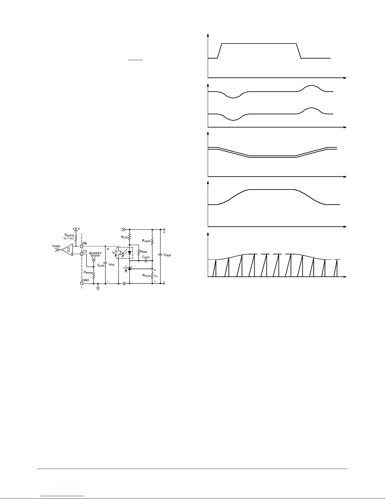
Feedback Network
The negative feedback loop that controls the output
voltage senses the output voltage using a voltage divider and
compares it to the internal reference voltage of a TL431
precision reference. The output current of the TL431 is then
a function of the bias that is required to force the internal
reference of the TL431 and the output voltage to be equal.
The TL431 output drives the cathode of an optocoupler,
providing isolation between the primary and secondary side
of the converter. The collector of the optocoupler is
connected to the FB pin of the NCP1219, closing the
feedback loop, as shown in Figure 8.
out
I
),
1
,V
out
V
2
,I
1
I
FB
V
Figure 8. Feedback Network
VFB is compared to VCS to determine the on time. If there
is an increase in load current, V
V
. This causes I1 to decrease. The optocoupler collector
out
current, I
, also decreases causing VFB to increase,
2
begins to decrease with
1
increasing on time for the next switching cycle. The timing
diagram describing the feedback loop is shown in Figure 9.
L,pri
I
time
Figure 9. Feedback Loop Timing Diagram
Standby Reconfiguration Control
The evaluation board has a dual output voltage mode. In
normal operation, the converter provides a 24 V regulated
output. During standby mode, the output supplies 7.25 V
with a standby current of 70 mA. The output voltage level
is selected by actively altering the voltage divider supplying
the feedback loop. An additional resistor is connected in
series with R32. A small signal MOSFET (Q6) is placed in
parallel with the added resistance, as shown in Figure 10.
http://onsemi.com
7
Page 8
NCP1219PRINTGEVB
Figure 10. Standby Mode Reconfiguration Circuit
When 5 V is applied to the MC pin, Q6 turns on and R33
is bypassed. In this mode, the voltage divider is set by R31
and R32 only, providing 24 V to the output. If the MC pin is
grounded or floating Q6 is off connecting R33 in series with
R32. This reduces the voltage divider value and sets the
output to 7.25 V.
Loop Stability
The output voltage regulation is provided by the negative
feedback loop described in the previous section. If the
feedback loop is not stable, the converter oscillates. To
ensure the stability of the converter, the closed loop
frequency response phase margin should be greater than 45°
at the crossover frequency. The first step in stabilizing the
closed control loop is to analyze the frequency response of
the power stage. Its contribution will determine the pole and
zero placement. The gain and pole and zero placement of the
feedback network are selected to achieve the desired
crossover frequency and phase margin.
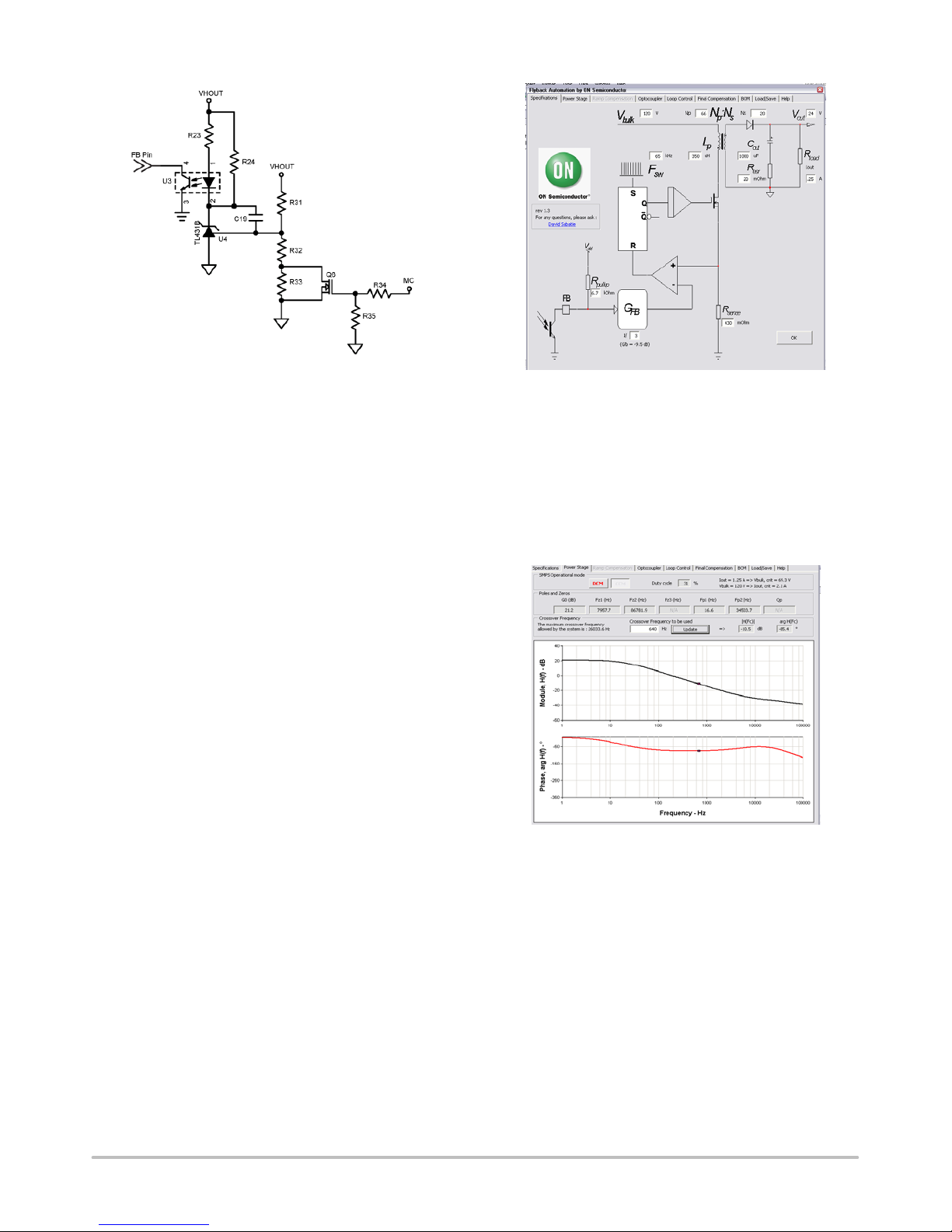
ON Semiconductor provides the excel based design tool
”FLYBACK AUTO”. It provides an automated method of
compensating the feedback loop of an isolated flyback
converter using the TL431 and an optocoupler. The tool
takes system level inputs from the user, such as bulk input
voltage, output voltage, output current, and controller
switching frequency. A screenshot of the parameter capture
screen is shown in Figure 11.
Figure 11. Screenshot of the Parameter Capture
Screen from the Design Tool FLYBACK AUTO
After the input and output parameters are entered, the
frequency response of the power stage is calculated. The
response is presented both numerically, showing the
frequency of each pole and zero, along with the dc gain of
the power stage and graphically through the use of a Bode
plot. This is shown in the screenshot presented in Figure 12.
Figure 12. Screenshot of the Power Stage Frequency
Response from the FLYBACK AUTO tool
Next, the contribution of the optocoupler to the frequency
response of the system is considered. The pole of the
compensation is selected to be less than that of the
optocoupler. The user enters information about the
optocoupler collected from the datasheet or through
frequency response characterization of the chosen
optocoupler. The optocoupler chosen for the evaluation
board design is a Vishay SFH615A−3. Using the test setup
shown in Figure 13, the optocoupler frequency response and
CTR are measured. For the frequency response
measurement, the dc bias of the 2.49 kW resistor is adjusted
until the collector of the optocoupler measured 2.5 V.
http://onsemi.com
8
Page 9
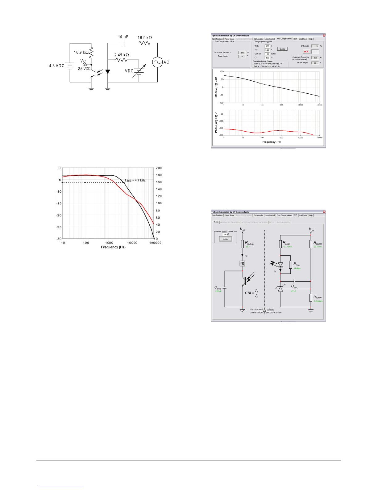
NCP1219PRINTGEVB
Figure 13. Optocoupler Frequency Analysis Test
Circuit
From Figure 14, the crossover frequency of the
SFH615A−3 is measured at 4.7 kHz. From the dc bias of the
optocoupler, the current transfer ratio, CTR is measured as
41%. These values are used in the optocoupler page of the
compensation tool.
MAG (dB)
PHASE (°)
Figure 15. Screenshot of the Total Frequency
Response Given By the Design Tool FLYBACK AUTO
A bill of materials for the compensation network is
provided by the tool based on the calculations of the
compensation network, as shown in Figure 16.
Figure 14. Frequency Response of Vishay’s
SFH615A3 Optocoupler
This data is entered into the tool and the capacitance
contribution of the optocoupler is calculated.
The pole and zero placement of the type 2 compensation
configuration is provided by the design tool based on the
desired crossover frequency and phase margin entered by
the user. If the desired crossover frequency causes the pole
frequency of the compensation network to exceed the pole
frequency of the optocoupler, then the crossover frequency
is automatically reduced.
The total loop response is provided by the design tool
based on the power stage response, optocoupler pole
location, and the type 2 compensation design. The user can
check the frequency response at various input voltages and
load conditions to verify system stability over all conditions,
as shown in Figure 15.
Figure 16. Screenshot of the Final Feedback Network
Bill of Materials
The design tool provides a good starting point; a solution
that allows the user to quickly set up a stable feedback
network. It does not, however, release the designer from
measuring the frequency response of the system and
optimizing the loop stability and transient response
tradeoffs. Using an AP Instruments AP200 frequency
response analyzer, the frequency response of the power
stage is confirmed, as shown in Figure 17. The measured
gain boost required for a crossover frequency of 1 kHz is
17 dB, slightly higher than estimated by the compensation
tool.
http://onsemi.com
9
Page 10

NCP1219PRINTGEVB
4 0
3 0
2 0
1 0
0
-1 0
Mag (dB)
-2 0
-3 0
-4 0
-5 0
-6 0
Mag (dB)
Phase (°)
1 1 0 1 0 0 1 0 0 0 1 0 0 0 0 1 0 0 0 0 0
Frequency (Hz)
Figure 17. Frequency Response of the Power Stage
The pole introduced by the optocoupler needs to be
considered. The pole location is dependant on the biasing
conditions of the optocoupler. The internal 16.7 kW pullup
resistor and the output capacitance of the optocoupler set the
pole at 4.7 kHz, as shown in Figure 14. The location of this
pole limits the available bandwidth of the system.
The evaluation board design uses the k−factor approach to
pole and zero placement, and a phase margin of 65° is
chosen. For the type 2 compensation network, the k−factor
is found using Equation 27,
k + tan
ǒ
2
) 45
Ǔ
(eq. 27)
PM * PS * 90
where PM is the desired phase margin, and PS is the phase
brought by the power stage. For a crossover frequency, f
c
, of
1 kHz, the phase caused by the power stage is −88°. The
resulting k value is 4.2. The pole frequency, f
, is calculated
p
using Equation 28.
fp+ fC@ k
(eq. 28)
The pole frequency for this design is equal to 4.2 kHz. The
zero frequency, f
, is calculated using Equation 29,
z
f
C
fz+
k
(eq. 29)
The zero frequency is set to 240 Hz.
The bandwidth of the optocoupler can be used to set the
pole location of the compensation network. In this case,
adding capacitance to satisfy the k−factor calculations limits
the bandwidth of the system and causes slowing of the
transient response and increased output ripple. The
capacitance needed to place the zero is calculated using
Equation 30.
C
+
zero
2 @ p @ fz@ R
For this design, a value of 33 nF is chosen for C
1
upper
zero
(eq. 30)
.
1 0 0
6 0
2 0
-2 0
-6 0
−17 dB
The required gain boost (G
-1 0 0
-1 4 0
-1 8 0
-2 2 0
-2 6 0
-3 0 0
PHASE (°)
) needed to compensate the
fc
system and provide a crossover frequency of 1 kHz is
measured as 17 dB. The gain provided by the compensation
network is calculated using Equation 31.
G
The R
fC
G + 10
value needed to produce this gain is calculated
LED
20
(eq. 31)
using Equation 32.
R
@ CTR
+
pullup
G
R
LED
From the measurements and the resulting gain, R
(eq. 32)
LED
is
990 W.
The open loop response is measured by injecting an ac
signal across R19 using a network analyzer and an isolation
transformer as shown in Figure 18. The open loop response
is the ratio of B to A.
Figure 18. Open Loop Frequency Response
Measurement Setup
The resulting loop response after compensation is shown
in Figure 19, where the crossover frequency is 1.3 kHz, with
a phase margin of 60°, measured at low−line and nominal
load current.
http://onsemi.com
10
Page 11

NCP1219PRINTGEVB
Figure 19 compares the measured results to the frequency
response produced by the “FLYBACK AUTO” tool. There
is good agreement for frequencies at or below the crossover
frequency. There is divergence at higher frequencies due to
the double pole of the output filter on the evaluation board.
The frequency of the double pole (f
) is given by
dp
Equation 33.
70
60
50
40
30
20
Mag (dB)
10
0
−10
−20
−30
10 100 1000 10000 100000
Figure 19. Total Loop Response Measured at Low Line and Nominal Load Current
Mag (dB)
SimMag (dB)
Phase (deg)
Sim Phase (deg)
FREQUENCY (Hz)
fdp+
2 @ p @ L1 @ C16
1
Ǹ
where L1 is the output inductor and C16 is the output filter
capacitor, which results in a pole frequency of 7.2 kHz. The
“FLYBACK AUTO” tool does not include an output filter
in the compensation design.
200
160
120
PM = 60°
fC = 1.3 kHz
80
40
0
−40
−80
−120
−160
−200
PHASE (°)
(eq. 33)
Skip Mode for Reduced Standby Power Dissipation
The NCP1219 employs an adjustable skip level that
reduces input power in light load and standby conditions.
V
is compared to V
FB
V
Skip/latch
causes V
, the drive pulses stop until the feedback loop
FB
Skip/latch
to increase to greater than V
. If VFB decreases to less than
Skip/latch
. V
Skip/latch
2 V
R
upper
42.0 k
R
lower
51.3 k
V
Skip/latch
+
-
Skip/latch
R
skip
C
skip
FB
Figure 20. Adjustable Skip Level Circuit Configuration
is adjustable by connecting an external resistor between the
Skip/latch and GND pins, as shown in Figure 20. If no
resistor is connected between the pins, the skip threshold is
the default value, V
. If the voltage on the Skip/latch pin
skip
exceeds 1.3 V, then the skip threshold is clamped to
V
skip(MAX)
V
latch
+
-
V
Skip
, typically 1.3 V.
when VCC< V
50 us
filter
V
Skip(MAX)
V
Skip/Latch
Skip
latch-off, reset
CC(reset)
S
R Q
+
-
Comparator
To DRV
latch
reset
http://onsemi.com
11
Page 12

NCP1219PRINTGEVB
Under light load conditions, the controller enters skip
mode. As seen in Figure 21, when V
than V
Skip/latch
causes V
Figure 21. Skip Mode Operation Waveforms; C1 =
(C1) the drive pulses stop (C4). This in turn
to increase as V
FB
V
Skip/latch
, C2 = VCC, C3 = VFB, C4 = V
out
Peak Primary Current
(C3) decreases to less
FB
decreases.
DRV
For the evaluation board design, the NCP1219 default
skip threshold is used to reduce component count. Selecting
a higher skip threshold has tradeoffs. If the skip voltage is set
too high, during normal operation at nominal loads the
system is in skip mode. This can cause audible noise. On the
other hand, when the board is operating in standby mode and
the load is very low, a higher skip threshold minimizes the
number of switching cycles per skip cycle. This reduces
standby power.
Overpower Compensation
For this evaluation board, without overpower
compensation, overcurrent protection occurs at a measured
output power of 67.2 W at high line and 57.4 W at low line
conditions. The variation in overcurrent output power with
input voltage is due to the propagation delay (t
PWM comparator. t
has an increased effect on the power
delay
delay
) of the
delivered at high line than at low line as shown in Figure 22.
Higher peak current
I
peak
230 Vac
120 Vac
0
t
delay
t
delay
Figure 22. Overpower Effect Due to Propagation Delay
Slope = V
bulk/Lp
time
http://onsemi.com
12
Page 13

NCP1219PRINTGEVB
This effect is called “Over power” because it increases the
power at which the overcurrent protection disables the
controller. Specifically, for a DCM flyback system, the total
power delivered to the output including the propagation
delay effect is:
delay
2
Ǔ
@ fSW@ h
V
1
P
+
out
@ LP@ǒI
2
peak
)
bulk
L
@ t
p
The NCP1219 is designed with a very short t
delay
(eq. 34)
(59 ns
typical). This minimizes the overpower. If a tighter
overpower limit is required, then overpower compensation
is implemented by using the circuits shown in Figures 23
and 24.
V
bulk
HV
Skip/
R
OPP
latch
FB
CS
GND
R
comp
VCC
DRV
R
sense
Figure 23. Overpower Compensation Circuit Using
the Bulk Capacitor Voltage
HV
Skip/
latch
R
FB
CS
comp
VCC
DRVGND
R
sense
Pri
Aux
R
OPP
Figure 24. Overpower Compensation Circuit Using a
Forward Auxiliary Winding
The circuit in Figure 23 modifies the I
peak
setpoint
proportional to the HV bulk level. The voltage divider
formed by R
OPP
and R
creates an offset that
comp
compensates for the propagation delay, but increases power
dissipation. Figure 24 provides another option that results in
reduced power dissipation. By altering the connection of the
auxiliary winding diode, a new setpoint is created whose
voltage is proportional to V
reduced by a factor of (N
. The power dissipation is
in
pri:Naux
)2.
To determine the required amount of compensation, first
the peak current for the overcurrent power at high line is
calculated using Equation 35.
I
peak
+
Ǹ
Lp@ f
OSC
out
@ h
(eq. 35)
2 @ P
Using the measured output power at high line, the
calculated peak current of 2.63 A causes a voltage on the
sense resistor, as in Equation 36.
V
sense(peak)
+ I
peak
@ R
sense
(eq. 36)
The resulting sense voltage is 1.13 V. Under high line
conditions, the desired overpower output current is 2.5 A
(60 W). Calculate the sense voltage associated with the
desired output power using the same method. In this case, an
output power of 60 W results in a sense voltage of 1.06 V.
The difference between the calculated sense voltages is
given by Equation 37.
V
CS(offset)
For this design V
+ V
sense(peak1)
CS(offset)
* V
sense(peak2)
(eq. 37)
is 70 mV. This represents the
offset voltage required on the CS pin to force the controller
to enter overcurrent protection at the desired output power.
If the circuit in Figure 23 is chosen, the R
resistor is
OPP
selected to ensure the power dissipation of the circuit does
not exceed the desired maximum, P
. For this design
OPP
50 mW is selected. The resistor value is calculated using
Equation 38.
2
P
OPP
, creating
comp
) on the CS pin to
(eq. 38)
R
+
OPP
R
creates a current that flows through R
OPP
the necessary offset (V
CS(offset)
V
bulk(max)
compensate for the propagation delay. The current is
calculated with Equation 39.
I
OPP
+
V
bulk(max)
V
CS(offset)
* 1V
(eq. 39)
The ramp compensation resistor also creates an offset
voltage due to the ramp compensation current supplied by
the controller. The internal current ramp has a slope of
8.12 mA/ms. The controller on time is measured near the
current limit in order to determine the peak voltage on the
ramp compensation resistor. The total effect of the added
compensation is shown in Equation 40.
V
R
+
ramp
8.12 Ańs @ ton)
R
is chosen to be 2.8 MW. R
OPP
CS(offset)
V
bulk(max)
R
OPP
is chosen to be 412 W
ramp
*1
(eq. 40)
to achieve an overcurrent limit at 60 W under high line
conditions. The low line overcurrent limit must also be
confirmed to ensure that the peak power is delivered with the
overpower compensation circuit. The low line current limit
for this design is measured to be 2.2 A (52.8 W).
http://onsemi.com
13
Page 14

NCP1219PRINTGEVB
Overvoltage Protection
Overvoltage protection (OVP) is implemented on this
evaluation board using one of two options; primary side
overvoltage protection or secondary side overvoltage
protection.
Primary side OVP is implemented as shown in Figure 25.
With the auxiliary winding in a flyback configuration, V
CC
is proportional to the output voltage. A zener diode and
series current limiting resistor are connected between the
Skip/latch pin of the controller and V
voltage starts to rise, V
rises and current starts to flow
CC
. If the output
CC
through ZD1. The zener current causes the voltage on the
Skip/latch pin to exceed the latch threshold and the
controller enters latched fault mode.
D6
R15
R11
ZD1
Skip/
latch
FB
CS
GND
HV
VCC
DRV
C7
options included on this evaluation board. For example, the
latch pin may be used to implement temperature shutdown
externally using an NTC element driving the base of a
bipolar transistor, Q1, as shown in Figure 27. The NTC
value is chosen so that the voltage divider made between it
and R
controller enters a latched fault, V
than V
turn on Q1 at the proper temperature. Once the
be
must decrease lower
CC
CC(reset)
to reset the controller. This is typically
achieved by removing power from the mains.
R
be
Q1
NTC
Skip/
HV
latch
FB
CS
VCC
GND
DRV
Figure 27. Temperature Shutdown Latch Circuit
Figure 25. Primary Overvoltage Protection Circuit
A secondary side OVP latch function is implemented
using the circuit shown in Figure 26. The primary and
secondary sides are isolated using an optocoupler. The zener
diode ZD2 starts to conduct if the output voltage exceeds the
regulated voltage. The current conducted by ZD2 biases Q3
and causes current to flow from the cathode of the
optocoupler. The optocoupler transistor turns on and the
voltage on the Skip/latch pin increases, latching the
controller. The value of R10 is chosen in order to limit the
voltage applied to the Skip/latch pin during a fault condition.
VHOUT
VCC
Skip/
latch
FB
CS
VCC
DRVGND
HV
R10
U2
R20
ZD2
Q3
R30 C18
Figure 26. Secondary Overvoltage Protection Circuit
Latch Protection
The latching fault protection offered by the NCP1219 can
also be used to implement other convenient board level
protection functions besides the overvoltage protection
Any other generic latched fault can be implemented using
a circuit similar to Figure 28. A fault signal is applied to the
base of an npn bipolar transistor, Q2, whose cathode drives
the base of a pnp bipolar transistor, Q1, bringing the
Skip/latch pin high.
Q1
Skip/
HV
Latch Off
Signal
Q2
latch
FB
CS
GND
VCC
DRV
Figure 28. Generic Latched Shutdown Example
SOFT−START
Soft−start reduces stress during power up by slowly
increasing the peak current until the soft−start timer expires.
The NCP1219 implements soft−start by comparing the CS
pin voltage to the lesser of the internal divided by three FB
voltage or the internal soft−start ramp. The soft−start
management block of the NCP1219 controller enables the
soft−start voltage ramp to rise in 4.8 ms. Figure 29 shows the
current sense waveform taken differentially across the sense
resistor, as the current ramps up during the first 4.8 ms of the
startup time.
http://onsemi.com
14
Page 15

NCP1219PRINTGEVB
Figure 29. Startup Waveforms Showing Soft−Start Behavior; C1 = V
Board Layout
The evaluation board is built using a double sided FR4
board. Through hole components are placed on the top layer
and surface mount components on the bottom layer. The
board is constructed using 2 oz copper.
During the layout process care was taken to:
1. Minimize trace length, especially for high current
loops.
2. Use wide traces for high current connections.
, C4 = VCS/20
out
3. Use a single ground connection.
4. Keep sensitive nodes away from noisy nodes such
as the drain of the power switch.
5. Place decoupling capacitors close to the pins of IC.
6. Sense output voltage at the output terminal to
improve load regulation.
Figure 30 shows the top layer of the PC board, including
the silkscreen, copper, and soldermask.
http://onsemi.com
15
Page 16

NCP1219PRINTGEVB
Figure 30. Layer 1 (Top)
Figure 31. Layer 2 (Bottom)
http://onsemi.com
16
Page 17

NCP1219PRINTGEVB
Figure 31 shows the bottom layer of the PC board,
including the silkscreen, copper, and soldermask.
The layout files may be available. Please contact your
sales representative for availability.
Design Validation
The top and bottom view of the board are shown in
Figures 32 and 33, respectively.
Figure 32. NCP1219 Evaluation Board Top View
Figure 33. NCP1219 Evaluation Board Bottom View
http://onsemi.com
17
Page 18

NCP1219PRINTGEVB
The bill of materials that accompanies the evaluation board circuit schematic of Figure 2 is listed in Table 2.
Table 2. BILL OF MATERIALS
Desig-
nator
C10 1 Capacitor,
C14 1 Capacitor,
C15 1 Capacitor,
C16 1 Capacitor,
C18 1 Capacitor,
C19 1 Capacitor,
C20 1 Capacitor,
C21 1 Capacitor,
D1, D2,
D3, D4,
D10,
D13
D5, D6 2 Switching Diode 100 V - SOD-123 ON
D12 1 Diode, Ultrafast
HS1 1 Heatsink - - Custom Ye s Ye s
Qty Description Value
C1 1 Capacitor,
C2 1 Capacitor,
C3 1 Capacitor,
C4 1 Capacitor,
C5 1 Capacitor,
C6 1 Capacitor,
C7 1 Capacitor,
C9 1 Capacitor,
F1 1 Fuse, Radial Lead 2 A, 250 V - Radial Littelfuse 3921200000 Ye s Ye s
J1 1 AC Connector IEC 320-C8 - Through
J2 1 Electrical
J3 1 Electrical
J4 1 Electrical
Metalized Poly
Film
Ceramic, SMD
Ceramic, SMD
Ceramic, SMD
Ceramic, SMD
Electrolytic
Electrolytic
Ceramic, Y-cap
Ceramic, Through
Hole
Ceramic, Through
Hole
Electrolytic
Electrolytic
Ceramic, SMD
Ceramic, SMD
Electrolytic
Electrolytic
6 Diode, Rectifier 1 A, 1000 V - Axial ON
Rectifier
Connection on Top
Layer of PCB
Connection on Top
Layer of PCB
Connection on Top
Layer of PCB
0.22 uF, 1000 V 20% Radial Kemet/
1000 pF 10% SM/0805 Vishay VJ0805Y102KXXA Ye s Yes
0.1 uF 10% SM/0805 Vishay VJ0805Y104KXXA Ye s Yes
open - SM/0805 - - Yes Ye s
100 pF 10% SM/0805 Vishay VJ0805Y101KXXA Ye s Ye s
100 uF, 400 V 20% Radial United
open - - - - Yes -
1 nF, 1000 V 20% Radial Kemet/
4700 pF, 630 V 5% Radial TDK FK20C0G2J472J Ye s Ye s
470 pF, 250 V 10% Radial TDK FK18C0G2E471J Ye s Ye s
1000 uF, 35 V 20% Radial United
330 uF, 35 V 20% Radial United
open - SM/0805 - - Yes Ye s
0.033 uF 10% SM/0805 Vishay VJ0805Y333KXJA Ye s Ye s
220 uF, 6.3 V 20% Radial United
22 uF, 25 V 20% Radial United
4 A, 200 V - Axial ON
- - - - - - -
- - - - - - -
- - - - - - -
Toler-
ance
Footprint Manufacturer
Evox-Rifa
Chemicon
Evox-Rifa
Chemicon
Chemicon
Chemicon
Chemicon
Semiconductor
Semiconductor
Semiconductor
Hole
Qualtek 770W-X2/10 Yes Ye s
Manufacturer Part
Number
PHE840MX6220MB06 Yes Ye s
EKXG401ELL820MM25S Ye s Ye s
ERO610RJ4100M Ye s Ye s
EKZE350ELL102MK25S Ye s Ye s
EKZE350ELL331MJ16S Ye s Ye s
ESMG6R3ELL221ME11D Ye s Ye s
ESMG250ELL220ME11D Yes Ye s
1N4007RLG No Yes
MMSD914T1G No Ye s
MUR420RLG No Ye s
Substi-
tution
Allowed
Lead
Free
http://onsemi.com
18
Page 19

NCP1219PRINTGEVB
Table 2. BILL OF MATERIALS
Desig-
nator
J5 1 Header, 1 Row of
JP1 1 Electrical
JP2
JP3
JP4 1 Electrical
L1 1 Inductor, Power 2.2 uH - Radial Coilcraft RFB0807-2R2L Ye s Ye s
MECHA
NICAL
MECHA
NICAL
Q3 1 Transistor, NPN
Q5 1 MOSFET, Power 7 A, 650 V - TO-220-3
Q6 1 MOSFET, Small
R1, R2 2 Resistor, SMD
R3 1 Resistor, SMD
R4 1 Resistor, SMD
R5, R8 2 Resistor, SMD
R6 1 Resistor, SMD
R9 1 Resistor, Through
R10
R11
R13 1 Resistor, Through
R14 1 Resistor, Through
R15 1 Resistor, SMD
R16 1 Resistor, Through
R18 1 Resistor, Through
R20 1 Resistor, Through
R23 1 Resistor, SMD
R24 1 Resistor, SMD
R25 1 Resistor, SMD
R30 1 Resistor, SMD open - SM/0805 - - Yes -
R31 1 Resistor, SMD
R32 1 Resistor, SMD
R33 1 Resistor, SMD
R34 1 Resistor, SMD
R35,
R37
2 jumper wire 22 AWG - - Belden 8021 Ye s Ye s
1 Screw M3 8 mm - - Building
2 Insulating tubing 22 AWG - - SPI
2 Resistor, SMD open - SM/1206 - - Yes -
2 Resistor, SMD
3
Connection on Top
Layer of PCB
Connection on Top
Layer of PCB
Bipolar
Signal
Hole
Hole
Hole
Hole
Hole
Hole
- - 0.156 Molex 26-64-4030 Ye s Ye s
- - - - - -
- - - - - - -
open - SOT-23 - - Ye s -
115 mA, 60 V - SOT-23 ON
4.75 MW
14 kW
412 W
1.4 MW
10 W
20 W
0 W
120 kW
10 W
open - Axial - - Yes -
100 W
open - Axial - - Yes -
976 W
2.49 kW
0 W
19.6 kW
2.26 kW
8.06 kW
1 kW
10 kW
Toler-
anceValueDescriptionQty
Fasteners
Technology
-31,
FullPAK
0.01 SM/1206 Vishay CRCW12064754FN Ye s Ye s
0.01 SM/0805 Vishay CRCW080520K0FN Ye s Ye s
0.01 SM/0805 Vishay CRCW08054120FN Yes Ye s
0.01 SM/1206 Vishay CRCW12061404FN Yes Ye s
0.01 SM/1206 Vishay CRCW120610R0FN Yes Ye s
0.01 Axial Yageo MFR-25FBF-20R0 Ye s Ye s
Jumper Axial Panasonic -
0.05 Axial Vishay HVR3700001203JR500 Yes Ye s
0.01 SM/1206 Vishay CRCW120610R0FN Yes Ye s
0.05 Axial Vishay 5093NW100R0JBC Yes Yes
0.01 SM/0805 Vishay CRCW08059760FN Yes Ye s
0.01 SM/1206 Vishay CRCW08052491FN Yes Ye s
0.01 SM/0805 Vishay CRCW08050000FN Yes Ye s
0.01 SM/1206 Vishay CRCW080519K6FN Ye s Ye s
0.01 SM/0805 Vishay CRCW08052K26FN Ye s Ye s
0.01 SM/0805 Vishay CRCW08058061FN Yes Ye s
0.01 SM/0805 Vishay CRCW08051K00FN Ye s Ye s
0.01 SM/0805 Vishay CRCW08051001FN Yes Ye s
Infineon SPA07N65C3 Yes Ye s
Semiconductor
ECG
Manufacturer Part
NumberManufacturerFootprint
MPMS 003 0008 PH Ye s Ye s
TTI-S22-1100-NAT Ye s Ye s
2N7002LT1G No Ye s
ERD-S2T0V Yes Ye s
Substi-
tution
Allowed
Lead
Free
http://onsemi.com
19
Page 20

NCP1219PRINTGEVB
Table 2. BILL OF MATERIALS
Desig-
nator
R41,
R42
R51,
R52,
R53,
R54
T1 1 Inductor, Common
T2 1 Transformer,
U1 1 Switchmode
U2 1 Optocoupler open - DIP-4 - - Yes -
U3 1 Optocoupler 150% CTR - DIP-4 Vishay SFH615A-3 Ye s Ye s
U4 1 Programmable
ZD1 1 Diode, Zener open - SOD-123 - - Ye s -
ZD2,
ZD4
2 Resistor, SMD
4 Resistor, SMD
Mode Choke
Flyback
Controller
Precision
Reference
2 Diode, Zener open - SOD-123 - - Yes -
1.8 kW
1.69 W
10 mH -30%,
400 uH - Custom,
NCP1219 - SOIC-7 ON
TL431B - TO-92 ON
Toler-
anceValueDescriptionQty
0.01 SM/1206 Vishay CRCW12061801FN Yes Ye s
0.01 SM/1206 Vishay CRCW12061R69FN Yes Ye s
+50%
Through
Hole
Through
Hole
Epcos B82732R2142B30 Ye s Ye s
ICE
Components
Semiconductor
Semiconductor
Manufacturer Part
NumberManufacturerFootprint
TO09002-1 Ye s Yes
NCP1219AD65R2G No Ye s
TL431BCLPRMG Ye s Ye s
1. Coilcraft components can be ordered at http://www.coilcraft.com
2. Epcos components can be ordered at http://www.epcos.com
3. ICE Components can be ordered at http://www.icecomponents.com
4. Infineon components can be ordered at http://www.infineon.com
5. Kemet components can be ordered at http://www.kemet.com
6. TDK components can be ordered at http://www.tdk.com
7. Vishay Components can be ordered at http://www.vishay.com
Substi-
tution
Allowed
Lead
Free
The converter performance is evaluated and compared to the original goals. From Table 1, the evaluation criteria includes:
1. Efficiency.
2. Standby input power.
3. Step load response.
4. Output voltage ripple.
The efficiency of the converter is measured across the
universal input voltage range. Figure 34 shows the
efficiency vs output current at 90 Vac, 100 Vac, 115 Vac,
230 Vac and 265 Vac.
100
90
80
70
60
50
40
Efficiency (%)
30
20
10
0
0% 10% 20% 30% 40% 50% 60% 70% 80% 90% 100%
Load Current (1.25 A = 100%)
90 Vac−47 Hz 100 Vac−47 Hz 115 Vac−60 Hz
230 Vac−50 Hz 265 Vac−50 Hz
Figure 34. Efficiency vs. output current
The average efficiency, h
, as defined by the Energy
avg
Star 2.0 External Power Supply (EPS) specification, was
calculated for various input voltages. The results are shown
in Figure 35. The converter is Energy Star 2.0 compliant,
maintaining h
greater than 83.5%.
avg
http://onsemi.com
20
Page 21

90
89
88
87
86
85
84
Average Efficiency (%)
83
82
81
80
50 300100 150 200 250
NCP1219PRINTGEVB
Input Voltage (Vac)
Figure 35. Average Efficiency vs. Line Voltage
The standby input power requirement is less than 1 W
over the range of input voltage. Figure 36 shows the standby
input power versus input voltage. Starting at low line, the
input power rises with increasing input voltage. At line
voltages less than 180 Vac, the controller operates in DSS
mode, because the forward auxiliary winding voltage is less
than that required to maintain V
1200
1100
1000
900
800
greater than V
CC
CC(MIN)
DSS mode
700
STANDBY POWER (mW)
600
A portion of the standby input power is due to the startup
circuit. As the input voltage increases, the auxiliary winding
begins to supply the controller and the startup circuit is no
longer active. A sudden drop in the standby input power is
observed when DSS is disabled. As the input voltage
continues to increase, so does the input power.
.
Aux winding
mode
500
80 100 120 140 160 180 280260240220200
Figure 36. Standby Power versus Input Voltage (Forward Auxiliary Winding Connection)
INPUT VOLTAGE (Vac)
http://onsemi.com
21
Page 22

NCP1219PRINTGEVB
The output voltage ripple is measured at 16 mV at high
line and full load. It is significantly less than the 50 mV
target. The output voltage ripple waveform at high line and
full load is shown in Figure 37. The ripple measured at the
switching frequency appears as expected. The output filter
eliminates the ripple associated with the switching
frequency, leaving only low amplitude spikes of noise that
are due to the switch transitions.
Figure 37. Output Voltage Ripple at High−line and Full Load
If the output ripple is observed on a longer time scale, a
component of the NCP1219 frequency jitter is observed.
The frequency jitter generated by the controller spreads the
energy generated during switching, reducing
electromagnetic interference, EMI. The bandwidth of the
system is not high enough to prevent this component. This
is shown in Figure 38. The output ripple due to the frequency
jitter is still within the target limits.
Figure 38. Frequency Jitter Component of Output Ripple at Nominal Load Current
http://onsemi.com
22
Page 23

NCP1219PRINTGEVB
The dynamic response of the converter at 24 V is
evaluated stepping the load current from 0.92 A to 2.0 A and
from 2.0 A to 0.92 A. The step load response is shown in
Figure 39. The output response to the load step is measured
as 150 mV, and recovery occurs in less than 5 ms. Response
to the transient load condition confirms the results of the
loop stability analysis.
Figure 39. Output Voltage Response to a Step Load from 0.92 A to 2.0 A
The frequency jitter component of the output waveform
previously described can be seen during the transient
response measurement.
http://onsemi.com
23
Page 24

NCP1219PRINTGEVB
Thermal Performance
This evaluation board is designed to operate with out
forced airflow as in an external printer power supply. The
thermal performance of the board is evaluated using an
infrared camera. Figures 40 through 43 show several images
of the board during a continuous load step as described in
Figure 1. Images include top and bottom layers at low and
high line. All images were taken in open air conditions
without forced airflow.
Figure 40. Thermal Image of the Top of the Board at Low Line During a Continuous Load Step Condition
Figure 41. Thermal Image of the Bottom of the Board at Low Line During a Continuous Load Step Condition
http://onsemi.com
24
Page 25

NCP1219PRINTGEVB
Figure 42. Thermal Image of the Top of the Board at High Line During a Continuous Load Step Condition
Figure 43. Thermal Image of the Bottom of the Board at High Line During a Continuous Load Step Condition
http://onsemi.com
25
Page 26

NCP1219PRINTGEVB
Most of the losses on the board are on the main switch,
transformer, secondary rectifier (D12) and secondary
snubber resistor (R18). The main switch losses are
dominated by on state conduction losses, but the aluminum
heat sink reduces the power dissipation in the device. High
peak currents during the load step create heating in the
transformer, as seen in Figures 40 and 42. The losses in D12
during load step conditions are shown in the lower
right−hand corner of the board in Figures 40 and 42. The
heat spreading from D12 can also be seen on the bottom side
of the board. The secondary snubber is designed to prevent
overvoltage stress on the secondary rectifier. The power
dissipation in R18 occurs at high line conditions when the
snubber acts to clamp the voltage on the diode, as seen in the
upper right hand corner of the board. At low line, DSS mode
is active and the power dissipation in the controller and the
series HV resistors (R41 and R42) can be seen in Figure 41.
Summary
A 30 W (48 W) converter is designed and built using the
flyback topology. The converter is implemented using the
NCP1219. The average load efficiency is measured above
83.5% over the complete operating range.
The standby input power is measured below 1 W under
universal mains operating ranges. The low standby power is
achieved using a forward auxiliary winding with DSS
operating at low line conditions only. The converter
complies with Energy Star 2.0 EPS requirements.
The converter provides excellent transient response by
minimizing overshoot, undershoot, and recovery time.
Output voltage ripple is measured at 16 mV. Phase margin
and crossover frequency are measured at 60° and 1.3 kHz,
respectively.
This evaluation board is designed to demonstrate the
features and flexibility of the NCP1219. This design is a
guideline only and does not guarantee performance for any
manufacturing or production purposes.
References
1. Basso, Christophe P. Switch−Mode Power
Supplies SPICE Simulations and Practical
Designs. 1st ed. New York, NY: MacGraw Hill.
2. Pressman, Abraham I. Switching Power Supply
Design. 1st ed. New York, NY: MacGraw Hill.
3. PWM Controller with Adjustable Skip Level and
External Latch Input Datasheet NCP1219,
www.onsemi.com.
http://onsemi.com
26
Page 27

NCP1219PRINTGEVB
TEST PROCEDURE FOR THE NCP1219PRINTGEVB EVALUATION BOARD
Required Equipment
(*Equivalent test equipment may be submitted.)
• *Chroma 61604 AC Power Source
• *Chroma 66202 Digital Power Meter
• *Agilent 34401A Multimeter
• *Chroma 6314 Electronic Load with *Chroma 63102
Module
• *Agilent E3649A DC Power Supply
Test Procedure
1. Set multimeter M1 to measure current.
2. Connect input terminal “I” of multimeter M1 to
pin 3 of connector J5.
3. Connect the input terminal “LO” of multimeter
M1 to the positive terminal of the electronic load.
4. Connect the negative terminal of the electronic
load to pin 2 of connector J5.
5. Set multimeter M2 to measure voltage.
6. Connect the input terminal “HI” of multimeter M2
to pin 3 of connector J5.
7. Connect the input terminal “LO” of multimeter
M2 to pin 2 of connector J5.
8. Connect the positive terminal of the dc power
supply to pin 1 of connector J5.
9. Connect the negative terminal of the dc power
supply to pin 2 of connector J5.
10. Connect the ac power source and power analyzer
to connector J1 as shown in Figure 44.
11. Set the current compliance limit on the ac source
to 4 A.
12. Set the ac source to 115 Vac / 60 Hz.
13. Set the electronic load to the lowest current range
setting.
14. Set the electronic load to 70 mA.
15. Set the dc power supply connected to pin1 of J5 to
0 V.
16. High voltages are present on the primary side
of the converter during testing. Use Caution.
17. Turn the dc source on.
18. Turn the ac source on.
19. Set the power analyzer to integrate power for 5
minutes and start the integration cycle.
20. Measure V
OUT(standby)
multimeter. Record the results in Table 5. Verify it
is within the limits of Table 4.
21. Measure and the integrated P
power analyzers it may be necessary to convert to
P
from W*h using the equation:
IN
using the corresponding
IN(standby)
. For some
PIN+
W h
5minutes
60minutes
1hour
+ (W h) 12
Record the results in Table 5. Verify it is within the
limits of Table 4.
22. Repeat steps 19 through 21 for a line voltage of
230 Vac / 50 Hz.
23. Set the ac power source to 115 Vac / 60 Hz.
24. Set the electronic load to 1.25 A.
25. Set the dc power supply to 5 V.
26. Perform a 5 minute burn in at the line and load
conditions given in steps 23 and 24.
27. Measure and the output voltage (V
) using the
OUT
corresponding multimeter. Record the results in
Table 6. Verify it is within the limits of Table 4.
28. Measure the output current (I
) using the
OUT
corresponding multimeter. Record the results in
Table 6.
29. Measure the input power (P
) using the power
IN
analyzer. Record the results in Table 6.
30. Calculate the efficiency (h) using the equation
I
V
h +
OUT
OUT
IN
100%
P
Record the results in Table 6.
31. Repeat steps 27 - 30 for all ac source and
electronic load settings (0.01 A, 0.3125 A,
0.625 A, 0.9375 A, 1.25 A, 2.00 A) specified in
Table 3.
32. Calculate the average efficiency (h
) using the
avg
equation:
h
avg
where h
+
25%
) h
h
25%
, h
50%
, h
50%
75%
) h
4
and h
75%
) h
100%
100%
are the
efficiencies calculated for the 25%, 50%, 75% and
100% load conditions given in Table 3.
Record the results in Table 6. Verify it is within
the limits of Table 4.
33. Turn off the ac source.
34. Turn off the dc source.
35. Disconnect the ac source.
36. Disconnect the dc source.
37. Disconnect the electronic load.
38. Disconnect both multimeters.
39. End of test.
http://onsemi.com
27
Page 28

NCP1219PRINTGEVB
Table 3. NORMAL OPERATING CONDITIONS
Input Voltage
(Vac)
115 60
230 50
Line Frequency
(Hz)
Load Current (A)
0.01
0.3125 (25%)
0.675 (50%)
0.9375 (75%)
1.25 (100%)
2.00
0.01
0.3125 (25%)
0.675 (50%)
0.9375 (75%)
1.25 (100%)
2.00
Figure 44. Test Setup
Table 4. DESIRED RESULTS
Input Voltage I
For 115 Vac /
60 Hz input
For 230 Vac /
50 Hz input
Table 5. STANDBY MODE MEASURED RESULTS
Input Voltage Parameter Result
115 Vac / 60 Hz
230 Vac / 50 Hz
Input
Input
OUT
70 mA 7 V < V
70 mA PIN < 1 W
I
specified
OUT
in Table 3
25%, 50%,
75%, 100%
V
OUT
h
avg
70 mA 7 V < V
70 mA PIN < 1 W
I
specified
OUT
in Table 3
25%, 50%,
75%, 100%
V
OUT(standby)
P
IN(standby)
V
OUT(standby)
P
IN(standby)
V
OUT
h
avg
OUT(standby)
8V
= 24 ±0.2 V
> 83.5%
OUT(standby)
8V
= 24 ±0.2 V
> 83.5%
<
<
http://onsemi.com
28
Page 29

NCP1219PRINTGEVB
Table 6. NORMAL MODE MEASURED AND
CALCULATED RESULTS
Input
Voltage
115 Vac /
60 Hz
Input
Load Cur-
rent (A)
0.01 V
0.3125
(25%)
0.675
(50%)
0.9375
(75%)
1.25
(100%)
2.00 V
Parameter Result
(V)
OUT
I
(A)
OUT
PIN (W)
V
(V)
OUT
I
(A)
OUT
PIN (W)
h
25%
V
(V)
OUT
I
(A)
OUT
PIN (W)
h
50%
V
(V)
OUT
I
(A)
OUT
PIN (W)
h
75%
V
(V)
OUT
I
(A)
OUT
PIN (W)
h
100%
(V)
OUT
I
(A)
OUT
PIN (W)
h
avg
230 Vac /
50 Hz
Input
0.01 V
0.3125
(25%)
0.675
(50%)
0.9375
(75%)
1.25
(100%)
2.00 V
OUT
I
OUT
PIN (W)
V
OUT
I
OUT
PIN (W)
h
25%
V
OUT
I
OUT
PIN (W)
h
50%
V
OUT
I
OUT
PIN (W)
h
75%
V
OUT
I
OUT
PIN (W)
h
100%
OUT
I
OUT
PIN (W)
h
avg
(V)
(A)
(V)
(A)
(V)
(A)
(V)
(A)
(V)
(A)
(V)
(A)
ON Semiconductor and are registered trademarks of Semiconductor Components Industries, LLC (SCILLC). SCILLC owns the rights to a number of patents, trademarks,
copyrights, trade secrets, and other intellectual property. A listing of SCILLC’s product/patent coverage may be accessed at www.onsemi.com/site/pdf/Patent−Marking.pdf. SCILLC
reserves the right to make changes without further notice to any products herein. SCILLC makes no warranty, representation or guarantee regarding the suitability of its products for any
particular purpose, nor does SCILLC assume any liability arising out of the application or use of any product or circuit, and specifically disclaims any and all liability, including without
limitation special, consequential or incidental damages. “Typical” parameters which may be provided in SCILLC data sheets and/or specifications can and do vary in different applications
and actual performance may vary over time. All operating parameters, including “Typicals” must be validated for each customer application by customer’s technical experts. SCILLC
does not convey any license under its patent rights nor the rights of others. SCILLC products are not designed, intended, or authorized for use as components in systems intended for
surgical implant into the body, or other applications intended to support or sustain life, or for any other application in which the failure of the SCILLC product could create a situation where
personal injury or death may occur. Should Buyer purchase or use SCILLC products for any such unintended or unauthorized application, Buyer shall indemnify and hold SCILLC and
its officers, employees, subsidiaries, affiliates, and distributors harmless against all claims, costs, damages, and expenses, and reasonable attorney fees arising out of, directly or indirectly,
any claim of personal injury or death associated with such unintended or unauthorized use, even if such claim alleges that SCILLC was negligent regarding the design or manufacture
of the part. SCILLC is an Equal Opportunity/Affirmative Action Employer. This literature is subject to all applicable copyright laws and is not for resale in any manner.
PUBLICATION ORDERING INFORMATION
LITERATURE FULFILLMENT:
Literature Distribution Center for ON Semiconductor
P.O. Box 5163, Denver, Colorado 80217 USA
Phone: 303−675−2175 or 800−344−3860 Toll Free USA/Canada
Fax: 303−675−2176 or 800−344−3867 Toll Free USA/Canada
Email: orderlit@onsemi.com
N. American Technical Support: 800−282−9855 Toll Free
USA/Canada
Europe, Middle East and Africa Technical Support:
Phone: 421 33 790 2910
Japan Customer Focus Center
Phone: 81−3−5817−1050
http://onsemi.com
29
ON Semiconductor Website: www.onsemi.com
Order Literature: http://www.onsemi.com/orderlit
For additional information, please contact your local
Sales Representative
EVBUM2161/D
 Loading...