

Page 1
查询NCP1200P60供应商
NCP1200
PWM Current−Mode
Controller for Low−Power
Universal Off−Line Supplies
Housed in SOIC−8 or PDIP−8 package, the NCP1200 represents a
major leap toward ultra−compact Switchmode Power Supplies. Due to
a novel concept, the circuit allows the implementation of a complete
offline battery charger or a standby SMPS with few external
components. Furthermore, an integrated output short−circuit
protection lets the designer build an extremely low−cost AC−DC wall
adapter associated with a simplified feedback scheme.
With an internal structure operating at a fixed 40 kHz, 60 kHz or
100 kHz, the controller drives low gate−charge switching devices like
an IGBT or a MOSFET thus requiring a very small operating power.
Due to current−mode control, the NCP1200 drastically simplifies the
design of reliable and cheap offline converters with extremely low
acoustic generation and inherent pulse−by−pulse control.
When the current setpoint falls below a given value, e.g. the output
power demand diminishes, the IC automatically enters the skip cycle
mode and provides excellent efficiency at light loads. Because this
occurs at low peak current, no acoustic noise takes place.
Finally, the IC is self−supplied from the DC rail, eliminating the
need of an auxiliary winding. This feature ensures operation in
presence of low output voltage or shorts.
Features
• No Auxiliary Winding Operation
• Internal Output Short−Circuit Protection
• Extremely Low No−Load Standby Power
• Current−Mode with Skip−Cycle Capability
• Internal Leading Edge Blanking
• 250 mA Peak Current Source/Sink Capability
• Internally Fixed Frequency at 40 kHz, 60 kHz and 100 kHz
• Direct Optocoupler Connection
• Built−in Frequency Jittering for Lower EMI
• SPICE Models Available for TRANsient and AC Analysis
• Internal Temperature Shutdown
• Pb−Free Packages are Available
http://onsemi.com
SOIC−8
8
8
1
xxx = Device Code: 40, 60 or 100
y = Device Code:
A = Assembly Location
L = Wafer Lot
Y, YY = Year
W, WW = Work Week
D SUFFIX
CASE 751
1
PDIP−8
P SUFFIX
CASE 626
4 for 40
6 for 60
1 for 100
PIN CONNECTIONS
Adj
18
FB
2
3
CS
GND
4
(Top View)
MARKING
DIAGRAMS
8
200Dy
ALYW
1
8
1200Pxxx
YYWW
1
HV
7
NC
V
6
CC
Drv
5
AWL
T ypical Applications
• AC−DC Adapters
• Offline Battery Chargers
• Auxiliary/Ancillary Power Supplies (USB, Appliances, TVs, etc.)
Semiconductor Components Industries, LLC, 2004
December, 2004 − Rev. 13
1 Publication Order Number:
ORDERING INFORMATION
See detailed ordering and shipping information in the package
dimensions section on page 14 of this data sheet.
NCP1200/D
Page 2
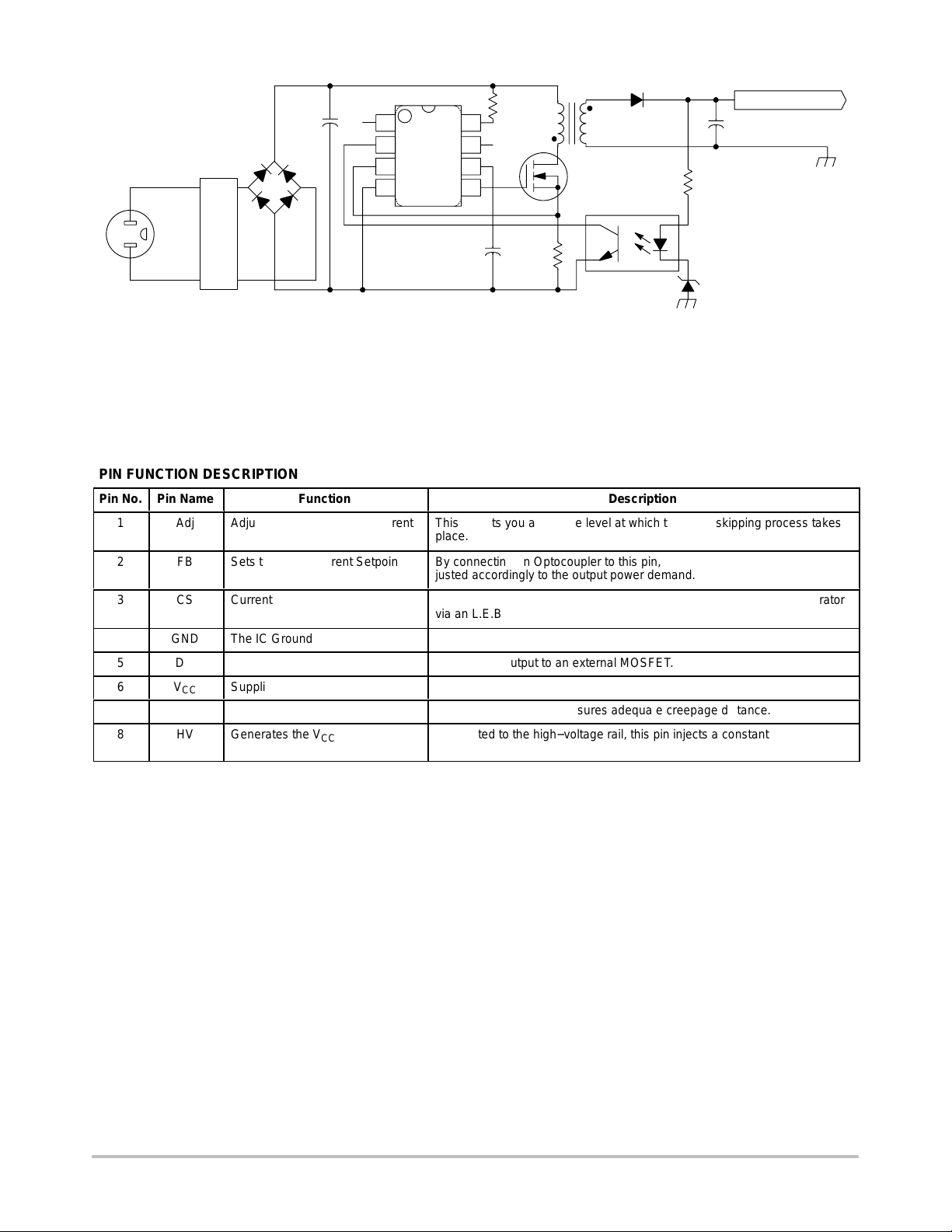
NCP1200
Á
Á
Á
Á
Á
Á
Á
Á
C3
+
10 F
400 V
EMI
Filter
Universal Input
*Please refer to the application information section
PIN FUNCTION DESCRIPTION
Pin No.
ÁÁ
ÁÁ
1
2
3
4
5
6
7
8
Pin Name
Adj
ÁÁ
FB
CS
ÁÁ
GND
Drv
V
CC
NC
HV
Function
Adjust the Skipping Peak Current
БББББББ
Sets the Peak Current Setpoint
Current Sense Input
БББББББ
The IC Ground
Driving Pulses
Supplies the IC
No Connection
Generates the VCC from the Line
*
HV
V
NC
CC
Drv
8
7
6
5
1
Adj
2
FB
3
CS
GND
4
+
C5
10 F
R
sense
Figure 1. T ypical Application
This pin lets you adjust the level at which the cycle skipping process takes
place.
БББББББББББББББББ
By connecting an Optocoupler to this pin, the peak current setpoint is adjusted accordingly to the output power demand.
This pin senses the primary current and routes it to the internal comparator
via an L.E.B.
БББББББББББББББББ
The driver’s output to an external MOSFET.
This pin is connected to an external bulk capacitor of typically 10 F.
This un−connected pin ensures adequate creepage distance.
Connected to the high−voltage rail, this pin injects a constant current into
the V
bulk capacitor.
CC
1N5819
M1
MTD1N60E
Description
D2
+
Rf
470
D8
5 V1
C2
470 F/10 V
6.5 V @ 600 mA
http://onsemi.com
2
Page 3
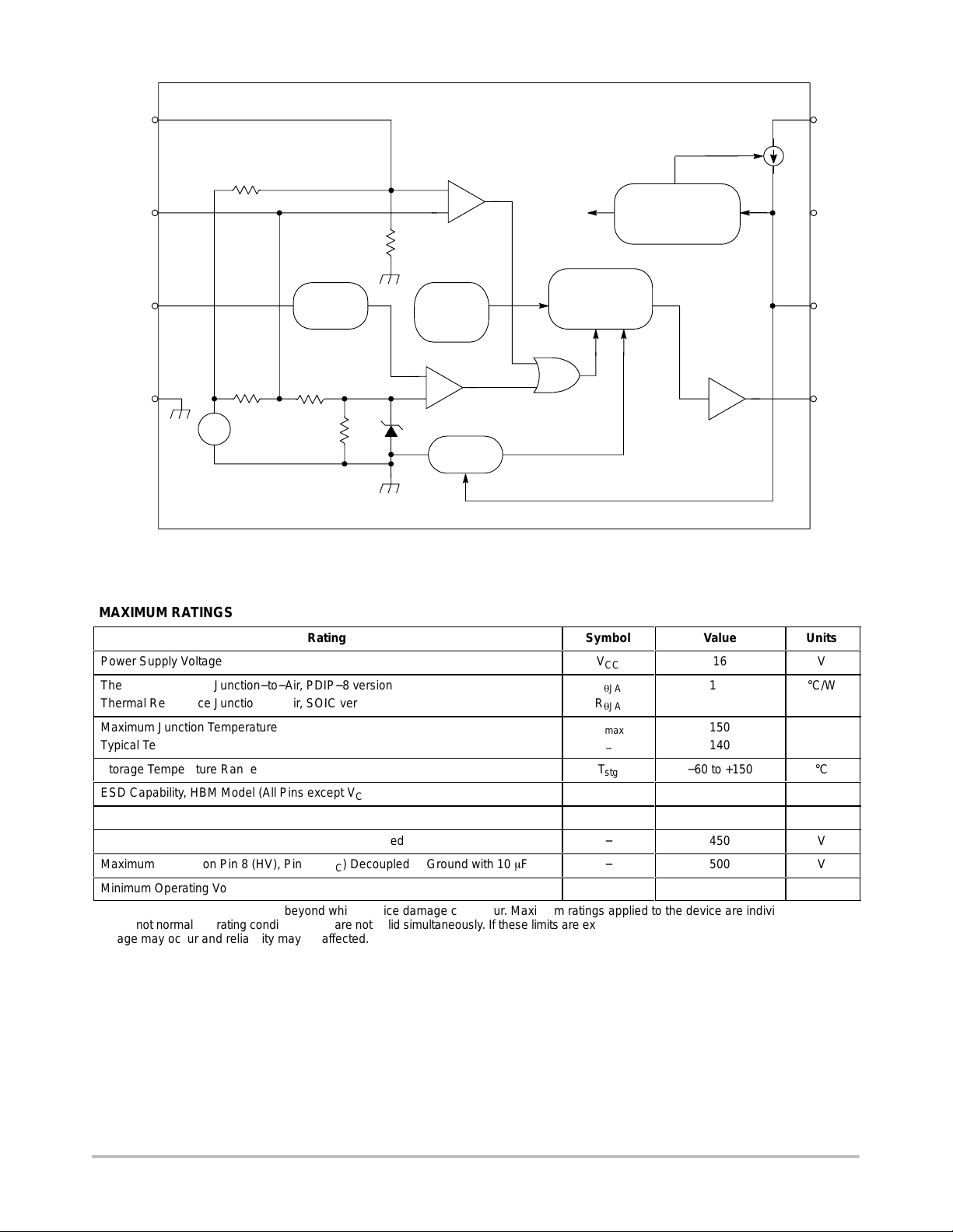
NCP1200
Á
Á
Á
Á
Adj
FB
Current
Sense
Ground
1
HV Current
8
HV
Source
75.5 k
1.4 V
2
Skip Cycle
Comparator
+
−
Internal
V
CC
UVLO
High and Low
Internal Regulator
7
NC
29 k
Q Flip−Flop
Set
3
250 ns
L.E.B.
40, 60 or
100 kHz
Clock
4
+
V
ref
−
5.2 V
60 k8 k
20 k
+
−
1 V
DCmax = 80%
Reset
Q
6
V
CC
5
Drv
±110 mA
Overload?
Fault Duration
Figure 2. Internal Circuit Architecture
MAXIMUM RATINGS
Rating
Power Supply Voltage
Thermal Resistance Junction−to−Air, PDIP−8 version
Thermal Resistance Junction−to−Air, SOIC version
БББББББББББББББББББ
Maximum Junction Temperature
Typical Temperature Shutdown
Storage Temperature Range
ESD Capability, HBM Model (All Pins except VCC and HV)
ESD Capability, Machine Model
Maximum Voltage on Pin 8 (HV), pin 6 (VCC) Grounded
Maximum Voltage on Pin 8 (HV), Pin 6 (VCC) Decoupled to Ground with 10 F
Minimum Operating Voltage on Pin 8 (HV)
Maximum ratings are those values beyond which device damage can occur. Maximum ratings applied to the device are individual stress limit
values (not normal operating conditions) and are not valid simultaneously . If these limits are exceeded, device functional operation is not implied,
damage may occur and reliability may be affected.
Symbol
V
CC
R
JA
R
JA
ÁÁÁ
T
Jmax
−
T
stg
−
−
−
−
−
Value
16
100
178
ÁÁÁÁ
150
140
−60 to +150
2.0
200
450
500
30
Units
V
°C/W
ÁÁ
°C
°C
kV
V
V
V
V
http://onsemi.com
3
Page 4
NCP1200
ELECTRICAL CHARACTERISTICS (For typical values T
V
= 11 V unless otherwise noted)
CC
Rating
= +25°C, for min/max values TJ = −25°C to +125°C, Max TJ = 150°C,
J
Pin Symbol Min Typ Max Unit
DYNAMIC SELF−SUPPLY (All Frequency Versions, Otherwise Noted)
VCC Increasing Level at Which the Current Source Turns−off 6 V
VCC Decreasing Level at Which the Current Source Turns−on 6 V
VCC Decreasing Level at Which the Latchoff Phase Ends 6 V
Internal IC Consumption, No Output Load on Pin 5 6 I
CCOFF
CCON
CClatch
CC1
10.3 11.4 12.5 V
8.8 9.8 11 V
− 6.3 − V
− 710 880
Note 1
Internal IC Consumption, 1 nF Output Load on Pin 5, FSW = 40 kHz 6 I
CC2
− 1.2 1.4
Note 2
Internal IC Consumption, 1 nF Output Load on Pin 5, FSW = 60 kHz 6 I
CC2
− 1.4 1.6
Note 2
Internal IC Consumption, 1 nF Output Load on Pin 5, FSW = 100 kHz 6 I
CC2
− 1.9 2.2
Note 2
Internal IC Consumption, Latchoff Phase 6 I
CC3
− 350 − A
INTERNAL CURRENT SOURCE
High−voltage Current Source, VCC = 10 V 8 I
High−voltage Current Source, VCC = 0 V 8 I
C1
C2
2.8 4.0 − mA
− 4.9 − mA
DRIVE OUTPUT
Output Voltage Rise−time @ CL = 1 nF, 10−90% of Output Signal
Output Voltage Fall−time @ CL = 1 nF, 10−90% of Output Signal 5 T
Source Resistance (drive = 0, Vgate = V
− 1 V) 5 R
CCHMAX
Sink Resistance (drive = 11 V, Vgate = 1 V) 5 R
5 T
OH
OL
r
f
− 67 − ns
− 28 − ns
27 40 61
5 12 25
CURRENT COMPARATOR (Pin 5 Un−loaded)
Input Bias Current @ 1 V Input Level on Pin 3 3 I
Maximum internal Current Setpoint 3 I
Default Internal Current Setpoint for Skip Cycle Operation 3 I
Propagation Delay from Current Detection to Gate OFF State 3 T
Leading Edge Blanking Duration 3 T
IB
Limit
Lskip
DEL
LEB
− 0.02 − A
0.8 0.9 1.0 V
− 350 − mV
− 100 160 ns
− 230 − ns
INTERNAL OSCILLATOR (VCC = 11 V, Pin 5 Loaded by 1 k)
Oscillation Frequency, 40 kHz Version − f
Oscillation Frequency, 60 kHz Version − f
Oscillation Frequency, 100 kHz Version − f
Built−in Frequency Jittering, FSW = 40 kHz − f
Built−in Frequency Jittering, FSW = 60 kHz − f
Built−in Frequency Jittering, FSW = 100 kHz − f
OSC
OSC
OSC
jitter
jitter
jitter
36 42 48 kHz
52 61 70 kHz
86 103 116 kHz
− 300 − Hz/V
− 450 − Hz/V
− 620 − Hz/V
Maximum Duty Cycle − Dmax 74 80 87 %
FEEDBACK SECTION (VCC = 11 V, Pin 5 Loaded by 1 k)
Internal Pullup Resistor 2 Rup − 8.0 − k
Pin 3 to Current Setpoint Division Ratio − Iratio − 4.0 − −
SKIP CYCLE GENERATION
Default skip mode level 1 Vskip 1.1 1.4 1.6 V
Pin 1 internal output impedance 1 Zout − 25 − k
1. Max value @ TJ = −25°C.
2. Max value @ T
= 25°C, please see characterization curves.
J
A
mA
mA
mA
http://onsemi.com
4
Page 5
NCP1200
60
50
40
30
20
LEAKAGE (A)
10
0
−25
9.85
9.80
9.75
9.70
(V)
9.65
CCON
V
9.60
9.55
9.50
9.45
−25 755025 100 1250
11.70
11.60
11.50
(V)
11.40
CCOFF
V
11.30
11.20
0 −25 755025 100 1250
TEMPERATURE (°C)
5025
75
100 125
11.10
Figure 3. HV Pin Leakage Current vs.
Temperature
100 kHz
60 kHz
40 kHz
TEMPERATURE (°C)
900
850
800
(A)
750
CC1
I
700
650
600
−25 755025 100 1250
100 kHz
60 kHz
40 kHz
TEMPERATURE (°C)
Figure 4. VCC OFF vs. Temperature
100 kHz
60 kHz
40 kHz
TEMPERATURE (°C)
2.10
1.90
1.70
(mA)
1.50
CC2
I
1.30
1.10
0.90
−25 755025 100 1250
Figure 5. VCC ON vs. Temperature
100 kHz
60 kHz
40 kHz
TEMPERATURE (°C)
Figure 7. I
vs. Temperature
CC2
110
104
98
92
86
80
(kHz)
74
SW
68
F
62
56
50
44
38
−25 755025 100 1250
http://onsemi.com
5
Figure 6. I
TEMPERATURE (°C)
vs. Temperature
CC1
100 kHz
60 kHz
40 kHz
Figure 8. Switching Frequency vs. T
J
Page 6
NCP1200
6.50
6.45
6.40
(V)
6.35
CCLATCHOFF
6.30
V
6.25
6.20
−25
60
50
40
30
20
10
460
430
400
370
340
(A)
310
CC3
I
280
250
220
250
TEMPERATURE (°C)
50 75 100
125
190
TEMPERATURE (°C)
Figure 9. VCC Latchoff vs. Temperature Figure 10. I
1.00
Source
Sink
0.96
0.92
0.88
0.84
CURRENT SETPOINT (V)
50 75250 100−25 125
vs. Temperature
CC3
1.34
1.33
1.32
(V)
1.31
skip
V
1.30
1.29
1.28
0
TEMPERATURE (°C)
Figure 11. DRV Source/Sink Resistances
50 75250 100−25 125
TEMPERATURE (°C)
Figure 13. V
vs. Temperature
skip
0.80
TEMPERATURE (°C)
50 75250 100−25 12550 75250 100−25 125
Figure 12. Current Sense Limit vs. Temperature
86.0
84.0
82.0
80.0
78.0
DUTY−MAX (%)
76.0
74.0
TEMPERATURE (°C)
50 75250 100−25 125
Figure 14. Max Duty Cycle vs. T emperature
http://onsemi.com
6
Page 7

NCP1200
APPLICATIONS INFORMATION
INTRODUCTION
The NCP1200 implements a standard current mode
architecture where the switch−off time is dictated by the
peak current setpoint. This component represents the ideal
candidate where low part−count is the key parameter,
particularly in low−cost AC−DC adapters, auxiliary
supplies etc. Due to its high−performance High−Voltage
technology, the NCP1200 incorporates all the necessary
components normally needed in UC384X based supplies:
timing components, feedback devices, low−pass filter and
self−supply. This later point emphasizes the fact that ON
Semiconductor’s NCP1200 does NOT need an auxiliary
winding to operate: the product is naturally supplied from
the high−voltage rail and delivers a V
to the IC. This
CC
system is called the Dynamic Self−Supply (DSS).
V
= 11.4 V
CCOFF
10.6 V Avg.
ON
Dynamic Self−Supply
The DSS principle is based on the charge/discharge of t h e
VCC bulk capacitor from a low level up to a higher level. W e
can easily describe the current source operation with a bunch
of simple logical equations:
POWER−ON: IF V
CC
< V
THEN Current Source
CCOFF
is ON, no output pulses
IF VCC decreasing > V
THEN Current Source is
CCON
OFF, output is pulsing
IF V
increasing < V
CC
THEN Current Source is
CCOFF
ON, output is pulsing
Typical values are: V
CCOFF
= 11.4 V, V
CCON
= 9.8 V
To better understand the operational principle, Figure 15’s
sketch offers the necessary light:
V
CC
V
= 9.8 V
CCON
10.00M 30.00M 50.00M 70.00M 90.00M
Figure 15. The Charge/Discharge Cycle
Over a 10 F VCC Capacitor
The DSS behavior actually depends on the internal IC
consumption and the MOSFET’s gate charge, Qg. If we
select a MOSFET like the MTD1N60E, Qg equals 11 nC
(max). W ith a maximum switching frequency of 48 kHz (for
the P40 version), the average power necessary to drive the
MOSFET (excluding the driver efficiency and neglecting
various voltage drops) is:
Fsw Qg V
cc
with
Fsw = maximum switching frequency
Qg = MOSFET’s gate charge
VCC = VGS level applied to the gate
To obtain the final driver contribution to the IC
consumption, simply divide this result by VCC: Idriver =
Fsw Qg = 530 A. The total standby power consumption
at no−load will therefore heavily rely on the internal IC
consumption plus the above driving current (altered by the
driver’s efficiency). Suppose that the IC is supplied from a
400 V DC line. To fully supply the integrated circuit, let’s
imagine the 4 mA source is ON during 8 ms and OFF during
50 ms. The IC power contribution is therefore: 400 V . 4 mA
OFF
Output Pulses
Current
Source
. 0.16 = 256 mW. If for design reasons this contribution is
still too high, several solutions exist to diminish it:
1. Use a MOSFET with lower gate charge Qg
2. Connect pin through a diode (1N4007 typically) to
one of the mains input. The average value on pin 8
2*V
becomes
mains PEAK
. Our power contribution
example drops to: 160 mW.
Dstart
1N4007
C3
4.7 F
+
400 V
EMI
Filter
Figure 16. A simple diode naturally reduces the
average voltage on pin 8
NCP1200
1
Adj
2
FB
3
CS
GND Drv
4
V
HV
NC
CC
8
7
6
5
http://onsemi.com
7
Page 8

NCP1200
3. Permanently force the VCC level above V
CCH
with
an auxiliary winding. It will automatically
disconnect the internal startup source and the IC
will be fully self−supplied from this winding.
Again, the total power drawn from the mains will
significantly decrease. Make sure the auxiliary
voltage never exceeds the 16 V limit.
Skipping Cycle Mode
The NCP1200 automatically skips switching cycles when
the output power demand drops below a given level. This is
accomplished by monitoring the FB pin. In normal
operation, pin 2 imposes a peak current accordingly to the
load value. If the load demand decreases, the internal loop
asks for less peak current. When this setpoint reaches a
determined level, the IC prevents the current from
decreasing further down and starts to blank the output
pulses: the IC enters the so−called skip cycle mode, also
named controlled burst operation. The power transfer now
depends upon the width of the pulse bunches (Figure 18 ).
Suppose we have the following component values:
Lp, primary inductance = 1 mH
F
, switching frequency = 48 kHz
SW
Ip skip = 300 mA (or 350 mV / Rsense)
The theoretical power transfer is therefore:
1
Lp Ip2 Fsw 2.2 W
2
If this IC enters skip cycle mode with a bunch length of
10 ms over a recurrent period of 100 ms, then the total power
transfer is: 2.2 . 0.1 = 220 mW.
To better understand how this skip cycle mode takes place,
a look at the operation mode versus the FB level
immediately gives the necessary insight:
When FB is above the skip cycle threshold (1.4 V by
default), the peak current cannot exceed 1 V/Rsense. When
the IC enters the skip cycle mode, the peak current cannot go
below Vpin 1 / 4 ( F i g u r e 19) . The user still has the flexibility
to alter this 1.4 V by either shunting pin 1 to ground through
a resistor or raising it through a resistor up to the desired
level.
P1
P2
P3
Figure 18. Output pulses at various power levels
(X = 5 s/div) P1<P2<P3
Max Peak
Current
Skip Cycle
Current Limit
FB
Normal Current Mode Operation
Skip Cycle Operation
Ip
= 350 mV / R
min
Figure 17. Feedback Voltage Variations
sense
4.8 V
3.8 V
Figure 19. The skip cycle takes place at low peak
currents which guarantees noise free operation
1.4 V
http://onsemi.com
8
Page 9

NCP1200
Power Dissipation
The NCP1200 is directly supplied from the DC rail
through the internal DSS circuitry. The current flowing
through the DSS is therefore the direct image of the
NCP1200 current consumption. The total power dissipation
can be evaluated using:
(V
11 V) ICC2. If we
HVDC
operate the device on a 250 VAC rail, the maximum rectified
voltage can go up to 350 VDC. As a result, the worse case
dissipation occurs on the 100 kHz version which will
dissipate 340 . 1.8 mA@Tj = −25°C = 612 mW (however
this 1.8 mA number will drop at higher operating
temperatures). Please note that in the above example, I
CC2
is based on a 1 nF capacitor loading pin 5. As seen before,
I
will depend on your MOSFET’s Qg: I
CC2
CC2
= I
CC1
+ F
sw
x Qg. Final calculations shall thus account for the total
gate−charge Q
your MOSFET will exhibit. A DIP8
g
package offers a junction−to−ambient thermal resistance
of R
100°C/W. The maximum power dissipation can
J−A
thus be computed knowing the maximum operating
ambient temperature (e.g. 70°C) together with the
maximum allowable junction temperature (125°C):
Pmax
Jmax
R
RJA
Amax
= 550 mW. As we can see, we do not
T
T
reach the worse consumption budget imposed by the 100
kHz version. Two solutions exist to cure this trouble. The
first one consists in adding some copper area around the
NCP1200 DIP8 footprint. By adding a min−pad area of 80
2
mm
of 35 copper (1 oz.) R
drops to about 75°C/W
J−A
which allows the use of the 100 kHz version. The other
solutions are:
1. Add a series diode with pin 8 (as suggested in the
above lines) to drop the maximum input voltage
down to 222 V ((2 350)/pi) and thus dissipate
less than 400 mW
2. Implement a self−supply through an auxiliary
winding to permanently disconnect the self−supply.
SOIC−8 package offers a worse R
compared to that of
J−A
the DIP8 package: 178°C/W. Again, adding some copper
area around the PCB footprint will help decrease this
number: 12 mm x 12 mm to drop R
down to 100°C/W
J−A
with 35 copper thickness (1 oz.) or 6.5 mm x 6.5 mm with
70 copper thickness (2 oz.). One can see, we do not
recommend using the SOIC package for the 100 kHz version
with DSS active as the IC may not be able to sustain the
power (except if you have the adequate place on your PCB).
However, using the solution of the series diode or the
self−supply through the auxiliary winding does not cause
any problem with this frequency version. These options are
thoroughly described in the AND8023/D.
Overload Operation
In applications where the output current is purposely not
controlled (e.g. wall adapters delivering raw DC level), it is
interesting to implement a true short−circuit protection. A
short−circuit actually forces the output voltage to be at a low
level, preventing a bias current to circulate in the
optocoupler LED. As a result, the FB pin level is pulled up
to 4.1 V, as internally imposed by the IC. The peak current
setpoint goes to the maximum and the supply delivers a
rather high power with all the associated effects. Please note
that this can also happen in case of feedback loss, e.g. a
broken optocoupler. To account for this situation, the
NCP1200 hosts a dedicated overload detection circuitry.
Once activated, this circuitry imposes to deliver pulses in a
burst manner with a low duty cycle. The system recovers
when the fault condition disappears.
During the startup phase, the peak current is pushed to the
maximum until the output voltage reaches its target and the
feedback loop takes over. This period of time depends on
normal output load conditions and the maximum peak
current allowed by the system. The time−out used by this IC
works with the V
VCC decreases from the V
decoupling capacitor: as soon as the
CC
level (typically 11.4 V) the
CCOFF
device internally watches for an overload current situation.
If this condition is still present when V
is reached, the
CCON
controller stops the driving pulses, prevents the self−supply
current source to restart and puts all the circuitry in standby ,
consuming as little as 350 A typical (I
parameter). As
CC3
a result, the VCC level slowly discharges toward 0. When
this level crosses 6.3 V typical, the controller enters a new
startup phase by turning the current source on: V
CC
rises
toward 11.4 V and again delivers output pulses at the
UVLOH crossing point. If the fault condition has been
removed before UVLOL approaches, then the IC continues
its normal operation. Otherwise, a new fault cycle takes
place. Figure 20 shows the evolution of the signals in
presence of a fault.
http://onsemi.com
9
Page 10

11.4 V
9.8 V
6.3 V
V
Drv
CC
NCP1200
Regulation
Occurs Here
Latchoff
Phase
Time
Driver
Pulses
Internal
Fault
Flag
Startup Phase
Figure 20. If the fault is relaxed during the VCC natural fall down sequence, the IC automatically resumes.
If the fault persists when VCC reached UVLOL, then the controller cuts everything off until recovery.
Calculating the VCC Capacitor
As the above section describes, the fall down sequence
depends upon the V
level: how long does it take for the
CC
VCC line to go from 11.4 V to 9.8 V? The required time
depends on the startup sequence of your system, i.e. when
you first apply the power to the IC. The corresponding
transient fault duration due to the output capacitor charging
must be less than the time needed to discharge from 11.4 V
to 9.8 V, otherwise the supply will not properly start. The test
consists in either simulating or measuring in the lab how
much time the system takes to reach the regulation at full
load. Let’s suppose that this time corresponds to 6ms.
Therefore a V
fall time of 10 ms could be well
CC
appropriated in order to not trigger the overload detection
circuitry. If the corresponding IC consumption, including
the MOSFET drive, establishes at 1.5 mA, we can calculate
the required capacitor using the following formula:
V C
t
, with V = 2V. Then for a wanted t of 10 ms,
i
C equals 8 F or 10 F for a standard value. When an
overload condition occurs, the IC blocks its internal
circuitry and its consumption drops to 350 A typical. This
appends at V
= 9.8 V and it remains stuck until V
CC
reaches 6.5 V: we are in latchoff phase. Again, using the
calculated 10 F and 350 A current consumption, this
latchoff phase lasts: 109 ms.
Fault Occurs Here
Protecting the Controller Against Negative Spikes
is the designer’s duty to avoid the presence of negative
spikes on sensitive pins. Negative signals have the bad habit
to forward bias the controller substrate and induce erratic
behaviors. Sometimes, the injection can be so strong that
internal parasitic SCRs are triggered, engendering
irremediable damages to the IC if they are a low impedance
path is offered between V
pin is often the seat of such spurious signals, the
high−voltage pin can also be the source of problems in
certain circumstances. During the turn−off sequence, e.g.
when the user unplugs the power supply, the controller is still
fed by its V
ON and OFF with a peak current limited by Rsense.
Unfortunately , if the quality coefficient Q of the resonating
network formed by Lp and Cbulk is low (e.g. the MOSFET
Rdson + Rsense are small), conditions are met to make the
circuit resonate and thus negatively bias the controller . Since
we are talking about ms pulses, the amount of injected
charge (Q = I x t) immediately latches the controller which
brutally discharges its V
CC
is of sufficient value, its stored energy damages the
controller. Figure 21 depicts a typical negative shot
occurring on the HV pin where the brutal VCC discharge
testifies for latchup.
As with any controller built upon a CMOS technology, it
Driver
Pulses
Time
Fault is
Relaxed
capacitor and keeps activating the MOSFET
CC
Time
and GND. If the current sense
CC
capacitor. If this VCC capacitor
CC
http://onsemi.com
10
Page 11

NCP1200
Figure 21. A negative spike takes place on the Bulk capacitor at the switch−off sequence
Simple and inexpensive cures exist to prevent from
internal parasitic SCR activation. One of them consists in
inserting a resistor in series with the high−voltage pin to
keep the negative current to the lowest when the bulk
becomes negative (Figure 22). Please note that the negative
spike is clamped to –2 x Vf due to the diode bridge. Please
refer to AND8069/D for power dissipation calculations.
3
Rbulk
> 4.7 k
2
+
Cbulk
1
2
3
4
8
7
6
1
5
+
CV
CC
Figure 22. A simple resistor in series avoids any
latchup in the controller
A Typical Application
Figure 24 depicts a low−cost 3.5 W AC−DC 6.5 V wall
adapter. This is a typical application where the wall−pack
must deliver a raw DC level to a given internally regulated
apparatus: toys, calculators, CD players etc. Due to the
Another option (Figure 23) consists in wiring a diode from
V
to the bulk capacitor to force VCC to reach UVLOlow
CC
sooner and thus stops the switching activity before the bulk
capacitor gets deeply discharged. For security reasons, two
diodes can be connected in series.
3
+
Cbulk
1
2
3
4
8
7
6
5
1
D3
1N4007
+
CV
CC
Figure 23. or a diode forces VCC to reach
UVLOlow sooner
inherent short−circuit protection of the NCP1200, you only
need a bunch of components around the IC, keeping the final
cost at an extremely low level. The transformer is available
from different suppliers as detailed on the following page.
http://onsemi.com
11
Page 12

NCP1200
Universal
Input
R9
10
C3
4.7 F
400 V
330 H
+
330 H
R7
L5
C2
4.7 F
400 V
L6
+
NCP1200
HV1
Adj
FB
CS
GND
V
Drv
NC
CC
C9
10 F
2
3
4
8
7
6
5
Clamping
Network
R
clamp
Clamp
D
clamp
M1
MTD1N60E
+
Figure 24. A typical AC−DC wall adapter showing the reduced part count due to the NCP1200
T1: Lp = 2.9 mH, Np:Ns = 1:0.08, leakage = 80 H, E16 core, NCP1200P40
T1
R6
2.8
D3
1N5819
Snubber
R
Snubber
C
SFH615A−2
Snubber
IC1
2.2 H
+
C5
470 F/
10 V
L4
6.5 V @ 600 mA
+
C10
4.7 F/
10 V
Optional
Networks
R2
220
D6
5 V1
To help designers during the design stage, several manufacturers propose ready−to−use transformers for the above
application, but can also develop devices based on your particular specification:
Eldor Corporation Headquarter
Via Plinio 10,
22030 Orsenigo
(Como) Italia
Tel.: +39−031−636 111
Fax : +39−031−636 280
Email: eldor@eldor.it
www.eldor.it
ref. 1: 2262.0058C: 3.5 W version
(Lp = 2.9 mH, Lleak = 80 H, E16)
ref. 2: 2262.0059A: 5 W version
(Lp = 1.6 mH, Lleak = 45 H, E16)
EGSTON GesmbH
Grafenbergerstrae 37
3730 Eggenburg
Austria
Tel.: +43 (2984) 2226−0
Fax : +43 (2984) 2226−61
Email: info@egston.com
Atelier Special de Bobinage
125 cours Jean Jaures
38130 ECHIROLLES FRANCE
Tel.: 33 (0)4 76 23 02 24
Fax: 33 (0)4 76 22 64 89
Email: asb@wanadoo.fr
ref. 1: NCP1200−10 W−UM: 10 W for USB
(Lp = 1.8 mH, 60 kHz, 1:0.1, RM8 pot core)
Coilcraft
1102 Silver Lake Road
Cary, Illinois 60013 USA
Tel: (847) 639−6400
Fax: (847) 639−1469
Email: info@coilcraft.com
http://www.coilcraft.com
ref. 1: Y8844−A: 3.5 W version
(Lp = 2.9 mH, Lleak = 65 H, E16)
ref. 2: Y8848−A: 10 W version
(Lp = 1.8 mH, Lleak = 45 H, 1:01, E core)
http://www.egston.com/english/index.htm
ref. 1: F0095001: 3.5 W version
(Lp = 2.7 mH, Lleak = 30 H, sandwich configuration, E16)
http://onsemi.com
12
Page 13

NCP1200
Improving the Output Drive Capability
The NCP1200 features an asymmetrical output stage used
to soften the EMI signature. Figure 25 depicts the way the
driver is internally made:
V
CC
Q
2
7
40
1
12
5
Q\
3
Figure 25. The higher ON resistor slows down
the MOSFET while the lower OFF resistor
ensures fast turn−off.
In some cases, it is possible to expand the output drive
capability by adding either one or two bipolar transistors.
Figures 26, 27, and 28 give solutions whether you need to
improve the turn−on time only, the turn−off time or both. Rd
is there to damp any overshoot resulting from long copper
traces. It can be omitted with short connections. Results
showed a rise fall time improvement by 5X with standard
2N2222/2N2907:
1
2
NCP1200
3
4
8
7
6
5
Rd
2N2222
2N2907
Figure 26. Improving Both Turn−On and
Turn−Off Times
1
2
NCP1200
3
4
8
7
6
5
1N4148
2N2907
Figure 27. Improving T urn−Off Time Only
1
2
NCP1200
3
4
8
7
6
5
1N4148
2N2222
To Gate
To Gate
To Gate
http://onsemi.com
13
Figure 28. Improving T urn−On Time Only
Page 14

NCP1200
If the leakage inductance is kept low, the MTD1N60E can
withstand accidental avalanche energy, e.g. during a
high−voltage spike superimposed over the mains, without
the help of a clamping network. If this leakage path
permanently forces a drain−source voltage above the
MOSFET BVdss (600 V), a clamping network is mandatory
and must be built around Rclamp and Clamp. Dclamp shall
react extremely fast and can be a MUR160 type. T o calculate
the component values, the following formulas will help you:
R
clamp =
2 V
C
clamp
clamp
(V
L
V
ripple
clamp
leak
V
Fsw R
(V
out
Ip2 Fsw
clamp
clamp
Vf sec) N)
with:
V
: the desired clamping level, must be selected to be
clamp
between 40 V to 80 V above the reflected output voltage
when the supply is heavily loaded.
V
+ Vf: the regulated output voltage level + the secondary
out
diode voltage drop
L
: the primary leakage inductance
leak
N: the Ns:Np conversion ratio
FSW: the switching frequency
V
: the clamping ripple, could be around 20 V
ripple
Another option lies in implementing a snubber network
which will damp the leakage oscillations but also provide
more capacitance at the MOSFET’s turn−off. The peak
voltage at which the leakage forces the drain is calculated
by:
L
V
max
where C
Ip
represents the total parasitic capacitance seen
lump
C
lump
leak
at the MOSFET opening. Typical values for Rsnubber and
Csnubber in this 4W application could respectively be 1.5
k and 47 pF . Further tweaking is nevertheless necessary to
tune the dissipated power versus standby power.
Available Documents
“Implementing the NCP1200 in Low−cost AC−DC
Converters”, AND8023/D.
“Conducted EMI Filter Design for the NCP1200’’,
AND8032/D.
“Ramp Compensation for the NCP1200’’, AND8029/D.
TRANSient and AC models available to download at:
http://onsemi.com/pub/NCP1200
NCP1200 design spreadsheet available to download at:
http://onsemi.com/pub/NCP1200
ORDERING INFORMATION
Device Type Marking Package Shipping
NCP1200P40 1200P40 PDIP−8 50 Units / Rail
NCP1200P40G
NCP1200D40R2
NCP1200D40R2G 200D4 SOIC−8
NCP1200P60 1200P60 PDIP−8 50 Units / Rail
NCP1200P60G
NCP1200D60R2
NCP1200D60R2G 200D6 SOIC−8
NCP1200P100 1200P100 PDIP−8 50 Units / Rail
NCP1200P100G
NCP1200D100R2
NCP1200D100R2G 200D1 SOIC−8
†For information on tape and reel specifications, including part orientation and tape sizes, please refer to our Tape and Reel Packaging
Specifications Brochure, BRD8011/D.
FSW = 40 kHz
FSW = 60 kHz
FSW = 100 kHz
1200P40 PDIP−8
(Pb−Free)
200D4 SOIC−8 2500 Units /Reel
(Pb−Free)
1200P60 PDIP−8
(Pb−Free)
200D6 SOIC−8 2500 Units /Reel
(Pb−Free)
1200P100 PDIP−8
(Pb−Free)
200D1 SOIC−8 2500 Units / Reel
(Pb−Free)
50 Units / Rail
2500 Units /Reel
50 Units / Rail
2500 Units /Reel
50 Units / Rail
2500 Units / Reel
†
http://onsemi.com
14
Page 15

NCP1200
PACKAGE DIMENSIONS
SOIC−8
D SUFFIX
CASE 751−07
ISSUE AC
−Y−
−Z−
−X−
A
58
B
1
S
0.25 (0.010)
4
M
M
Y
K
G
C
SEATING
PLANE
0.10 (0.004)
H
D
0.25 (0.010) Z
M
Y
SXS
N
X 45
M
J
NOTES:
1. DIMENSIONING AND TOLERANCING PER
ANSI Y14.5M, 1982.
2. CONTROLLING DIMENSION: MILLIMETER.
3. DIMENSION A AND B DO NOT INCLUDE
MOLD PROTRUSION.
4. MAXIMUM MOLD PROTRUSION 0.15 (0.006)
PER SIDE.
5. DIMENSION D DOES NOT INCLUDE DAMBAR
PROTRUSION. ALLOWABLE DAMBAR
PROTRUSION SHALL BE 0.127 (0.005) TOTAL
IN EXCESS OF THE D DIMENSION AT
MAXIMUM MATERIAL CONDITION.
6. 751−01 THRU 751−06 ARE OBSOLETE. NEW
STANDARD IS 751−07.
MILLIMETERS
DIMAMIN MAX MIN MAX
4.80 5.00 0.189 0.197
B 3.80 4.00 0.150 0.157
C 1.35 1.75 0.053 0.069
D 0.33 0.51 0.013 0.020
G 1.27 BSC 0.050 BSC
H 0.10 0.25 0.004 0.010
J 0.19 0.25 0.007 0.010
K 0.40 1.27 0.016 0.050
M 0 8 0 8
N 0.25 0.50 0.010 0.020
S 5.80 6.20 0.228 0.244
INCHES
SOLDERING FOOTPRINT*
1.52
0.060
7.0
0.275
0.6
0.024
4.0
0.155
1.270
0.050
SCALE 6:1
inches
mm
*For additional information on our Pb−Free strategy and soldering
details, please download the ON Semiconductor Soldering and
Mounting Techniques Reference Manual, SOLDERRM/D.
http://onsemi.com
15
Page 16

NOTE 2
−T−
SEATING
PLANE
H
58
−B−
14
F
−A−
C
N
D
G
0.13 (0.005) B
NCP1200
PACKAGE DIMENSIONS
PDIP−8
P SUFFIX
CASE 626−05
ISSUE L
NOTES:
1. DIMENSION L TO CENTER OF LEAD WHEN
FORMED PARALLEL.
2. PACKAGE CONTOUR OPTIONAL (ROUND OR
SQUARE CORNERS).
3. DIMENSIONING AND TOLERANCING PER ANSI
Y14.5M, 1982.
DIM MIN MAX MIN MAX
A 9.40 10.16 0.370 0.400
B 6.10 6.60 0.240 0.260
C 3.94 4.45 0.155 0.175
L
J
K
M
M
A
T
M
M
D 0.38 0.51 0.015 0.020
F 1.02 1.78 0.040 0.070
G 2.54 BSC 0.100 BSC
H 0.76 1.27 0.030 0.050
J 0.20 0.30 0.008 0.012
K 2.92 3.43 0.115 0.135
L 7.62 BSC 0.300 BSC
M −−− 10 −−− 10
N 0.76 1.01 0.030 0.040
INCHESMILLIMETERS
The product described herein (NCP1200), may be covered by the following U.S. patents: 6,271,735, 6,362,067, 6,385,060, 6,429,709, 6,587,357. There may
be other patents pending.
ON Semiconductor and are registered trademarks of Semiconductor Components Industries, LLC (SCILLC). SCILLC reserves the right to make changes without further notice
to any products herein. SCILLC makes no warranty, representation or guarantee regarding the suitability of its products for any particular purpose, nor does SCILLC assume any liability
arising out of the application or use of any product or circuit, and specifically disclaims any and all liability, including without limitation special, consequential or incidental damages.
“Typical” parameters which may be provided in SCILLC data sheets and/or specifications can and do vary in different applications and actual performance may vary over time. All
operating parameters, including “Typicals” must be validated for each customer application by customer’s technical experts. SCILLC does not convey any license under its patent rights
nor the rights of others. SCILLC products are not designed, intended, or authorized for use as components in systems intended for surgical implant into the body, or other applications
intended to support or sustain life, or for any other application in which the failure of the SCILLC product could create a situation where personal injury or death may occur. Should
Buyer purchase or use SCILLC products for any such unintended or unauthorized application, Buyer shall indemnify and hold SCILLC and its officers, employees, subsidiaries, affiliates,
and distributors harmless against all claims, costs, damages, and expenses, and reasonable attorney fees arising out of, directly or indirectly, any claim of personal injury or death
associated with such unintended or unauthorized use, even if such claim alleges that SCILLC was negligent regarding the design or manufacture of the part. SCILLC is an Equal
Opportunity/Affirmative Action Employer. This literature is subject to all applicable copyright laws and is not for resale in any manner.
PUBLICATION ORDERING INFORMATION
LITERATURE FULFILLMENT:
Literature Distribution Center for ON Semiconductor
P.O. Box 61312, Phoenix, Arizona 85082−1312 USA
Phone: 480−829−7710 or 800−344−3860 Toll Free USA/Canada
Fax: 480−829−7709 or 800−344−3867 Toll Free USA/Canada
Email: orderlit@onsemi.com
N. American Technical Support: 800−282−9855 Toll Free
USA/Canada
Japan: ON Semiconductor, Japan Customer Focus Center
2−9−1 Kamimeguro, Meguro−ku, Tokyo, Japan 153−0051
Phone: 81−3−5773−3850
http://onsemi.com
ON Semiconductor Website: http://onsemi.com
Order Literature: http://www.onsemi.com/litorder
For additional information, please contact your
local Sales Representative.
NCP1200/D
16
Page 17

Copyright © Each Manufacturing Company.
All Datasheets cannot be modified without permission.
This datasheet has been download from :
www.AllDataSheet.com
100% Free DataSheet Search Site.
Free Download.
No Register.
Fast Search System.
www.AllDataSheet.com
 Loading...