

查询NB2869A供应商
NCP112
Supervisory IC for Desktop
Power Supply Monitoring
The NCP112 is a highly integrated supervisory circuit that
incorporates all the functions necessary for monitoring and
controlling a multi−output switch−mode power supply system. The
NCP112 provides an ability to monitor the status of the power supply
outputs and communicate it to the system controller. The
programmable output delays protect against spurious fault
indicators.
Features
• Under and Overvoltage Protection for 3.3 V, 5.0 V and 12 V
Outputs
• Additional Adjustable Overvoltage Protection Input
• Built−in Hysteresis on all Input Pins
• Programmable Undervoltage Blanking During Power−Up
• Fault Output with 20 mA Sink Capability
• Programmable Remote On/Off Delay Time
• Programmable Power Good Delay Time
• Precision Voltage Reference with 20 mA Source Capability
• Optimized for Low−Cost 100 nF Capacitors
• Enhanced Replacement to the TSM112
T ypical Applications
• Personal Computer Switch Mode Power Supply Monitoring
• Multi−Output Power Supplies Requiring System
Supervision
http://onsemi.com
14
1
14
1
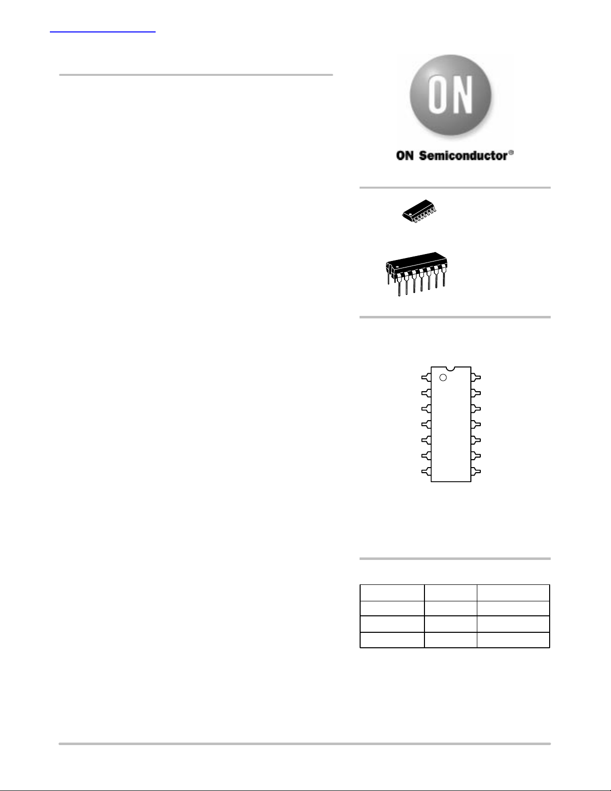
PIN CONNECTIONS AND
MARKING DIAGRAM
VS33
VS5
VS12
ADJ
PGI
CTUV
GND
AWLYYWW
NCP1 12
SOIC−14
D SUFFIX
CASE 751A
PDIP−14
P SUFFIX
CASE 646
VCC
FAULT
PGO
CTPG
CTREMOTE
REMOTE
VREF
Semiconductor Components Industries, LLC, 2004
February, 2004 − Rev. 1
PDIP−14, SOIC−14
A = Assembly Location
WL = Wafer Lot
YY = Year
WW = Work Week
ORDERING INFORMATION
Device Package Shipping†
NCP1 12P PDIP−14 25 Tube
NCP1 12D SOIC−14 55 Tube
NCP1 12DR2 SOIC−14 2500 Tape & Reel
†For information on tape and reel specifications,
including part orientation and tape sizes, please
refer to our Tape and Reel Packaging Specifications
Brochure, BRD8011/D.
1 Publication Order Number:
NCP112/D

NCP112
PIN FUNCTION DESCRIPTION
Pin No. Symbol Function Description
1 VS33 3.3 V SENSE INPUT Over/undervoltage sense input for 3.3 V .
2 VS5 5.0 V SENSE INPUT Over/undervoltage sense input for 5.0 V .
3 VS12 12 V SENSE INPUT Over/undervoltage sense input for 12 V .
4 ADJ ADJUSTABLE OVP INPUT May be used for an additional overvoltage protection signal.
5 PGI POWER GOOD INPUT Power good input signal.
6 CTUV ADJUSTABLE TIMING
CAPACITOR
7 GND GROUND Ground
8 VREF VOLTAGE REFERENCE Precision 2.5 V reference output.
9 REMOTE REMOTE ON/OFF INPUT Input remote control from the microcontroller. Acts as a reset
10 CTREMOTE ADJUSTABLE REMOTE ON/OFF
CAPACITOR
11 CTPG ADJUSTABLE POWER GOOD
CAPACITOR
12 PGO POWER GOOD OUTPUT Power good output. Active high when no fault conditions are
13 FAULT FAULT OUTPUT Detects over/undervoltage conditions. Active high during a
14 VCC POWER SUPPLY VOLTAGE Power supply voltage.
Adjustable undervoltage blanking delay during power−up.
signal after a fault condition.
Adjustable remote delay.
Adjustable power good delay.
present.
fault condition.
http://onsemi.com
2
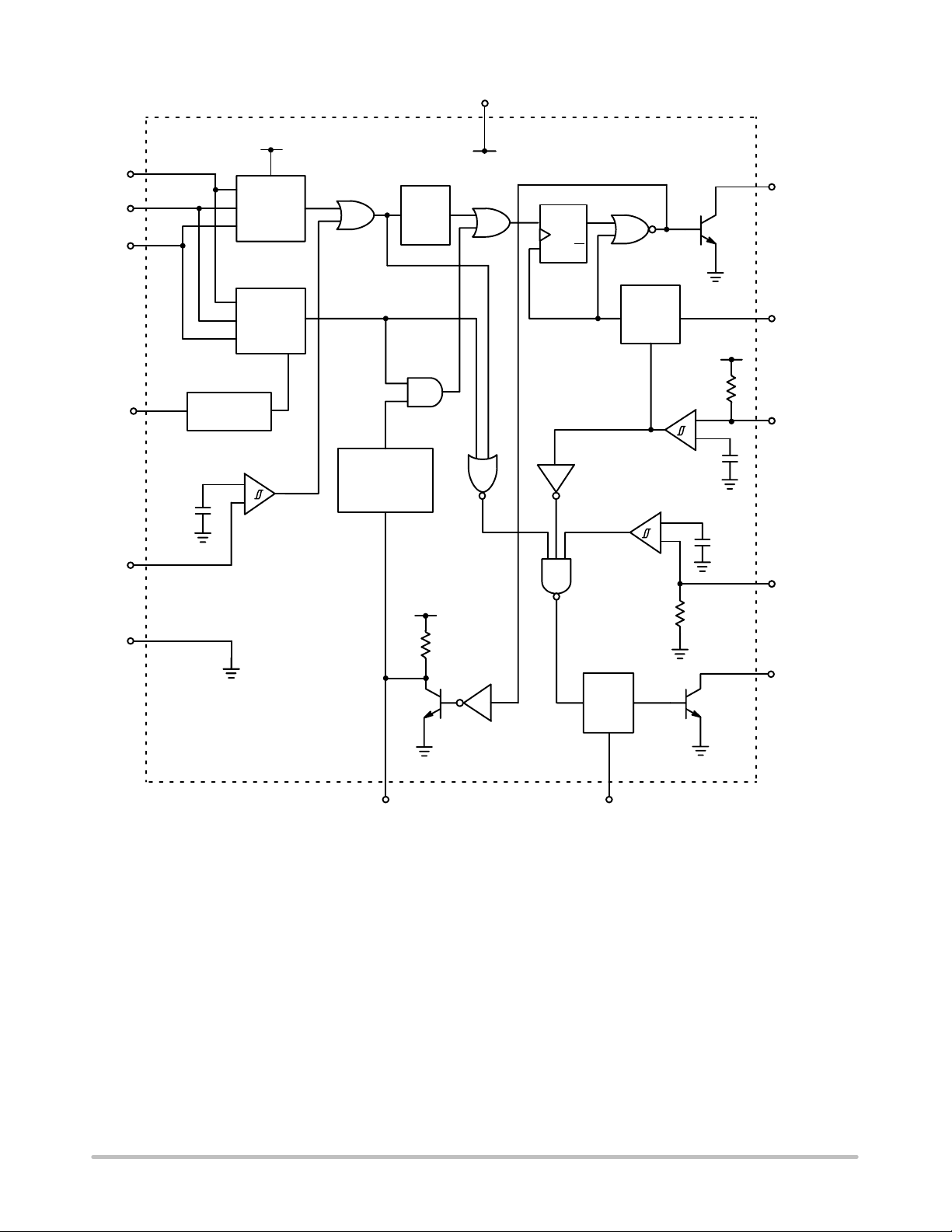
VS33
VS5
VS12
NCP112
V
CC
14
V
REF
1
2
OV
Detector
3
OV
Fault
Delay
V
CC
SET
SQ
RQ
CLR
13
FAULT
VREF
ADJ
GND
UV
Detector
Remote
On/Off
Delay
10
CTREMOTE
3.4 V
8
2.5 V
Reference
9
+
9
REMOTE
−
UV Blanking
Delay at
Power Up
1.28 V
+
−
4
1.28 V
−
+
1.28 V
5
5
PGI
V
V
CC
CC
7
12
Power
PGO
Good
Delay
6
CTUV
Figure 1. Block Diagram
http://onsemi.com
3
11
CTPG

NCP112
MAXIMUM RATINGS
Rating Symbol Value Unit
Power Supply Voltage (Note 1)
Power Good Output Current
Fault Output Current
Voltage Reference Output Current
V
CC
I
PGO
I
FAULT
I
REF
Voltage Rating (Pins 4, 5, 6, 9, 10, 11) ADJ, PGI, CTUV , REMOTE,
CTREMOTE, CTPG
Voltage Rating (Pins 12, 13) PGO, FAULT 18 V
Power Dissipation and Thermal Characteristics (PDIP−14)
Thermal Resistance, Junction−to−Air
Thermal Resistance, Junction−to−Case
Maximum Power Dissipation @ 25°C
R
JA
R
JC
P
D
Power Dissipation and Thermal Characteristics (SOIC−14)
Thermal Resistance, Junction−to−Air
Thermal Resistance, Junction−to−Case
Maximum Power Dissipation @ 25°C
Operating Junction Temperature
Operating Ambient Temperature
Storage Temperature Range
R
JA
R
JC
P
D
T
J
T
A
T
stg
18 V
30 mA
30 mA
20 mA
V
CC
100
45
1.25
125
30
1.0
+150 °C
−40 to +125 °C
−55 to +150 °C
V
°C/W
°C/W
W
°C/W
°C/W
W
ELECTRICAL CHARACTERISTICS (V
= 5.0 V , T
CC
= 25°C for typical values and TA = 0°C to 85°C for min and max values, unless
A
otherwise noted.)
Characteristic Symbol Min Typ Max Unit
OPERATING CONDITIONS
DC Power Supply V
Power Supply Current I
OVERVOLTAGE/UNDERVOLTAGE PROTECTION
Overvoltage Protection
3.3 V Output Sense
Hysteresis*
5.0 V Output Sense
Hysteresis*
12 V Output Sense
Hysteresis*
Undervoltage Protection
3.3 V Output Sense
Hysteresis*
5.0 V Output Sense
Hysteresis*
VOV33
VOV
VOV5
VOV
VOV12
VOV
VUV33
VUV
VUV5
VUV
CC
CC
hys33
hys5
hys12
hys33
hys5
4.5 − 16 V
− 3.0 5.0 mA
3.8
−
5.8
−
13.4
−
2.3
−
3.7
−
4.0
40
6.1
60
14.2
130
2.5
100
4.0
100
4.2
−
6.4
−
15
−
2.7
−
4.3
−
V
mV
V
mV
V
mV
V
mV
V
mV
12 V Output Sense
Hysteresis*
VUV12
VUV
hys12
9.2
10
−
100
*Hysteresis is measured in direction from threshold point back to nominal value of input voltage (i.e. 3.3 V , 5.0 V or 12 V).
1. This device contains ESD protection and exceeds the following tests:
Human Body Model JESD 22−A114−B: 2.0 kV
Machine Model JESD 22−A115−A: 200 V
http://onsemi.com
4
10.8
−
V
mV

NCP112
ELECTRICAL CHARACTERISTICS (continued) (V
= 5.0 V , T
CC
values, unless otherwise noted.)
Characteristic Symbol Min Typ Max Unit
OVERVOLTAGE/UNDERVOLTAGE PROTECTION (continued)
Undervoltage Protection (continued)
Adjustable Overvoltage Protection Threshold
Hysteresis
UNDERVOLTAGE BLANKING DURING POWER UP
Undervoltage Blanking Time (C
TUV
= 100 nF)
Undervoltage Blanking Threshold Voltage (Pin 6) T
POWER GOOD
Power Good Input Threshold Voltage
Power Good Input Hysteresis
Low State Open Collector Saturation Voltage
(I = 20 mA)
High State Open Collector Leakage Current
(V = 5.0 V)
Power Good Transient (See Application Note Section)
Rise Time
Fall Time
Adjustable Delay Time (C
TPG
= 100 nF)
Power Good Threshold Voltage (Pin 11) T
FAULT
Fault Sink Current I
Fault Saturation Voltage (I = 20 mA) V
Fault Leakage Current (V = 5.0 V) I
Fault Delay Time Before Latching T
REMOTE CONTROL
Remote Input Voltage Threshold
Remote Hysteresis
Remote Pin Internal Pull−Up Voltage V
Remote Low State Saturation Current I
Remote Time Delay (C
TREMOTE
= 100 nF)
Remote On
Remote Off
Remote Delay Threshold Voltage (Pin 10)
Low Level
High Level
VOLTAGE REFERENCE
Internal Voltage Reference (IO = 1.0 mA) @ 25°C
Internal Voltage Reference (IO = 1.0 mA) 0°C to 85°C
Line Regulation (4.5 V < V
CC
< 16 V)
Iout = 0 mA
Iout = 10 mA
Load Regulation (VCC = 5.0 V)
0 mA < Iout < 10 mA
= 25°C for typical values and TA = 0°C to 85°C for min and max
A
V
ADJth
V
ADJth
T
UV
UVth
V
PGIth
V
PGIhys
V
Lsat
I
Hleak
T
PGraise
T
PGfall
T
PG
PGth
FAULT
FAULTsat
FAULTleak
FAULT
V
Rth
V
Rhys
Rh
Rl
T
REMon
T
REMoff
T
REMth lo
T
REMth hi
V
REF
V
REF
V
REFline
V
REFline
V
REFload
−
−
1.28
100
−
−
100 300 500 ms
− 2.5 − V
−
−
1.28
25
−
−
− − 0.4 V
− − 1.0 A
−
−
1.0
1.0
−
−
100 300 500 ms
− 2.5 − V
20 − − mA
− − 0.4 V
− − 1.0 A
− 100 − s
−
−
1.28
25
−
−
3.3 3.4 3.6 V
− − 0.5 mA
35
35
−
−
2.46
2.42
−
−
45
45
0.2
2.3
2.50
2.50
4.0
15
60
60
−
−
2.54
2.58
10
−
− 25 − mV
V
mV
V
mV
s
V
mV
ms
V
V
mV
http://onsemi.com
5

V
CC
REMOTE
FAULT
PGI
PGO
NCP112
OVP
3.3 V, 5 V, 12 V
Tpg
Tremote (ON)
Tremote (OFF)
Tfault (OV)
Figure 2. Timing Diagram
T able 1. FUNCTION TABLE
PGI REMOTE ADJ Undervoltage Overvoltage FAULT PGO
<1.28 V (L) L <1.28 V (L) No No H L
<1.28 V (L) L <1.28 V (L) No Yes H L
<1.28 V (L) L <1.28 V (L) Yes No H L
<1.28 V (L) L >1.28 V (H) No No L L
<1.28 V (L) L >1.28 V (H) No Yes H L
<1.28 V (L) L >1.28 V (H) Yes No H L
>1.28 V (H) L <1.28 V (L) No No H L
>1.28 V (H) L <1.28 V (L) No Yes H L
>1.28 V (H) L <1.28 V (L) Yes No H L
>1.28 V (H) L >1.28 V (H) No No L H
>1.28 V (H) L >1.28 V (H) No Yes H L
>1.28 V (H) L >1.28 V (H) Yes No H L
X H X X X H L
2. X = > Don’t care.
3. FAULT = L means main PWM is Enable.
4. PGO = H means power supply is working within ATX specifications.
UVP
http://onsemi.com
6

NCP112
PRIMARY
RECTIFIER
MAIN
CONVERTER
PWM + OPTO
+ V
ref
AUXILIARY
CONVERTER
PWM + OPTO
+ V
ref
FAULT
12 V
5 V
3.3 V
V
CC
5 V STBY
NCP112
− Over and Undervoltage Protection
− Reference
− Logic
− Sequencer
12 V
5 V
3.3 V
5 V STBY
PG
REM
Figure 3. Simplified Application Schematic
http://onsemi.com
7

NCP112
PIN FUNCTION DESCRIPTION
Main Line Sensing − VS33, VS5 and VS12
These pins are used to monitor the main power outputs.
The internal circuitry of the NCP112 provides over and
undervoltage detection and indicates an error state. The
over and undervoltage levels meet the ATX specification.
In order to avoid unexpected oscillation of the device, the
NCP112 features both over and undervoltage hysteresis.
The overvoltage detection circuitry incorporates a fault
delay, which helps to filter short positive voltage spikes
below 100s. To avoid triggering a false undervoltage
signal during power−up, a timing capacitor (CTUV) may
be used to introduce a user defined blanking delay.
Additional Overvoltage Protection – ADJ
This pin can be used as another user−defined monitoring
input and has a hysteresis feature similar to VS33, VS5 and
VS12. When the input voltage is below the threshold level
of 1.28 V, a fault condition is asserted. Note that the ADJ
pin is logically ORed with the overvoltage detector output,
thus there is a 100s fault delay.
Power Good Input – PGI
The Power Good Input (PGI) can be used to monitor an
additional logic event, for example, the temperature inside
an ATX power supply unit. When the input voltage at the
PGI input is below the threshold level of 1.28 V, the Power
Good Output (PGO) signal remains in a low state, even if
all three sense inputs are within voltage limits. The PGI
signal, along with the REMOTE, and the over and
undervoltage singles encounter a power good delay circuit
as depicted in Figure 1.
Timing Capacitors – CTUV, CTREMOTE, CTPG
The NCP112 timing circuitry is optimized for utilizing
low cost, 100 nF ceramic capacitors. The time delays of
CTUV, CTREMOTE, and CTPG can be adjusted by simply
changing external capacitor values. The time delay is a
linear function of the capacitance because the NCP112 uses
internal current sources for charging and/or discharging
capacitors.
Remote Control – REMOTE
A reset signal can be realized with the REMOTE pin.
When the Remote pin is in the active low state, the external
link (the Fault signal) between the NCP112 and the Pulse
Width Modulator (PWM) generator of the external power
supply is enabled (Figure 3). In order to effectively reset
the latch, a minimum width remote pulse should be
applied. The width of this pulse should be greater than
T
, which is determined by adding an external capacitor
REM
(CTREMOTE). Note that the REMOTE pin is internally
pulled up to 3.4 V.
Power Good Output – PGO
The purpose of the PGO function is to warn the
motherboard that the voltage of at least one of the three
main power lines is out of range, independent of the ADJ
input. Please refer to Table 1 for a functional Truth table.
The PGO is subject to a delay TPG, which can be adjusted
with an external capacitor (CTPG). The Power Good
Output pin is capable of sinking 20 mA of current.
Fault Output – FAULT
In a typical application such as Figure 3, the fault pin
(FAULT), is activated when any one of the three main
power lines (3.3 V, 5.0 V, 12 V) is out of range or the ADJ
pin is below 1.28 V. This is independent of the PGI input.
The Fault output is the external link between the NCP112
and the primary PWM. In the event of a short circuit
condition, the overvoltage circuitry provides an additional
delay time T
Voltage Reference – VREF
which provides adequate protection.
FAULT
The VREF is a 2.5V precision reference output, with
current sourcing capability of 20 mA. No bypass capacitor
or minimum output current is required to maintain stability.
http://onsemi.com
8

−T−
SEATING
PLANE
14 8
17
N
HG
NCP112
PACKAGE DIMENSIONS
PDIP
P SUFFIX
CASE 646−06
ISSUE M
NOTES:
1. DIMENSIONING AND TOLERANCING PER ANSI
Y14.5M, 1982.
2. CONTROLLING DIMENSION: INCH.
B
A
F
L
C
D
14 PL
0.13 (0.005)
K
J
M
M
3. DIMENSION L TO CENTER OF LEADS WHEN
FORMED PARALLEL.
4. DIMENSION B DOES NOT INCLUDE MOLD
FLASH.
5. ROUNDED CORNERS OPTIONAL.
DIM MIN MAX MIN MAX
A 0.715 0.770 18.16 18.80
B 0.240 0.260 6.10 6.60
C 0.145 0.185 3.69 4.69
D 0.015 0.021 0.38 0.53
F 0.040 0.070 1.02 1.78
G 0.100 BSC 2.54 BSC
H 0.052 0.095 1.32 2.41
J 0.008 0.015 0.20 0.38
K 0.115 0.135 2.92 3.43
L
0.290 0.310 7.37 7.87
M −−− 10 −−− 10
N 0.015 0.039 0.38 1.01
MILLIMETERSINCHES
−T−
SEATING
PLANE
−A−
14 8
G
D 14 PL
0.25 (0.010) A
SOIC−14
D SUFFIX
CASE 751A−03
ISSUE F
NOTES:
1. DIMENSIONING AND TOLERANCING PER
ANSI Y14.5M, 1982.
2. CONTROLLING DIMENSION: MILLIMETER.
3. DIMENSIONS A AND B DO NOT INCLUDE
MOLD PROTRUSION.
4. MAXIMUM MOLD PROTRUSION 0.15 (0.006)
−B−
P 7 PL
M
71
0.25 (0.010) B
C
R X 45
K
M
S
B
T
S
M
M
F
J
PER SIDE.
5. DIMENSION D DOES NOT INCLUDE DAMBAR
PROTRUSION. ALLOWABLE DAMBAR
PROTRUSION SHALL BE 0.127 (0.005) TOTAL
IN EXCESS OF THE D DIMENSION AT
MAXIMUM MATERIAL CONDITION.
DIM MIN MAX MIN MAX
A 8.55 8.75 0.337 0.344
B 3.80 4.00 0.150 0.157
C 1.35 1.75 0.054 0.068
D 0.35 0.49 0.014 0.019
F 0.40 1.25 0.016 0.049
G 1.27 BSC 0.050 BSC
J 0.19 0.25 0.008 0.009
K 0.10 0.25 0.004 0.009
M 0 7 0 7
P 5.80 6.20 0.228 0.244
R 0.25 0.50 0.010 0.019
INCHESMILLIMETERS
http://onsemi.com
9

NCP112
ON Semiconductor and are registered trademarks of Semiconductor Components Industries, LLC (SCILLC). SCILLC reserves the right to make changes without further notice
to any products herein. SCILLC makes no warranty, representation or guarantee regarding the suitability of its products for any particular purpose, nor does SCILLC assume any
liability arising out of the application or use of any product or circuit, and specifically disclaims any and all liability, including without limitation special, consequential or incidental
damages. “Typical” parameters which may be provided in SCILLC data sheets and/or specifications can and do vary in different applications and actual performance may vary over
time. All operating parameters, including “Typicals” must be validated for each customer application by customer’s technical experts. SCILLC does not convey any license under
its patent rights nor the rights of others. SCILLC products are not designed, intended, or authorized for use as components in systems intended for surgical implant into the body,
or other applications intended to support or sustain life, or for any other application in which the failure of the SCILLC product could create a situation where personal injury or death
may occur. Should Buyer purchase or use SCILLC products for any such unintended or unauthorized application, Buyer shall indemnify and hold SCILLC and its officers, employees,
subsidiaries, affiliates, and distributors harmless against all claims, costs, damages, and expenses, and reasonable attorney fees arising out of, directly or indirectly, any claim of
personal injury or death associated with such unintended or unauthorized use, even if such claim alleges that SCILLC was negligent regarding the design or manufacture of the part.
SCILLC is an Equal Opportunity/Affirmative Action Employer. This literature is subject to all applicable copyright laws and is not for resale in any manner.
PUBLICATION ORDERING INFORMATION
LITERATURE FULFILLMENT:
Literature Distribution Center for ON Semiconductor
P.O. Box 5163, Denver, Colorado 80217 USA
Phone: 303−675−2175 or 800−344−3860 Toll Free USA/Canada
Fax: 303−675−2176 or 800−344−3867 Toll Free USA/Canada
Email: orderlit@onsemi.com
N. American Technical Support: 800−282−9855 Toll Free
USA/Canada
Japan: ON Semiconductor, Japan Customer Focus Center
2−9−1 Kamimeguro, Meguro−ku, Tokyo, Japan 153−0051
Phone: 81−3−5773−3850
http://onsemi.com
ON Semiconductor Website: http://onsemi.com
Order Literature: http://www.onsemi.com/litorder
For additional information, please contact your
local Sales Representative.
NCP112/D
10
 Loading...