How it Works
Log In / Sign Up
Buy Points
How it Works
FAQ
Contact Us
Questions and Suggestions
Users
ON Semiconductor
Loading...
N
NC7ST32
NC7SZ04
NC7SZ125
NC7SZ157
NC7SZ175
NC7SZ19
NC7SZ27
NC7SZ32
NC7SZ373
NC7SZ374
NC7SZU04
NC7WV04
NC7WV17
NC7WZ07
NC7WZ16
NCD5703A
NCD5703B
NCD5703C
NCD57085
NCD57090A,NCV57090A,NCD57091A,NCV57091A,NCD57090B,NCV57090B,NCD57091B,NCV57091B,NCD57090C,NCV57090C,NCD57091C,NCV57091C,NCD57090D,NCV57090D,NCD57091D,NCV57091D,NCD57090E,NCV57090E,NCD57091E,NCV57091E,NCD57090F,NCV57090F,NCD57091F,NCV57091F
NCD9830GEVB
NCL30073LED4GEVB
NCL30076
NCL35076
NCN4555
NCN49597
NCN51205GEVB
NCN5150QFNGEVB
NCN5150SOICGEVB
NCN5192NGEVB
NCN8024GEVB
NCP1010
NCP1011
NCP1012
NCP1013
NCP1014
NCP1027
NCP1030
NCP1031
NCP1050
NCP1051
NCP1052
NCP1053
NCP1054
NCP1055
NCP1060
3
NCP1063
2
NCP1083QBCGEVB
NCP1086
NCP1095GEVB
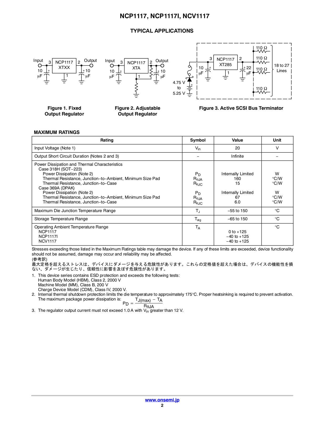
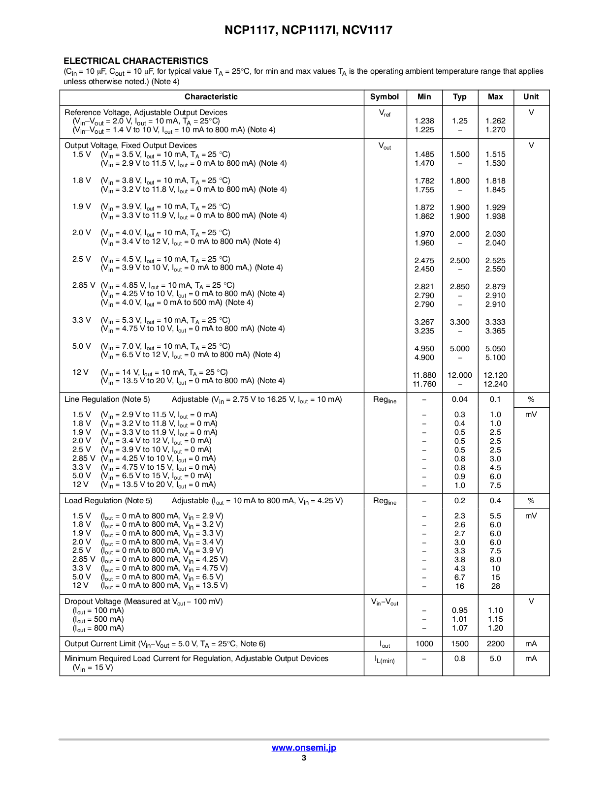
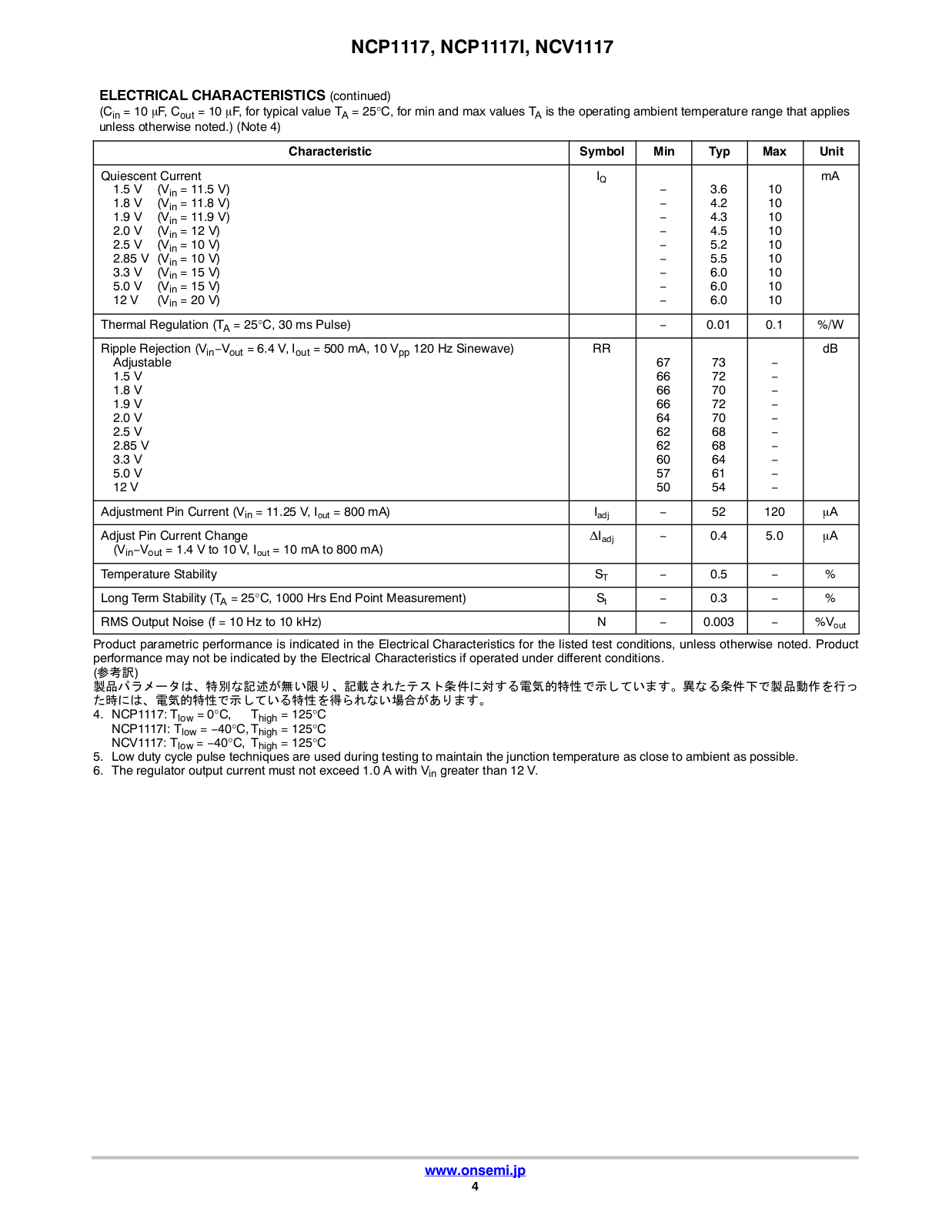
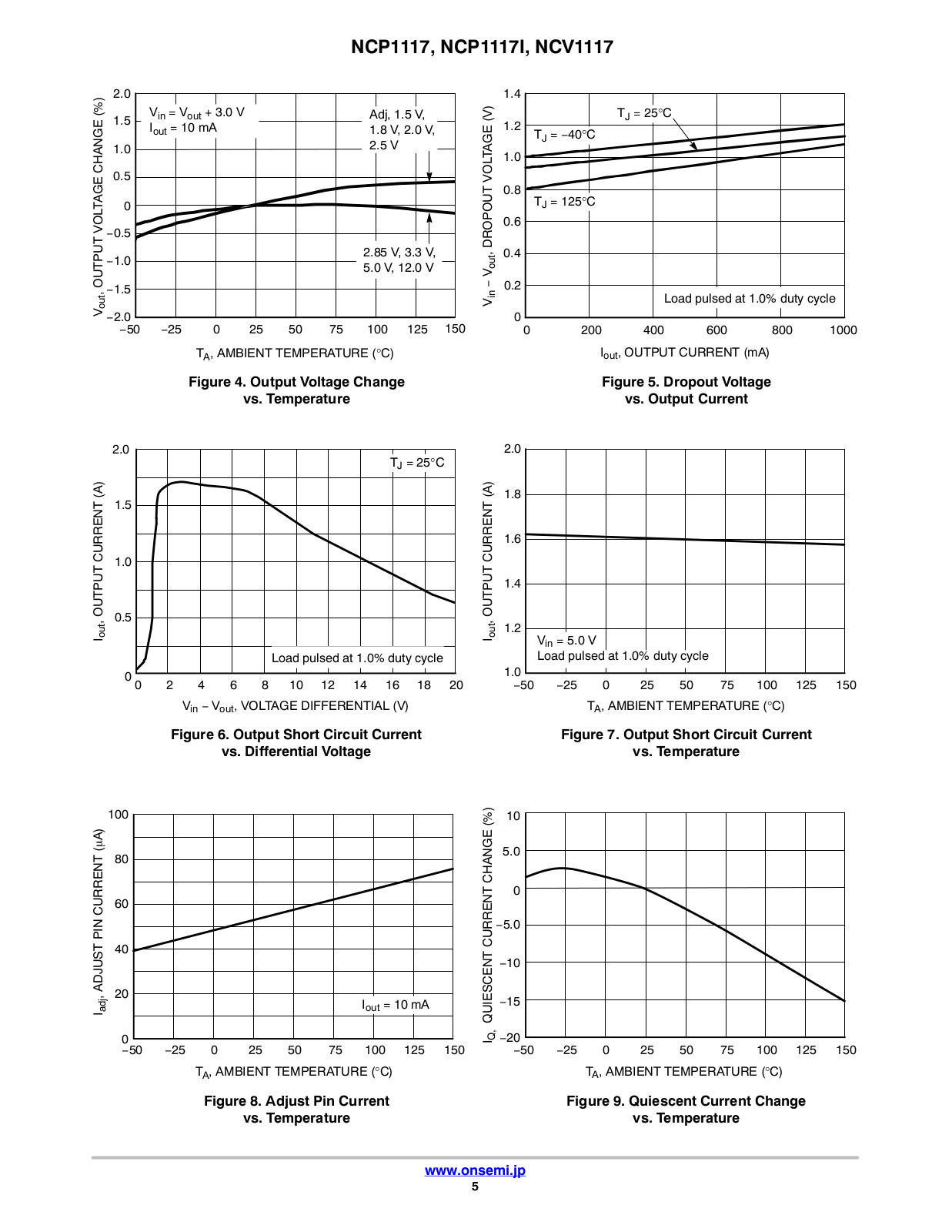
NCP1117
3
NCP1117I
2
NCP112
NCP1200
NCP1200A
NCP1200CH
NCP1201
NCP1215
NCP1219PRINTGEVB
NCP1239FDR2
NCP1239FDR2G
NCP1239VDR2
NCP1239VDR2G
NCP12400
NCP1308
NCP1337
NCP139
NCP1397A
NCP1397B
NCP13992MM240WGEVB
NCP1400A
NCP1402
NCP1404
NCP1450A
2
NCP1523
NCP1526
NCP1568D
NCP1568DC48WGEVB
NCP1608BOOSTGEVB
NCP1654
NCP1800
NCP1835B
NCP2811AMTTXGEVB
NCP2820
NCP2824FCT2GEVB
NCP300
NCP301
NCP302
NCP302150
NCP302155
NCP303
NCP3063
NCP3063B
NCP3065
NCP3163
NCP3218
NCP3284
NCP336
NCP337
NCP4305
Loading...
Loading...
Nothing found
NCP1117
Technical data
16 pgs
146.64 Kb
0
User manual
19 pgs
532.92 Kb
0
User Manual
19 pgs
386.91 Kb
0
Table of contents
Loading...
ON Semiconductor NCP1117, NCP1117I, NCV1117 User manual
...
ON Semiconductor User manual
Download
Specifications and Main Features
Frequently Asked Questions
User Manual
Download
Loading...
+
13
hidden pages
Unhide
You need points to download manuals.
1 point = 1 manual.
You can buy points or you can get point for every manual you upload.
Buy points
Upload your manuals