

查询MC33375D-2.5供应商
MC33375 Series
300 mA, Low Dropout
Voltage Regulator with
On/Off Control
The MC33375 series are micropower low dropout voltage
regulators available in a wide variety of output voltages as well as
packages, SOT−223 and SOP−8. These devices feature a very low
quiescent current and are capable of supplying output currents up to
300 mA. Internal current and thermal limiting protection are provided
by the presence of a short circuit at the output and an internal thermal
shutdown circuit.
The MC33375 has a control pin that allows a logic level signal to
turn−off or turn−on the regulator output.
Due to the low input−to−output voltage differential and bias current
specifications, these devices are ideally suited for battery powered
computer, consumer, and industrial equipment where an extension of
useful battery life is desirable.
Features:
• Low Quiescent Current (0.3 A in OFF mode; 125 A in ON mode)
• Low Input−to−Output Voltage Differential of 25 mV at I
and 260 mV at I
= 300 mA
O
• Extremely Tight Line and Load Regulation
• Stable with Output Capacitance of only 0.33 F for 2.5 V Output
Voltage
• Internal Current and Thermal Limiting
• Logic Level ON/OFF Control
• Pb−Free Packages are Available
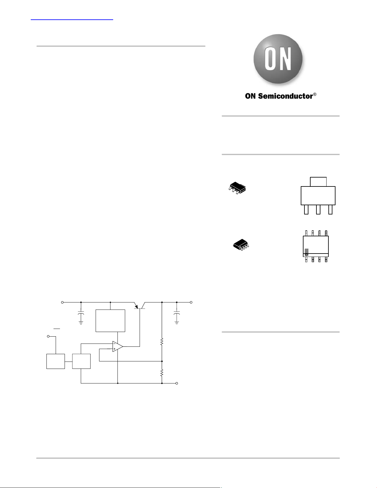
V
in
Thermal &
Anti−sat
On/Off
On/Off
Block
1.23 V
V. Ref.
Protection
Rint
54 K
O
GND
= 10 mA,
V
out
http://onsemi.com
LOW DROPOUT
MICROPOWER VOLTAGE
REGULATOR
MARKING
DIAGRAMS
4
SOT−223
ST SUFFIX
1
8
(Note: Microdot may be in either location)
See detailed ordering and shipping information in the
package dimensions section on page 11 of this data sheet.
CASE 318E
SOIC−8
1
D SUFFIX
CASE 751
A = Assembly Location
Y = Year
M = Date Code
L = Wafer Lot
W = Work Week
xx = Voltage Version
G = Pb−Free Package
ORDERING INFORMATION
AYM
375xx G
G
1
8
375xx
ALYW
G
1
This device contains 41 active transistors
Figure 1. Simplified Block Diagram
© Semiconductor Components Industries, LLC, 2006
October, 2006 − Rev. 10
1 Publication Order Number:
MC33375/D
MC33375 Series
PIN CONNECTIONS
Gnd
4
123
V
in
ON/
V
out
ON/OFF
Input
Gnd
Gnd
1
2
3
4
8
7
6
5
Output
Gnd
Gnd
N/C
OFF
MAXIMUM RATINGS
Rating Symbol Value Unit
Input Voltage V
CC
Power Dissipation and Thermal Characteristics
TA = 25°C
Maximum Power Dissipation
Case 751 (SOP−8) D Suffix
Thermal Resistance, Junction−to−Ambient
Thermal Resistance, Junction−to−Case
Case 318E (SOT−223) ST Suffix
Thermal Resistance, Junction−to−Air
Thermal Resistance, Junction−to−Case
Output Current I
Maximum Junction Temperature T
Operating Ambient Temperature Range T
Storage Temperature Range T
P
D
R
JA
R
JC
R
JA
R
JC
O
J
A
stg
Stresses exceeding Maximum Ratings may damage the device. Maximum Ratings are stress ratings only. Functional operation above the
Recommended Opera t i n g Conditions is not implied. Extended exposure to stresses above the Recommended Operating Conditions may affect
device reliability.
13 Vdc
Internally Limited
160
25
245
15
300 mA
150 °C
− 40 to +125 °C
− 65 to +150 °C
W
°C/W
°C/W
°C/W
°C/W
http://onsemi.com
2
MC33375 Series
ELECTRICAL CHARACTERISTICS (C
Characteristic
Output Voltage IO = 0 mA to 250 mA
1.8 V Suffix T
2.5 V Suffix
3.0 V Suffix
3.3 V Suffix
5.0 V Suffix
1.8 V Suffix V
2.5 V Suffix 2% Tolerance from T
3.0 V Suffix
3.3 V Suffix
5.0 V Suffix
Line Regulation Vin = [VO + 1] V to 12 V, IO = 250 mA,
Load Regulation Vin = [VO + 1] V, IO = 0 mA to 250 mA,
Dropout Voltage
= 10 mA TJ = −40°C to +125°C
I
O
= 100 mA
I
O
= 250 mA
I
O
= 300 mA
I
O
Ripple Rejection (120 Hz) V
Output Noise Voltage
C
= 1.0 FIO = 50 mA (10 Hz to 100 kHz)
L
C
= 200 F
L
= 25°C, Vin = [VO + 1] V
A
= [VO + 1] V, 0 < IO < 100 mA
in
All Suffixes T
All Suffixes T
= 25°C
A
= 25°C
A
in(peak−peak)
= 1.0 F, TA = 25°C, for min/max values TJ = −40°C to +125°C, Note 1)
L
Symbol Min Typ Max Unit
V
= −40 to +125°C
J
O
Reg
Reg
load
Vin − V
line
1.782
2.475
2.970
3.267
4.950
1.764
2.450
2.940
3.234
4.900
1.80
2.50
3.00
3.30
5.00
−
−
−
−
−
1.818
2.525
3.030
3.333
5.05
1.836
2.550
3.060
3.366
5.100
− 2.0 10 mV
− 5.0 25 mV
O
−
−
−
−
25
115
220
260
100
200
400
500
= [VO + 1.5] V to [VO + 5.5] V − 65 75 − dB
V
n
−
−
160
46
−
−
CURRENT PARAMETERS
Quiescent Current ON Mode Vin = [VO + 1] V, IO = 0 mA I
Quiescent Current OFF Mode I
Quiescent Current ON Mode SAT Vin = [VO − 0.5] V, IO = 0 mA (Note 2)
1.8 V Suffix
2.5 V Suffix
3.0 V Suffix
3.3 V Suffix
5.0 V Suffix
Current Limit Vin = [VO + 1] V, VO Shorted I
QOn
QOff
I
QSAT
LIMIT
− 125 200
− 0.3 4.0
−
−
−
−
−
1100
1100
1500
1500
1500
1500
1500
2000
2000
2000
− 450 − mA
ON/OFF INPUTS
On/Off Input Voltage
Logic “1” (Regulator On) V
Logic “0” (Regulator Off) V
Logic “0” (Regulator Off) V
= VO ± 2%
out
< 0.03 V
out
< 0.05 V (1.8 V Option)
out
V
CTRL
2.4
−
−
−
−
−
−
0.5
0.3
THERMAL SHUTDOWN
Thermal Shutdown − − 150 − °C
1. Low duty pulse techniques are used during test to maintain junction temperature as close to ambient as possible.
2. Quiescent Current is measured where the PNP pass transistor is in saturation. V
= [VO − 0.5] V guarantees this condition.
in
Vdc
mV
Vrms
A
A
A
V
http://onsemi.com
3

MC33375 Series
DEFINITIONS
Load Regulation − The change in output voltage for a
change in load current at constant chip temperature.
Dropout Voltage − The input/output differential at which
the regulator output no longer maintains regulation against
further reductions in input voltage. Measured when the
output drops 100 mV below its nominal value (which is
measured at 1.0 V differential), dropout voltage is affected
by junction temperature, load current and minimum input
supply requirements.
Output Noise Voltage − The RMS AC voltage at the
output with a constant load and no input ripple, measured
over a specified frequency range.
Maximum Power Dissipation − The maximum total
dissipation for which the regulator will operate within
specifications.
Quiescent Current − Current which is used to operate the
regulator chip and is not delivered to the load.
Line Regulation − The change in output voltage for a
change in the input voltage. The measurement is made under
conditions of low dissipation or by using pulse techniques
such that the average chip temperature is not significantly
affected.
Maximum Package Power Dissipation − The maximum
package power dissipation is the power dissipation level at
which the junction temperature reaches its maximum value
i.e. 150°C. The junction temperature is rising while the
difference between the input power (V
output power (V
out
X I
out
) is increasing.
X ICC) and the
CC
Depending on ambient temperature, it is possible to
calculate the maximum power dissipation and so the
maximum current as following:
TJ–T
R
A
JA
Pd +
The maximum operating junction temperature TJ is
specified at 150°C, if T
= 25°C, then PD can be found. By
A
neglecting the quiescent current, the maximum power
dissipation can be expressed as:
P
I
out
+
D
VCC–V
out
The thermal resistance of the whole circuit can be
evaluated by deliberately activating the thermal shutdown
of the circuit (by increasing the output current or raising the
input voltage for example).
Then you can calculate the power dissipation by
subtracting the output power from the input power. All
variables are then well known: power dissipation, thermal
shutdown temperature (150°C for MC33375) and ambient
temperature.
TJ–T
R
JA
+
A
P
D
http://onsemi.com
4
MC33375 Series
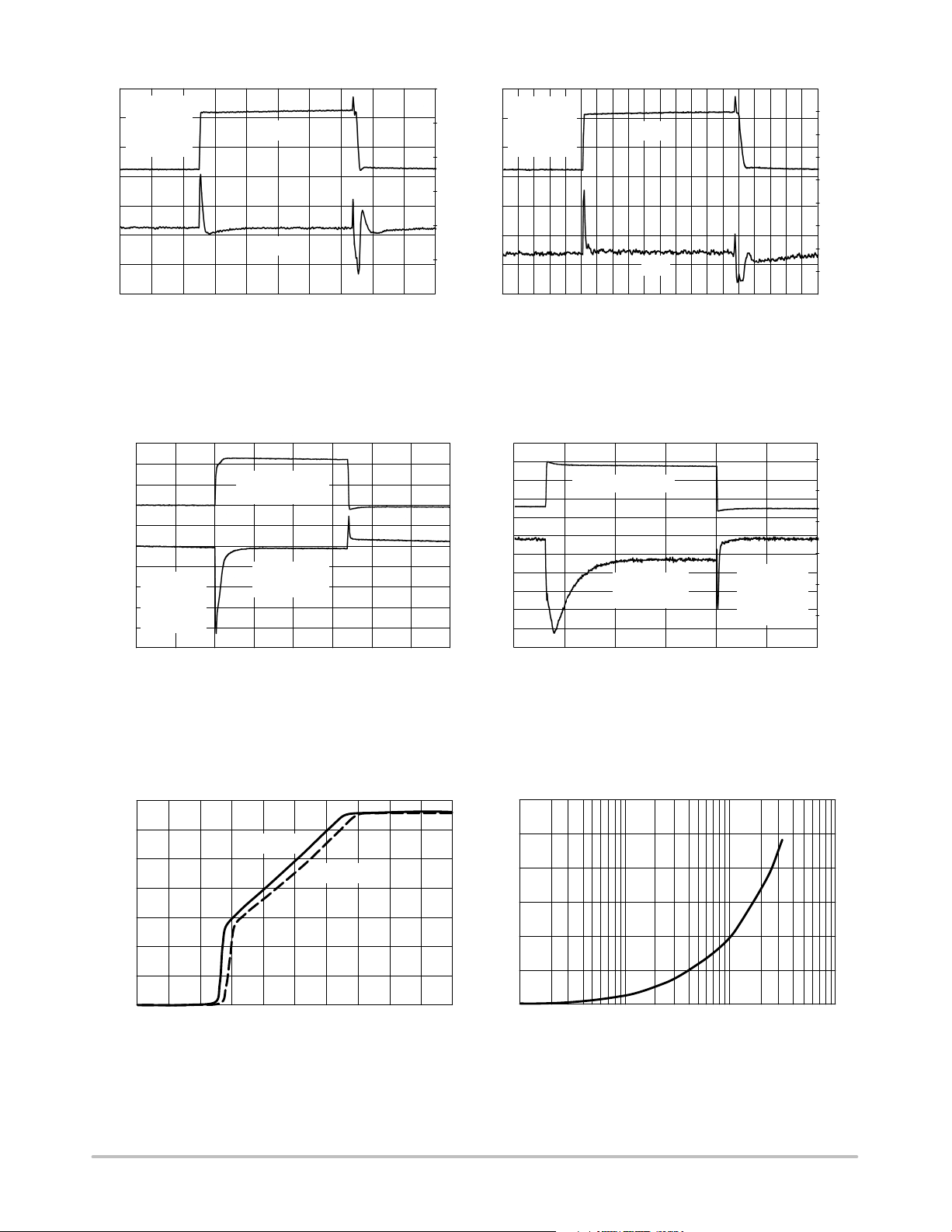
7
TA = 25° C
6
= 0.47 F
C
5
L
I
= 10 mA
L
V
= 3.3 V
out
V
in
4
3
, INPUT VOLTAGE (V)
2
in
V
V
out
1
0
0
20 40 60 80 100 120 140 160 180 200
TIME (S)
Figure 2. Line Transient Response Figure 3. Line Transient Response
300
200
100
0
LOAD
CURRENT
−100
−200
−300
−400
LOAD CURRENT (mA)
−500
−600
−700
CL = 1.0 F
V
= 3.3 V
out
T
= 25° C
A
V
= 4.3 V
in
0
50 100 150 200 250 400
V
out
CHANGE
TIME (S)
Figure 4. Load Transient Response
300 350
200
OUTPUT VOLTAGE CHANGE (mV)
150
100
50
0
−50
−100
1.0
0.8
OUTPUT VOLTAGE CHANGE (V)
0.6
0.4
0.2
0
−0.2
−0.4
−0.6
−0.8
−1.0
7
TA = 25° C
6
= 33 F
C
5
L
I
= 10 mA
L
V
= 3.3 V
out
V
in
4
3
2
, INPUT VOLTAGE (V)
in
V
1
V
out
0
0
50 100 150 200
TIME (S)
350
250
150
50
−50
−150
−250
−350
−450
LOAD CURRENT (mA)
−550
−650
−750
0 250 300
LOAD CURRENT
V
out
CHANGE
50 100 150
200
CL = 33.0 F
V
out
TA = 25° C
V
in
TIME (S)
Figure 5. Load Transient Response
= 3.3 V
= 4.3 V
70
OUTPUT VOLTAGE CHANGE (mV)
60
50
40
30
20
10
0
−10
−20
0.14
OUTPUT VOLTAGE CHANGE (V)
0.09
0.04
−0.01
−0.06
−0.11
−0.16
3.5
3.0
IL = 1 mA
2.5
IL = 250 mA
2.0
1.5
1.0
OUTPUT VOLTAGE (V)
0.5
0
0.5
0
1.0
1.5 2.0
2.5
3.0 3.5 4.0
INPUT VOLTAGE (V)
Figure 6. Output Voltage versus Input Voltage
300
250
200
150
100
DROPOUT VOLTAGE (mV)
50
0
4.5
5.0
1
Figure 7. Dropout Voltage versus Output Current
http://onsemi.com
5
10 100 1000
IO, OUTPUT CURRENT (mA)

MC33375 Series
300
250
200
150
100
DROPOUT VOLTAGE (mV)
50
0
−40
IL = 300 mA
IL = 250 mA
IL = 100 mA
IL = 10 mA
02585
TEMPERATURE (°C)
Figure 8. Dropout Voltage versus Temperature
8
7
6
5
(mA)
4
gnd
I
3
2
1
0
−40
−20
20
0
60 80 100
40
TA (°C)
Figure 10. Ground Pin Current versus
Ambient Temperature
IL = 250 mA
IL = 100 mA
IL = 50 mA
120
140
gnd
I (mA)
(VOLTS)
out
V
12
10
2.5
2.495
2.49
2.485
2.48
2.475
2.47
8
6
4
2
0
0
1
IL = 300 mA
IL = 100 mA
= 50 mA
I
L
23 8
45 67
(VOLTS)
V
in
Figure 9. Ground Pin Current versus
Input Voltage
IO = 0
IO = 250 mA
−40
02585
TEMPERATURE (°C)
Figure 11. Output Voltage versus Ambient
Temperature (V
= V
+ 1V)
in
out
http://onsemi.com
6

2.5
2.495
2.49
MC33375 Series
IO = 0
dB
−40
IO = 250 mA
02585
TEMPERATURE (°C)
(VOLTS)
out
V
2.485
2.48
2.475
2.47
2.465
Figure 12. Output Voltage versus Ambient
Temperature (V
70
60
50
40
30
20
10
0
0.1
1 10 100
FREQUENCY (kHz)
IL = 1 mA
IL = 10 mA
= 12 V)
in
70
60
50
40
dB
30
20
10
0
0.1
IL = 100 mA
IL = 250 mA
1 10 100
FREQUENCY (kHz)
Figure 13. Ripple Rejection Figure 14. Ripple Rejection
4.5
3.5
2.5
VOLTAGE (V)
1.5
0.5
5
4
3
2
1
0
0
ENABLE
CL = 1.0 F
CL = 33 F
TIME (S)
Figure 15. Enable Transient
http://onsemi.com
7
300
500100 200 400

MC33375 Series
1.8 V Option
1.85
I
1.84
LOAD
= 100 mA
1.83
1.82
1.81
1.80
1.79
, OUTPUT VOLTAGE (V)
1.78
OUT
1.77
V
1.76
1.75
−40
−20 0 20 40 60 80 100 120
TA, AMBIENT TEMPERATURE (°C)
Figure 16. Output Voltage versus Temperature Figure 17. Output Voltage versus Input Voltage
2.0
1.8
1.6
1.4
1.2
1.0
0.8
, OUTPUT VOLTAGE (V)
0.6
OUT
0.4
V
0.2
0
TA = 25° C
I
LOAD
0
1346
2
VCC, (V)
= 0 mA
5
12
10
TA = 25° C
V
= 3 V
CC
, (mA)
gnd
I
8
6
4
2
0
50 100 150 200 250 300 350
0
I
, (mA)
LOAD
Figure 18. Ground Current versus Load Current
80
70
60
50
40
PSRR (dB)
30
20
10
0
0.1
110
100 1000
f, FREQUENCY (kHz)
Figure 20. PSRR versus Frequency
140
120
100
80
( A)
Q
I
60
40
20
TA = 25° C
I
= 0 mA
LOAD
0
0
1346
2
5
VCC, (V)
Figure 19. Quiescent Current versus Input Voltage
VCC = 3 V
I
= 1 mA
LOAD
= 25°C
T
A
C
= 1 F
OUT
2 V
ENABLE
V
OUT
0 V
0 5 10 15 20 25 30 35 40 45 50
t, TIME (s)
Figure 21. Enable Response
http://onsemi.com
8

MC33375 Series
0
out
VCC = 3 V
I
= 1 mA to 100 mA
LOAD
= 25°C
T
A
1.82 V
1.80 V
1.78 V
100 mA
1 mA
0 0.5 1 1.5 2 2.5 3 3.5 4 4.5 5
t, TIME (ms)
Figure 22. Load Transient Response
APPLICATIONS INFORMATION
ON/OFF
V
in
MC33375−xx
C
in
Figure 23. Typical Application Circuit
The MC33375 regulators are designed with internal
current limiting and thermal shutdown making them
user−friendly. Figure 15 is a typical application circuit. The
output capability of the regulator is in excess of 300 mA,
with a typical dropout voltage of less than 260 mV. Internal
protective features include current and thermal limiting.
EXTERNAL CAPACITORS
These regulators require only a 0.33 F (or greater)
capacitance between the output and ground for stability for
1.8 V, 2.5 V, 3.0 V, and 3.3 V output voltage options. Output
voltage options of 5.0 V require only 0.22 F for stability.
The output capacitor must be mounted as close as possible
to the MC33375. If the output capacitor must be mounted
further than two centimeters away from the MC33375, then
a larger value of output capacitor may be required for
stability . A value of 0.68 F or la rger is recommended. Most
type of aluminum, tantalum, or multilayer ceramic will
perform adequately. Solid tantalums or appropriate
multilayer ceramic capacitors are recommended for
operation below 25°C. An input bypass capacitor is
recommended to improve transient response or if the
regulator is connected to the supply input filter with long
wire lengths, more than 4 inches. This will reduce the
circuit’s sensitivity to the input line impedance at high
V
out
out
GND
LOADC
frequencies. A 0.33 F or larger tantalum, mylar, ceramic,
or other capacitor having low internal impedance at high
frequencies should be chosen. The bypass capacitor should
be mounted with shortest possible lead or track length
directly across the regulator’s input terminals. Figure 16
shows the ESR that allows the LDO to remain stable for
various load currents.
100
10
ESR (ohm)
1.0
0.1
0
50 150 250
Figure 24. ESR for V
Applications should be tested over all operating
conditions to insure stability.
Stable Region
100 200 30
LOAD CURRENT (mA)
= 3.0V
V
out
C
out
C
= 1.0 F
in
= 3.0 V
= 1.0 F
http://onsemi.com
9

MC33375 Series
THERMAL PROTECTION
Internal thermal limiting circuitry is provided to protect
the integrated circuit in the event that the maximum junction
temperature is exceeded. When activated, typically at
150°C, the output is disabled. There is no hysteresis built
into the thermal protection. As a result the output will appear
to be oscillating during thermal limit. The output will turn
off until the temperature drops below the 150°C then the
output turns on again. The process will repeat if the junction
increases above the threshold. This will continue until the
existing conditions allow the junction to operate below the
temperature threshold.
Thermal limit is not a substitute for proper
heatsinking.
180
160
140
120
100
, THERMAL RESISTANCE,
JA
JUNCTION−TO−AIR (°CW)
R
Minimum
Size Pad
80
60
010203025155.0
P
for TA = 50°C
D(max)
L, LENGTH OF COPPER (mm)
The internal current limit will typically limit current to
450 mA. If during current limit the junction exceeds 150°C,
the thermal protection will protect the device also. Current
limit is not a substitute for proper heatsinking.
OUTPUT NOISE
In many applications it is desirable to reduce the noise
present at the output. Reducing the regulator bandwidth by
increasing the size of the output capacitor will reduce the
noise on the MC33375.
ON/OFF PIN
When this pin is pulled low, the MC33375 is off. This pin
should not be left floating. The pin should be pulled high for
the MC33375 to operate.
1.6
1.4
2.0 oz. Copper
L
L
R
JA
1.2
1.0
0.8
0.6
0.4
, MAXIMUM POWER DISSIPATION (W)
D
P
Figure 25. SOT−223 Thermal Resistance and Maximum
Power Dissipation versus P.C.B. Copper Length
170
150
130
JUNCTION-TO-AIR ( C/W)°
110
90
70
50
30
JAθ
R , THERMAL RESISTANCE,
02040503010
R
JA
L, LENGTH OF COPPER (mm)
P
for TA = 50°C
D(max)
Graph Represents Symmetrical Layout
2.0 oz.
L
Copper
L
3.0
mm
Figure 26. SOP−8 Thermal Resistance and Maximum
Power Dissipation versus P.C.B. Copper Length
3.2
2.8
2.4
2.0
1.6
1.2
0.8
0.4
http://onsemi.com
10
MC33375 Series
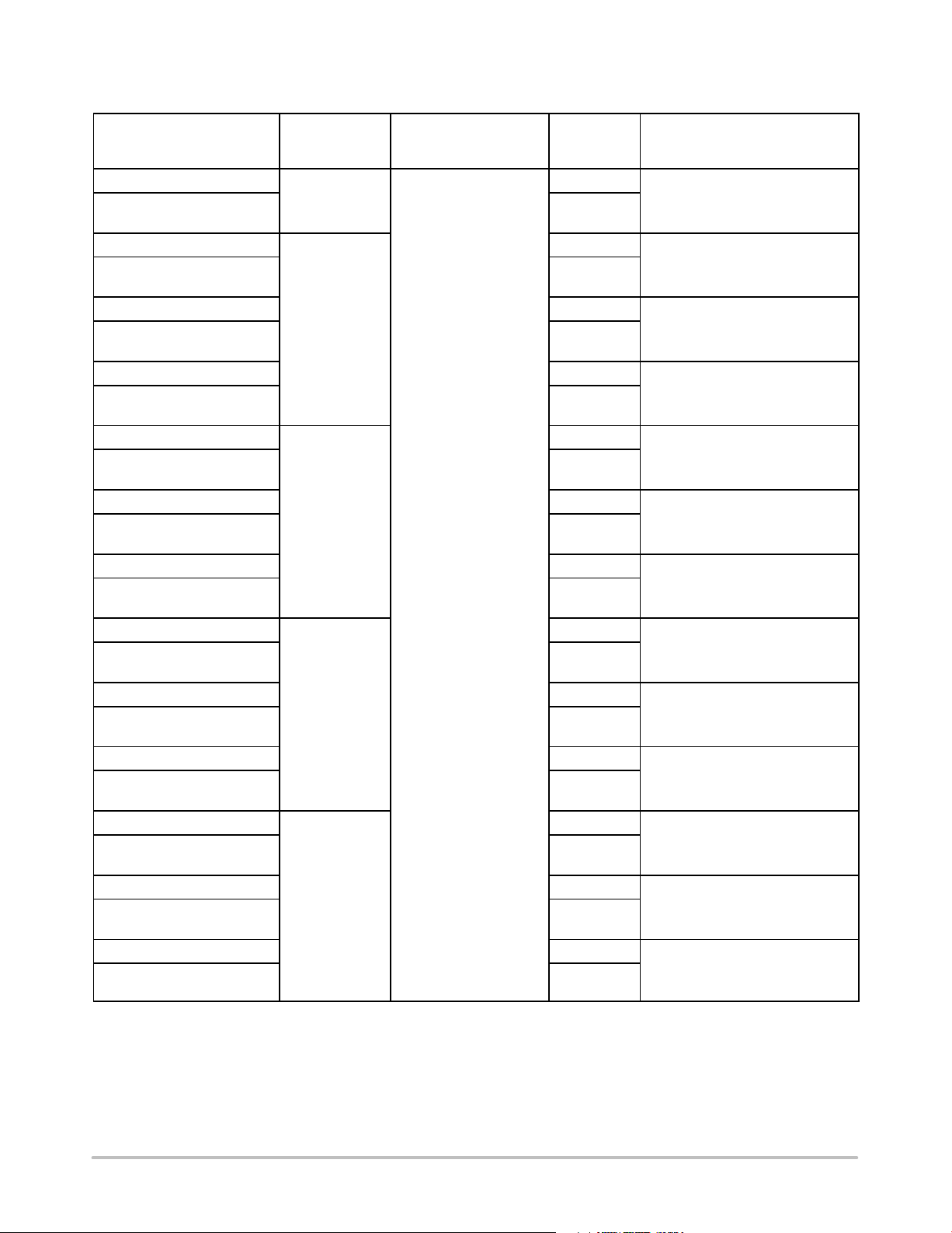
ORDERING INFORMATION
Operating
Temperature Range,
Device Type
MC33375ST−1.8T3
MC33375ST−1.8T3G SOT−223
MC33375D−2.5
MC33375D−2.5G SOIC−8
MC33375D−2.5R2 SOIC−8
MC33375D−2.5R2G SOIC−8
MC33375ST−2.5T3 SOT−223
MC33375ST−2.5T3G SOT−223
MC33375D−3.0
MC33375D−3.0G SOIC−8
MC33375D−3.0R2 SOIC−8
MC33375D−3.0R2G 1% Tolerance
MC33375ST−3.0T3 SOT−223
MC33375ST−3.0T3G 2% Tolerance at
MC33375D−3.3
MC33375D−3.3G SOIC−8
MC33375D−3.3R2 SOIC−8
MC33375D−3.3R2G SOIC−8
MC33375ST−3.3T3 SOT−223
MC33375ST−3.3T3G SOT−223
MC33375D−5.0
MC33375D−5.0G SOIC−8
MC33375D−5.0R2 SOIC−8
MC33375D−5.0R2G SOIC−8
MC33375ST−5.0T3 SOT−223
MC33375ST−5.0T3G SOT−223
†For information on tape and reel specifications, including part orientation and tape sizes, please refer to our Tape and Reel Packaging
Specifications Brochure, BRD8011/D.
1.8 V
(Fixed Voltage)
2.5 V
(Fixed Voltage)
3.0 V
(Fixed Voltage)
3.3 V
(Fixed Voltage)
5.0 V
(Fixed Voltage)
Tolerance
= 25°C
at T
A
from −40 to +125°C
T
J
Package Shipping
SOT−223
4000 / Tape & Reel
(Pb−Free)
SOIC−8
98 Units / Rail
(Pb−Free)
2500 / Tape & Reel
(Pb−Free)
4000 / Tape & Reel
(Pb−Free)
SOIC−8
98 Units / Rail
(Pb−Free)
SOIC−8
(Pb−Free)
SOT−223
(Pb−Free)
SOIC−8
(Pb−Free)
(Pb−Free)
(Pb−Free)
SOIC−8
(Pb−Free)
(Pb−Free)
(Pb−Free)
2500 / Tape & Reel
4000 / Tape & Reel
98 Units / Rail
2500 / Tape & Reel
4000 / Tape & Reel
98 Units / Rail
2500 / Tape & Reel
4000 / Tape & Reel
†
http://onsemi.com
11

MC33375 Series
DEVICE MARKING
Device Version Marking (1st line)
MC33375 1.8 V 37518
MC33375 2.5 V 37525
MC33375 3.0 V 37530
MC33375 3.3 V 37533
MC33375 5.0 V 37550
TAPE AND REEL SPECIFICATIONS
Device Reel Size Tape Width Quantity
MC33375D 13″ 12 mm Embossed Tape 2500 Units
MC33375ST 13″ 8 mm Embossed Tape 4000 Units
†For information on tape and reel specifications, including part orientation and tape sizes, please refer to our Tape and Reel Packaging
Specifications Brochure, BRD8011/D.
†
http://onsemi.com
12
MC33375 Series
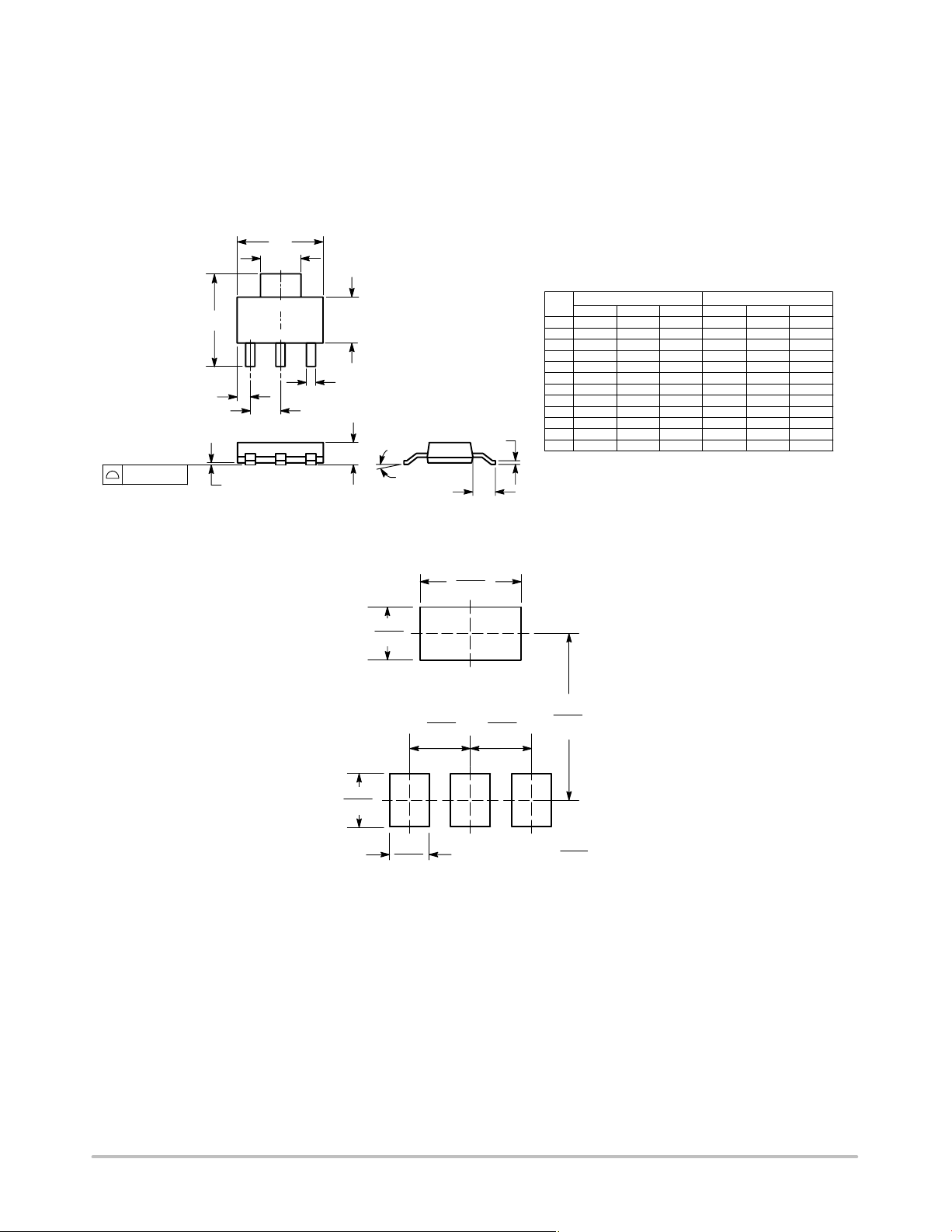
PACKAGE DIMENSIONS
SOT−223 (TO−261)
CASE 318E−04
ISSUE L
0.08 (0003)
H
e1
E
A1
D
b1
4
123
e
E
b
q
A
SOLDERING FOOTPRINT*
2.0
0.079
3.8
0.15
L1
NOTES:
1. DIMENSIONING AND TOLERANCING PER ANSI
Y14.5M, 1982.
2. CONTROLLING DIMENSION: INCH.
DIMAMIN NOM MAX MIN
A1 0.02 0.06 0.10 0.001
b 0.60 0.75 0.89 0.024
b1 2.90 3.06 3.20 0.115
c 0.24 0.29 0.35 0.009
D 6.30 6.50 6.70 0.249
E 3.30 3.50 3.70 0.130
e 2.20 2.30 2.40 0.087
e1
L1 1.50 1.75 2.00 0.060
H
C
E
q
MILLIMETERS
1.50 1.63 1.75 0.060
0.85 0.94 1.05 0.033
6.70 7.00 7.30 0.264
0° 10° 0° 10°
− −
INCHES
NOM MAX
0.064 0.068
0.002 0.004
0.030 0.035
0.121 0.126
0.012 0.014
0.256 0.263
0.138 0.145
0.091 0.094
0.037 0.041
0.069 0.078
0.276 0.287
2.3
0.091
2.3
0.091
6.3
0.248
2.0
0.079
1.5
0.059
SCALE 6:1
ǒ
inches
mm
Ǔ
*For additional information on our Pb−Free strategy and soldering
details, please download the ON Semiconductor Soldering and
Mounting Techniques Reference Manual, SOLDERRM/D.
http://onsemi.com
13

−Y−
−Z−
MC33375 Series
PACKAGE DIMENSIONS
SOIC−8 NB
CASE 751−07
ISSUE AH
NOTES:
−X−
A
58
B
1
S
0.25 (0.010)
4
M
M
Y
K
G
C
SEATING
PLANE
0.10 (0.004)
H
D
0.25 (0.010) Z
M
Y
SXS
N
X 45
_
M
J
1. DIMENSIONING AND TOLERANCING PER
ANSI Y14.5M, 1982.
2. CONTROLLING DIMENSION: MILLIMETER.
3. DIMENSION A AND B DO NOT INCLUDE
MOLD PROTRUSION.
4. MAXIMUM MOLD PROTRUSION 0.15 (0.006)
PER SIDE.
5. DIMENSION D DOES NOT INCLUDE DAMBAR
PROTRUSION. ALLOWABLE DAMBAR
PROTRUSION SHALL BE 0.127 (0.005) TOTAL
IN EXCESS OF THE D DIMENSION AT
MAXIMUM MATERIAL CONDITION.
6. 751−01 THRU 751−06 ARE OBSOLETE. NEW
STANDARD IS 751−07.
MILLIMETERS
DIMAMIN MAX MIN MAX
4.80 5.00 0.189 0.197
B 3.80 4.00 0.150 0.157
C 1.35 1.75 0.053 0.069
D 0.33 0.51 0.013 0.020
G 1.27 BSC 0.050 BSC
H 0.10 0.25 0.004 0.010
J 0.19 0.25 0.007 0.010
K 0.40 1.27 0.016 0.050
M 0 8 0 8
____
N 0.25 0.50 0.010 0.020
S 5.80 6.20 0.228 0.244
INCHES
SOLDERING FOOTPRINT*
1.52
0.060
7.0
0.275
0.6
0.024
*For additional information on our Pb−Free strategy and soldering
details, please download the ON Semiconductor Soldering and
Mounting Techniques Reference Manual, SOLDERRM/D.
ON Semiconductor and are registered trademarks of Semiconductor Components Industries, LLC (SCILLC). SCILLC reserves the right to make changes without further notice
to any products herein. SCILLC makes no warranty, representation or guarantee regarding the suitability of its products for any particular purpose, nor does SCILLC assume any liability
arising out of the application or use of any product or circuit, and specifically disclaims any and all liability, including without limitation special, consequential or incidental damages.
“Typical” parameters which may be provided in SCILLC data sheets and/or specifications can and do vary in different applications and actual performance may vary over time. All
operating parameters, including “Typicals” must be validated for each customer application by customer’s technical experts. SCILLC does not convey any license under its patent rights
nor the rights of others. SCILLC products are not designed, intended, or authorized for use as components in systems intended for surgical implant into the body, or other applications
intended to support or sustain life, or for any other application in which the failure of the SCILLC product could create a situation where personal injury or death may occur. Should
Buyer purchase or use SCILLC products for any such unintended or unauthorized application, Buyer shall indemnify and hold SCILLC and its officers, employees, subsidiaries, affiliates,
and distributors harmless against all claims, costs, damages, and expenses, and reasonable attorney fees arising out of, directly or indirectly, any claim of personal injury or death
associated with such unintended or unauthorized use, even if such claim alleges that SCILLC was negligent regarding the design or manufacture of the part. SCILLC is an Equal
Opportunity/Affirmative Action Employer. This literature is subject to all applicable copyright laws and is not for resale in any manner.
4.0
0.155
1.270
0.050
SCALE 6:1
ǒ
inches
mm
Ǔ
PUBLICATION ORDERING INFORMATION
LITERATURE FULFILLMENT:
Literature Distribution Center for ON Semiconductor
P.O. Box 5163, Denver, Colorado 80217 USA
Phone: 303−675−2175 or 800−344−3860 Toll Free USA/Canada
Fax: 303−675−2176 or 800−344−3867 Toll Free USA/Canada
Email: orderlit@onsemi.com
N. American Technical Support: 800−282−9855 Toll Free
USA/Canada
Europe, Middle East and Africa Technical Support:
Phone: 421 33 790 2910
Japan Customer Focus Center
Phone: 81−3−5773−3850
http://onsemi.com
14
ON Semiconductor Website: www.onsemi.com
Order Literature: http://www.onsemi.com/orderlit
For additional information, please contact your local
Sales Representative
MC33375/D
 Loading...