

查询MC33269D-3.3供应商
MC33269, NCV33269
800 mA, Adjustable Output,
Low Dropout Voltage
Regulator
The MC33269/NCV33269 series are low dropout, medium current,
fixed and adjustable, positive voltage regulators specifically designed
for use in low input voltage applications. These devices offer the
circuit designer an economical solution for precision voltage
regulation, while keeping power losses to a minimum.
The regulator consists of a 1.0 V dropout composite PNP−NPN pass
transistor, current limiting, and thermal shutdown.
• 3.3 V, 5.0 V, 12 V and Adjustable Versions.
2.85 V version available as MC34268.
• Space Saving DPAK, SOP−8 and SOT−223 Power Packages
• 1.0 V Dropout
• Output Current in Excess of 800 mA
• Thermal Protection
• Short Circuit Protection
• Output Trimmed to 1.0% Tolerance
• Pb−Free Package is Available
DEVICE TYPE/NOMINAL OUTPUT VOLTAGE
MC33269D
MC33269DT
NCV33269DTRK*
MC33269T
MC33269D−3.3
MC33269DT−3.3
NCV33269DTRK−3.3*
MC33269T−3.3
MC33269ST−3.3
*NCV prefix is for automotive and other applications requiring site and change
control.
Adj
Adj
Adj
Adj
3.3 V
3.3 V
3.3 V
3.3 V
3.3 V
MC33269D−5.0
MC33269DT−5.0
MC33269T−5.0
MC33269D−12
MC33269DT−12
NCV33269DTRK−12*
MC33269T−12
5.0 V
5.0 V
5.0 V
12 V
12 V
12 V
12 V
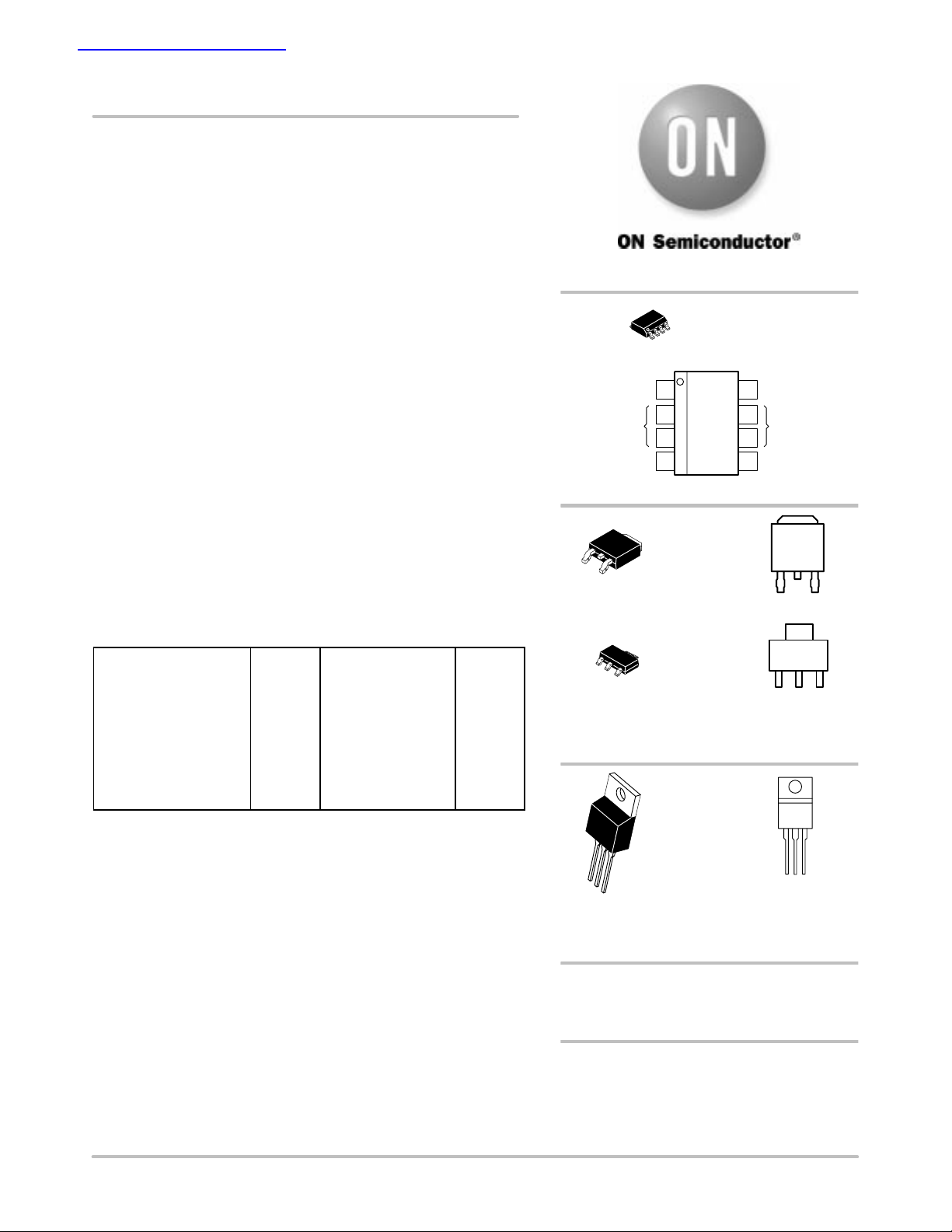
http://onsemi.com
out
in
SO−8
D SUFFIX
CASE 751
NC
8
7
V
6
NC
5
(Top View)
(Top View)
out
1
123
8
1
Gnd/Adj
V
1
3
1
3
Heatsink surface (shown as terminal 4 in
case outline drawing) is connected to Pin 2.
out
V
in
1
2
3
4
(Top View)
DPAK
DT SUFFIX
CASE 369A
1. GND/Adj
2. V
3. V
SOT−223
ST SUFFIX
CASE 318E
TO−220AB
T SUFFIX
CASE 221A
23
Semiconductor Components Industries, LLC, 2004
March, 2004 − Rev. 16
1. GND/Adj
2. V
1
2
3
Heatsink surface (shown as terminal 4 in
case outline drawing) is connected to Pin 2.
3. V
out
in
12 3
(Top View)
ORDERING INFORMATION
See detailed ordering and shipping information in the package
dimensions section on page 8 of this data sheet.
DEVICE MARKING INFORMATION
See general marking information in the device marking
section on page 9 of this data sheet.
1 Publication Order Number:
MC33269/D
MC33269, NCV33269
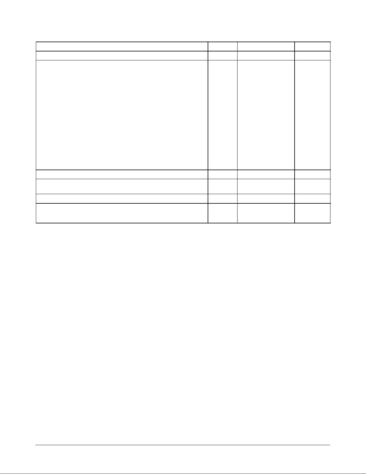
MAXIMUM RATINGS
Rating Symbol Value Unit
Power Supply Input Voltage V
Power Dissipation
Case 369A (DPAK)
TA = 25°C P
Thermal Resistance, Junction−to−Ambient
Thermal Resistance, Junction−to−Case
Case 751 (SOP−8)
TA = 25°C P
Thermal Resistance, Junction−to−Ambient
Thermal Resistance, Junction−to−Case
Case 221A
TA = 25°C P
Thermal Resistance, Junction−to−Ambient
Thermal Resistance, Junction−to−Case
Case 318E
TA = 25°C P
Thermal Resistance, Junction−to−Ambient
Thermal Resistance, Junction−to−Case
Operating Die Junction Temperature Range T
Operating Ambient Temperature Range MC3326
NCV33269
Storage Temperature T
Electrostatic Discharge Sensitivity (ESD)
Human Body Model (HBM)
Machine Model (MM)
JA
JC
JA
JC
JA
JC
JA
JC
T
stg
ESD
in
D
20 V
Internally Limited W
92 °C/W
6.0 °C/W
D
Internally Limited W
160 °C/W
25 °C/W
D
Internally Limited W
65 °C/W
5.0 °C/W
D
Internally Limited W
156 °C/W
15 °C/W
J
A
−40 to +150 °C
−40 to +125
°C
−40 to +125
−55 to +150 °C
V
4000
400
http://onsemi.com
2
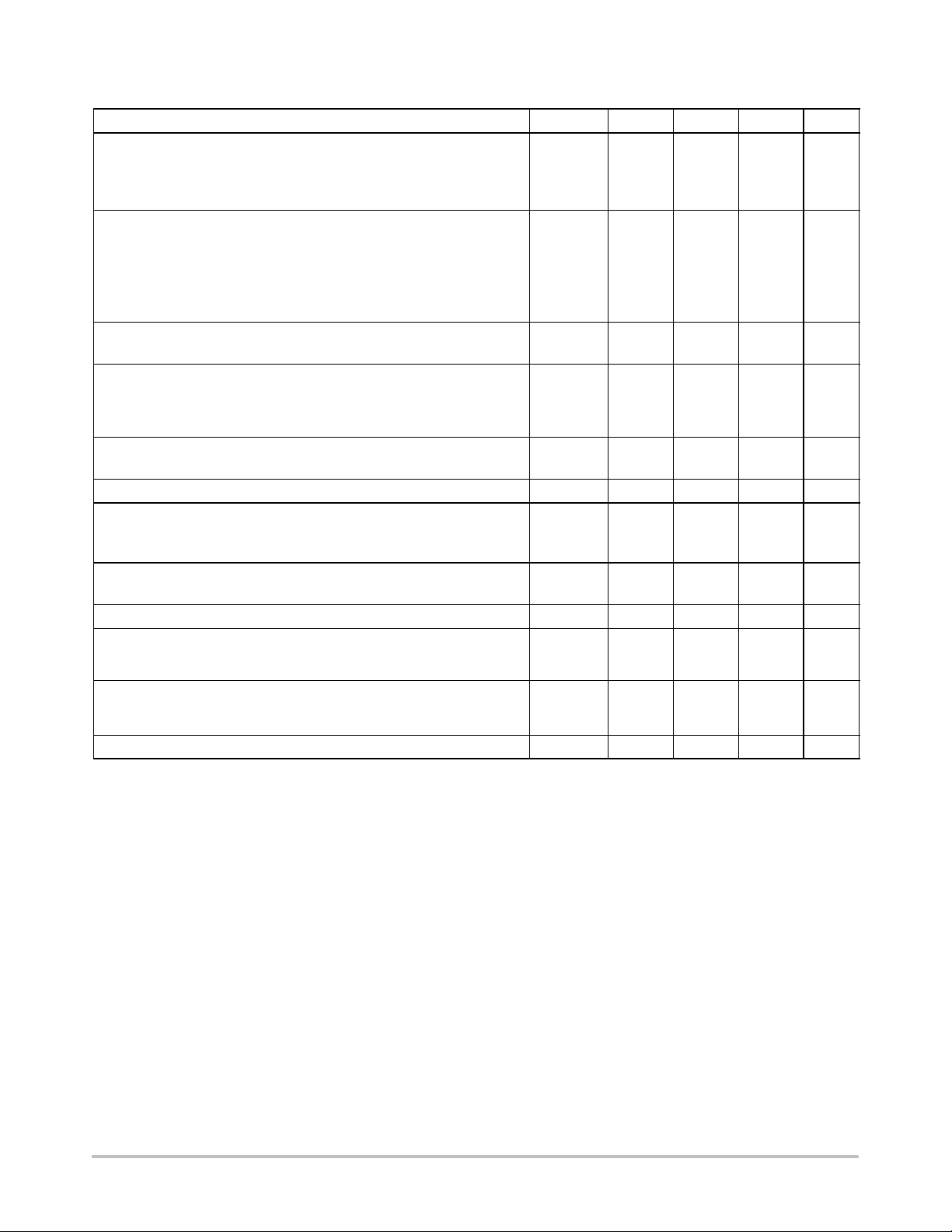
MC33269, NCV33269
ELECTRICAL CHARACTERISTICS (C
= 10 F, TA = 25°C, for min/max values TA = −40°C to +125°C, unless otherwise noted.)
O
Characteristic
Output Voltage (I
3.3 Suffix (V
5.0 Suffix (V
12 Suffix (V
= 10 mA, TA = 25°C)
out
= 5.3 V)
CC
= 7.0 V)
CC
= 14 V)
CC
Output Voltage (Line, Load and Temperature) (Note 1)
(1.25 V ≤ V
(1.35 V ≤ V
in
in
− V
− V
≤ 15 V, I
out
≤ 10 V, I
out
= 500 mA)
out
= 800 mA)
out
3.3 Suffix
5.0 Suffix
12 Suffix
Reference Voltage (I
= 10 mA, Vin − V
out
= 2.0 V, TA = 25°C)
out
for Adjustable Voltage
Reference Voltage (Line, Load and Temperature) (Note 1)
(1.25 V ≤ V
(1.35 V ≤ V
for Adjustable Voltage
in
in
− V
− V
≤ 15 V, I
out
≤ 10 V, I
out
= 500 mA)
out
= 800 mA)
out
Line Regulation
(I
= 10 mA, Vin = [V
out
Load Regulation (Vin = V
+ 1.5 V] to Vin = 20 V, TA = 25°C)
out
+ 3.0 V, I
out
= 10 mA to 800 mA, TA = 25°C) Reg
out
Dropout Voltage
(I
= 500 mA)
out
= 800 mA)
(I
out
Ripple Rejection
(10 V
, 120 Hz Sinewave; I
pp
Current Limit (Vin − V
= 10 V) I
out
= 500 mA)
out
Quiescent Current (Fixed Output)
(1.5 V ≤ V
(5 V ≤ V
out
≤ 12 V)
out
≤ 3.3 V)
Minimum Required Load Current
Fixed Output Voltage
Adjustable Voltage
Adjustment Pin Current I
1. The MC33269−12, Vin − V
is limited to 8.0 V maximum, because of the 20 V maximum rating applied to V
out
Symbol Min Typ Max Unit
V
O
V
O
V
ref
V
ref
Reg
load
Vin−V
line
out
3.27
4.95
11.88
3.23
4.9
11.76
3.3
5.0
12
3.3
5.0
12
3.33
5.05
12.12
3.37
5.1
12.24
1.235 1.25 1.265 V
1.225 1.25 1.275 V
− − 0.3 %
− − 0.5 %
−
−
1.1
1.0
1.25
1.35
RR 55 − − dB
Limit
I
Load
I
Adj
Q
800 − − mA
mA
−
−
5.5
−
20
8.0
mA
−
8.0
−
−
0
−
− − 120 A
in.
V
V
V
http://onsemi.com
3
MC33269, NCV33269
V
in
V
out
Trim Links
V
Adj Gnd
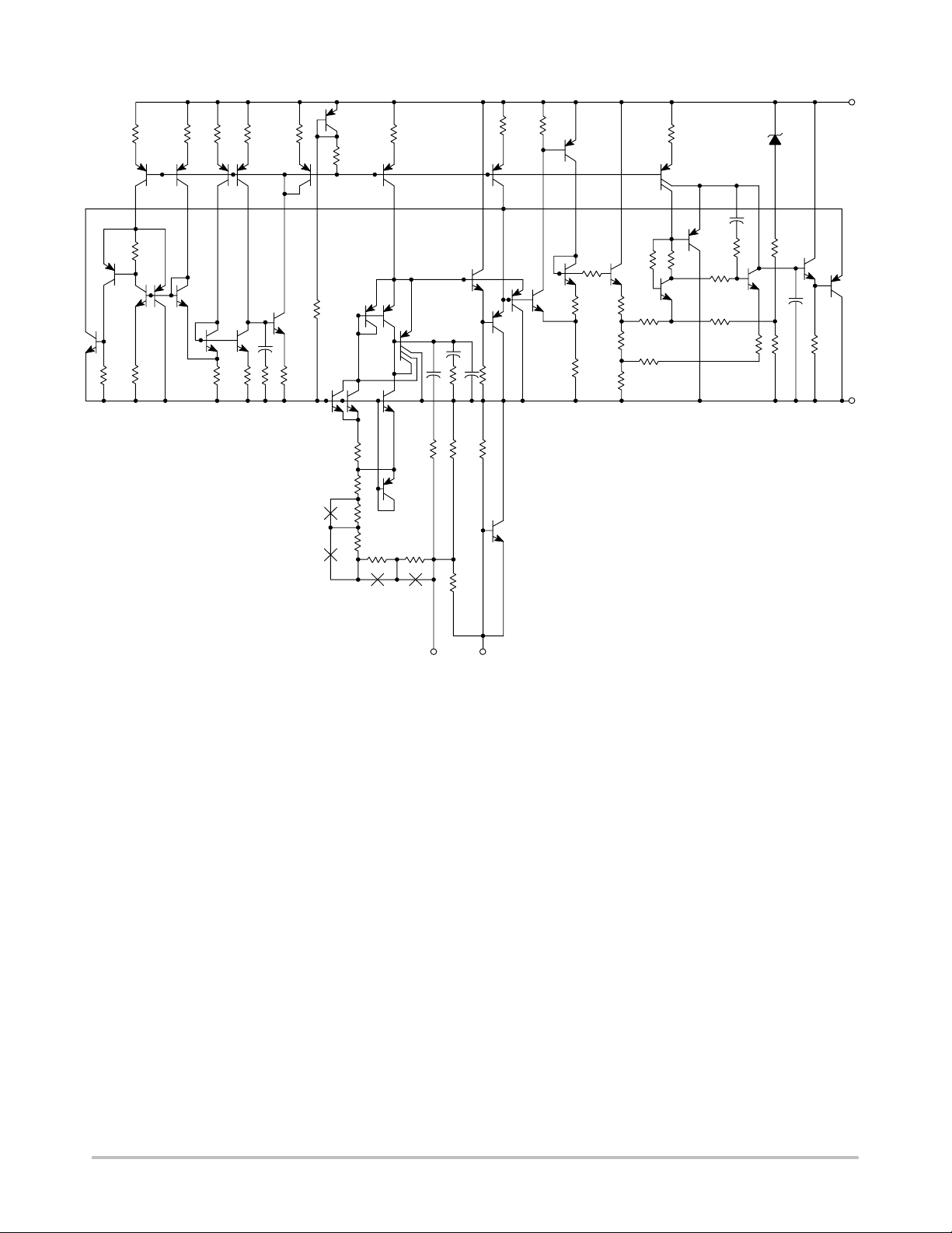
This device contains 38 active transistors.
Figure 1. Internal Schematic
http://onsemi.com
4
1.5
1.3
T
= −40°C
1.1
0.9
T
= 25°C
A
A
T
= 125°C
A
, DROPOUT VOLTAGE (V)
out
0.7
−V
in
V
0.5
0 200 400 600 800 1000
IO, OUTPUT LOAD CURRENT (mA)
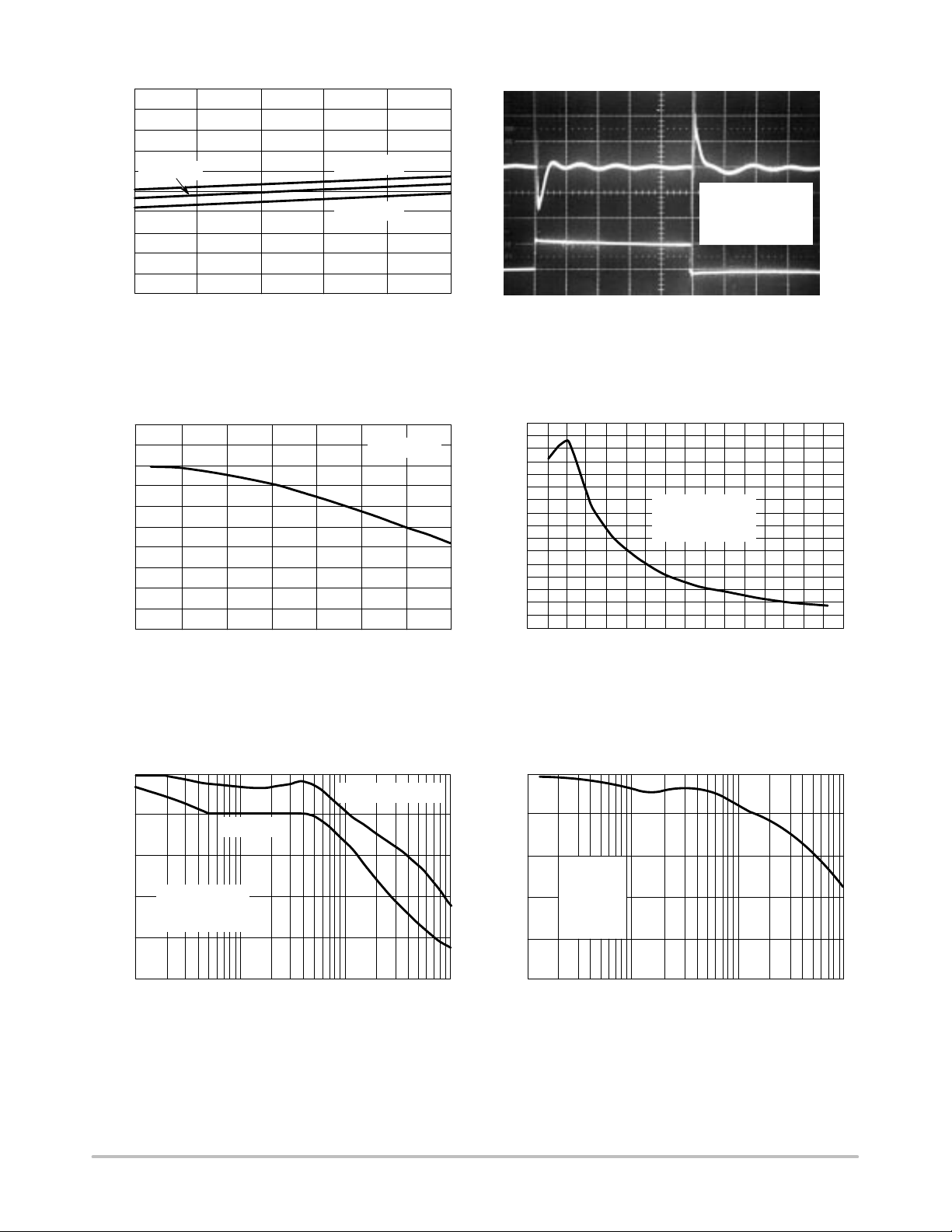
MC33269, NCV33269
, OUTPUT∆
O
V
VOLTAGE DEVIATIONCURRENT
, OUTPUTI
O
20 ms/DIV
C
= 10 F
in
C
= 10 F Tantalum
O
Vin = VO + 3.0 V
Preload = 0.1 A
100
mV/Div
0.5 A
0 A
Figure 2. Dropout Voltage versus
1100
1060
1020
980
940
, OVERVOLTAGE INPUT THRESHOLD (%V )
900
−55
FB(OV) FB
V
70
60
−25 0 25 50 75 100 125
Output Load Current
T
, AMBIENT TEMPERATURE (°C)
A
Figure 4. Dropout Voltage
versus Temperature
VO = 3.3 V or 5.0 V
VO = 12 V
IO = 800 mA
Figure 3. Transient Load Regulation
1.6
1.4
1.2
1.0
0.8
T
= 25°C
A
MC33269D−XX
L = 25 mm Copper
0.6
OUTPUT CURRENT (A)
0.4
0.2
0
0
2.0 4.0 6.0 8.0 10 12 14 16
INPUT−OUTPUT VOLTAGE DIFFERENTIAL (V)
Figure 5. MC33269−XX Output DC Current versus
Input−Output Differential Voltage
70
60
50
Vin = VO + 3.0 V
40
IL = 800 mA
T
= 25°C
A
30
RR, RIPPLE REJECTION RATIO (dB)
20
0.1 1.0 10 100
f, FREQUENCY (kHz)
Figure 6. MC33269 Ripple Rejection
versus Frequency
50
40
30
RR, RIPPLE REJECTION RATIO (dB)
20
0.1
http://onsemi.com
5
Vin = 8.0 V
V
= 5.0 V
out
IL = 800 mA
C
= 22 F
Adj
T
= 25°C
A
f, FREQUENCY (kHz)
Figure 7. MC33269−ADJ Ripple Rejection
versus Frequency
100101.0

MC33269, NCV33269
170
150
P
D(max)
for T
= 50°C
A
130
JUNCTION−TO−AIR ( C/W)°
110
90
Graph represents symmetrical layout
2.0 oz.
L
Copper
70
3.0 mmL
50
R
30
JAθ
R , THERMAL RESISTANCE,
02030504010
JA
L, LENGTH OF COPPER (mm)
Figure 8. SOP−8 Thermal Resistance and Maximum
Power Dissipation versus P.C.B. Copper Length
280
240
200
160
Free Air
Mounted
Vertically
Minimum
Size Pad
3.2
2.8
2.4
2.0
1.6
1.2
0.8
0.4
100
Free Air
90
Mounted
P
D(max)
for T
= 50°C
A
Vertically
80
JUNCTION−TO−AIR ( C/W)°
70
Minimum
Size Pad
60
50
40
010203025155.0
JAθ
R , THERMAL RESISTANCE,
L, LENGTH OF COPPER (mm)
R
JA
Figure 9. DPAK Thermal Resistance and Maximum
Power Dissipation versus P.C.B. Copper Length
P
D(max)
for T
= 50°C
A
2.0 oz. Copper
L
L
2.50
1.25
0.83
0.63
2.0 oz. Copper
L
L
2.4
2.0
1.6
1.2
0.8
0.4
0
120
JAθ
JUNCTION-TO-AIR ( C/W)°
R , THERMAL RESISTANCE
80
40
010203025155.0
R
JA
L, LENGTH OF COPPER (mm)
Figure 10. SOT−223 Thermal Resistance and Maximum
Power Dissipation versus P.C.B. Copper Length
0.50
0.42
0.35
, MAXIMUM POWER DISSIPATION (W)
D
P
http://onsemi.com
6

MC33269, NCV33269
APPLICATIONS INFORMATION
Figures 11 through 15 are typical application circuits. The
output current capability of the regulator is in excess of
800 mA, with a typical dropout voltage of less than 1.0 V.
Internal protective features include current and thermal
limiting.
* The MC33269 requires an external output capacitor for
stability. The capacitor should be at least 10 F with an
equivalent series resistance (ESR) of less than 10 but
greater than 0.2 over the anticipated operating
temperature range. With economical electrolytic capacitors,
cold temperature operation can pose a problem. As
temperature decreases, the capacitance also decreases and
the ESR increases, which could cause the circuit to oscillate.
Also capacitance and ESR of a solid tantalum capacitor is
more stable over temperature. The use of a low ESR ceramic
capacitor placed within close proximity to the output of the
device could cause instability.
** An input bypass capacitor is recommended to improve
transient response or if the regulator is connected to the
V
in
**
C
in
An input capacitor is not necessary for stability, however
it will improve the overall performance.
MC33269−XX
GND
Figure 11. Typical Fixed Output Application
V
in
**
C
in
MC33269
Adj
I
out
1.25
R
S
Figure 13. Current Regulator
V
out
*
C
o
10 F
R
I
S
out
*
C
o
10 F
supply input filter with long wire lengths. This will reduce
the circuit’s sensitivity to the input line impedance at high
frequencies. A 0.33 F or larger tantalum, mylar, ceramic,
or other capacitor having low internal impedance at high
frequencies should be chosen. The bypass capacitor should
be mounted with shortest possible lead or track length
directly across the regulator’s input terminals. Applications
should be tested over all operating conditions to insure
stability.
Internal thermal limiting circuitry is provided to protect
the integrated circuit in the event that the maximum junction
temperature is exceeded. When activated, typically at
170°C, the output is disabled. There is no hysteresis built
into the thermal limiting circuit. As a result, if the device is
overheating, the output will appear to be oscillating. This
feature is provided to prevent catastrophic failures from
accidental device overheating. It is not intended to be used
as a substitute for proper heat−sinking.
R1
R2
Adj
V
out
*
C
o
10 F
R2
V
in
**
C
in
V
is optional, however it will improve the ripple rejection.
***C
Adj
The MC34269 develops a 1.25 V reference voltage between the
output and the adjust terminal. Resistor R1, operates with
constant current to flow through it and resistor R2. This current
should be set such that the Adjust Pin current causes negligible
drop across resistor R2. The total current with minimum load
should be greater than 8.0 mA.
1.25
out
MC33269
Adj
C
Adj
***
R2
1
I
R1
Figure 12. Typical Adjustable Output Application
V
in
**
C
in
**
C
The Schottky diode in series with the ground leg of the upper
regulator shifts its output voltage higher by the forward
voltage drop of the diode. This will cause the lower device
to remain off until the input voltage is removed.
MC33269−XX
GND
MC33269−XX
in
GND
V
out
C
o
10 F
*
Figure 14. Battery Backed−Up Power Supply
http://onsemi.com
V
in
**
C
in
R2 sets the maximum output voltage. Each transistor
reduces the output voltage when turned on.
MC33269
R1
Adj
R2
Figure 15. Digitally Controlled Voltage Regulator
7
V
out
*
C
o
10 F

MC33269, NCV33269
ORDERING INFORMATION
Device Package Shipping Information
MC33269D SO−8 98 Units / Rail
MC33269DR2 SO−8 2500 Units / Tape & Reel
MC33269DR2G SO−8 (Pb−Free) 2500 Units / Tape & Reel
MC33269DT DPAK 75 Units / Rail
MC33269DTG DPAK (Pb−Free) 75 Units / Rail
MC33269DTRK DPAK 2500 Units / Tape & Reel
MC33269DTRKG DPAK (Pb−Free) 2500 Units / Tape & Reel
MC33269T TO−220 50 Units / Rail
MC33269D−3.3 SO−8 98 Units / Rail
MC33269DR2−3.3 SO−8 2500 Units / Tape & Reel
MC33269DR2−3.3G SO−8 (Pb−Free) 2500 Units / Tape & Reel
MC33269DT−3.3 DPAK 75 Units / Rail
MC33269DT−3.3G DPAK (Pb−Free) 75 Units / Rail
MC33269DTRK−3.3 DPAK 2500 Units / Tape & Reel
MC33269DTRK−3.3G DPAK (Pb−Free) 2500 Units / Tape & Reel
MC33269ST−3.3T3 SOT−223 4000 Units / Tape & Reel
MC33269ST−3.3T3G SOT−223 (Pb−Free) 4000 Units / Tape & Reel
MC33269T−3.3 TO−220 50 Units / Rail
MC33269D−5.0 SO−8 98 Units / Rail
MC33269DR2−5.0 SO−8 2500 Units / Tape & Reel
MC33269DT−5.0 DPAK 75 Units / Rail
MC33269DTRK−5.0 DPAK 2500 Units / Tape & Reel
MC33269DTRK−5.0G DPAK (Pb−Free) 2500 Units / Tape & Reel
MC33269T−5.0 TO−220 50 Units / Rail
MC33269D−12 SO−8 98 Units / Rail
MC33269DR2−12 SO−8 2500 Units / Tape & Reel
MC33269DT−12 DPAK 75 Units / Rail
MC33269DTRK−12 DPAK 2500 Units / Tape & Reel
MC33269DTRK−12G DPAK (Pb−Free) 2500 Units / Tape & Reel
MC33269T−12 TO−220 50 Units / Rail
NCV33269DTRK* DPAK 2500 Units / Tape & Reel
NCV33269DTRK−3.3* DPAK 2500 Units / Tape & Reel
NCV33269DTRK−12* DPAK 250 Units / Tape & Reel
†For information on tape and reel specifications, including part orientation and tape sizes, please refer to our Tape and Reel Packaging
Specifications Brochure, BRD8011/D.
*NCV prefix is for automotive and other applications requiring site and control changes.
†
http://onsemi.com
8

MC33269, NCV33269
MARKING DIAGRAMS
SO−8
D SUFFIX
CASE 751
8
8
8
8
269AJ
ALYWW
123
269AJ
ALYW
1
69−12
ALYWW
123
69−12
ALYW
1
DPAK
DT SUFFIX
CASE 369A
269−3
ALYWW
123
TO−220AB
T SUFFIX
CASE 221A
269−3
ALYW
1
269−5
ALYWW
123
269−5
ALYW
1
SOT−223
ST SUFFIX
CASE 318E
ALYW
2693
123
MC
33269T
AWLYWW
23 1
1
MC
33269T−12
AWLYWW
23 1
A = Assembly Location
WL, L = Wafer Lot
Y = Year
WW, W = Work Week
33269T−3.3
AWLYWW
MC
33269T−5.0
AWLYWW
23 1
MC
23
http://onsemi.com
9

−Y−
−Z−
MC33269, NCV33269
PACKAGE DIMENSIONS
SO−8
D SUFFIX
CASE 751−07
ISSUE AA
−X−
B
H
A
58
1
4
G
D
0.25 (0.010) Z
M
S
Y
0.25 (0.010)
C
SEATING
PLANE
SXS
M
0.10 (0.004)
M
Y
K
N
X 45
M
NOTES:
1. DIMENSIONING AND TOLERANCING PER ANSI
Y14.5M, 1982.
2. CONTROLLING DIMENSION: MILLIMETER.
3. DIMENSION A AND B DO NOT INCLUDE MOLD
PROTRUSION.
4. MAXIMUM MOLD PROTRUSION 0.15 (0.006) PER
SIDE.
5. DIMENSION D DOES NOT INCLUDE DAMBAR
PROTRUSION. ALLOWABLE DAMBAR
PROTRUSION SHALL BE 0.127 (0.005) TOTAL IN
EXCESS OF THE D DIMENSION AT MAXIMUM
MATERIAL CONDITION.
6. 751−01 THRU 751−06 ARE OBSOLETE. NEW
STANDARD IS 751−07.
MILLIMETERS
DIMAMIN MAX MIN MAX
4.80 5.00 0.189 0.197
B 3.80 4.00 0.150 0.157
C 1.35 1.75 0.053 0.069
D 0.33 0.51 0.013 0.020
G 1.27 BSC 0.050 BSC
H 0.10 0.25 0.004 0.010
J
J 0.19 0.25 0.007 0.010
K 0.40 1.27 0.016 0.050
M 0 8 0 8
N 0.25 0.50 0.010 0.020
S 5.80 6.20 0.228 0.244
INCHES
SOLDERING FOOTPRINT*
1.52
0.060
7.0
0.275
0.6
0.024
4.0
0.155
1.270
0.050
SCALE 6:1
inches
mm
Figure 16. SO−8
*For additional information on our Pb−Free strategy and soldering
details, please download the ON Semiconductor Soldering and
Mounting Techniques Reference Manual, SOLDERRM/D.
http://onsemi.com
10

MC33269, NCV33269
DPAK
DT SUFFIX
CASE 369A−13
ISSUE AB
NOTES:
SEATING
−T−
PLANE
B
V
S
R
4
A
123
K
F
L
D
2 PL
G
0.13 (0.005) T
C
E
Z
U
J
H
M
1. DIMENSIONING AND TOLERANCING PER ANSI
Y14.5M, 1982.
2. CONTROLLING DIMENSION: INCH.
DIM MIN MAX MIN MAX
A 0.235 0.250 5.97 6.35
B 0.250 0.265 6.35 6.73
C 0.086 0.094 2.19 2.38
D 0.027 0.035 0.69 0.88
E 0.033 0.040 0.84 1.01
F 0.037 0.047 0.94 1.19
G 0.180 BSC 4.58 BSC
H 0.034 0.040 0.87 1.01
J 0.018 0.023 0.46 0.58
K 0.102 0.114 2.60 2.89
L 0.090 BSC 2.29 BSC
R 0.175 0.215 4.45 5.46
S 0.020 0.050 0.51 1.27
U 0.020 −−− 0.51 −−−
V 0.030 0.050 0.77 1.27
Z 0.138 −−− 3.51 −−−
MILLIMETERSINCHES
SOLDERING FOOTPRINT*
6.20
0.244
2.58
0.101
5.80
0.228
3.0
0.118
0.063
1.6
SCALE 3:1
6.172
0.243
inches
mm
Figure 17. DPAK
*For additional information on our Pb−Free strategy and soldering
details, please download the ON Semiconductor Soldering and
Mounting Techniques Reference Manual, SOLDERRM/D.
http://onsemi.com
11

0.08 (0003)
S
L
H
A
F
4
123
G
MC33269, NCV33269
PACKAGE DIMENSIONS
SOT−223
ST SUFFIX
CASE 318E−04
ISSUE K
B
D
C
M
SOLDERING FOOTPRINT*
NOTES:
1. DIMENSIONING AND TOLERANCING PER ANSI
Y14.5M, 1982.
2. CONTROLLING DIMENSION: INCH.
INCHES
DIMAMIN MAX MIN MAX
0.249 0.263 6.30 6.70
B 0.130 0.145 3.30 3.70
C 0.060 0.068 1.50 1.75
D 0.024 0.035 0.60 0.89
F 0.115 0.126 2.90 3.20
G 0.087 0.094 2.20 2.40
H 0.0008 0.0040 0.020 0.100
J
J 0.009 0.014 0.24 0.35
K 0.060 0.078 1.50 2.00
L 0.033 0.041 0.85 1.05
M 0 10 0 10
S 0.264 0.287 6.70 7.30
MILLIMETERS
K
3.8
0.15
2.0
0.079
2.3
0.091
2.3
0.091
6.3
0.248
2.0
0.079
mm
1.5
0.059
SCALE 6:1
inches
Figure 18. SOT−223
*For additional information on our Pb−Free strategy and soldering
details, please download the ON Semiconductor Soldering and
Mounting Techniques Reference Manual, SOLDERRM/D.
http://onsemi.com
12

MC33269, NCV33269
TO−220AB
T SUFFIX
CASE 221A−09
ISSUE AA
SEATING
−T−
PLANE
B
4
Q
123
F
T
A
U
C
S
H
K
Z
L
V
R
J
G
D
N
NOTES:
1. DIMENSIONING AND TOLERANCING PER ANSI
Y14.5M, 1982.
2. CONTROLLING DIMENSION: INCH.
3. DIMENSION Z DEFINES A ZONE WHERE ALL
BODY AND LEAD IRREGULARITIES ARE
ALLOWED.
DIM MIN MAX MIN MAX
A 0.570 0.620 14.48 15.75
B 0.380 0.405 9.66 10.28
C 0.160 0.190 4.07 4.82
D 0.025 0.035 0.64 0.88
F 0.142 0.147 3.61 3.73
G 0.095 0.105 2.42 2.66
H 0.110 0.155 2.80 3.93
J 0.018 0.025 0.46 0.64
K 0.500 0.562 12.70 14.27
L 0.045 0.060 1.15 1.52
N 0.190 0.210 4.83 5.33
Q 0.100 0.120 2.54 3.04
R 0.080 0.110 2.04 2.79
S 0.045 0.055 1.15 1.39
T 0.235 0.255 5.97 6.47
U 0.000 0.050 0.00 1.27
V 0.045 −−− 1.15 −−−
Z −−− 0.080 −−− 2.04
MILLIMETERSINCHES
http://onsemi.com
13

MC33269, NCV33269
ON Semiconductor and are registered trademarks of Semiconductor Components Industries, LLC (SCILLC). SCILLC reserves the right to make changes without further notice
to any products herein. SCILLC makes no warranty, representation or guarantee regarding the suitability of its products for any particular purpose, nor does SCILLC assume any liability
arising out of the application or use of any product or circuit, and specifically disclaims any and all liability, including without limitation special, consequential or incidental damages.
“Typical” parameters which may be provided in SCILLC data sheets and/or specifications can and do vary in different applications and actual performance may vary over time. All
operating parameters, including “Typicals” must be validated for each customer application by customer’s technical experts. SCILLC does not convey any license under its patent rights
nor the rights of others. SCILLC products are not designed, intended, or authorized for use as components in systems intended for surgical implant into the body, or other applications
intended to support or sustain life, or for any other application in which the failure of the SCILLC product could create a situation where personal injury or death may occur. Should
Buyer purchase or use SCILLC products for any such unintended or unauthorized application, Buyer shall indemnify and hold SCILLC and its officers, employees, subsidiaries, affiliates,
and distributors harmless against all claims, costs, damages, and expenses, and reasonable attorney fees arising out of, directly or indirectly, any claim of personal injury or death
associated with such unintended or unauthorized use, even if such claim alleges that SCILLC was negligent regarding the design or manufacture of the part. SCILLC is an Equal
Opportunity/Affirmative Action Employer. This literature is subject to all applicable copyright laws and is not for resale in any manner.
PUBLICATION ORDERING INFORMATION
LITERATURE FULFILLMENT:
Literature Distribution Center for ON Semiconductor
P.O. Box 5163, Denver, Colorado 80217 USA
Phone: 303−675−2175 or 800−344−3860 Toll Free USA/Canada
Fax: 303−675−2176 or 800−344−3867 Toll Free USA/Canada
Email: orderlit@onsemi.com
N. American Technical Support: 800−282−9855 Toll Free
USA/Canada
Japan: ON Semiconductor, Japan Customer Focus Center
2−9−1 Kamimeguro, Meguro−ku, Tokyo, Japan 153−0051
Phone: 81−3−5773−3850
http://onsemi.com
ON Semiconductor Website: http://onsemi.com
Order Literature: http://www.onsemi.com/litorder
For additional information, please contact your
local Sales Representative.
MC33269/D
14
 Loading...