

ON Semiconductor ASP0800 Datasheet
Programmable Multi-Phase Synchronous
Buck Converter with PMBus
Preliminary Technical Data
ASP0800
ERY FEATURES
Selectable 1-, 2-, 3-, 4-, 5-, 6, 7 or 8- phase operation at up to
1 MHz per phase
PMBus Interface - enables digital programmability of set
points and readback of monitored values
Logic-level PWM outputs for interface to external high
power drivers
Fast-Enhanced PWM flex mode for excellent load transient
performance
Active current balancing between all output phases
Built-in power-good/crowbar blanking supports on-the-fly
VID code changes
Digitally programmable 0.375 V to 1.6 V output supports
both VR11 and VR11.1 specifications
Programmable Offset up to ±200mV
Programmable short-circuit protection with programmable
latch-off delay
Supports PSI# – Power saving mode during light loads
Over – Clocking Control
APPLICATIONS
CPU Power controllers for Servers, Workstations and high
end Desktops.
Next generation Intel® VRM modules
POL Applications such as Memory
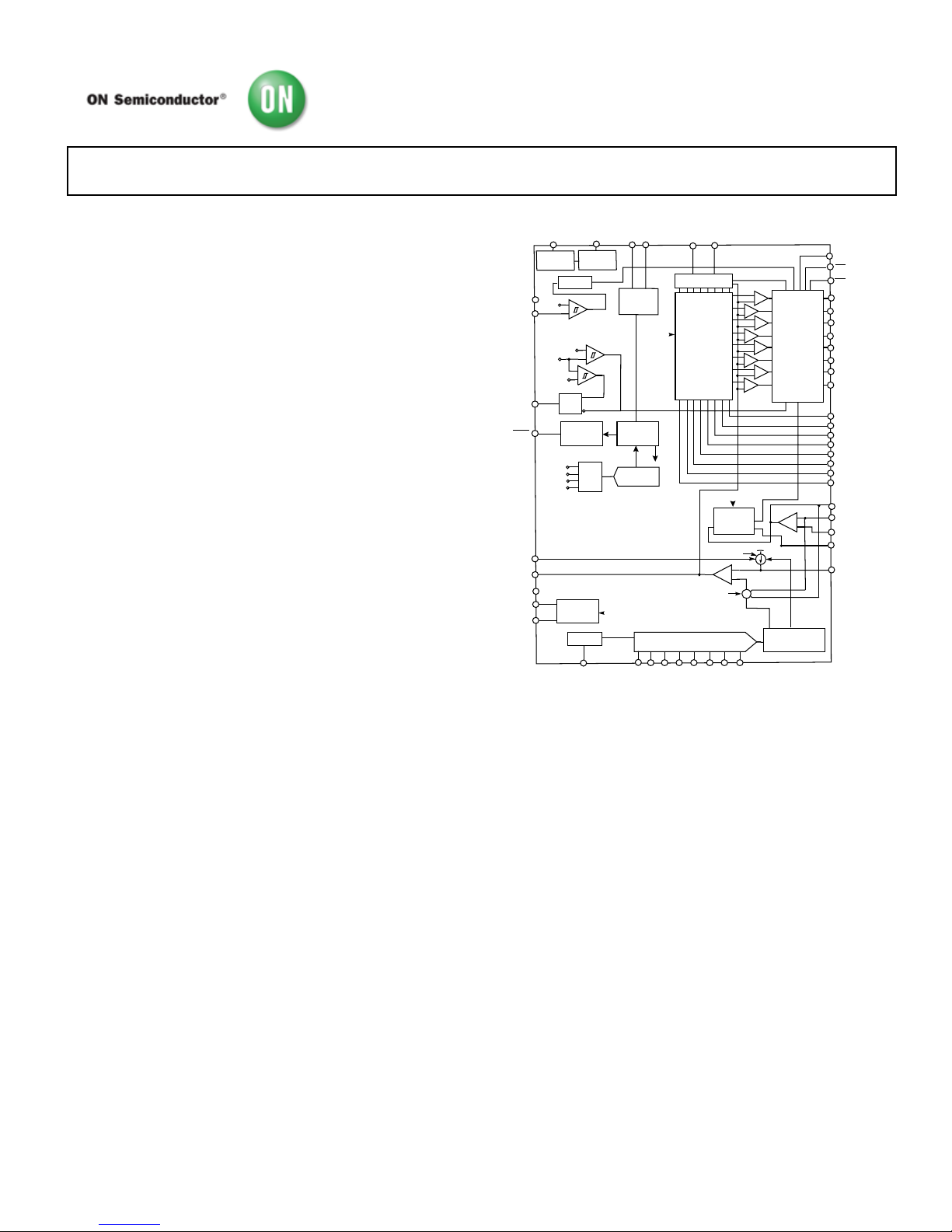
FUNCTIONAL BLOCK DIAGRAM
VCC
PRECISION
REFERENCE
DEL AY
–
+
GND
ASP0800
EN/VTT
13
PWRGD
6
RAMPADJ
18
RT
17
28
SW3
PWM2
37
CSREF
7
CSCOMP
PWM3
36
PWM4
35
CSSUM
22
FB
19
PWM1
VID2VID1 VID3 VID4 VID5 VID7VID6
2
COMP
FBRTN
VID DAC
CURRENT
MEASUREMENT
AND LIMIT
CROWBAR
CURRENT
LIMIT
+
–
40444546
47
OD1
SW2
29
SW4
27
12
16
+
–
OSCILLATOR
–
+
SW1
30
38
4143 42
11
IREF
VID0
10
IMON
CONTROL
CONTROL
CONTROL
CONTROL
CONTROL
ADC
PSI#
39
14
48
SMBUS
SCL
SD
A
5
4
BOOT VOLTAGE&
SOFT START CONTROL
ILIMITFS
20
1
VCC3
CONTROL
–
+
850mV
–
+
CONTROL
+
–
CSREF
UVLO
SHUTDOWN
SHUNT
REGULATOR
3.3V
REGULATOR
CLOCK
CONTROL
OC1
OC2
CONTROL
9
8
15
21
ODN
DIG ITAL
REGISTERS
24
SW7
SW6
25
SW8
23
SW5
26
+
–
CMP
PWM6
33
PWM7
32
PWM8
31
+
–
CMP
+
–
CMP
+
–
CMP
+
–
CMP
+
–
CMP
+
–
CMP
+
–
CMP
PWM5
34
CURRENT
BALANCING
CIRCUIT
1- 8 PHASE
DRIVER LOGIC
EN
SET
RESET
RESET
RESET
RESET
RESET
RESET
RESET
RESET
EN
FB
FBRTN
IMON
MUX
ALERT
3
COMPARATORS
Figure 1. Functional Block Diagram
GENERAL DESCRIPTION
The ASP08001 is an integrated power control IC with a PMBus
interface. The ASP0800 is a highly efficient, multiphase,
synchronous buck switching regulator controller, which aids
design of High Efficiency and High Density solutions.
The PMBus interface enables digital programming of key
system parameters to optimize system performance and provide
feedback to the system. The ASP0800 is compatible for use with
coupled inductors,
The ASP0800 is optimized for converting a 12 V main supply
into the core supply voltage required by high performance Intel
processors. It uses an internal 8-bit DAC to read the voltage
identification (VID) code directly from the processor, which is
used to set the output voltage between 0.375 V and 1.6 V.
This device uses a multimode PWM architecture to drive the
logic-level outputs at a programmable switching frequency that
can be optimized for VR size and efficiency. The ASP0800 can
be programmed for 1-, 2-, 3-, 4-, 5-, 6, 7 or 8- phase operation,
allowing for the construction of up to 8 complementary buck
switching stages. The ASP0800 support PSI#, which is a power
phases at light loads.
The ASP0800 includes a PMBus interface, which can be used to
program system set points such as voltage offset, load line,
phase balance and output voltage. Key system performance data
such as CPU current, CPU voltage, and power and fault
conditions can also be read back over the PMBus from the
ASP0800.
The ASP0800 OC Feature allows programming different offset
voltages depending on the load current being supplied. 3 OC
Thresholds and 4 OC Offsets value registers are supported.
The ASP0800 has a built in shunt regulator that allows the part
to be powered from the +12V system supply through a series
resistor. The ASP0800 is specified over the extended
commercial temperature range of 0°C to +85°C and is available
in a 48 Lead LFCSP package.
1
Protected by U.S. Patent Number 6,683,441; other patents pending.
Downloaded from DatasheetLib.com - datasheet search engine Downloaded from DatasheetLib.com - datasheet search engine
©2008 SCILLC. All rights reserved. Publication Order Number:
March 2008 - Rev. P1 ASP0800/S

ASP0800 Preliminary Technical Data
TABLE OF CONTENTS
Features.............................................................................................. 1
Applications....................................................................................... 1
Functional Block Diagram .............................................................. 1
General Description ......................................................................... 1
Specifications..................................................................................... 3
Test Circuits....................................................................................... 6
Absolute Maximum Ratings............................................................ 7
Thermal Resistance ...................................................................... 7
ESD Caution.................................................................................. 7
Pin Configuration and Function Descriptions............................. 8
Typical Performance Characteristics ........................................... 10
Theory of Operation ...................................................................... 11
Start-Up Sequence...................................................................... 11
Phase Detection Sequence......................................................... 11
Master Clock Frequency............................................................ 12
Output Voltage Differential Sensing ........................................ 12
Output Current Sensing ............................................................ 12
Output current monitor ............................................................ 12
Dynamic VID ............................................................................. 13
INTERNAL Delay Timer .......................................................... 14
Soft Start ...................................................................................... 14
Current-Limit, Short-Circuit, and Latch-Off Protection...... 16
Power-Good Monitoring........................................................... 17
POWER STATE INDICATOR ................................................. 17
Output Crowbar......................................................................... 18
Output Enable and UVLO........................................................ 18
OVERCLOCKING (OC) LIMITS AND OFFSETS .............. 18
PMBUS Interface........................................................................ 18
Write Operations........................................................................ 21
Read Operations......................................................................... 22
PMBus Timeout.......................................................................... 23
Outline Dimensions....................................................................... 38
03/08—Rev P1: Conversion to ON Semiconductor
REVISION HISTORY
Downloaded from DatasheetLib.com - datasheet search engine Downloaded from DatasheetLib.com - datasheet search engine
Rev. P1 | Page 2 of 36 | www.onsemi.com

Preliminary Technical Data ASP0800
SPECIFICATIONS
VCC = 5 V, FBRTN = GND, TA = 0°C to 85°C, unless otherwise noted.1
Table 1
Parameter Symbol Conditions Min Typ Max Unit
REFERENCE CURRENT
Reference Bias Voltage V
IREF
1.75 1.8 1.85 V
Reference Bias Current I
IREF
R
IREF
= 121 kΩ 15 uA
ERROR AMPLIFIER
Output Voltage Range2 V
COMP
0 4.4 V
Accuracy VFB
Relative to nominal DAC output,
referenced to FBRTN (see Figure 3)
−10 +10 mV
V
FB(BOOT)
In startup 1.09 1.1 1.11 V
Load Line Positioning Accuracy −77 −80 −83 mV
Load Line Range −350 0 mV
Load Line Attenuation 0 100 %
Differential Nonlinearity −1 +1 LSB
Input Bias Current IFB I
FB = IIREF
13.5 15 16.5 µA
Offset Accuracy VR Offset Register = TBD, VID = 1.0V −200 mV
VR Offset Register = TBD , VID = 1.0V 200 mV
FBRTN Current I
FBRTN
70 200 µA
Output Current I
COMP
FB forced to V
OUT
– 3% 500 µA
Gain Bandwidth Product GBW
(ERR)
COMP = FB 20 MHz
Slew Rate COMP = FB 25 V/µs
BOOT Voltage Hold Time t
BOOT
Internal Timer 2 ms
VID INPUTS
Input Low Voltage V
IL(VID)
VID(X) 0.3 V
Input High Voltage V
IH(VID)
VID(X) 0.8 V
Input Current I
IN(VID)
−5 µA
VID Transition Delay Time2 VID code change to FB change 400 ns
No CPU Detection Turn-Off
Delay Time
2
VID code change to PWM going low 5 µs
OSCILLATOR
Frequency Range2 f
OSC
0.25 9 MHz
Frequency Variation f
PHASE
T
A
= 25°C, RT = 500 kΩ, 4-phase 170 195 225 kHz
T
A
= 25°C, RT = 250 kΩ, 4-phase 375 kHz
T
A
= 25°C, RT = 121 kΩ, 4-phase 750 kHz
Output Voltage VRT R
T
= 500 kΩ to GND 1.9 2.0 2.1 V
RAMPADJ Output Voltage V
RAMPADJ
RAMPADJ − FB, VFB = 1V, −50 +50 mV
RAMPADJ Input Current Range I
RAMPADJ
5 125 µA
CURRENT SENSE AMPLIFIER
Offset Voltage V
OS(CSA)
CSSUM − CSREF (see Figure 3) −1.0 +1.0 mV
Input Bias Current, CSREF I
BIAS(CSREF)
CSREF = 1V −20 +20 µA
Input Bias Current, CSSUM I
BIAS(CSSUM)
CSREF = 1V −10 +10 nA
Gain Bandwidth Product GBW
(CSA)
CSSUM = CSCOMP 10 MHz
Slew Rate C
CSCOMP
= 10 pF 10 V/µs
Input Common-Mode Range CSSUM and CSREF 0 3.0 V
Output Voltage Range 0.05 3.0 V
Output Current I
CSCOMP
500 µA
Current Limit Latch off Delay Time Internal Timer 8 ms
1
All limits at temperature extremes are guaranteed via correlation using standard statistical quality control (SQC).
2
Guaranteed by design or bench characterization, not tested in production.
Downloaded from DatasheetLib.com - datasheet search engine Downloaded from DatasheetLib.com - datasheet search engine
Rev. P1 | Page 3 of 36 | www.onsemi.com

ASP0800 Preliminary Technical Data
Parameter Symbol Conditions Min Typ Max Unit
PSI#
Input Low Voltage 0.3 V
Input High Voltage 0.8 V
Input Current −5 µA
Assertion Timing Fsw = 300kHz 3.3 µs
Deassertion Timing Fsw = 300kHz 825 ns
IMON OUTPUT
Clamp Voltage 1.0 1.15 V
Accuracy
10 × (CSREF − CSCOMP)/RILIM
−3 3 %
Output Current
800 µA
Offset
−3 3 mV
CURRENT LIMIT COMPARITOR
ILIM Bias Current I
LIM
CSREF − CSCOMP)/RILIM , (CSREF −
CSCOMP)=150 mV, RI
LIMC=7.5 kΩ
20 µA
Current Limit Threshold Current ICL
4/3 × IIREF
20 µA
CURRENT BALANCE AMPLIFIER
Common-Mode Range V
SW(X)CM
−600 +200 mV
Input Resistance R
SW(X)
SW(X) = 0 V 14 19 25 kΩ
Input Current I
SW(X)
SW(X) = 0 V 7 12 20 µA
Input Current Matching
'I
SW(X)
SW(X) = 0 V −6 +6 %
Phase Balance Adjustment Range Low Phase Bal Registers = 00000 -25 %
Phase Balance Adjustment Range
High
Phase Bal Registers = 11111 +25 %
DELAY TIMER
Internal Timer Delay Time Register = 011 2 ms
Timer Range Low Delay Time Register = 000 0.5 ms
Timer Range High Delay Time Register = 111 4 ms
SOFT START
Internal Timer Soft Start Slope Register = 010 0.5 V/ms
Timer Range Low Soft Start Slope Register = 000 0.1 V/ms
Timer Range High Soft Start Slope Register = 111 1.5 V/ms
ENABLE INPUT
Input Low Voltage V
IL(EN)
0.3 V
Input High Voltage V
IH(EN)
0.8 V
Input Current I
IN(EN)
−1 µA
Delay Time t
DELAY(EN)
EN > 0.8V , Internal Delay 2 ms
ODN / OD1 OUTPUTS
Output Low Voltage V
OL(
ODN/1
, )
I
OD(SINK)
= −400 PA
160 500 mV
Output High Voltage V
OH(
ODN/1
)
I
OD(SOURCE)
= 400 PA
4 5 V
ODN / OD1 Pull-Down Resistor
60 kΩ
OVER-CLOCKING OUTPUTS (OC1, OC2)
Output Low Voltage VOL I
OC(SINK)
= -1 mA 160 500 mV
POWER GOOD COMPARATOR
Undervoltage Threshold V
PWRGD(UV)
Relative to nominal DAC output −600 −500 −400 mV
Undervoltage Adjustment Range Low PWRGD_LO Register = 000 −500 mV
Undervoltage Adjustment Range
High
PWRGD_LO Register = 111 −150 mV
Overvoltage Threshold V
PWRGD(OV)
Relative to DAC output, PWRGD_Hi = 00 200 300 400 mV
Overvoltage Adjustment Range Low PWRGD_Hi Register = 11 150 mV
Overvoltage Adjustment Range High PWRGD_Hi Register = 00 300 mV
Output Low Voltage V
OL(PWRGD)
I
PWRGD(SINK)
= −4 mA 150 300 mV
Power Good Delay Time
Downloaded from DatasheetLib.com - datasheet search engine Downloaded from DatasheetLib.com - datasheet search engine
Rev. P1 | Page 4 of 36 | www.onsemi.com

Preliminary Technical Data ASP0800
Rev. Pr H| Page 5 of 38
Parameter Symbol Conditions Min Typ Max Unit
During Soft Start2 Internal Timer 2 ms
VID Code Changing 100 250 µs
VID Code Static 200 ns
Crowbar Trip Point V
CROWBAR
Relative to DAC output, PWRGD_Hi = 00 200 300 400 mV
Overvoltage Adjustment Range Low PWRGD_Hi Register = 11 150 mV
Overvoltage Adjustment Range High PWRGD_Hi Register = 00 300 mV
Crowbar Reset Point Relative to FBRTN 250 300 350 mV
Crowbar Delay Time t
CROWBAR
Overvoltage to PWM going low
VID Code Changing 100 250 µs
VID Code Static 400 ns
PWM OUTPUTS
Output Low Voltage V
OL(PWM)
I
PWM(SINK)
= −400 µA 160 500 mV
Output High Voltage V
OH(PWM)
I
PWM(SOURCE)
= 400 µA 4 5 V
PMBus Interface
Logic High Input Voltage V
IH(SDA, SCL)
2.1 V
Logic Input Low Voltage V
IL(SDA, SCL)
0.8 V
Hysteresis 500 mV
SDA Output Low Voltage VOL I
SDA
= −6mA 0.4 V
Input Current I
IH
; IIL −1 1 µA
Input Capacitance C
SCL, SDA
5 pF
Clock Frequency f
SCL
400 kHz
SCL Falling Edge to SDA Valid Time 1 µs
ALERT
FAU LT
OUTPUTS
Output Low Voltage VOL I
OUT
= -6mA 0.4 V
Output High Leakage Current IOH V
OH
= 5V 1 uA
ANALOG/DIGITAL CONVERTER
Total Unadjusted Error (TUE) ±2 %
Differential Non linearity (DNL) TBD Bits 1 LSB
Conversion Time Averaging Enabled (32 averages) 80 ms
SUPPLY V
SYSTEM
= 12 V, R
SHUNT
= 340 Ω
VCC2 VCC 4.70 5 5.45 V
DC Supply Current I
VCC
V
SYSTEM
= 13.2 V, R
SHUNT
= 340 Ω 21 26 mA
UVLO Turn-On Current 6.5 11 mA
UVLO Threshold Voltage V
UVLO
VCC rising 9 V
UVLO Turn-Off Voltage VCC falling 4.1 V
VCC3 Output Voltage VCC3 I
VCC3
= 1mA 3.0 3.3 3.6 V
Downloaded from DatasheetLib.com - datasheet search engine Downloaded from DatasheetLib.com - datasheet search engine
Rev. P1 | Page 5 of 36 | www.onsemi.com
ASP0800 Preliminary Technical Data
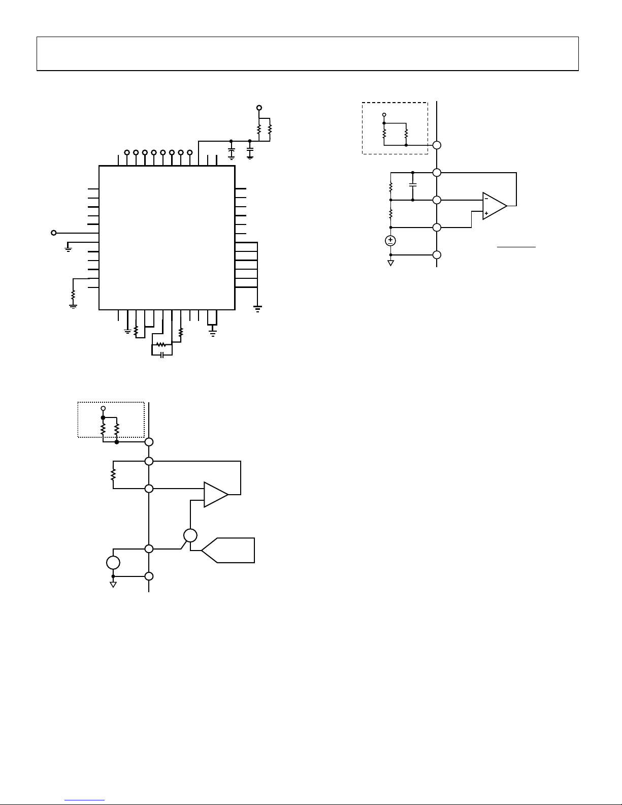
TEST CIRCUITS
VCC3
PWRGD
ALERT
SDA
SCL
EN
GND
OC1
OC2
IMON
IREF
RT
RAMPADJ
FBRTN
COMPFBCSREF
CSSUM
CSCOMP
ILIMITFS
ODN
OD1
SW8
SW7
PWM3
PWM4
PWM5
PWM6
PWM7
PWM8
SW1
SW2
SW3
SW4
SW5
SW6
PSI
VID0
VID1
VID2
VID3
VID4
VID5
VID6
VID7
VCC
PWM1
PWM2
ASP0800
8 BIT
VID CODE
100nF
+12V
680
:
680
:
1
µF
+
121k:
10k:
20k:
100nF
1k:
+1.25V
Figure 2. Closed-Loop Output Voltage Accuracy
+
–
39
VCC
CSREF
GND
7
FB
15
COMP
16
10k
A
SP0800
+
–
+
'VFB = FB'V=80mV - F B'V=0mV
VID
DAC
1.0V
+
–
+12V
680:
680:
17
Figure 3 . Current Sense Amplifier V
OS
CSSUM
19
CSCOMP
18
39
VCC
CSREF
17
GND
7
39k
680 680
100nF
1k
1V
ASP0800
VOS =
CSCOMP – 1V
40
12V
Figure 4 . Positioning Voltage
Downloaded from DatasheetLib.com - datasheet search engine Downloaded from DatasheetLib.com - datasheet search engine
Rev. P1 | Page 6 of 36 | www.onsemi.com
Preliminary Technical Data ASP0800
Rev. Pr H| Page 7 of 38
ABSOLUTE MAXIMUM RATINGS
Table 2.
Parameter Rating
VCC −0.3 V to +6 V
FBRTN −0.3 V to +0.3 V
PWM2 to PWM8, RAMPADJ −0.3 V to VCC + 0.3 V
SW1 to SW8 −5 V to +25 V
<200 ns −10 V to +25 V
All Other Inputs and Outputs −0.3 V to VCC + 0.3 V
Storage Temperature Range −65°C to +150°C
Operating Ambient Temperature Range 0°C to 85°C
Operating Junction Temperature 125°C
Lead Temperature
Soldering (10 sec)
300°C
Infrared (15 sec) 260°C
Stresses above those listed under Absolute Maximum Ratings
may cause permanent damage to the device. This is a stress
rating only; functional operation of the device at these or any
other conditions above those indicated in the operational
section of this specification is not implied. Exposure to absolute
maximum rating conditions for extended periods may affect
device reliability.
THERMAL RESISTANCE
θJA is specified for the worst-case conditions, that is, a device
soldered in a circuit board for surface-mount packages.
Table 3. Thermal Resistance
Package Type θJA θ
JC
Unit
Thermal Impedance (θJA) 27°C/W
ESD CAUTION
Downloaded from DatasheetLib.com - datasheet search engine Downloaded from DatasheetLib.com - datasheet search engine
Rev. P1 | Page 7 of 36 | www.onsemi.com
ASP0800 Preliminary Technical Data
PIN CONFIGURATION AND FUNCTION DESCRIPTIONS
13141516171819
2021222324
FBRTN
COMP
FB
CSREF
CSSUM
CSCOMP
ILIMFS
ODN
OD1
SW8
SW7
RAMPADJ
4847464544434241403938
37
PSI
VID0
VID1
VID2
VID3
VID4
VID5
VID6
PWM1
PWM2
1
2
3
4
5
6
7
8
9
10
11
12
VCC3
PWRGD
ALERT
SDA
SCL
EN
GND
OC1
OC2
IMON
IREF
RT
PWM4
PWM5
PWM6
PWM7
PWM8
SW1
SW2
SW3
SW4
SW5
SW6
35
PWM336
34
33
32
31
30
29
28
27
26
25
ASP0800
JCPZ
XXXXX
XXXXXXX
(Not to Scale)
PIN 1
INDICATOR
VCC
VID7
Figure 5. Pin Configuration
Table 4. Pin Function Descriptions
Pin No. Mnemonic Description
1 VCC3 3.3V Power Supply Output. A capacitor from this pin to ground provided decoupling for the interval 3.3V LDO.
2 PWRGD
Power-Good Output: Open-drain output that signals when the output voltage is outside of the proper operating
range.
3
ALERT
ALERT
Output : Open drain output that asserts low when the VR exceeds a programmable limit. Can be
configured for Comparator Mode or Interrupt Mode.
4 SDA
Digital Input / Output. PMBus serial data bidirectional pin. Requires PMBus pull up.
5 SCL
Digital Input. PMBus serial bus clock open drain input. Requires PMBus pull up.
6 EN Power Supply Enable Input. Pulling this pin to GND disables the PWM outputs and pulls the PWRGD output low.
7 GND Ground. All internal biasing and the logic output signals of the device are referenced to this ground
8 OC1 Over Clocking Bit 1 Output. The pin is connected to the clock control chip to set the over-clocking state.
9 OC2 Over Clocking Bit 2 Output. The pin is connected to the clock control chip to set the over-clocking state.
10 IMON
Total Current Output Pin.
11
IREF Current Reference Input. An external resistor from this pin to ground sets the reference current for I
FB
, and I
ILIMFS
.
12 RT
Frequency Setting Resistor Input. An external resistor connected between this pin and GND sets the oscillator
frequency of the device.
13 RAMPADJ PWM Ramp Current Input. An external resistor from the converter input voltage to this pin sets the internal PWM ramp.
14 FBRTN Feedback Return. VID DAC and error amplifier reference for remote sensing of the output voltage.
15 COMP Error Amplifier Output and Compensation Point.
16 FB
Feedback Input. Error amplifier input for remote sensing of the output voltage. An external resistor between this
pin and the output voltage sets the no load offset point.
17 CSREF
Current Sense Reference Voltage Input. The voltage on this pin is used as the reference for the current sense
amplifier and the power-good and crowbar functions. This pin should be connected to the common point of the
output inductors.
18 CSSUM
Current Sense Summing Node. External resistors from each switch node to this pin sum the average inductor
currents together to measure the total output current.
19 CSCOMP
Current Sense Compensation Point. A resistor and capacitor from this pin to CSSUM determines the gain of the
current sense amplifier and the positioning loop response time.
20 ILIMFS
Current Sense and Limit Scaling Pin. An external resistor from this pin to CSCOMP sets the internal current
sensing signal for current-limit and IMON. This value can be over-written using the PMBus interface.
21
ODN
Output Disable Logic Output for PSI# operation. This pin is actively pulled low when PSI# is low, otherwise it
functions in the same way as
OD1
.
22
OD1
Output Disable Logic Output. This pin is actively pulled low when the EN input is low or when VCC is below its
UVLO threshold to signal to the Driver IC that the driver high-side and low-side outputs should go low.
Downloaded from DatasheetLib.com - datasheet search engine Downloaded from DatasheetLib.com - datasheet search engine
Rev. P1 | Page 8 of 36 | www.onsemi.com

Preliminary Technical Data ASP0800
Rev. Pr H| Page 9 of 38
Pin No. Mnemonic Description
23 to
30
SW8 to SW1 Current Balance Inputs. Inputs for measuring the current level in each phase. The SW pins of unused phases
should be left open.
31 to
38
PWM8 to
PWM1
Logic-Level PWM Outputs. Each output is connected to the input of an external MOSFET driver such as the
ADP3121. Connecting the PWM8, PWM7, PWM6, PWM5, PWM4, PWM3 and PWM2 outputs to VCC causes that
phase to turn off, allowing the ASP0800 to operate as a 1, 2-, 3-, 4-, 5-, 6, 7 or 8-phase controller.
39 VCC
Supply Voltage for the Device. A 340 Ω resistor should be placed between the 12 V system supply and the VCC
pin. The internal shunt regulator maintains VCC = 5 V.
40 to
47
VID7 to VID0
Voltage Identification DAC Inputs. These eight pins are pulled down to GND, providing a logic zero if left open. When
in normal operation mode, the DAC output programs the FB regulation voltage from 0.375 V to 1.6
48
PSI
Power State Indicator. Pulling this pin low places the controller in lower power state operation.
Downloaded from DatasheetLib.com - datasheet search engine Downloaded from DatasheetLib.com - datasheet search engine
Rev. P1 | Page 9 of 36 | www.onsemi.com

ASP0800 Preliminary Technical Data
TYPICAL PERFORMANCE CHARACTERISTICS
TBD
Rev. P1 | Page 10 of 36 | www.onsemi.com
Downloaded from DatasheetLib.com - datasheet search engine Downloaded from DatasheetLib.com - datasheet search engine
Preliminary Technical Data ASP0800
Rev. Pr H| Page 11 of 38
THEORY OF OPERATION
The ASP0800 combines a multi-mode, fixed frequency PWM
control with multi-phase logic outputs for use in multi-phase
synchronous buck CPU core supply power converters. The
internal VID DAC is designed to interface with the Intel 8-bit
VR 11 and VR 11.1 compatible CPUs .
In addition, the ASP0800 incorporates a serial interface to allow
the programming of key system performance specifications and
read back CPU data such as voltage, current and power.
Multiphase operation is important for producing the high
currents and low voltages demanded by today’s
microprocessors. Handling the high currents in a single-phase
converter would place high thermal demands on the
components in the system such as the inductors and MOSFETs.
The multimode control of the ASP0800 ensures a stable, high
performance topology for:
x Balancing currents and thermals between phases for
both static and dynamic operation.
x High speed response at the lowest possible switching
frequency and output decoupling
x FEPWM improves load step response.
x Minimizing thermal switching losses by utilizing
lower frequency operation
x High current output due to 8 phase operation
x Tight load line regulation and accuracy
x Reduced output ripple due to multiphase cancellation
x PC board layout noise immunity
x Ease of use and design due to independent component
selection
x Flexibility in operation for tailoring design to low cost
or high performance
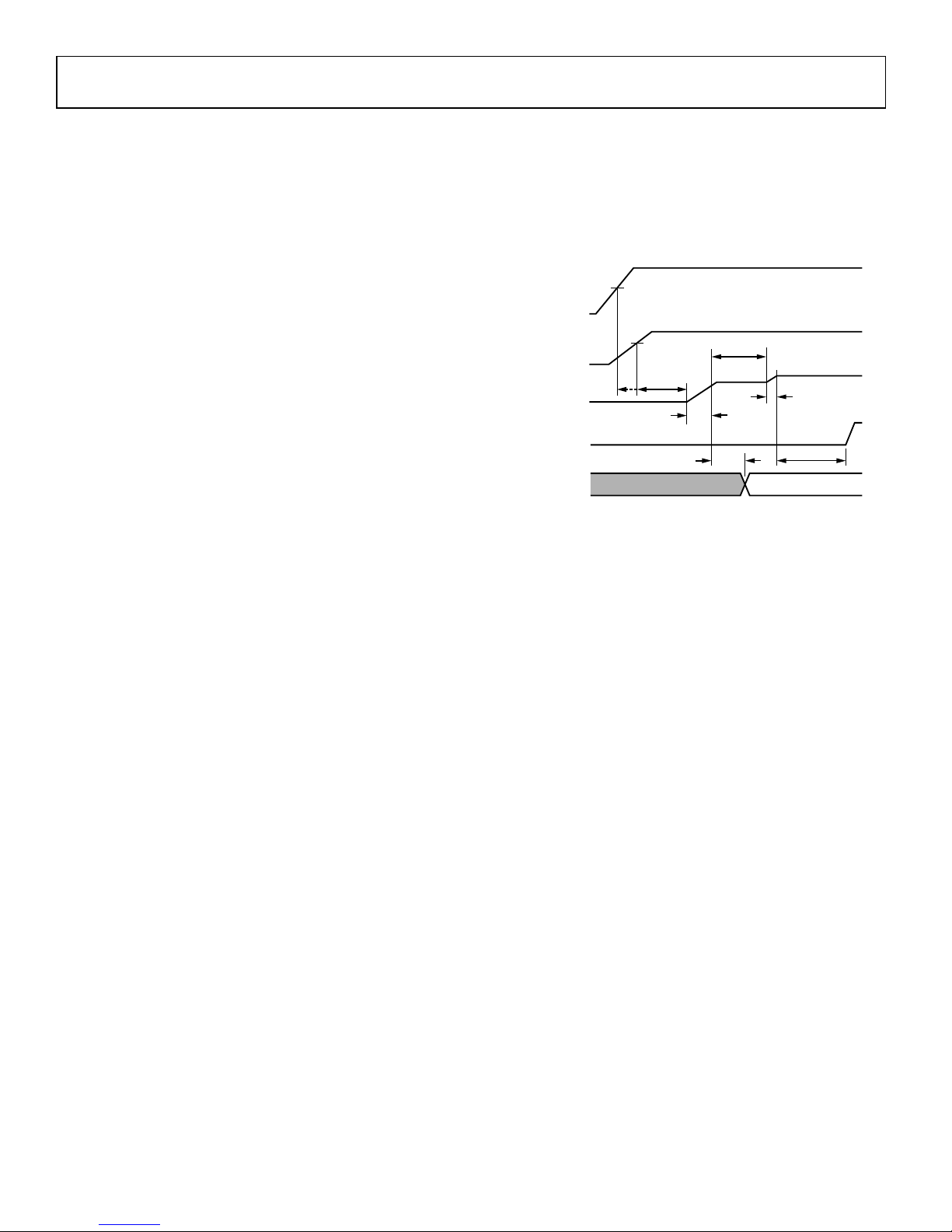
START-UP SEQUENCE
The ASP0800 follows the VR11 start-up sequence shown in
Figure 7. After both the EN and UVLO conditions are met, a
programmable internal timer goes through one cycle TD1. This
delay cycle is programmed using Delay Command, default
delay = 2ms). The first eight clock cycles of TD2 are blanked
from the PWM outputs and used for phase detection as
explained in the following section. Then the programmable
internal soft-start ramp is enabled (TD2) and the output comes
up to the boot voltage of 1.1V. The boot hold time is also set by
the Delay Command. This second delay cycle is called TD3.
During TD3 the processor VID pins settle to the required VID
code. When TD3 is over, the ASP0800 reads the VID inputs
and soft starts either up or down to the final VID voltage
(TD4). After TD4 has been completed and the PWRGD
masking time (equal to VID on the fly masking) is finished, a
third cycle of the internal timer sets the PWRGD blanking
(TD5).
The internal delay and soft start times are programmable using
the serial interface and the Delay Command and Soft Start
Command.
TD1
TD3
TD2
TD5
50µs
TD4
5V
SUPPLY
VTT I/O
(ADP3298 EN)
VCC_CORE
VR READY
(ADP3298 PWRG D)
CPU
VID I NPUTS
VID INVALID VID VALID
V
BOOT
(1.1V)
UVLO
THRESHOL D
0.85V
V
VID
Figure 7. System Start-Up Sequence for VR11
PHASE DETECTION SEQUENCE
During startup, the number of operational phases and their
phase relationship is determined by the internal circuitry that
monitors the PWM outputs. Normally, the ASP0800 operates as
a 8-phase PWM controller.
To operate as a 7-phase controller connect PWM8 to VCC.
To operate as a 6-phase controller connect PWM7 and PWM8
to VCC.
To operate as a 5-phase controller connect PWM6, PWM7 and
PWM8 to VCC.
To operate as a 4-phaase controller connect PWM5, PWM6,
PWM7 and PWM8 to VCC.
To operate as a 3-phase controller connect PWM4, PWM5,
PWM6, PWM7 and PWM8 to VCC.
To operate as a 2-phase controller connect PWM3, PWM4,
PWM5, PWM6, PWM7 and PWM8 to VCC.
To operate as a 1-phase controller connect PWM2, PWM3,
PWM4, PWM5, PWM6, PWM7 and PWM8 to VCC.
Prior to soft start, while EN is low, the PWM8, PWM7, PWM6,
PWM5, PWM4, PWM3 and PWM2 pins sink approximately
100 µA each. An internal comparator checks each pin’s voltage
vs. a threshold of 3 V. If the pin is tied to VCC, it is above the
threshold. Otherwise, an internal current sink pulls the pin to
GND, which is below the threshold. PWM1 is low during the
phase detection interval that occurs during the first eight clock
cycles of TD2. After this time, if the remaining PWM outputs
are not pulled to VCC, the 100 µA current sink is removed, and
they function as normal PWM outputs. If they are pulled to
Downloaded from DatasheetLib.com - datasheet search engine Downloaded from DatasheetLib.com - datasheet search engine
Rev. P1 | Page 11 of 36 | www.onsemi.com
 Loading...