

AND9902/D
Digital IF
Encoder
AX5045 Programming
Manual
Ultra-Low Power Narrow-Band Sub GHz
(60−1050 MHz) RF Transceiver with
Integrated +23 dBm High Power Amplifier
www.onsemi.com
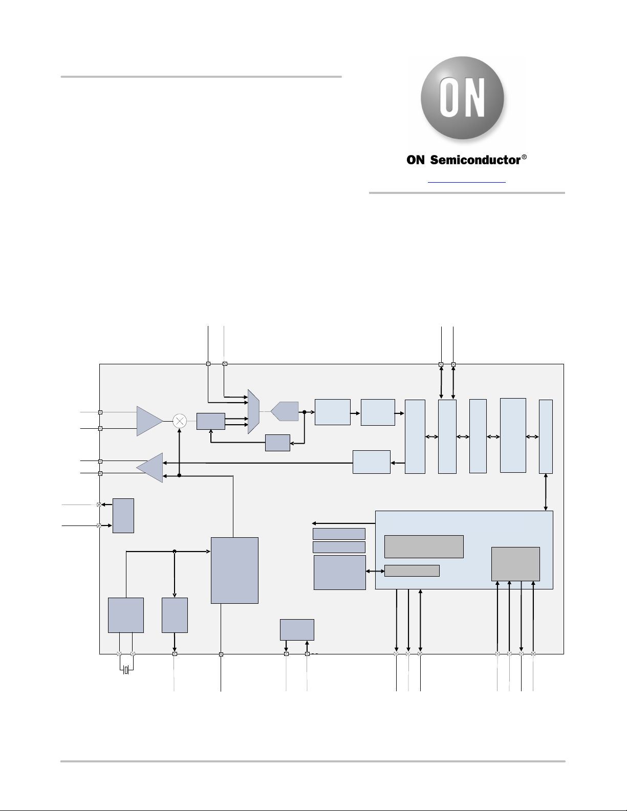
OVERVIEW
AX5045 is a true single chip low-power CMOS
transceiver for narrow band applications. A fully integrated
VCO support most carrier frequencies from 60 MHz to
1050 MHz. The on-chip transceiver consists of a fully
integrated RF front-end with modulator, and demodulator.
Base band data processing is implemented in an advanced
and flexible communication controller that enables user
friendly communication via the SPI interface.
GPADC1
GPADC2
25
26
AX5045
5
VCHOKE
VDD_IO
RX_P
RX_N
TX_P
TX_N
6
3
4
27
1,23
Voltage
Crystal
Oscillator
typ.
16 MHz
28
Regulator
27
LNA
Mixer
IF Filter &
AGC PGAs
PA
OUT
F
XTAL
F
Divider
13
RF Frequency
Generation
Subsystem
RF Output
60 MHz –
1.05 GHz
8
ADC
AGC
Voltage
Regulator
7
APPLICATION NOTE
An on-chip low power oscillator as well as Wake-on-radio
enable very low power standby applications. Figure 1 shows
the block diagram of the AX5045.
DCLK
DATA
12
11
channel
filter
Chip configuration
POR
References
Low Power
Oscillator
640 Hz/10kHz
23,1
De-
modulator
Modulator
Correction
Forward Error
Communication Controller &
Registers
Wake on Radio
19
Serial Interface
Framing
handling
Radio Controller
Radio Controller
timing and packet
timing and packet
SPI
14
FIFO
17
CLKP
CLKN
SYSCLK
© Semiconductor Components Industries, LLC, 2019
March, 2021 − Rev. 1
FILT
VDD_IO
VDD_ANA
IRQ20PWRAMP21ANTSEL
Figure 1. Functional Block Diagram of the AX5045
1 Publication Order Number:
SEL15CLK16MISO
AND9902/D
MOSI

AND9902/D
Table of Contents
Overview 1...............................................................................................
FIFO Operation 7.........................................................................................
Programming the Chip 12..................................................................................
Register Overview 21......................................................................................
Register Details 33........................................................................................
References 82............................................................................................
www.onsemi.com
2
AND9902/D
AX5045
SEL
AX8052F100
or
other mC
28 27 26 25 24 23 22
1
2
3
4
5
6
7
21
20
19
18
17
16
15
8 9 10 11 12 13 14
RESET_N
PB7/DBG_CLK
DBG_EN
PB6/DBG_DATA
PB5/U0RX/T1OUT
PB4/U0TX/T1CLK
PB3/OC0/T2CLK/EXTIRQ1/DSWAKE
RIRQ/PR5
VDD_CORE
RMOSI/PR4
RMISO/PR3
RCLK/PR2
RSEL/PR0
RSYSCLK/PR1
OMPO0/U0RX/SMISO/PC3
U 0T X/S MO SI/P C2
OMPO1/T0CLK/SSCK/PC1
XTIRQ0/T0OUT/SSEL/PC0
EXTIRQ0/IC1/U1TX/PB0
OC1/U1RX/PB1
T2OUT/IC0/PB2
PA5/ADC5/IC0/U1TX/COMPI10
PA4/ADC4/T1CLK/COMPO0/LPXTA
PA3 /AD C3/T 1OU T/LPX TALP
PA 2/A DC 2 /OC 0/U 1R X/C OM PI0 0
PA1/ADC1/T0CLK/OC1/XTALP
PA 0/A DC 0/T 0 OU T/IC 1/X TAL N
VDD_IO
IRQ
MOSI
MISO
CLK
SYSCLK
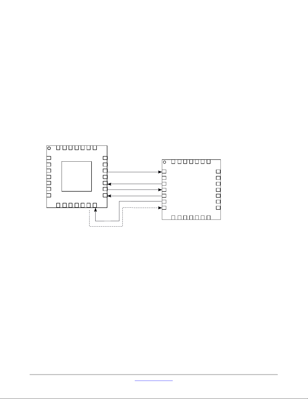
Connecting the AX5045 to an AX8052F100 or other
Microcontroller
The AX5045 can easily be connected to an AX8052F100
or any other microcontroller. The microcontroller
communicates with the AX5045 via a register file that is
implemented in the AX5045 and that can be accessed
serially via an industry standard Serial Peripheral Interface
(SPI) protocol.
Reset is performed by the integrated power-on-reset
(POR) block and can be performed manually via the register
file.
The AX5045 sends and receives data via the SPI port in
frames. This standard operation mode is called frame mode.
NC
NC
VDD_IO
21
ANTSEL
20
PWRAMP
IRQ
19
NC
18
MOSI
17
MISO
16
CLK
15
VDD_IO
VCHOKE
TX_P
TX_N
RX_P
RX_N
VDD_ANA
GPADC2
CLKP
CLKN
28 27 26 25 24 23 22
1
2
3
4
5
6
7
GND
center pad
GPADC1
In frame mode, the internal communication controller
performs frame delimiting, and data is received and
transmitted via a 256 Byte FIFO, accessible via the register
file. The FIFO is shared between receive and transmit.
Figure 2 shows the corresponding diagram. Connecting the
interrupt line is highly recommended, though not strictly
required. It is also recommended to connect the SYSCLK
line, which can be programmed to provide a copy of the
precise crystal clock of the AX5045. Once set up, the
Microcontroller can directly run on that clock or use it to
calibrate its internal oscillators.
810111213149
FILT
NC
NC
SEL
DCLK
DATA
SYSCLK
Figure 2. Connecting AX5045 to AX8052F100 or other mC
www.onsemi.com
3

Pin Function Descriptions
Table 1. PIN FUNCTION DESCRIPTION
Symbol
Pin(s)
Type
Description
VDD_IO1P
Power supply 3.0 V – 3.6 V
VCHOKE2P
Regulator Output to External PA choke inductors
TX_P3A
Differential TX antenna output
TX_N4A
Differential TX antenna output
RX_P5A
Differential RX antenna input
RX_N6P
Differential RX antenna input
VDD_ANA
7
P
Analog power output, decoupling
FILT8A
Optional synthesizer filter
NC9A
Not used
NC10A
Not used
DATA11I/O
In wire mode: Data input/output
DCLK12I/O
In wire mode: Clock output
SYSCLK
13
I/O
Default functionality: Crystal oscillator (or divided) clock output Can be pro-
SEL14I
Serial peripheral interface select
CLK15I
Serial peripheral interface clock
MISO16O
Serial peripheral interface data output
MOSI17I
Serial peripheral interface data input
NC18N
Must be left unconnected
IRQ19I/O
Default functionality: Transmit and receive interrupt
PWRAMP
20
I/O
Default functionality: Power amplifier control output
ANTSEL
21
I/O
Default functionality: Diversity antenna selection output
NC22N
Must be left unconnected
VDD_IO23P
Power supply 3.0 V – 3.6 V
NC24N
Must be left unconnected
GPADC125A
GPADC input, must be connected to GND if not used
GPADC226A
GPADC input, must be connected to GND if not used
CLKN27A
Crystal oscillator input/output. Leave unconnected when using TCXO
CLKP28A
Crystal oscillator input/output. TCXO input.
GND
Center pad
P
Ground on center pad of QFN, must be connected
AND9902/D
Can be programmed to be used as a general purpose I/O pin Selectable
internal 65 kW pull−up resistor
Can be programmed to be used as a general purpose I/O pin Selectable
internal 65 kW pull−up resistor
grammed to be used as a general purpose I/O pin Selectable internal 65 kW
pull−up resistor
Can be programmed to be used as a general purpose I/O pin Selectable
internal 65 kW pull−up resistor
Can be programmed to be used as a general purpose I/O pin Selectable
internal 65 kW pull−up resistor
Can be programmed to be used as a general purpose I/O pin Selectable
internal 65 kW pull−up resistor
NOTE: All digital inputs are Schmitt trigger inputs, digital input and output levels are LVCMOS/LVTTL compatible and 5 V tolerant.
A = analog input
I = digital input signal
O = digital output signal
I/O = digital input/output signal
N = not to be connected
P = power or ground
www.onsemi.com
4
AND9902/D
Table 2. SPI STATUS BITS
SPI Bit Cell
Status
Register Bit
0
−
1 (when transitioning out of deep sleep, this bit transitions from 0→1 when the power becomes ready)
1
S14
PLL LOCK
2
S13
FIFO OVER
3
S12
FIFO UNDER
4
S11
THRESHOLD FREE ( FIFO Free > FIFO threshold)
5
S10
THRESHOLD COUNT (FIFO count > FIFO threshold)
6
S9
FIFO FULL
7
S8
FIFO EMPTY
8
S7
PWRGOOD (not BROWNOUT)
9
S6
PWR INTERRUPT PENDING
10
S5
RADIO EVENT PENDING
11
S4
XTAL OSCILLATOR RUNNING
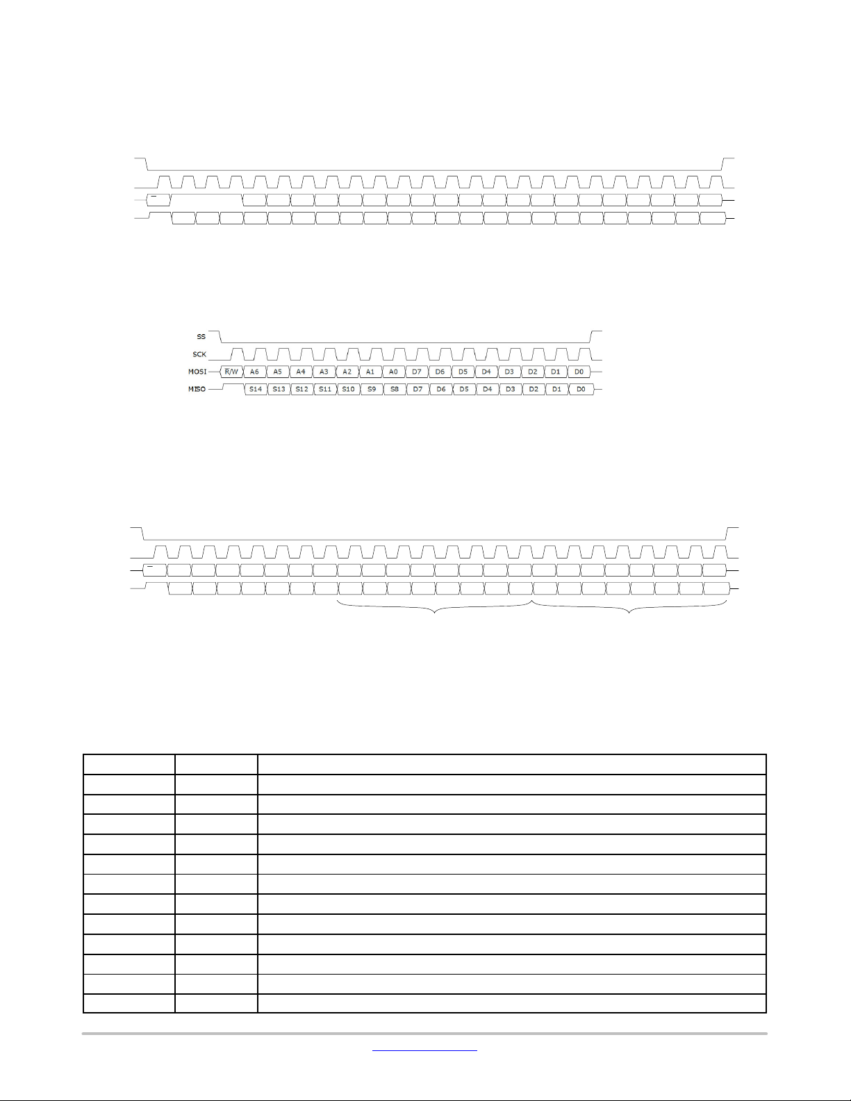
SPI Register Access
Registers are accessed via a synchronous Serial Peripheral
Interface (SPI). Most Registers are 8 bits wide and accessed
using the waveforms as detailed in Figure 3. These
SS
SCK
R/W A7S7A6 A5 A4 A3 A2 A1
MOSI
MISO
S14 S13 S12 S11 S9A8S8
A11 A10 A9
111
S6 S5 S4 S3 S2 S1A0S0
Figure 3. SPI 8bit Long Address Read/Write Access
The most important registers are at the beginning of the
address space, i.e. at addresses less than 0x70. These
Figure 4. SPI 8bit Read/Write Access
Some registers are longer than 8 bits. These registers can
be accessed more quickly than by reading and writing
individual 8 bit parts. This is illustrated in Figure 5. Accesses
are not limited by 16 bits either, reading and writing data
waveforms are compatible to most hardware SPI master
controllers, and can easily be generated in software. MISO
changes on the falling edge of CLK, while MOSI is latched
on the rising edge of CLK.
D7 D6 D5 D4 D3 D2 D1 D0
D7 D6 D5 D4 D3 D2 D1 D0S10
registers can be accessed more efficiently using the short
address form, which is detailed in Figure 4.
bytes can be continued as long as desired. After each byte,
the address counter is incremented by one. Also, this access
form also works with long addresses.
SS
SCK
R/W A6 A5 A4 A3 A2 A1 A0
MOSI
MISO
S14 S13 S12 S11 S10 S9 S8
D7 D6 D5 D4 D3 D2 D1 D0
D7 D6 D5 D4 D3 D2 D1 D0
Figure 5. SPI 16bit Read/Write Access
During the address phase of the access, the chip outputs
the most important status bits. This feature is designed to
speed up software decision on what to do in an interrupt
D7 D6 D5 D4 D3 D2 D1 D0
D7 D6 D5 D4 D3 D2 D1 D0
A A+1
handler. The table below shows which register bit is
transmitted during the status timeslots.
www.onsemi.com
5

Table 2. SPI STATUS BITS (continued)
12
S3
WAKEUP INTERRUPT PENDING
13
S2
LPOSC INTERRUPT PENDING
14
S1
GPADC INTERRUPT PENDING
15
S0
undefined
SPI Bit Cell Register BitStatus
AND9902/D
Note that bit cells 8−15 (S7…S0) are only available in two
address byte SPI access formats.
Deep Sleep
The chip can be programmed into deep sleep mode. In
deep sleep mode, the chip is completely switched off, which
results in very low leakage power. All registers loose their
programming.
To enter deep sleep mode, write the deep sleep encoding
into bits 3:0 of PWRMODE. At the rising edge of the SEL
line, the chip will enter deep sleep mode.
To exit deep sleep mode, lower the SEL line. This will
initiate startup and reset of the chip. Then poll the MISO
line. The MISO line will be held low during initialization,
and will rise to high at the end of the initialization, when the
chip becomes ready for further operation.
Address Space
The address space has been allocated as follows.
Addresses from 0x000 to 0x06F are reserved for “dynamic
registers”, i.e. registers that are expected to be frequently
accessed during normal operation, as they can be efficiently
accessed using single address byte SPI accesses. Addresses
from 0x070 to 0x0FF have been left unused (they could only
be accessed using the two address byte SPI format).
Addresses from 0x100 to 0x1FF have been reserved for
physical layer parameter registers, for example receiver,
transmitter, PLL, crystal oscillator. Addresses from 0x200 to
0x2FF have been reserved for medium access parameters,
such as framing, packet handling. Addresses from 0x300 to
0x3FF have been reserved for special functions, such as
GPADC.
www.onsemi.com
6
FIFO OPERATION
Table 3. CHUNK PAYLOAD SIZE ENCODING
Top Bits
Chunk Payload Size
000
No payload
001
Single byte payload
010
Two byte payload
011
Three byte payload
AND9902/D
The AX5045 features a 256 Byte FIFO. The same FIFO
is used for both reception and transmission. During transmit,
only the write port is accessible by the microcontroller.
During receive, only the read port is accessible by the
microcontroller. Otherwise, both ports are accessible
through the register file.
In order to prevent transmitting premature data, the FIFO
contains three pointers. Data is read at the read pointer, up
to the write pointer. Data is written to the write ahead pointer .
The write pointer is not updated when data is written,
therefore, new data is not immediately visible to the
consumer. Writing the COMMIT command to the
FIFOSTAT register copies the write ahead pointer to the
write pointer, thus making the written data visible to the
Write ahead pointer
Write pointer
FIFOCOUNT
receiver. Writing the ROLLBACK command to the
FIFOSTAT register sets the write ahead pointer to the write
pointer, thus discarding data written to the FIFO. During
transmit, this means that the transmitter will only consider
data written to the FIFO after the commit command. During
receive, this feature is used by the receiver to store packet
data before it is known whether the CRC check passes.
FIFOCOUNT reports the number of bytes that can be read
without causing an underflow. FIFOFREE reports the
number of bytes that can be written without causing an
overflow. FIFOCOUNT and FIFOFREE do not add up to
256 Bytes whenever there are uncommitted bytes in the
FIFO. Figure 6 illustrates this.
256−FIFOFREE
Figure 6. FIFO Pointer
FIFO Chunk Encoding
In order to distinguish meta-data (such as RSSI) from
receive or transmit data, FIFO contents are organized as
chunks. Chunks consist of a header that encodes the chunk
length as well as the payload data format.
Each chunk starts with a single byte header. The header
encodes the length of a chunk, and indicates the data it
contains. The top 3 bits encode the length (or optionally refer
to an additional length byte after the header byte), and the
bottom 5 bits indicate what payload data the chunk contains.
The following table lists the encoding of the length bits (top
3 bits of the first chunk header byte). Figure 7 shows the
chunk header byte encoding.
Read pointer
76543210
Chunk
payload
size
Figure 7. FIFO Header byte Format
Chunk
payload
data format
The following table lists the chunk payload size encoding:
www.onsemi.com
7
AND9902/D
100
Invalid
101
Invalid
110
Invalid
111
Variable length payload; payload size is encoded in the following length byte the length byte is part of
Table 4. CHUNK TYPES AND THEIR ENCODINGS
Hdr. Byte
7−0
No Payload Commands
T
00000000
No Operation
T
00000011
Trigger a Radiocontrol
One Byte Payload Commands
R
00110001
RSSI
T
00111100
Transmit Control
Two Byte Payload Commands
R
01010010
Frequency Offset
R
01010101
Background Noise
Three Byte Payload Commands
T
01100010
Repeat Data
TR
01110000
Timer
R
01110011
RF Frequency Offset
R
01110100
Datarate
R
01110101
Antenna Selection RSSI
Variable Length Payload Commands
TR
11100001
Data
T
11111101
Transmit Power
Table 5. NOP COMMAND
7654321
0
0000000
0
Table 6. FIFOIRQ COMMAND
7654321
0
0000001
1
Table 7. RSSI COMMAND
765432100011000
1
RSSI
Table 8. TXCTRL COMMAND
765432100011110
0
0
Table 3. CHUNK PAYLOAD SIZE ENCODING (continued)
Top Bits Chunk Payload Size
the header (and not included in length), everything after the length byte is included in the length
The following table lists the chunk types and their
encodings. The Hdr Byte column lists the complete FIFO
Chunk Header Byte, consisting of the length and data format
encodings.
Name Dir
NOP
FIFOIRQ
RSSI
TXCTRL
FREQOFFS
ANTRSSI2
REPEATDATA
TIMER
RFFREQOFFS
DATARATE
ANTRSSI3
Description
interrupt
(Antenna, Power Amp)
Calculation RSSI
FIFOIRQ Command
The FIFOIRQ command triggers an interrupt if bit
IRQMRADIOCTRL is set in register IRQMASK0 and bit
REVMFIFOIRQCMDDET is set in register
RADIOEVENTMASK. This feature allows to track TX
events as for example completion of preamble transmission.
To clear the interrupt, register RADIOEVENTREQ0 has
to be read.
RSSI Command
The RSSI command will only be generated by the receiver
at the end of a packet if bit ST RSSI is set in register
PKTSTOREFLAGS. The encoding is the same as that of the
RSSI register.
TXCTRL Command
DATA
TXPWR
Direction: T = Transmit, R = Receive
NOP Command
SETTX TXSE TXDIFF SETANT ANTSTATE SETPA PASTATE
The TXCTRL command allows certain aspects of the
transmitter to be changed on the fly. If SETTX is set, TXSE
and TXDIFF are copied into the register MODCFGA. If
SETANT is set, ANTSTATE is copied into register
DIVERSITY. If SETPA is set, PASTATE is copied into
register PWRAMP.
The NOP command will be discarded without effect by
the transmitter. The receiver will not generate NOP
commands.
www.onsemi.com
8
AND9902/D
Table 9. FREQOFFS COMMAND
7654321
0
0101001
0
FREQOFFS1
FREQOFFS0
Table 10. ANTRSSI2 COMMAND
7654321
0
0101010
1
RSSI
BGNDNOISE
Table 11. REPEATDATA COMMAND
765432100110001
0
0
DIBITSYNC
UNENC
RAW
NOCRC
RESIDUE
PKTEND
PKTSTART
REPEATCNT
DATA
Table 12. TIMER COMMAND
7654321
0
0111000
0
TIMER2
TIMER1
TIMER0
Table 13. RFFREQOFFS COMMAND
765432100111001
1
RFFREQOFFS2
RFFREQOFFS1
RFFREQOFFS0
Table 14. DATARATE COMMAND
7654321
0
0111010
0
DATARATE2
DATARATE1
DATARATE0
FREQOFFS Command
The FREQOFFS command will only be generated by the
receiver at the end of a packet if bit ST FOFFS is set in
register PKTSTOREFLAGS. The encoding is the same as
that of the TRKFREQ register.
REPEATDATA Command
ANTRSSI2 Command
The ANTRSSI2 command will be generated by the
receiver when it is idle if bit ST ANT RSSI is set in register
PKTSTOREFLAGS. If DIVENA is set in register
DIVERSITY, the ANTRSSI3 command is generated
instead. The encoding of the RSSI field is the same as that
of the RSSI register. The BGNDNOISE field contains an
estimate of the background noise.
The REPEATDATA command allows the efficient
transmission of repetitive data bytes. The DATA byte given
in the payload is repeated REPEATCNT times. See DATA
command for a description of the flag byte. This command
is especially handy for constructing preambles.
TIMER Command
This command enables exact packet timing, e.g. for
frequency hopping systems.
In TX mode, upon detection of a TIMER command, the
transmitter pauses until the internal timer (accessible via
TIMER register) reaches the value given by the payload. A
detailed documentation of this function can be found under
the description of register RCTRLTIMESTAMP.
In RX mode, the TIMER command will be generated by
the receiver at the start/end of a packet if bit ST TIMER
and/or ST TIMER PKTEND is set in register
PKTSTOREFLAGS. The payload is a copy of the internal
timer (i.e. the current value of the TIMER register).
RFFREQOFFS Command
The RFFREQOFFS command will only be generated by
the receiver at the end of a packet if bit ST RFOFFS is set in
register PKTSTOREFLAGS. The encoding is the same as
that of the TRKRFFREQ register.
DATARATE Command
The DATARATE command will only be generated by the
receiver at the end of a packet if bit ST DR is set in register
PKTSTOREFLAGS. The encoding is the same as that of the
TRKDATARATE register.
www.onsemi.com
9
AND9902/D
Table 15. ANTRSSI3 COMMAND
7654321
0
0111010
1
ANTORSSI2
ANTORSSI1
ANTORSSI0
Table 16. TRANSMIT DATA FORMAT
7654321
0
1110000
1
LENGTH
0
DIBITSYNC
UNENC
RAW
NOCRC
RESIDUE
PKTEND
PKTSTART
DATA
Table 17. FIFO COMMAND
0xE1
FIFO Command
0x04
Length Byte
0x24
Flag Byte: Unencoded, to ensure 0−1 remains 0−1, and Residue set, because the number of bits
0xAA
Alternating 0−1 bits
0xAA
Alternating 0−1 bits
0x1A
Alternating 0−1 bits; Bit 4 is the “Stop” bit
Table 18. RECEIVE DATA FORMAT
7654321
0
1110000
1
LENGTH
SYNCWD
ABORT
SIZEFAIL
ADDRFAIL
CRCFAIL
RESIDUE
PKTEND
PKTSTART
DATA
ANTRSSI3 Command
The ANTRSSI3 command will be generated by the
receiver when it is idle if bit ST ANT RSSI is set in register
LENGTH includes the flags byte as well as all DATA
bytes.
Setting RAW to one causes the DATA to bypass the
framing mode, but still pass through the encoder.
Setting UNENC to one causes the DATA to bypass the
framing mode, as well as the encoder, except for inversion.
UNENC has priority over RAW.
Setting NOCRC suppresses the generation of the CRC
bytes.
Setting RESIDUE allows the transmission of a number of
data bits that is not a multiple of eight. All but the last data
byte are transmitted as if RESIDUE was not set. The last
byte however contains only 7 bits or less. The transmitter
looks for the highest bit set. This is considered the stop bit.
Only bits below the stop bit are transmitted. If the
MSBFIRST in re g ister PKTADDRCFG is set, the algorithm
PKTSTOREFLAGS. If DIVENA is not set in register
DIVERSITY, the ANTRSSI2 command is generated
instead. The encoding of the ANT0RSSI and ANT1RSSI
fields are the same as that of the RSSI register.
The BGNDNOISE field contains an estimate of the
background noise.
DATA Command
The DATA command transports actual transmit and
receive data. While the basic format is the same for transmit
and receive, the semantics of the flag byte differs.
is reversed, i.e. the lowest bit set is considered the stop bit
and bits above the stop bit are transmitted.
PKTSTART and PKTEND bits enable the transmission of
packets that are larger than the FIFO size. If PKTSTART is
set, the radio packet starts at the beginning of the DATA
command payload. If PKTEND is set, the radio packet ends
at the end of the DA TA command payload. If PKTSTART is
not set, this command is the continuation of a previous
DATA command. If PKTEND is not set, the packet is
continued with the next DATA command.
Setting DIBITSYNC causes the DATA bytes to be aligned
to DiBit boundaries in 4−FSK mode.
For example, to transmit 20 bits of an alternating 0−1
pattern as a preamble, the following bytes should be written
to the FIFO (MSBFIRST = 0 in register PKTADDRCFG is
assumed):
transmitted is not a multiple of 8
www.onsemi.com
10

AND9902/D
Table 19. TXPWR COMMAND
7654321
0
1111001
0
LENGTH = 10
TXPWRCOEFFA (7:0)
TXPWRCOEFFA (15:8)
TXPWRCOEFFB (7:0)
TXPWRCOEFFB (15:8)
TXPWRCOEFFC (7:0)
TXPWRCOEFFC (15:8)
TXPWRCOEFFD (7:0)
TXPWRCOEFFD (15:8)
TXPWRCOEFFE (7:0)
TXPWRCOEFFE (15:8)
ABOR T i s set if the packet has been aborted. An ABORT
sequence is a sequence of seven or more consecutive one bits
when HDLC [1] framing is used. Note that if ACCPT ABR T
is not set in register PKTACCEPTFLAGS, then aborted
packets are silently dropped.
SIZEFAIL is set if the packet does not pass the size
checks. Size checks are implemented using the
PKTLENCFG, PKTLENOFFSET and PKTMAXLEN
registers. Note that if ACCPT SZF is not set in register
PKTACCEPTFLAGS, then packets with an invalid size are
silently dropped.
ADDRFAIL is set if the packet does not pass the address
checks. Address checks are implemented using the
PKTADDRCFG, PKTADDRA, PKTADDRB,
PKTADDRENA and PKTADDRMASK registers. Note that
if ACCPTADDRF is not set in register
PKTACCEPTFLAGS, then packets which do not match the
programmed address are silently dropped.
CRCF AIL i s set if the packet does not pass the CRC check.
Note that if ACCPTCRCF is not set in register
PKTACCEPTFLAGS, then packets which fail the CRC
check are silently dropped.
RESIDUE, PKTEND and PKTSTART work identical as
in transmit mode, see above.
The receiver generates chunks up to PKTCHUNKSIZE
bytes. If PKTMAXLEN is larger than PKTCHUNKSIZE,
multiple chunks may be generated for one packet. Since
CRC and size checks may only be performed at the end of
the packet, only the last chunk can be dropped at failure of
one of those tests. It is therefore important that the
microcontroller receiver routine clears its receive buffer at
the beginning of DATA commands whose PKTSTART bit
is set, as the buffer may still contain bytes from erroneous
packets.
TXPWR Command
The TXPWR command allows the transmit power to be
changed on the fly. This command updates the
TXPWRCOEFFA, TXPWRCOEFFB, TXPWRCOEFFC,
TXPWRCOEFFD and TXPWRCOEFFE registers.
www.onsemi.com
11

PROGRAMMING THE CHIP
Table 20. PWRMODE REGISTER STATES
PWRMODE register
Name
Description
Typical Idd
0000
POWERDOWN
Powerdown; all circuits powered down except for the register file
640 nA
0001
DEEPSLEEP
Deep Sleep Mode; Chip is fully powered down until SEL is lowered
121 nA
0101
STANDBY
Crystal Oscillator enabled
960μA
0111
FIFOON
FIFO enabled (Crystal Oscillator enabled by setting bit XOEN in
1010μA
1000
SYNTHRX
Synthesizer running, Receive Mode
7mA
1001
FULLRX
Receiver Running
14-17 mA
1011
WORRX
Receiver Wake-on-Radio Mode
700 nA
1100
SYNTHTX
Synthesizer running, Transmit Mode
7mA
1101
FULLTX
Transmitter Running at 23 dBm
255 mA
AND9902/D
Power Modes
To enable the lowest possible application power
consumption, the AX5045 allows to shut down its circuits
again; looses all register contents
register PWRMODE)
The following list explains the typical programming flow.
Preparation:
1. Reset the Chip. Set SEL to high for at least 1μs,
then low. Wait until MISO goes high. Set, and then
clear, the RST bit of register PWRMODE.
2. Set the PWRMODE register to POWERDOWN.
3. Program parameters. It is recommended that
suitable parameters are calculated using the
AX−RadioLab tool available at onsemi.com
.
4. Perform auto-ranging, to ensure the correct VCO
range setting.
The chip is now ready for transmit and receive operations.
FIFO Power Management
The FIFO is powered down during POWERDOWN and
DEEPSLEEP modes (Register PWRMODE). Reads to
register FIFOSTAT will provide bit FIFO EMPTY as one
and bit FIFO FULL as zero. Registers FIFOCOUNT and
FIFOFREE read zero as well. Reads from the FIFO will
return undefined data, and writes to the FIFO will be lost.
In the receive case, the FIFO is automatically powered on
when the chip PWRMODE is set to FULLRX. The FIFO
should be emptied before the PWRMODE is set to
POWERDOWN. In Wake-on-radio or POWERDOWN
when not needed. This is controlled by the PWRMODE
register. Idd values are typical; for exact values, please refer
to the AX5045 datasheet [2].
mode, the FIFO is automatically kept powered on until it is
emptied by the microprocessor.
In the transmit case, PWRMODE should first be set to
FULLTX. Before writing to the FIFO, the microprocessor
must ensure that the SVMODEM bit is high in Register
POWSTAT, to ensure that the on-chip voltage regulator
supplying the FIFO has finished starting up. The transmitter
remains idle until the contents of the FIFO are committed
(unless the FIFO AUTO COMMIT bit is set in Register
FIFOSTAT).
Autoranging
Whenever the frequency changes, the synthesizer VCO
should be set to the correct range using the built-in autoranging. A re-ranging of the VCO is required if the
frequency change required is la r ger than 0.5 MHz divided by
the RF Divider Ratio resulting from the RFDIV setting in
register PLLVCODIV. Each individual chip must be
auto-ranged. If both frequency register sets FREQA and
FREQB are used, then both frequencies must be auto-ranged
by first starting auto-ranging in PLLRANGINGA, waiting
for its completion, followed by starting auto-ranging in
PLLRANGINGB and waiting for its completion.
www.onsemi.com
12
AND9902/D
Table 21. FUNDAMENTAL COMMUNICATION CHARACTERISTIC
Parameter
Description
f
Frequency of the connected crystal/TCXO in Hz
modulation
PSK, ASK, FSK, MSK, OQPSK, 4−FSK or AFSK (for recommendations see below)
f
Carrier frequency (i.e. center frequency of the signal) in Hz
BITRATE
Desired bit rate in bit/s
h
Modulation index, determines the frequency deviation for FSK
encoding
Inversion, differential, Manchester, scrambled, for recommendations see the description of the register
Table 22. TRADE-OFFS BETWEEN THE DIFFERENT MODULATION
Modulation
Trade-offs
FSK
For bit rates up to 125 kbit/s; 200 kbit/s possible with some limitations*
ASK
For bit rates up to 50 kbit/s;
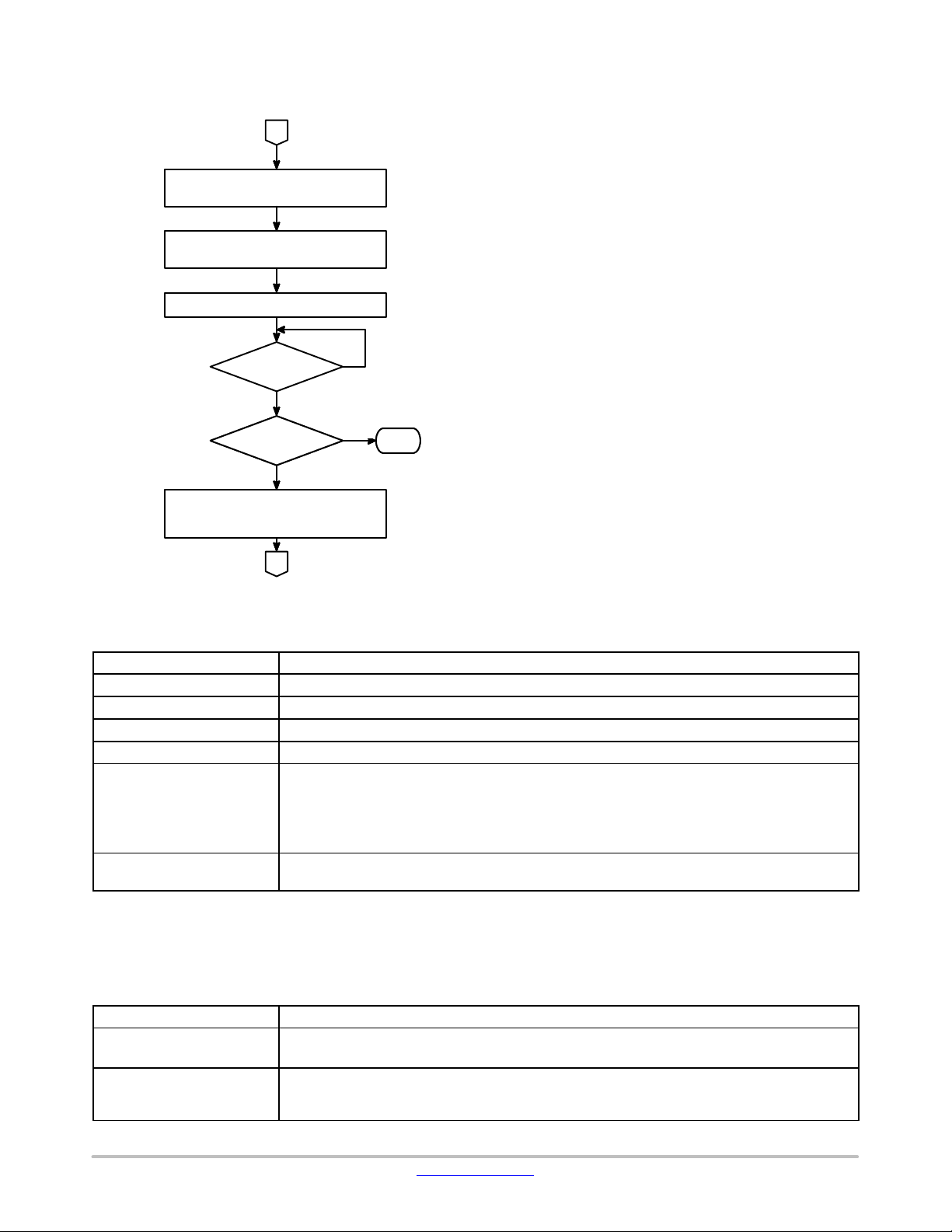
Figure 8 shows the flow chart of the auto-ranging process.
Set PWRMODE to STANDBY
Enable TCXO if used
Wait until crystal oscillator
Set RNGSTART of PLLRANGINGA/B
Set PWRMODE to POWERDOWN
is ready
RNGSTART = 1?
no
RNGERR = 1?
no
Disable TCXO if used
yes
yes
Error
Before starting the auto-ranging, the appropriate
frequency registers (FREQA or FREQB) need to be
programmed. Auto-ranging starts at the VCOR (register
PLLRANGINGA or PLLRANGINGB) setting;
if you already know the approximately correct synthesizer
VCO range, you should set VCORA/VCORB to this value
prior to starting auto-ranging; this can speed up the ranging
process considerably. The autoranging feature will not
increment/decrement the MSB so preset this to the
appropriate range prior to setting the RNGSTART bit.
Hardware clears the RNG START bit automatically as
soon as the ranging is finished; the device may be
programmed to deliver an interrupt on resetting of the RNG
START bit.
Waiting until auto-ranging terminates can be performed
by either polling the register PLLRANGINGA1 or
PLLRANGINGB1 for RNG START to go low, or by
enabling the IRQMPLLRNGDONE interrupt in register
IRQMASK1.
Choosing the Fundamental Communication
Characteristics
The following table lists the fundamental communication
characteristics that need to be chosen before the device can
be programmed.
Figure 8. Autoranging Flow Chart
XTAL
CARRIER
32 > h ≥ 0.5 for FSK, 4−FSK or AFSK, f
h = 0.5 for MSK and OQPSK
(For AFSK, f
often approximately 3 kHz)
ENCODING.
is usually set according to the FM channel specification. For 25 kHz channels, it is
deviation
The following table gives an overview of the trade-offs
between the different modulations that AX5045 offers, they
should be considered when making a choice.
= 0.5 * h * BITRATE
deviation
Frequency deviation is a free parameter
ASK is spectrally more efficient than FSK, but also more susceptible to noise and can only be
demodulated with lower sensitivity.
www.onsemi.com
13

AND9902/D
MSK
For bit rates up to 125 kbit/s; 200 kbit/s possible with some limitations*
OQPSK
For bit rates up to 125 kbit/s; 200 kbit/s possible with some limitations*
PSK
For bit rates up to 10 kbit/s;
4−FSK
For bit rates up to 100 kSymbols/s, or 200 kbit/s possible with some limitations*
AFSK
For bit rates up to 25 kbit/s
x16+x12+x5+1
16
32
5
Table 22. TRADE-OFFS BETWEEN THE DIFFERENT MODULATION (continued)
Modulation Trade-offs
Robust and spectrally efficient form of FSK (Modulation is the same as FSK with h = 0.5)
Frequency deviation given by bit rate
The advantage of MSK over FSK is that it can be demodulated with higher sensitivity.
Slightly longer preambles required than for FSK
Very similar to MSK, with added precoding / postdecoding
For new designs, use MSK instead
Spectrally efficient and high sensitivity
Very accurate frequency reference (maximum carrier frequency deviation ±
preambles required
Similar to FSK, but four frequencies are used to transmit 2 bits simultaneously
Very slightly more spectrally efficient compared to FSK
((1 + 3 h/2) ⋅ BITRATE versus (1 + h) ⋅ BITRATE) for small h.
Longer preambles required as frequency offset estimation needs to be more precise to successfully
demodulate
For new designs, use FSK instead
Bits are FSK modulated in the audio band, then frequency modulated on the carrier frequency.
For legacy compatibility applications only.
*To receive at a data rate of 200 kbit/s, a reference clock between 32 and 50 MHz is required. The ADC clock needs to be configured to by 1/2
the reference clock. This causes the ADC to sample at 2 MSPS instead of 1 MSPS and is required for receiving at the higher data rates. The
ADC sample rate should still be configured as 2 MSPS in all setup configurations. Also, when receiving with higher datarates, care must be
taken to increase the RX bandwidth accordingly (see BBTUNE Register). Also note that the higher sample rate will result in increased current
consumption of 1−1.5 mA, due to increased clocking. In order to transmit at the higher data rates, care must be taken to ensure the PLL loop
bandwidth is wide enough to handle the modulation properly.
Given these fundamental physical layer parameters,
AX_RadioLab should be used to compute the register
settings of the AX5045.
Framing
Figure 1 shows the block diagram of the AX5045. After
the user writes a transmit packet into the FIFO, the Radio
Controller sequences the transmitter start-up, and signals the
Packet Controller to read the packet from the FIFO and add
framing bits, allowing the receiver to lock to the transmit
waveform, and to detect packet and byte boundaries. If MSB
first is selected (register PKTADDRCFG), then the bits
within each byte are swapped when the data is read out from
the FIFO.
The Packet Controller also (optionally) adds cyclic
redundancy check (CRC) bits at the end of the packet, to
enable the receiver to detect transmission errors. Both 16
and 32 Bit CRC can be selected, as well as different
generator polynomials. The CRC polynomial can be
selected in register CRCCFG. The following polynomials
are supported:
• CRC-CCITT (16bit):
(hexadecimal: 0x1021)
• CRC-16 (16bit):
x
+ x15+ x2+1
(hexadecimal: 0x8005)
1
/4 ⋅ BITRATE) and long
• CRC-DNP (16bit):
16
+ x13+ x12+ x11+ x10+ x8+ x6+ x5+ x2+1
x
(hexadecimal: 0x3D65)
This polynomial is used for Wireless M-Bus.
• CRC-32 (32bit):
x
+ x26+ x23+ x22+ x16+ x12+ x11+ x10+ x8+ x7+
4
5
x
+
x
+ x2+x+
(hexadecimal: 0x04C11DB7)
1
The CRC is always transmitted MSB first regardless of
the MSB first setting of register PKTADDRCFG, to enable
the receiver to process CRC bits as they arrive (otherwise,
they would have to be stored and reordered). For an in-depth
guide on how CRC’s are computed, see [3].
By default, the CRC bits are inverted so that erroneously
appended zero−bits can be detected. Skipping this inversion
is not recommended, but it can be achieved by setting bit
CRCNOINV in register CRCCFG.
Finally, the encoder is able to perform certain bit-wise
operations on the bit-stream:
• Manchester:
Manchester transmits a one bit as 10 and a zero bit as
01, i.e. it doubles the data rate on the radio channel. Its
advantage is that the resulting bit-stream has many
transitions and thus simplifies synchronizing to the
www.onsemi.com
14
AND9902/D
transmission on the receiver side. The downside is that
it now requires twice the amount of energy for the
transmission. Manchester is not recommended, except
for compatibility with legacy systems.
• Scrambler:
The scrambler ensures that even highly regular transmit
data results in a seemingly random transmitted
bit-stream. This avoids discrete tones in the spectrum.
Three different scrambling polynomials can be selected
(PN9, PN15, PN17) and it is possible to choose
between additive or multiplicative (self−synchronizing)
scrambling. Do not confuse the scrambler with
encryption – it does not provide any secrecy, its actions
are easily reversed. Its use is recommended, particularly
multiplicative scrambling.
• Differential:
Differential transmits zero bits as constant level, and
one bits as level change. This allows to accommodate
modulations that can invert the bit-stream, such as PSK.
• Inversion:
If on, the bit-stream is inverted. Useful for example for
compatibility with legacy systems, such as POCSAG,
which differ from the usual convention that the higher
FSK frequency signifies a one.
powers up the synthesizer and settles it (registers
TMGTXBOOST and TMGTXSETTLE determine the
timing). The Preamble and the Packet(s) are then
transmitted, followed by the transmitter and synthesizer
shut-down.
The transmitter is automatically ramped up and down
smoothly, to prevent unwanted spurious emissions. The
ramp time is normally one bit time, but may be longer by
changing the SLOWRAMP field of register MODCFGA.
The PWRMODE register should stay at FULLTX until
the transmission is fully completed. The end of the
transmission may be determined by polling the register
RADIOSTATE until it indicates idle, or by enabling the
radio controller interrupt (bit IRQMRADIOCTRL) in
register IRQMASK0 and setting the radio controller to
signal an interrupt at the end of transmission (bit
REVMDONE of register RADIOEVENTMASK0).
Set PWRMODE to FULLTX
Enable TCXO if used
The encoder is controlled using the register ENCODING.
It may be temporarily bypassed except for the inversion by
setting the UNENC bit of the FIFO chunks DATA or
REPEATDATA. This is useful for synthesizing preambles.
The receiver performs these tasks in reverse order.
Transmitter
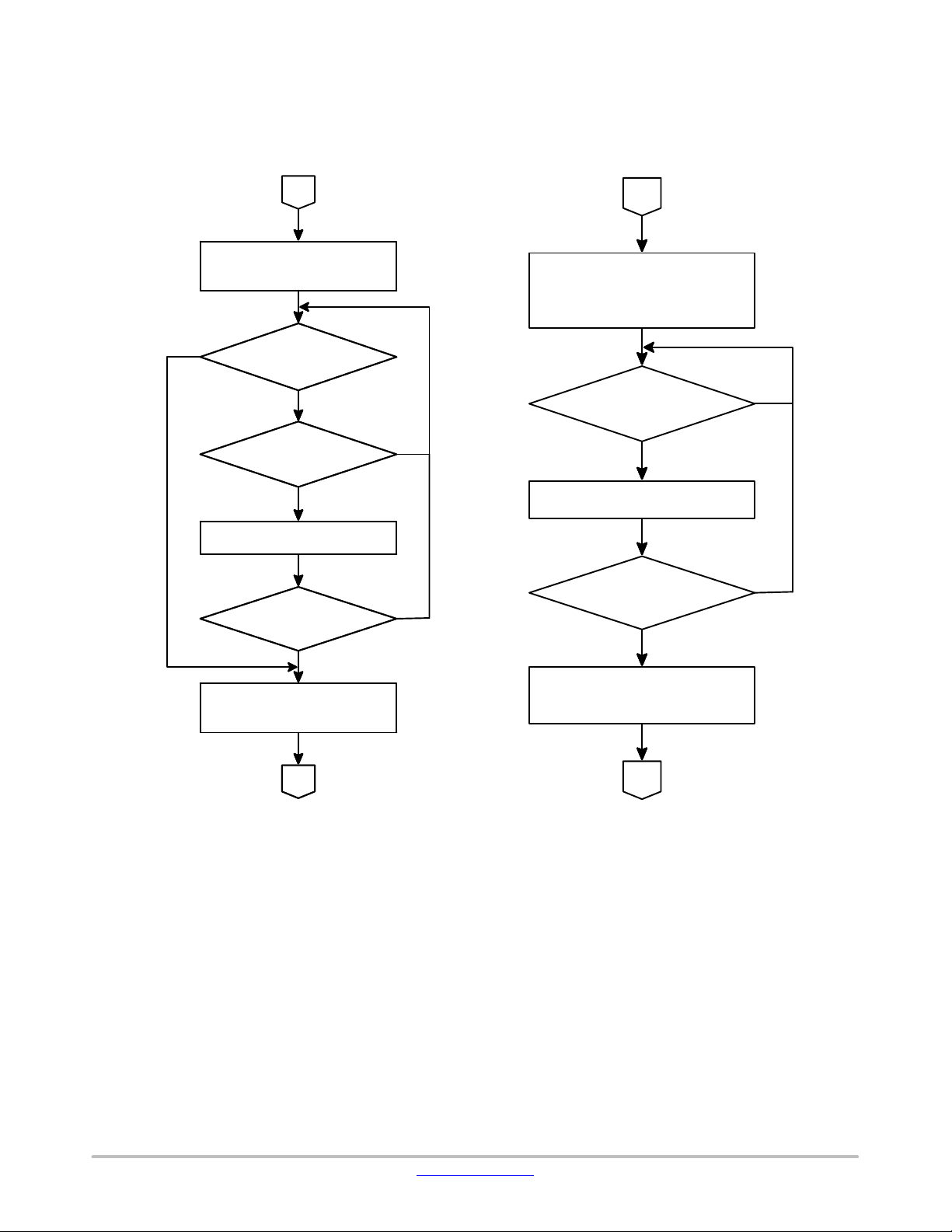
Figure 9 shows the transmitter flow chart. The
microprocessor first places the chip into FULLTX mode.
This prepares the chip for a future transmission, enables the
FIFO in transmit direction, but does not yet power-up the
synthesizer or any other transmit circuitry.
The microprocessor can now write the preamble and the
actual packet to the FIFO. The preamble is programmable to
allow standards to be implemented that specify a specific
preamble to be used. Otherwise, the recommendations for
preambles can be found below.
Waiting for the crystal oscillator to start up may be
performed by polling the register XTALSTATUS, or by
enabling the IRQMXTALREADY interrupt in register
IRQMASK1.
After the FIFO contents are committed (writing the
Commit command to the FIFOSTAT register), the
transmitter notices that the FIFO is no longer empty. It then
Write Preamble to FIFO
Write Packet to FIFO
Wait until crystal oscillator
Wait until transmission is done
Set PWRMODE to POWERDOWN
Figure 9. Transmitter Flow Chart
is running
Commit FIFO
Disable TCXO if used
www.onsemi.com
15

AND9902/D
Recommended Preamble
The main purpose of the preamble is to allow for the
receiver to acquire vital transmission parameters before the
actual packet data starts. The minimum duration of the
preamble is dependent on how much time the receiver needs
to acquire these parameters to sufficient precision. More
specifically, it depends on:
• The time needed for the receiver adaptive gain control
(AGC) to acquire the signal strength.
• The time needed for the receiver to acquire the
maximum possible frequency offset
(register MAXRFOFFSET).
• The time needed for the receiver to acquire the
maximum possible data rate offset
(register MAXDROFFSET).
• The time needed for the receiver to acquire the exact bit
sampling time (register TIMEGAIN).
• The time needed to acquire the actual frequency
deviation in 4−FSK mode (register FSKDMAX).
On the AX5045, these loops run in parallel. An AGC that
is significantly off however causes the received signal to fall
outside the IF strip dynamic range, and thus prevents the
other loops from working. And a frequency offset that is
compensated insufficiently causes the received signal to fall
(partially) outside the IF filter, thus also preventing the
timing and 4−FSK loops from working.
The minimum possible preamble duration can be
achieved under the following conditions:
• Use a transmitter with a sufficiently precise bit timing.
If the maximum deviation of the transmitter data rate
from the receiver data rate is less than approximately
0.1%, then the data rate acquisition loop should be
switched off completely (setting register
MAXDROFFSET to zero). The AX5045 is able to
track the remaining small offset without the data rate
offset loop. All ON Semiconductor transmitters of the
AX504x family derive the bit rate timing from the
crystal reference and can therefore easily meet this
requirement.
• Use an FSK frequency deviation that is larger than the
maximum frequency offset between transmitter and
receiver. In this case, receiver frequency offset
acquisition is not needed. Do not use 4−FSK.
• Use the AX5045 receiver parameter set feature, below.
Finally, the frame synchronization word achieves byte
synchronization.
The recommended preamble bit pattern is now discussed.
If the standard to be implemented requires a specific
preamble, use it.
In FEC mode, HDLC [1] flags (pattern 01 111110) must be
transmitted. The convolutional encoder ensures enough bit
transitions, and the AX5045 receiver needs flags to
synchronize its interleaver.
If multiplicative scrambling or Manchester is enabled,
send RAW bytes 00010001. The scrambler or Manchester
encoder ensure enough transitions to acquire the bit timing.
In 4−FSK mode, send UNENCODED bytes 00010001.
This ensures that the preamble toggles between the highest
and the lowest frequency. The frequent transitions ensure the
bit timing is acquired as quickly as possible, and the
maximum and minimum frequencies allow the deviation to
be acquired. If inversion is enabled, make sure to set a
preamble that still results in toggling between DiBit symbols
of 10 and 00.
Otherwise, use UNENCODED 01010101. This preamble
ensures the maximum number of transitions for bit timing
synchronization. This preamble could also be used with the
multiplicative scrambler enabled; the main purpose of the
scrambler is however to ensure no spectral lines (tones), this
would be defeated by this preamble.
If MSBFIRST in register PKTADDRCFG is set, then the
preamble sequences should be reversed.
www.onsemi.com
16
AND9902/D
Receiver
Figure 10 shows the receiver flow chart. When the
microprocessor places the chip into FULLRX mode, the
AX5045 immediately powers up the synthesizer, settles it
Set PWRMODE to FULLRX
Enable TCXO if used
yes
Timeout?
no
no
Packet Received?
(FIFO not empty)
yes
Read Packet from FIFO
(registers TMGRXBOOST and TMGRXSETTLE
determine the timing) and starts receiving. The reception
continues until the microprocessor changes the PWRMODE
register.
Set PWRMODE to WORRX
TCXO controlled by PWRAMP or
ANTSEL if used
no
Packet Received?
(FIFO not empty)
yes
Read Packet from FIFO
Continue
yes
Reception?
no
Set PWRMODE to POWERDOWN
Disable TCXO if used
Figure 10. Receiver Flow Chart
If antenna diversity is enabled, the AX5045 continuously
switches between the antennas (controlled by the ANTSEL
pin) to find the antenna with the better signal strength, until
a valid preamble is detected. Antenna scanning is resumed
after a packet is completed.
Actual packet data in the FIFO may be preceded and
followed by meta-data. Meta-data may be a time stamp at the
beginning and/or the end of the packet, and signal strength,
frequency offset and data rate offset at the end of the packet.
Which meta-data is written to the FIFO is controlled by the
register PKTSTOREFLAGS.
Wake-on-Radio mode allows the AX5045 to periodically
poll the radio channel for a transmission while using only
very little power. Figure 11 shows the wake-on-radio flow
yes
Continue
Reception?
no
Set PWRMODE to POWERDOWN
Disable TCXO if used
Figure 11. Wake-on-Radio Receiver Flow Chart
chart. The AX5045 periodically wakes up. The wake-up is
controlled by the on-chip low-power 640 Hz/10 kHz RC
oscillator and the period is programmed using the
WAKEUPFREQ register.
After waking up, the AX5045 quickly settles the AGC and
computes the channel RSSI. If it is below an absolute
threshold (register RSSIABSTHR) and a dynamic threshold
(register BGNDRSSITHR), it is switched off immediately.
Otherwise, it looks for a valid preamble. If none is found
within a preprogrammed time (registers TMGRXPREAMBLE1 and TMGRXPREAMBLE2), the receiver is powered
down. Otherwise, it continues to receive the packet.
www.onsemi.com
17
AND9902/D
If a packet is successfully received, the receiver may
either be shut down again, or continue to run if
WORMULTIPKT is set in register PKTMISCFLAGS.
In Wake-on-Radio mode, the AX5045 is completely
autonomous until a packet is received. The microprocessor
may be shut down and only wake up once the FIFO is no
longer empty (IRQMFIFONOTEMPTY interrupt in
register IRQMASK0).
Receiver State Machine
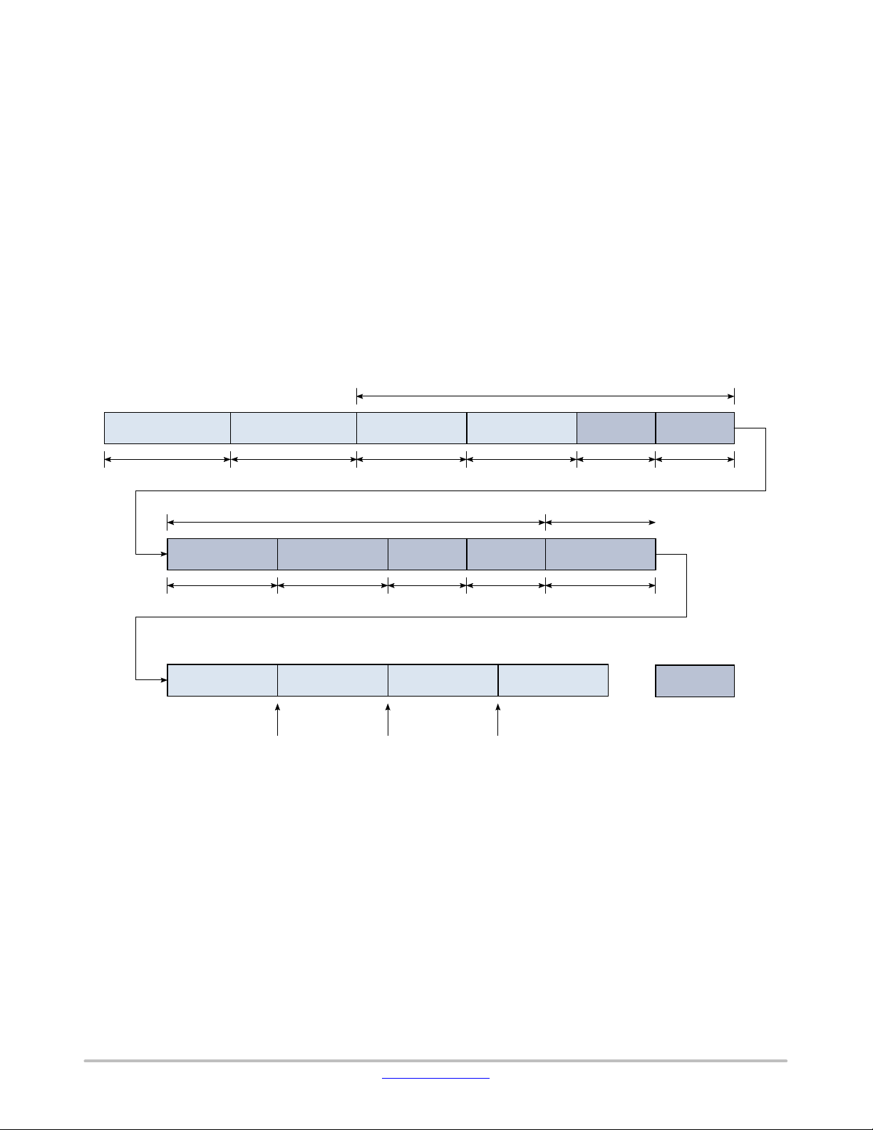
Figure 12 shows the receiver timing diagram. The actions
in the first two lines are time controlled. The arrows below
indicate which register controls the timing. The actions
colored in a darker shade of blue are only performed when
diversity mode is enabled (DIVENA is set in register
DIVERSITY). The actions in the last line are detailed in the
state diagram Figure 13.
SYNTHBOOST and SYNTHSETTLE form the two
stage procedure to settle the synthesizer on the first LO
frequency. During SYNTHBOOST, the synthesizer is
operated at a higher loop bandwidth (register
PLLLOOPBOOST), while during SYNTHSETTLE, the
final settling is done at the nominal, lower noise, loop
bandwidth (register PLLLOOP).
IFINIT settles the IF strip. COARSEAGC uses a fast AGC
time constant to quickly settle the AGC to a value close to
the correct one. This is especially important during
wake-on-radio, as it is desirable to keep the receiver
powered the shortest possible time to save power. AGC
settles the AGC using a slower time constant. RSSI
measures the received signal strength. This value is then
used to determine whether the receiver should be kept
running in wake-on-radio, or to select the antenna with the
stronger signal in diversity mode.
Antenna #0
SYNTHBOOST SYNTHSETTLE IFINIT COARSEAGC AGC RSSI
TMGRXBOOST TMGRXSETTLE TMGRXOFFSACQ TMGRXCOARSEAGC TMGRXAGC TMGRXRSSI
Antenna #1 Selected Antenna
IFINIT COARSEAGC AGC RSSI IFINIT
TMGRXOFFSACQ TMGRXCOARSEAGC TMGRXAGC TMGRXRSSI TMGRXOFFSACQ
PREAMBLE1 PREAMBLE2 PREAMBLE3 PACKET
MATCH0MATCH1 SFD detected
Figure 12. Receiver Flow Chart
Once the receiver is initialized, PREAMBLE1,
PREAMBLE2, PREAMBLE3, and PACKET coordinate
the reception of packets. The receiver contains several loops
that acquire and track transmission parameters the receiver
needs to know in order to correctly receive a packet.
• The AGC acquires and tracks the signal strength
• The frequency tracking loop acquires and tracks the
frequency offset
• The timing and data rate tracking loop acquires and
tracks the sampling time and the data rate offset
The bandwidth of these loops is programmable. The
bandwidth controls the acquisition time as well as the
Antenna
Diversity only
noisiness of the parameter estimates. In order to allow both
fast acquisition to enable short preambles and low steady
state noise performance to enable high receiver sensitivity,
the receiver supports multiple acquisition and tracking loop
parameter sets. When the receiver searches for a
transmission signal, it uses wide loop bandwidths. Once it
detects a preamble with sufficient probability, it switches to
a lower loop bandwidth. Once a frame start is detected, it
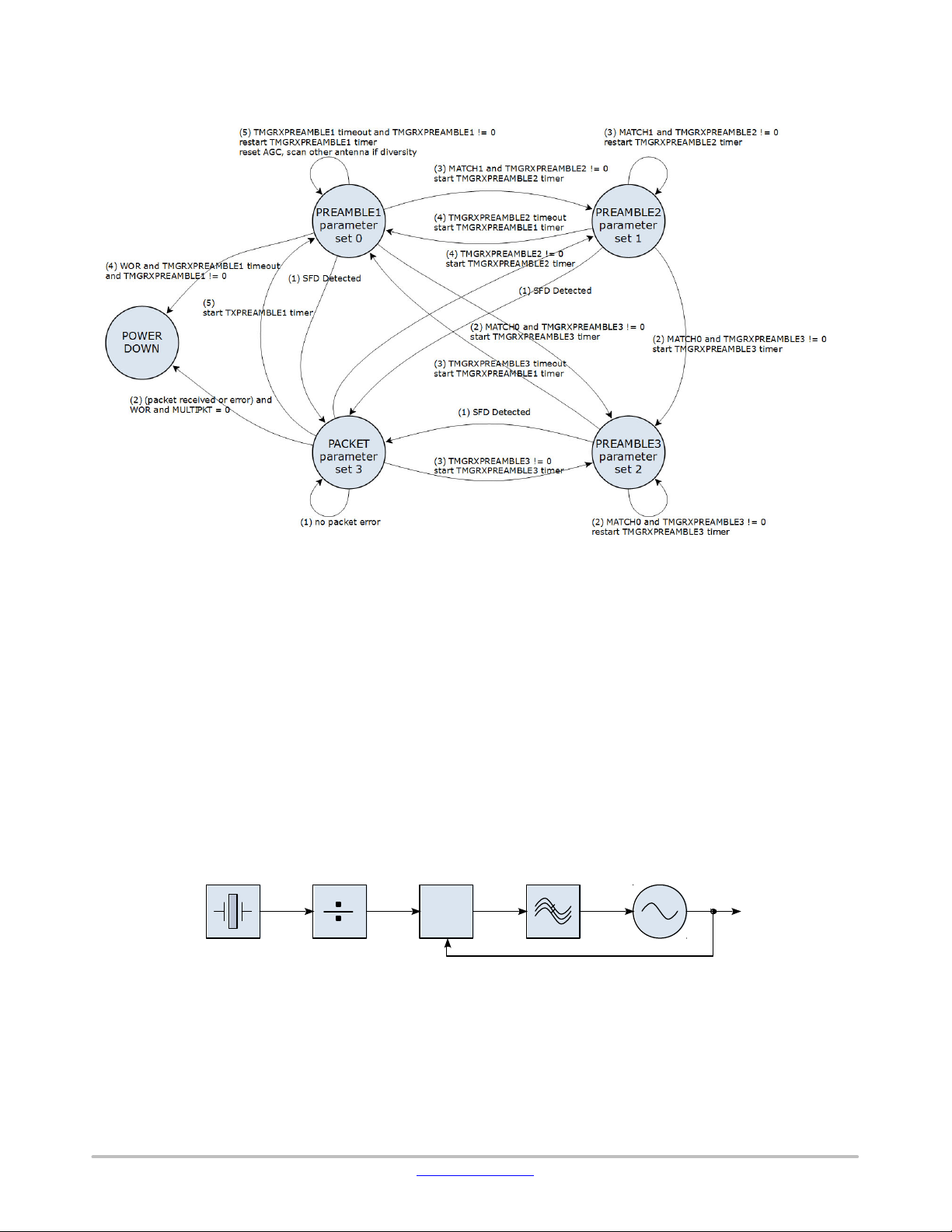
switches to an even lower loop bandwidth. Figure 13 shows
the state diagram that controls which receiver parameter set
is used.
www.onsemi.com
18
AND9902/D
Crystal
or TCXO
LPOSCREF
FD
LPOSCKFILT LPOSCFREQ
Figure 13. Receiver State Diagram
Conditions are evaluated in priority order. The priority
number is given in parentheses at the beginning of arrow
labels.
In order to reduce the number of registers that need to be
programmed if not all parameter sets are different, the
parameter set number of Figure 13 is not directly used to
address the parameter set. Instead, it indexes into register
RXPARAMSETS, where the actual parameter set number is
read out.
Low Power Oscillator Calibration
The low power oscillator is used to control the wake-up
frequency , o r polling period, during wake-on-radio mode. In
Figure 14. Low Power Oscillator Calibration Logic
order to increase the precision of the wake-up frequency,
calibration logic allows the low power oscillator to be
calibrated against the crystal oscillator or TCXO.
Figure 14 shows a block diagram of the calibration logic.
It works similarly to a PLL. The reference frequency from
the crystal or TCXO is divided by the value of the
LPOSCREF register. This signal is then compared to the
actual frequency of the Low Power Oscillator. The
frequency difference is then low pass filtered
(LPOSCKFILT register) and used to adjust the Low Power
Oscillator frequency (LPOSCFREQ register).
When enabled (LPOSCCALIBR or LPOSCCALIBF
enabled in register LPOSCCONFIG), the calibration logic
is only activated when the crystal oscillator or TCXO is
www.onsemi.com
enabled as well. This allows “opportunistic” calibration –
the Low Power Oscillator is calibrated whenever the
reference frequency is enabled.
19
AND9902/D
PWRAMP
or ANTSEL
R
C
GND
DAC Voltage
Auxiliary DAC
The AX5045 contains an auxiliary DAC. It can be used to
output various receiver signals, such as RSSI or Frequency
Offset, or just a value under program control. The DAC
signal can be output either on the PWRAMP or ANTSEL
pad.
The DAC may be operated in two modes. ΣΔ mode
employs a digital modulator to output a high resolution
signal. Its output voltage range is ¼ VDDIO to ¾ VDDIO
for a DACVALUE range from *2048 to 2047.
PWM mode outputs a pulse width modulated signal. It is
only suitable for low frequency signals. Its output voltage
range is 0 to VDDIO for a DACVALUE range from *2048
to 2047.
Figure 15. DAC RC Filter
A low pass filter, such as a simple R-C filter as shown in
Figure 15, must be used to obtain the analog voltage.
DACINPUT
0001
0010
0011
0100
0110
0111
1000
1001
1100
23 22 21 20 19 18 17 16 15 14 13 12 11 10 9 8 7 6 5 4 3 2 1 0
15
19
15
13
13
13
13
13
TRK_AMPLITUDE + 0x8000
TRK_RFFREQUENCY
TRK_FREQUENCY
TRK_FSKDEMOD
7
RSSI
0
0000 000000
SOFTDATA
I
Q
GPADC + 0x2000
0
00000000
0
0000
0
00000000
0
0000000000
000000
0
0
0
0
0000000000
0000000000
0000000000
0000000000
Shifter
register DACCONFIG selects the source signal. The input
signals are left aligned to 24 bits and padded with zeros. A
signed shifter then shifts the selected value to the right by 0
to 15 digits as selected by the lower four bits of the
DACVALUE register. The signal is then limited to the DAC
0000
Figure 16. DAC Signal Scaling
Figure 16 shows the DAC Signal scaling. DACINPUT in
www.onsemi.com
11
11
Limiter
DACVALUE
0
0
to DAC
value range of *2
11
to 211*1. This signal is then sent to the
DAC core. Note that if DACVALUE is selected as input, the
register value is directly sent to the DAC, the shifter is not
used. In fact, DACVALUE and DACSHIFT share the same
register bits.
20

REGISTER OVERVIEW
Table 23. CONTROL REGISTER MAP
Bit
7654321
0
Revision & Interface Probing
000
REVISION
RR01000110
SILICONREV(7:0)
Silicon Revision
001
SCRATCH
RWR11000101
SCRATCH(7:0)
Scratch Register
Operating Mode
002
PWRMODE
RWR000–0000
RST
XOEN
REFEN
WDS
PWRMODE(3:0)
Power Mode
Voltage Regulator
003
POWSTAT
RR––––––––
SSUM
SREF
SVREF
SVANA
SVMO
SBEVA
SBEVM
SVIO
Power
004
RR––––––––
SSSUM
SSREF
SSVRE
SSVANASSVM
SSBEV
SSBEV
SSVIO
Power
005
POWIRQMASK
RWR00000000
MPWR
MSREF
MSVREFMS
MSBE
MSBE
MSVIO
Power
Interrupt Control
006
IRQMASK1
RWR00000000
IRQMASK(15:8)
IRQ Mask
007
IRQMASK0
RWR00000000
IRQMASK(7:0)
IRQ Mask
009
RWR––000000
––RADIO EVENT MASK(5:0)
Radio Event
00A
IRQINVERSION1
RWR00000000
IRQINVERSION(15:8)
IRQ Inversion
00B
RWR00000000
IRQINVERSION(7:0)
IRQ Inversion
00C
IRQREQUEST1
RR––––––––
IRQREQUEST(15:8)
IRQ Request
00D
IRQREQUEST0
RR––––––––
IRQREQUEST(7:0)
IRQ Request
00F
R
––––––––
––RADIO EVENT REQ(5:0)
Radio Event
Modulation & Framing
010
MODULATION
RWR–––01000
–––
RX
MODULATION(3:0)
Modulation
011
ENCODING1
RWR–––––––0
–––––––
ENC
Encoder/Decod
012
ENCODING0
RWR00000100
ENC
ENC
ENC SCRPOLY(1:0)
ENC
ENC
ENC INV(1:0)
Encoder/Decod
013
FRAMING
RWR––––0000
FRMRX–––
FRMMODE(2:0)
FABOR
Framing settings
014
CRCCFG
RWR––––0000
––––CRCMODE(2:0)
CRCN
CRC settings
015
CRCINIT3
RWR11111111
CRCINIT(31:24)
CRC
016
CRCINIT2
RWR11111111
CRCINIT(23:16)
CRC
017
CRCINIT1
RWR11111111
CRCINIT(15:8)
CRC
018
CRCINIT0
RWR11111111
CRCINIT(7:0)
CRC
Forward Error Correction
019
FECRWR
00000000
SHOR
RSTVI
FEC
FEC
FECINPSHIFT(2:0)
FEC
FEC (Viterbi)
01A
FECSYNC
RWR01100010
FECSYNC(7:0)
Interleaver
01B
FECSTATUS
RR––––––––
FEC
MAXMETRIC(6:0)
FEC Status
AND9902/D
Addr Name Dir Ret Reset
POWSTICKYSTAT
RADIOEVENTMASK
IRQINVERSION0
RADIOEVENTREQ
GOOD
Description
DEM
F
VANAMSVMOD
ODEM
EM
NA
ANA
VANA
ODEM
MODEM
VMOD
EM
Management
Status
Management
Sticky Status
Management
Interrupt Mask
Mask
Request
ALTPN
9
T MEM
INV
SCRM
ODE
TERBI
NEG
HALF
SPEED
POS
MANC
H
DIFF
NOSY
NC
T
OINV
ENA
er Settings
er Settings
Initialization
Data
Initialization
Data
Initialization
Data
Initialization
Data
Configuration
Synchronization
Threshold
www.onsemi.com
21

AND9902/D
Status
01C
RADIOSTATE
R–––––0000
––––RADIOSTATE(3:0)
Radio Controller
01D
XTALSTATUS
RR––––––––
–––––––
XTAL
Crystal
Pin Configuration
020
PINSTATE
RR––––––––
––PS
PS
PS IRQ
PS
Pinstate
021
RWR1––00010
PU
––PFSYSCLK(4:0)
SYSCLK Pin
022
PINFUNCDCLK
RWR00–––100
PU
–––
PFDCLK(2:0)
DCLK Pin
023
PINFUNCDATA
RWR10–––111
PU
–––
PFDATA(2:0)
DATA Pin
024
PINFUNCIRQ
RWR00–––011
PU
PI IRQ–––PFIRQ(2:0)
IRQ Pin
025
RWR00–––110
PU
PI
–––
PFANTSEL(2:0)
ANTSEL Pin
026
RWR00––0110
PU
PI
––PFPWRAMP(3:0)
PWRAMP Pin
027
PWRAMP
RWR–––––––0
–––––––
PWRAMPPWRAMP
FIFO
028
FIFOSTAT
RR0–––––––
FIFO
–
FIFO
FIFO
FIFO
FIFO
FIFO
FIFO
FIFO Control
WRFIFOCMD(5:0)
029
FIFODATA
RW
––––––––
FIFODATA(7:0)
FIFO Data
02A
FIFOCOUNT1
RR–––––––0
–––––––
FIFO
Number of
02B
FIFOCOUNT0
RR00000000
FIFOCOUNT(7:0)
Number of
02C
FIFOFREE1
RR–––––––1
–––––––
FIFO
Number of
02D
FIFOFREE0
RR00000000
FIFOFREE(7:0)
Number of
02F
FIFOTHRESH
RWR00000000
FIFOTHRESH(7:0)
FIFO Threshold
Synthesizer
030
PLLLOOP
RWR0–––1001
FREQB–––
DIRECTFILTENFLT(1:0)
PLL Loop Filter
031
PLLCPI
RWR00001000
PLLCPI
PLL Charge
032
PLLRANGINGA1
RWR00000001
STICK
PLL
RNGERRRNG
STICK
VTUNE
–
VCOR
PLL
033
PLLRANGINGA0
RWR00000000
VCORA(7:0)
PLL
034
FREQA3
RWR00111001
FREQA(31:24)
Synthesizer
035
FREQA2
RWR00110100
FREQA(23:16)
Synthesizer
036
FREQA1
RWR11001100
FREQA(15:8)
Synthesizer
037
FREQA0
RWR11001101
FREQA(7:0)
Synthesizer
038
PLLLOOPBOOST
RWR0–––1011
FREQB–––
DIRECTFILTENFLT(1:0)
PLL Loop Filter
Table 23. CONTROL REGISTER MAP (continued)
Bit
Addr Description
ResetRetDirName
01234567
State
PINFUNCSYSCLK
PINFUNCANTSEL
PINFUNCPWRAMP
SYSCL
K
DCLKPIDCLK
DATAPIDATA
IRQ
ANTSE
L
PWRA
MP
AUTO
COMMI
T
ANTSE
L
PWRA
MP
PWR
AMP
FREE
THR
ANT
SEL
CNT
THR
OVER
RUN
DATAPSDCLKPSSYS
UNDE
R
FULL
CLK
EMPT
Y
COUN
T(8)
Oscillator Status
Function
Function
Function
Function
Function
Function
Control
Words currently
in FIFO
Y
LOCK
LOCK
START
Y
OFFR
NG
OFFR
NG
FREE(
8)
A(8)
Words currently
in FIFO
Words that can
be written to
FIFO
Words that can
be written to
FIFO
Settings
Pump Current
Autoranging
Autoranging
Frequency
Frequency
Frequency
Frequency
Settings
(Boosted)
www.onsemi.com
22

AND9902/D
039
PLLCPIBOOST
RWR11001000
PLLCPI
PLL Charge
03A
PLLRANGINGB1
RWR00000001
STICK
PLL
RNGERRRNG
STICK
VTUNE
–
VCOR
PLL
03B
PLLRANGINGB0
RWR00000000
VCORB(7:0)
PLL
03C
FREQB3
RWR00111001
FREQB(31:24)
Synthesizer
03D
FREQB2
RWR00110100
FREQB(23:16)
Synthesizer
03E
FREQB1
RWR11001100
FREQB(15:8)
Synthesizer
03F
FREQB0
RWR11001101
FREQB(7:0)
Synthesizer
040
PLLVCODIV
RWR–––00000
–––
RFDIV
REFDIV(1:0)
PLL Divider
Signal Strength
041
RSSIRR
––––––––
RSSI(7:0)
Received Signal
042
BGNDRSSI
RWR00000000
BGNDRSSI(7:0)
Background
043
DIVERSITY
RWR––––––00
––––––ANT
DIV
Antenna
044
AGCCOUNTER
RWR––––––––
AGCCOUNTER(7:0)
AGC Current
Receiver Tracking
045
TRKDATARATE2
RR––––––––
TRKDATARATE(23:16)
Datarate
046
TRKDATARATE1
RR––––––––
TRKDATARATE(15:8)
Datarate
047
TRKDATARATE0
RR––––––––
TRKDATARATE(7:0)
Datarate
048
TRKAMPL1
RR––––––––
TRKAMPL(15:8)
Amplitude
049
TRKAMPL0
RR––––––––
TRKAMPL(7:0)
Amplitude
04A
TRKPHASE1
RR––––––––
––––TRKPHASE(11:8)
Phase Tracking
04B
TRKPHASE0
RR––––––––
TRKPHASE(7:0)
Phase Tracking
04D
TRKRFFREQ2
RWR––––––––
––––TRKRFFREQ(19:16)
RF Frequency
04E
TRKRFFREQ1
RWR––––––––
TRKRFFREQ(15:8)
RF Frequency
04F
TRKRFFREQ0
RWR––––––––
TRKRFFREQ(7:0)
RF Frequency
050
TRKFREQ1
RWR––––––––
TRKFREQ(15:8)
Frequency
051
TRKFREQ0
RWR––––––––
TRKFREQ(7:0)
Frequency
052
TRKFSKDEMOD1
RR––––––––
––TRKFSKDEMOD(13:8)
FSK
053
TRKFSKDEMOD0
RR––––––––
TRKFSKDEMOD(7:0)
FSK
054
RR––––––––
TRKAFSKDEMOD(15:8)
AFSK
055
RR––––––––
TRKAFSKDEMOD(7:0)
AFSK
Timer
059
TIMER2
R–––––––––
TIMER(23:16)
1MHz Timer
05A
TIMER1
R–––––––––
TIMER(15:8)
1MHz Timer
05B
TIMER0
R–––––––––
TIMER(7:0)
1MHz Timer
Table 23. CONTROL REGISTER MAP (continued)
Bit
Addr Description
ResetRetDirName
01234567
Pump Current
(Boosted)
Y
LOCK
LOCK
START
Y
OFFR
NG
OFFR
NG
SEL
B(8)
ENA
Autoranging
Autoranging
Frequency
Frequency
Frequency
Frequency
Settings
Strength
Indicator
RSSI
Diversity
Configuration
Value
Tracking
Tracking
TRKAFSKDEMOD1
TRKAFSKDEMOD0
Tracking
Tracking
Tracking
Tracking
Tracking
Tracking
Tracking
Tracking
Demodulator
Tracking
Demodulator
Tracking
Demodulator
Tracking
Demodulator
Tracking
www.onsemi.com
23

AND9902/D
05C
TIMERCLK
RWR––––––10
––––––CLKMUX(1:0)
Internal Timer
Time Stamp
060
RWR00000000
RCTRLTIMESTAMP(23:16)
Radio Controller
061
RWR00000000
RCTRLTIMESTAMP(15:8)
Radio Controller
062
RWR00000000
RCTRLTIMESTAMP(7:0)
Radio Controller
064
RWR–––––––0
–––––––
TIMET
Radio Controller
Wakeup Timer
068
WAKEUPTIMER1
RR––––––––
WAKEUPTIMER(15:8)
Wakeup Timer
069
WAKEUPTIMER0
RR––––––––
WAKEUPTIMER(7:0)
Wakeup Timer
06A
WAKEUP1
RWR00000000
WAKEUP(15:8)
Wakeup Time
06B
WAKEUP0
RWR00000000
WAKEUP(7:0)
Wakeup Time
06C
WAKEUPFREQ1
RWR00000000
WAKEUPFREQ(15:8)
Wakeup
06D
WAKEUPFREQ0
RWR00000000
WAKEUPFREQ(7:0)
Wakeup
06E
RWR00000000
WAKEUPXOEARLY(7:0)
Wakeup Crystal
Physical Layer Parameters
Receiver Parameters
100
IFFREQ1
RWR00010011
IFFREQ(15:8)
2nd LO / IF
101
IFFREQ0
RWR00100111
IFFREQ(7:0)
2nd LO / IF
102
DECIMATION1
RWR––––––00
––––––DECIMATION(9:8)
Decimation
103
DECIMATION0
RWR00001101
DECIMATION(7:0)
Decimation
104
RXDATARATE2
RWR00000000
RXDATARATE(23:16)
Receiver
105
RXDATARATE1
RWR00111101
RXDATARATE(15:8)
Receiver
106
RXDATARATE0
RWR10001010
RXDATARATE(7:0)
Receiver
107
MAXDROFFSET2
RWR00000000
MAXDROFFSET(23:16)
Maximum
108
MAXDROFFSET1
RWR00000000
MAXDROFFSET(15:8)
Maximum
109
MAXDROFFSET0
RWR10011110
MAXDROFFSET(7:0)
Maximum
10A
MAXRFOFFSET2
RWR0–––0000
FREQ
–––
MAXRFOFFSET(19:16)
Maximum
10B
MAXRFOFFSET1
RWR00010110
MAXRFOFFSET(15:8)
Maximum
10C
MAXRFOFFSET0
RWR10000111
MAXRFOFFSET(7:0)
Maximum
10D
FSKDMAX1
RWR00000000
FSKDEVMAX(15:8)
Four FSK Rx
10E
FSKDMAX0
RWR10000000
FSKDEVMAX(7:0)
Four FSK Rx
10F
FSKDMIN1
RWR11111111
FSKDEVMIN(15:8)
Four FSK Rx
110
FSKDMIN0
RWR10000000
FSKDEVMIN(7:0)
Four FSK Rx
111
AFSKSPACE1
RWR––––0000
––––AFSKSPACE(11:8)
AFSK Space (0)
Table 23. CONTROL REGISTER MAP (continued)
Bit
Addr Description
ResetRetDirName
01234567
Clock Setting
RCTRLTIMESTAMP2
RCTRLTIMESTAMP1
RCTRLTIMESTAMP0
RCTRLTIMETXENA
WAKEUPXOEARLY
X ENA
Timestamp
Count
Timestamp
Count
Timestamp
Count
Timestamp
Enable
Frequency
Frequency
Oscillator Early
Frequency
Frequency
Factor
OFFS
CORR
Factor
Datarate
Datarate
Datarate
Receiver
Datarate Offset
Receiver
Datarate Offset
Receiver
Datarate Offset
Receiver RF
Offset
Receiver RF
Offset
Receiver RF
Offset
Deviation
Deviation
Deviation
Deviation
Frequency
www.onsemi.com
24

AND9902/D
112
AFSKSPACE0
RWR01000000
AFSKSPACE(7:0)
AFSK Space (0)
113
AFSKMARK1
RWR––––0000
––––AFSKMARK(11:8)
AFSK Mark (1)
114
AFSKMARK0
RWR01110101
AFSKMARK(7:0)
AFSK Mark (1)
115
AFSKCTRL
RWR–––00100
–––
AFSKSHIFT0(4:0)
AFSK Control
116
AMPLFILTER
RWR––––0000
––––AMPLFILTER(3:0)
Amplitude Filter
117
RWR00000000
ZIGZAGAMPLEXP(3:0)
ZIGZAGAMPLMANT(3:0)
RF Zigzag
118
RFZIGZAGFREQ
RWR00000000
ZIGZAGFREQ(7:0)
RF Zigzag
119
RWR–––
–––
RFFREQUENCYLEAK(4:0)
RF Frequency
11A
RWR0–––0000
PH
–––
FREQUENCYLEAK(3:0)
Baseband
11B
RXPARAMSETS
RWR00000000
RXPS3(1:0)
RXPS2(1:0)
RXPS1(1:0)
RXPS0(1:0)
Receiver
11C
RR––––––––
–––
RXSI(2)RXSN(1:0)
RXSI(1:0)
Receiver
11D
RWR00000000
RSSIIRQTHRESH(7:0)
RSSI Interrupt
11E
RSSIIRQDIR
RWR–––––––0
–––––––
RSSIII
RSSI Interrupt
F00
LNABIAS
RWR00000000
––––LNABIAS (3:0)
LNA Bias
F44
ADCDCCFG0
RWR00001111
––ADCS
––––−
For proper data
Receiver Parameter Set 0
120
AGCTARGET0
RWR10010110
AGCTARGET0(7:0)
AGC Target
121
RWR01011000
AGCDECAY0(4:0)
AGCMINDA0(2:0)
AGC Gain
122
AGCREDUCE0
RWR00100000
AGCATTACK0(4:0)
AGCMAXDA0(2:0)
AGC Gain
123
AGCAHYST0
RWR–––––000
–––––
AGCAHYST0(2:0)
AGC Digital
124
TIMEGAIN0
RWR11111000
TIMEGAIN0M(3:0)
TIMEGAIN0E(3:0)
Timing Gain
125
DRGAIN0
RWR11110010
DRGAIN0M(3:0)
DRGAIN0E(3:0)
Data Rate Gain
126
PHASEGAIN0
RWR11––0011
FILTERIDX0(1:0)
––PHASEGAIN0(3:0)
Filter Index,
127
FREQGAINA0
RWR00001111
FREQ
FREQ
FREQ
FREQ
FREQGAINA0(3:0)
Frequency Gain
128
FREQGAINB0
RWR00–11111
FREQ
FREQ
–
FREQGAINB0(4:0)
Frequency Gain
129
FREQGAINC0
RWR–––01010
–––
FREQGAINC0(4:0)
Frequency Gain
12A
FREQGAIND0
RWR00–01010
RFFRE
ZIGZA
–
FREQGAIND0(4:0)
Frequency Gain
12B
AMPLGAIN0
RWR010–0110
AMPL
AMPL
AMPL
–
AMPLGAIN0(3:0)
Amplitude Gain
Table 23. CONTROL REGISTER MAP (continued)
Bit
Addr Description
ResetRetDirName
01234567
Frequency
Frequency
Frequency
RFZIGZAGAMPL
RFFREQUENCYLEAK
FREQUENCYLEAK
RXPARAMCURSET
RSSIIRQTHRESH
00000
HALF
ACC
WAPIQ
RQ
DIR
Scanner
Amplitude
Exponent and
Mantissa
Scanner
Frequency
Recovery Loop
Leakiness
Frequency
Recovery Loop
Leakiness
Parameter Set
Indirection
Parameter
Current Set
Threshold
Threshold
Direction
(thermometer
encoded)
demodulation,
set bit 5 of this
register to 1.
Leave all other
bits as already
programmed.
AGCINCREASE0
LIM0
FREEZ
E0
Q
FREEZ
E0
AVG0
MODU
LO0
AVG0
G
FREEZ
E0
AGC0
www.onsemi.com
25
HALFM
OD0
HS0
AMPL
GATE0
Increase
Settings
Reduce Settings
Threshold
Range
Phase Gain
A
B
C
D
 Loading...