

Page 1

AND8084/D
NCP1650 Benchtop
Assistance
Prepared by: Alan Ball
ON Semiconductor
Applications Engineer
http://onsemi.com
APPLICATION NOTE
The NCP1650 is a high–performance, Power Factor
Correction IC. It is capable of producing a high power factor
input current waveform under continuous and discontinuous
modes of operation. It is also a highly integrated device,
and as such, requires fine tuning for optimum performance.
The purpose of this application note is to assist in
troubleshooting and fine tuning this circuit.
Troubleshooting
When troubleshooting this circuit, always use an
oscilloscope. DVM readings will not show oscillations,
spikes or other waveforms that may be helpful in
determining the cause of the problem.
Be aware that this is a non–isolated power converter that
is connected to a high–voltage, AC line. The ground of this
circuit will be at an AC potential and could pose a shock
hazard. Use an approved isolation transformer before
connecting oscilloscopes or other test equipment to this
circuit.
Output Does Not Regulate
1. High Output Voltage If the output voltage is greater
than 8% of the level of the designed output voltage,
check the voltage divider from the output to pin 6.
Make sure that the resistor values are correct, and
that the resistors are connected properly.
2. High Output Voltage
approximately 8% above the designed output level,
the overvoltage comparator is controlling the loop.
The switching will be erratic as the overvoltage
comparator inhibits the operation of the loop.
The input to the error amplifier (pin 6) should be 4.3 volts
under this condition. T he o utput o f t he e rror a mplifier ( pin 7)
should be high (approximately 6.0 volts). If it is not high,
check connections to this node.
The voltage/power OR’ing network inverts this signal,
which should cause the output of the reference multiplier
(pin 4) to be approximately zero volts.
The averaged current signal on pin 10 of the current sense
amplifier should be less than the output of the reference
multiplier on pin 4.
If the output voltage is
3. Low Output Voltage
than the designed output level, check the values in
the output voltage divider that connects to pin 6 of
the IC.
If the voltage divider values are correct, check the output
of the power error amplifier at pin 8. If this voltage level is
higher than the output of the voltage error amplifier (pin 7),
the power circuit is limiting the output. Check to make sure
that the load is within the rated range, and that the values of
R10, R9, and the current shunt are correct.
Unit Does Not Start
1. Typically, the inability of this unit to start–up is due
to inadequate Vcc. The NCP1650 requires a
minimum of 10.5 volts to turn on, and 9.5 to maintain
operation. If the Vcc voltage drops below 9.5 volts,
the chip will shut down.
When the chip begins operation, the bias current will
increase from a level of 0.5 mA to about 5.0 mA. Depending
on the start–up circuit used, there may not be enough energy
available to get the unit started before the Vcc drops below
9.5 volts.
In this case, a higher value Vcc cap may solve the
problem, and/or a higher current start–up circuit.
If the start–up circuit is operating properly, check the
voltage on pin 6. This pin has a shutdown feature that
requires a voltage of greater than 0.75 volts for the chip to
come out of its shutdown mode and commence operation.
Failure of Power Switch or High Voltage Diode
Overheating is the main cause of failures of these devices.
The rectifier diode will experience significant heating due to
the reverse recovery spike (unless a special circuit is used to
reduce this effect). Measure the temperature of the package
of both of these devices with a thermocouple and assure that
they do not exceed the manufacturers ratings. Additional
heatsinking and/or alternative parts may be required to keep
the temperature in a safe range.
The power switch has several protection circuits within
the NCP1650 controller. The main one being the
instantaneous current limit. If peak current is a concern,
check the values per the Excel spreadsheet or review the
design equations in the data sheet.
If the output voltage is less
Semiconductor Components Industries, LLC, 2002
May, 2002 – Rev. 0
1 Publication Order Number:
AND8084/D
Page 2
AND8084/D
The voltage on the power switch will exceed the output
voltage by a diode drop plus any spikes that may occur. A
good layout will keep these spikes to a minimum. Observe
the drain pin of the power switch with a wide bandwidth
oscilloscope to look for spikes. Spikes can be reduced by
adding snubbers or modifying the layout to reduce path
lengths between the inductor, drain and rectifier anode.
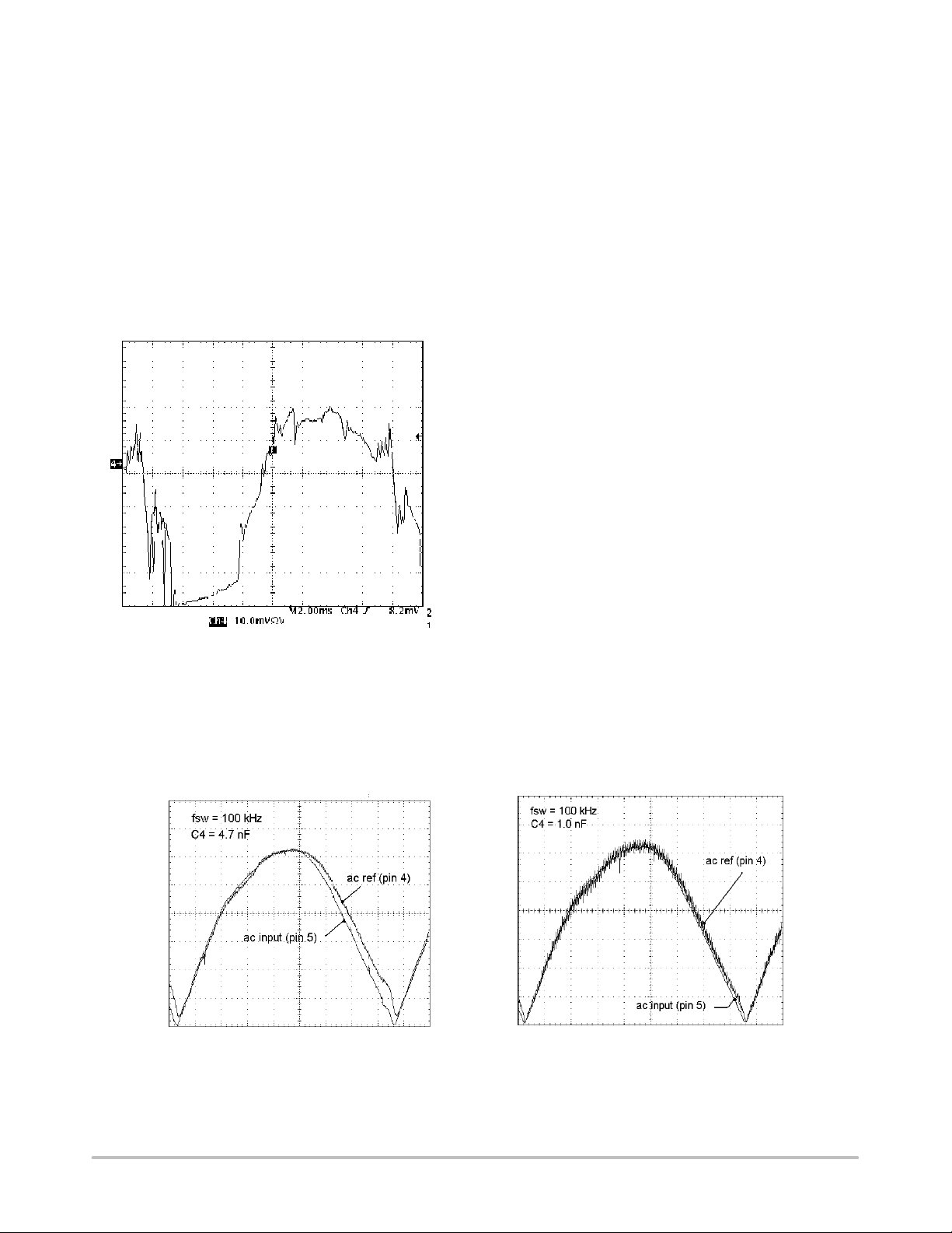
Noise Problems
Noise issues can be identified by abrupt changes in the
current waveform. Instabilities will cause smooth
oscillations, but noise will cause sharp edges as the current
steps from one level to another.
Figure 1. Example of Input Current Waveform
Distortion Due to Noise Issues
Possible causes are:
1. Poor grounding. In general, one of two grounding
schemes should be used.
• Single Point Ground – This is sometimes referred
to as a “star ground”. All major power traces should
be routed as closes as possible to a single point, and
routed directly to that point. This includes the shunt
resistor, FET source, output capacitor, input bypass
capacitor, and one trace going to all signal circuitry.
The chip ground should be as close as possible to the
ground side of the shunt resistor.
• Ground Plane – One layer of the printed circuit
board is left as a solid copper plane and all grounds
are connected to this plane. Even with a ground
plane, it is recommended to keep the high power
grounds (as described in the above paragraph) close
to each other, as well as keeping the chip ground
close to the current shunt resistor ground.
2. Reduce rise and fall times of the power device.
Increasing the resistance in the gate lead of the power
FET will reduce the speed of its transitions. This will
result in increased switching losses in the power
switch. Snubber circuits can be added across the FET
and/or diode to reduce noise levels. There are several
types of snubbers including RC and RCD
configurations.
3. Noise can also be radiated from various sources. The
node of the FET drain, output rectifier, and boost
inductor is a very noisy source, with both high
voltages and high dv/dt’s. Sensitive components,
which include most bias components of the
NCP1650, should be kept away from this node.
Traces between these components should be kept as
short as possible to reduce these emissions.
Performance
Figure 2. AC Ref with Phase Delay Figure 3. AC Ref with Minimal Phase Delay
http://onsemi.com
2
Page 3

AND8084/D
How to Improve Harmonics and Distortion
Low harmonic content and distortion are achieved by
forcing the input current to exactly replicate the waveshape
of the input voltage. To do this the output of the reference
multiplier must be an accurate copy of the input haversine
waveform. It is the function of the AC error amplifier loop
to force the input current to copy this waveform. This loop
includes the current sense amplifier averaged output, the AC
error amplifier, and the output of the reference multiplier.
1. Check output of reference multiplier. With an
oscilloscope, view the waveshape on pins 4 and 5.
Pin 4 should copy the waveshape of pin 5. If not,
confirm that the AC input (pin 5) does not exceed
4 volts peak, and check the output of the voltage
error amplifier per the next step. The waveform on
pin 5 (AC input) should be a scaled version of the
input haversine after the rectifiers. If it is shifted in
phase or does not go to zero, the cap on pin 5 should
be reduced in value. Decreasing the value on pin 5
will reduce errors in the reference signal, but also
increase the AC ripple (see Figures 2 and 3).
2. Check output of voltage error amplifier. It should be
a DC signal. If there is much ripple on it, recheck
calculations and components for the compensation
network of C7 and R7. If the ripple is random, it
could be a noise problem. Check grounding and
proximity to high frequency, high voltage/current
nodes. If the ripple is at the line frequency reduce
loop bandwidth by modifying compensation
components on pin 7. It is often helpful to add a small
bypass capacitor to this point. Start with a value that
is 1/100
3. Check average current signal on pins 10 and 11.
There should be a small amount of switching
frequency ripple (up to several hundred millivolts).
If other frequencies are noted determine if it is a
constant frequency. Random spacing of peaks
indicates noise, repeatable spacing indicates an
oscillation. If circuit is oscillating, reduce value of
R3 and increase C3 by the same percentage.
4. If the voltage error amplifier and average current
signal are both good, harmonics may be reduced by
increasing the bandwidth of the AC error amplifier.
To do this decrease the value of C3. Be cautious
when doing so, to maintain loop stability. If there are
oscillations on pins 10 and 11 (see Figure 4), reduce
the gain of the current shaping loop by decreasing the
value of R3 and increasing the value of C3 by the
same percentage.
th
of the value of C7.
Figure 4. Current Shaping Loop Oscillations
Poor Power Factor
Poor power factor is caused by two phenomena. One is the
distortion of the input current waveform, relative to the input
voltage waveform. The other is the phase shift of the input
current waveform. Improving the harmonics and THD will
improve the power factor due to distortion issues. The input
EMI filter can cause poor power factor due to its
capacitance, especially at high line.
The reason that the power factor suffers at high line is the
phase shift due to the combination of the input current to the
converter, and the current in the EMI capacitors. The input
current to the converter reduces at high line, due to the fact
that the unit is essentially a constant power device and as the
line voltage increases, the line current must decrease
proportionally. The capacitor current increases at high line
due to the increased voltage on the capacitors. The following
example illustrates this point.
For a 1000 watt unit, with an efficiency of 95%, and an
input voltage range of 85 to 265 volts, the input current
would be:
Iin
= 1000 w/(85 v x .95) = 12.4 amps
low
Iin
= 1000 w/(265 v x .95) = 3.97 amps
high
This current is in phase with the input voltage.
If we assume a total input capacitance of 8.0 F, and a line
frequency of 60 Hz, the reactive current is:
Iz
= 85 v x 2 x p x 60 Hz x 8.0 F = .26 amps
low
http://onsemi.com
3
Page 4

Iz
= 265 v x 2 x p x 60 Hz x 8.0 F = .80 amps
high
AND8084/D
I
pk
The power factor due to the phase displacement is:
Q
= arctan (.26/12.4) = 1.20°
low
PF
= cos Q = 1.00
low
Q
= arctan (.80/3.97) = 11.4°
high
PF
= cos Q = .980
high
It is recommended that the AC caps be kept as small as
possible, while still assuring proper operation, as well as
meeting the EMI specifications. One criteria to consider is
the value of the capacitance on the AC side of the line vs. the
value on the rectified side.
The capacitor on the rectified side of the line, will have a
DC component associated with it. It should also carry the
majority of the high frequency switching current, as
opposed to requiring it to flow through the rectifiers.
A good starting point is to calculate the allowable
high–frequency voltage ripple for this capacitor. The input
current will normally be in the continuous conduction mode
of operation at low line and full load. The ripple on the input
filter capacitor due to this waveform is:
I
C
I
t
on
t
off
T
min
V
C
Figure 5. Input Capacitor Voltage
and Current Waveforms
I
V
c
8·C
T
Where:
Vc is the capacitor peak–to–peak voltage in volts
I is the peak–to–peak ripple current. This can be found on
sheet 1 of the NCP1650 design spreadsheet in the “P–P
Ripple Current vs. Angle” graph.
T is the switching period in seconds
C is the capacitance in Farads
The capacitor on the AC side of the line should be at least
a factor of 2 greater than the capacitor on the rectified side
of the line and typically a factor of 5 or more. The capacitor
on the rectified side of the line will tend to hold up the
voltage at zero crossings, and will contribute to the
distortion in the current waveform, whereas, the capacitor
on the AC side of the line will help to filter any distortion at
the zero crossings, but will cause phase shift.
ON Semiconductor and are registered trademarks of Semiconductor Components Industries, LLC (SCILLC). SCILLC reserves the right to make
changes without further notice to any products herein. SCILLC makes no warranty, representation or guarantee regarding the suitability of its products for any
particular purpose, nor does SCILLC assume any liability arising out of the application or use of any product or circuit, and specifically disclaims any and all
liability, including without limitation special, consequential or incidental damages. “Typical” parameters which may be provided in SCILLC data sheets and/or
specifications can and do vary in different applications and actual performance may vary over time. All operating parameters, including “Typicals” must be
validated for each customer application by customer’s technical experts. SCILLC does not convey any license under its patent rights nor the rights of others.
SCILLC products are not designed, intended, or authorized for use as components in systems intended for surgical implant into the body, or other applications
intended to support or sustain life, or for any other application in which the failure of the SCILLC product could create a situation where personal injury or death
may occur. Should Buyer purchase or use SCILLC products for any such unintended or unauthorized application, Buyer shall indemnify and hold SCILLC
and its officers, employees, subsidiaries, affiliates, and distributors harmless against all claims, costs, damages, and expenses, and reasonable attorney fees
arising out of, directly or indirectly, any claim of personal injury or death associated with such unintended or unauthorized use, even if such claim alleges that
SCILLC was negligent regarding the design or manufacture of the part. SCILLC is an Equal Opportunity/Affirmative Action Employer.
PUBLICATION ORDERING INFORMATION
Literature Fulfillment:
Literature Distribution Center for ON Semiconductor
P.O. Box 5163, Denver, Colorado 80217 USA
Phone: 303–675–2175 or 800–344–3860 Toll Free USA/Canada
Fax: 303–675–2176 or 800–344–3867 Toll Free USA/Canada
Email: ONlit@hibbertco.com
N. American Technical Support: 800–282–9855 Toll Free USA/Canada
http://onsemi.com
JAPAN: ON Semiconductor, Japan Customer Focus Center
4–32–1 Nishi–Gotanda, Shinagawa–ku, Tokyo, Japan 141–0031
Phone: 81–3–5740–2700
Email: r14525@onsemi.com
ON Semiconductor Website: http://onsemi.com
For additional information, please contact your local
Sales Representative.
AND8084/D
4
 Loading...