

ON Semiconductor ADP3212, NCP3218 Datasheet

7-Bit Programmable,
S
3-Phase, Mobile CPU
ynchronous Buck
Controller
FEATURES
Single-chip solution
Fully compatible with the Intel® IMVP-6.5™ specifications
Selectable 1- , 2-, or 3-phase operation with up to 1 MHz per
phase switching frequency
Phase 1 and Phase 2 Integrated MOSFET drivers
Input Voltage Range of 3.3 V to 22 V
Guaranteed ±8 mV worst-case differentially sensed core
voltage error over temperature
Automatic power-saving mode maximizes efficiency with
light load during deeper sleep operation
Active current balancing between output phases
Independent current limit and load line setting inputs for
additional design flexibility
Built-in power-good blanking supports
voltage identification (VID) on-the-fly transients
7-bit, digitally programmable DAC with 0.3 V to 1.5 V output
Short-circuit protection with programmable latch-off delay
Clock enable output delays the CPU clock until the core
voltage is stable
Output power or current monitor options
48-lead QFN 6x6mm (NCP3218)
48-lead QFN 7x7mm (ADP3212)
APPLICATIONS
Notebook power supplies for next-generation Intel processors
ADP3212/NCP3218
GENERAL DESCRIPTION
The ADP3212/NCP3218 is a highly efficient, multiphase,
synchronous buck switching regulator controller. With its
integrated drivers, the ADP3212/NCP3218 is optimized for
converting the notebook battery voltage into the core supply
voltage required by high performance Intel processors. An internal
7-bit DAC is used to read a VID code directly from the processor
and to set the CPU core voltage to a value within the range of
0.3 V to 1.5 V. The ADP3212/NCP3218 is programmable for 1-,
2-, or 3-phase operation. The output signals ensure interleaved
2- or 3-phase operation.
The ADP3212/NCP3218 uses a multimode architecture run at a
programmable switching frequency and optimized for efficiency
depending on the output current requirement. The
ADP3212/NCP3218 switches between single- and multi-phase
operation to maximize efficiency with all load conditions. The chip
includes a programmable load line slope function to adjust the
output voltage as a function of the load current so that the core
voltage is always optimally positioned for a load transient. The
ADP3212/NCP3218 also provides accurate and reliable shortcircuit protection, adjustable current limiting, and a delayed
power-good output. The IC supports on-the-fly output voltage
changes requested by the CPU.
The ADP3212/NCP3218 are specified over the extended
commercial temperature range of -40°C to 100°C. The ADP3212
is available in a 48-lead QFN 7x7mm 0.5 mm pitch package.
The NCP3218 is available in a 48-lead QFN 6x6mm 0.4 mm
pitch package. Except for the packages, the ADP3212 and
NCP3218 are identical. ADP3212 and NCP3218 are HalogenFree, Pb-Free and RoHS compliant.
Rev. SpA | Page 1 of 43
ADP3212/NCP3218
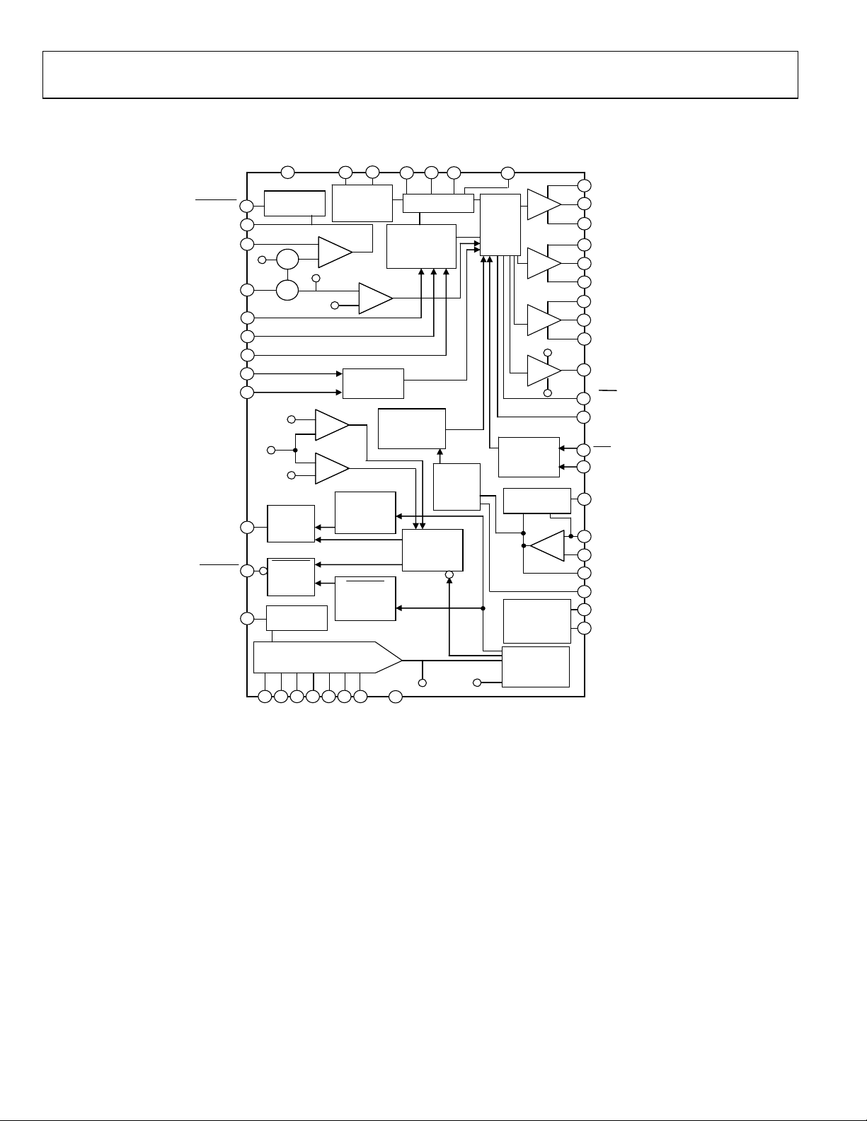
FUNCTIONAL BLOCK DIAGRAM
ENGND
VCC
RPM RT RAMP
VARFREQ
TRDETTRDET
COMP
FB
LLINE
SWFB1
SWFB2
SWFB3
PH0
PH1
PWRGD
CLKENCLKEN
FBRTN
TRDET
TRDET
Generator
Generator
+
ΣΣ
REF
DAC + 200mV
DAC - 300mV
+
CSREF
PWRGD
Open
Drain
CLKEN
CLKEN
Open
Open
Drain
Drain
Precision
Precision
Reference
Reference
+
ΣΣ
_
1.55V
VID
DAC
Shutdown
Shutdown
VEA
-
+-+
CSREF
-
+-+
-
+-+
UVLO
UVLO
and Bias
and Bias
OVP
+-+
-
Number of
Phases
PWRGD
Start Up
Delay
CLKEN
CLKEN
Start Up
Start Up
Delay
Delay
Oscillator
Current
Current
Balancing
Balancing
Circuit
Circuit
OCP
Shutdown
Delay
Soft
Transient
Delay
Delay
Disable
DAC
Current
Limit
Circuit
REF
Driver
Logic
PSI and
PSI and
DPRSLP
DPRSLP
Logic
Logic
Current
Current
Monitor
Monitor
Thermal
Thermal
Throttle
Throttle
Control
Control
Soft Start
PVCC
PGND
+
-+-
BST1
DRVH1
SW1
PVCC
DRVL1
PGND
BST2
DRVH2
SW2
DRVL2
OD3OD3
PWM3
PSIPSI
DPRSLP
IMON
CSREF
CSSUM
CSCOMP
ILIM
TTSENSE
VRTT
VID6
VID5
VID4
VID3
VID2
VID1
VID0
IREF
Figure 1.
Rev. SpA | Page 2 of 43

ADP3212/NCP3218
TABLE OF CONTENTS
Features...............................................................................................1
Applications .......................................................................................1
General Description..........................................................................1
Functional Block Diagram...............................................................2
Revision History................................................................................3
Specifications .....................................................................................4
Timing Diagram................................................................................9
Absolute Maximum Ratings ..........................................................10
ESD Caution ................................................................................10
Pin Configuration and Function Descriptions ...........................11
Test Circuits .....................................................................................13
Typical Performance Characteristics............................................14
Theory of Operation.......................................................................15
Number of Phases .......................................................................15
Operation Modes ........................................................................15
Differential Sensing of Output Voltage....................................19
Output Current Sensing .............................................................19
Active Impedance Control Mode..............................................19
Current Control Mode and Thermal Balance.........................20
Voltage Control Mode................................................................20
Power-Good Monitoring............................................................20
Power-Up Sequence and Soft Start ...........................................21
Current Limit...............................................................................21
Output Crowbar..........................................................................24
Reverse Voltage Protection........................................................24
Output Enable and UVLO.........................................................24
Thermal Throttling Control......................................................24
Application Information ................................................................28
Setting the Clock Frequency for PWM....................................28
Setting the Switching Frequency for RPM Operation of Phase
1 .....................................................................................................28
Soft Start and Current Limit Latch-Off Delay Times ............28
Inductor Selection.......................................................................28
C
Selection..............................................................................31
OUT
Power MOSFETs.........................................................................32
Ramp Resistor Selection.............................................................33
Current Limit Setpoint...............................................................33
Current Monitor..........................................................................33
Feedback Loop Compensation Design ....................................33
CIN Selection and Input Current di/dt Reduction ..................35
RC Snubber..................................................................................35
Selecting Thermal Monitor Components................................35
Tuning Procedure for ADP3212/NCP3218.............................36
Layout and Component Placement ..........................................37
Outline Dimension .........................................................................39
Ordering Guide...........................................................................41
Changing VID on the Fly...........................................................21
REVISION HISTORY
4/08—Revision Sp0: Initial Version
Rev. SpA | Page 3 of 43

ADP3212/NCP3218
SPECIFICATIONS
VCC = PVCC = 5V, FBRTN = PGND = GND = 0 V, H = 5V, L = 0 V, EN = VARFREQ = H, DPRSLP = L,
1.2000 V, T
= −40°C to 100°C, unless otherwise noted.1 Current entering a pin (sink current) has a positive sign.
A
PSI
= 1.05 V, V
= VDAC =
VID
Table 1.
Parameter Symbol Conditions Min Typ Max Units
VOLTAGE CONTROL
VOLTAGE ERROR AMPLIFIER
(VEAMP)
FB, LLINE Voltage Range2 V
FB, LLINE Offset Voltage2 V
LLINE Bias Current I
FB Bias Current IFB −1 +1
LLINE Positioning Accuracy VFB − V
, V
Relative to CSREF = VDAC −200 +200 mV
FB
LLINE
Relative to CSREF = VDAC −0.5 +0.5 mV
OSVEA
−100 +100 nA
LLINE
Measured on FB relative to V
VID
, LLINE forced 80 mV
VID
−77.5 −80 −82.5 mV
μA
below CSREF
COMP Voltage Range2 V
COMP Current
COMP Slew Rate SR
Gain Bandwidth2 GBW Non-inverting unit gain configuration, RFB = 1
0.85 4.0 V
COMP
I
COMP
C
COMP
COMP = 2 V, CSREF = VDAC
FB forced 200 mV below CSREF
FB forced 200 mV above CSREF
= 10 pF, CSREF = VDAC, Open loop
COMP
configuration
FB forced 200 mV below CSREF
FB forced 200 mV above CSREF
−0.75
6
15
-20
20 MHz
mA
mA
V/μs
V/μs
kOhm
VID DAC VOLTAGE REFERENCE
VDAC Voltage Range2 See VID table 0 1.5 V
VDAC Accuracy VFB − V
VDAC Differential
−1 +1 LSB
VID
Measured on FB (includes offset), relative to V
= 1.2000 V to 1.5000 V, T = −40C to 100C
V
VID
V
= 0.3000 V to 1.1875 V, T = −40C to 100C
VID
VID
−8.5
−7.5
+8.5
+7.5
mV
mV
Nonlinearity2
VDAC Line Regulation
VDAC Boot Voltage V
Soft-start Delay
2
ΔV
FB
BOOTFB
t
Measured from EN pos edge to FB = 50 mV 200
DSS
Soft-start Time tSS Measured from FB = 50 mV to FB settles to 1.1 V
VCC = 4.75 V to 5.25 V 0.02 %
Measured during boot delay period 1.100 V
μs
1.4 ms
within 5 %
Boot Delay t
Measured from FB settling to 1.1 V within 5% to
BOOT
60
μs
CLKEN# neg edge
VDAC Slew Rate2 Soft-start
Non-LSB VID step, DPRSLP = H, Slow C4 Entry/Exit
Non-LSB VID step, DPRSLP = L, Fast C4 Exit
LSB VID step, DVID transition
FBRTN Current I
VOLTAGE MONITORING
−90 −200
FBRTN
0.0625
0.25
1
0.4
LSB/μs
LSB/μs
LSB/μs
LSB/μs
μA
and PROTECTION
POWER GOOD
CSREF Under-voltage
Threshold
CSREF Over-voltage
Threshold
V
Relative to nominal VDAC voltage −240 −300 −360 mV
UVCSREF
V
Relative to nominal VDAC voltage 150 200
OVCSREF
250 mV
Rev. SpA | Page 4 of 43

ADP3212/NCP3218
Parameter Symbol Conditions Min Typ Max Units
CSREF Crowbar Voltage
Threshold
CSREF Reverse Voltage
Threshold
PWRGD Low Voltage V
PWRGD High, Leakage
Current
PWRGD Start-up Delay T
PWRGD Latch-off Delay T
PWRGD Propagation Delay3 T
Crowbar Latch-off Delay2 T
PWRGD Masking Time Triggered by any VID change or OCP event 100 s
CSREF Soft-stop Resistance EN = L or Latch-off condition 70
CURRENT CONTROL
CURRENT-SENSE AMPLIFIER
(CSAMP)
CSSUM, CSREF Common-
Mode Range2
CSSUM, CSREF Offset Voltage V
CSSUM Bias Current I
CSREF Bias Current I
CSCOMP Voltage Range2 Voltage range of interest 0.05 2 V
CSCOMP Current
CSCOMP Slew Rate2 C
Gain Bandwidth2 GBW
CURRENT MONITORING
and PROTECTION
CURRENT REFERENCE
IREF Voltage V
CURRENT LIMITER (OCP)
Current Limit (OCP)
Threshold
Current Limit Latch-off Delay Measured from OCP event to PWRGD de-assertion 120 s
CURRENT MONITOR
Current Gain Accuracy I
V
Relative to FBRTN, V
CBCSREF
Relative to FBRTN, V
V
RVCSREF
Relative to FBRTN, Latch-off mode
CSREF is falling
CSREF is rising
I
PWRGD
I
V
PWRGD
SSPWRGD
PWRGD(SINK)
PWRDG
Measured from CLKEN# neg edge to PWRGD pos
= 4 mA 85 250 mV
= 5 V 1 A
> 1.1 V
VID
≤ 1.1 V
VID
1.5
1.3
−370 −300
1.55
1.35
−75
1.6
1.4 V V
−10
mV
mV
8 ms
edge
Measured from Out-off-Good-Window event to
LOFFPWRGD
120 s
Latch-off (switching stops)
PDPWRGD
Measured from Out-off-Good-Window event to
200 ns
PWRGD neg edge
LOFFCB
Measured from Crowbar event to Latch-off
200 ns
(switching stops)
Ω
Voltage range of interest 0 2 V
CSREF – CSSUM , TA = −40C to 85C −1.2 +1.2 mV
OSCSA
−20 +20 nA
BCSSUM
−3 +3
BCSREF
I
CSCOMPsource
I
CSCOMPsink
CSCOMP = 2 V,
CSSUM forced 200 mV below CSREF
CSSUM forced 200 mV above CSREF
= 10 pF, CSREF = VDAC, Open loop
CSCOMP
configuration
CSSUM forced 200 mV below CSREF
−750
1
20
−20
μA
μA
mA
V/μs
V/μs
CSSUM forced 200 mV above CSREF
Non-inverting unit gain configuration
CSA
= 1 kOhm
R
FB
20 MHz
REF
R
= 80 kΩ to set I
REF
= 20 uA
REF
1.55 1.6 1.65 V
V
Measured from CSCOMP to CSREF, R
LIMTH
3-ph configuration,
3-ph configuration,
2-ph configuration,
2-ph configuration,
1-ph configuration −75 −90 −106 mV
PSI
PSI
PSI
PSI
= H
= L
= H
= L
= 1.5 kΩ,
LIM
−75
−22
−75
−36
−90
−30
−90
−45
−106
−38
−106
−54
mV
mV
mV
Measured from ILIM to IMON
MON/ILIM
I
= −20 μA
LIM
I
= −10 μA
LIM
Rev. SpA | Page 5 of 43
3.7
3.6
4
4
4.3
4.4
-
-

ADP3212/NCP3218
Parameter Symbol Conditions Min Typ Max Units
I
= −5 μA
LIM
IMON Clamp Voltage V
PULSE WIDTH
Relative to FBRTN, ILIMP = −30 uA 1.0 1.15 V
MAXMON
MODULATOR
CLOCK OSCILLATOR
RT Voltage VRT
PWM Clock Frequency
f
Operation of interest 0.3 3 MHz
CLK
Range2
PWM Clock Frequency f
RAMP GENERATOR
RAMP Voltage V
RAMP Current Range2 I
T
CLK
EN = high, I
RAMP
EN = high 1 100
RAMP
EN = low, RAMP = 19 V −1 +1 µA
PWM COMPARATOR
PWM Comparator Offset2 V
RPM COMPARATOR
RPM Current I
RPM Comparator Offset2 V
EPWM CLOCK SYNC
V
OSRPM
RPM
V
OSRPM
Trigger Threshold2 Relative to COMP sampled T
TRDET#
Trigger Threshold2 Relative to COMP sampled T
TRDET# Low Voltage2 V
TRDET# Leakage Current I
SWITCH AMPLIFIER
SW Common Mode Range2 V
SWFB Input Resistance R
ZERO CURRENT SWITCHING
Logic low, I
LTR D E T
Logic high, V
HTRDET
SW(X)CM
SW(X)
COMPARATOR
SW ZCS Threshold V
Masked Off-Time t
SYSTEM I/O BUFFERS
DCM(SW1)
OFFMSKD
VID[6:0], DPRSLP, PSI# INPUTS
Input Voltage Refers to driving signal level
VARFREQ = high, R
= 125 kΩ, V
T
= 1.5000 V
VID
VARFREQ = low
See also V
= +25°C, V
A
RT(VVID
VID
) formula
= 1.2000 V
RT = 72 kΩ
R
= 120 kΩ
T
RT = 180 kΩ
= 60 µA
RAMP
EN = low
− V
RAMP
V
= 1.2 V, RT = 215 kΩ
VID
See also I
COMP
±3 mV
COMP
) formula
RPM(RT
− (1 + V
) ±3 mV
RPMTH
time earlier
CLK
3-phase configuration
2-phase configuration
1-phase configuration
time earlier
CLK
3-phase configuration
2-phase configuration
1-phase configuration
= 4mA 30 300 mV
TRDET#sink
= VCC 5 µA
TRDET#
Operation of interest for current sensing −600 +200 mV
SWX = 0 V, SWFB = 0 V 20 35 50 kΩ
DCM mode, DPRSLP = 3.3 V −3 mV
Measured from DRVH1 neg edge to DRVH1 pos
edge at max frequency of operation
Logic low
Logic high
Rev. SpA | Page 6 of 43
3.5 4 4.5 -
1.125
0.9
1100
700
500
0.9 1
1.25
1
1257
800
550
VIN
1.375
1.1 V V
1400
900
600
kHz
kHz
kHz
1.1 V
V
μA
−9
350
400
450
-450
-500
-600
μA
mV
mV
mV
mV
mV
mV
600 ns
0.7
0.3 V
V

ADP3212/NCP3218
Parameter Symbol Conditions Min Typ Max Units
Input Current V = 0.2 V
VID[6:0], DPRSLP (active pull down to GND)
PSI# (active pull-up to VCC)
VID Delay Time2 Any VID edge to FB change 10% 200 ns
VARFREQ
Input Voltage Refers to driving signal level
Logic low
Logic high
Input Current 1
EN INPUT
Input Voltage Refers to driving signal level
Logic low
Logic high
Input Current EN = L or EN = H (static)
0.8 V < EN < 1.6 V (during transition)
PH1, PH0 INPUTS
Input Voltage Refers to driving signal level
Logic low
Logic high
Input Current 1
OUTPUT
CLKEN
Output Low Voltage Logic low, I
Output High, Leakage
= 4 mA 60 200 mV
sink
Logic high, V
= VCC 1 µA
CLKEN
Current
PWM3, OD3 OUTPUTS
Output Voltage Logic low, I
THERMAL MONITORING
and PROTECTION
= 400 µA
SINK
Logic high, I
SOURCE
= −400 µA
TTSNS Voltage Range2 0 5 V
TTSNS Threshold VCC = 5 V, TTSNS is falling 2.45 2.5 2.55 V
TTSNS Hysteresis 95 mV
TTSNS Bias Current TTSNS = 2.6 V −2 2 µA
VRTT Output Voltage V
SUPPLY
Supply Voltage Range V
Logic low, I
VRTT
Logic high, I
VRTT(SINK)
VRTT(SOURCE)
= 400 µA
= −400 µA
CC
4.5 5.5 V
Supply Current EN = high 7 10 mA
EN = 0 V 10 150 µA
VCC OK Threshold V
VCC UVLO Threshold V
VCC is rising 4.4 4.5 V
CCOK
VCC is falling 4.0 4.15 V
CCUVLO
VCC Hysteresis2 150 mV
HIGH-SIDE MOSFET DRIVER
Pull-up Resistance, Sourcing
Pull-down Resistance,
3
Current
Sinking Current
3
Transition Times tr
tf
Dead Delay Times tpdh
DRVH,
BST = PVCC, CL = 3 nF, Figure 2 13 25 ns
DRVH
DRVH
BST = PVCC 1.8 3.3 Ω
BST = PVCC 1.0 2.0 Ω
BST = PVCC, CL = 3 nF, Figure 2 15 30 ns
BST = PVCC, Figure 2 15 30 40 ns
Rev. SpA | Page 7 of 43
−1
1
4
1.9
10
−70
4
4
4.5
10
5
10
5
μA
μA
0.7 V
V
μA
0.4 V
V
nA
μA
V
0.5
μA
100 mV
V
100 mV
V

ADP3212/NCP3218
Parameter Symbol Conditions Min Typ Max Units
BST Quiescent Current EN = L (Shutdown) 1 10 µA
EN = H, no switching 200 µA
LOW-SIDE MOSFET DRIVER
Pull-up Resistance, Sourcing
Pull-down Resistance,
3
Current
Sinking Current
3
Transition Times tr
tf
Propagation Delay Times tpdh
SW Transition Timeout t
SW Off Threshold V
PVCC Quiescent Current EN = L (Shutdown) 1 10 µA
EN = H, no switching 170 µA
BOOTSTRAP RECTIFIER
SWITCH
On Resistance
1
All limits at temperature extremes are guaranteed via correlation using standard statistical quality control (SQC).
2
Guaranteed by design or bench characterization, not production tested.
3
Based on bench characterization data.
3
DRVL
C
DRVL
DRVL
TOSW
OFFSW
1.7 2.8 Ω
0.8 1.7 Ω
CL = 3 nF, Figure 2 15 35 ns
= 3 nF, Figure 2 14 35 ns
L
CL = 3 nF, Figure 2 11 30 ns
DRVH = L, SW = 2.5 V 100 250 350 ns
2.5 V
EN = L or EN = H and DRVL = H 4 6 8 Ω
Rev. SpA | Page 8 of 43
ADP3212/NCP3218
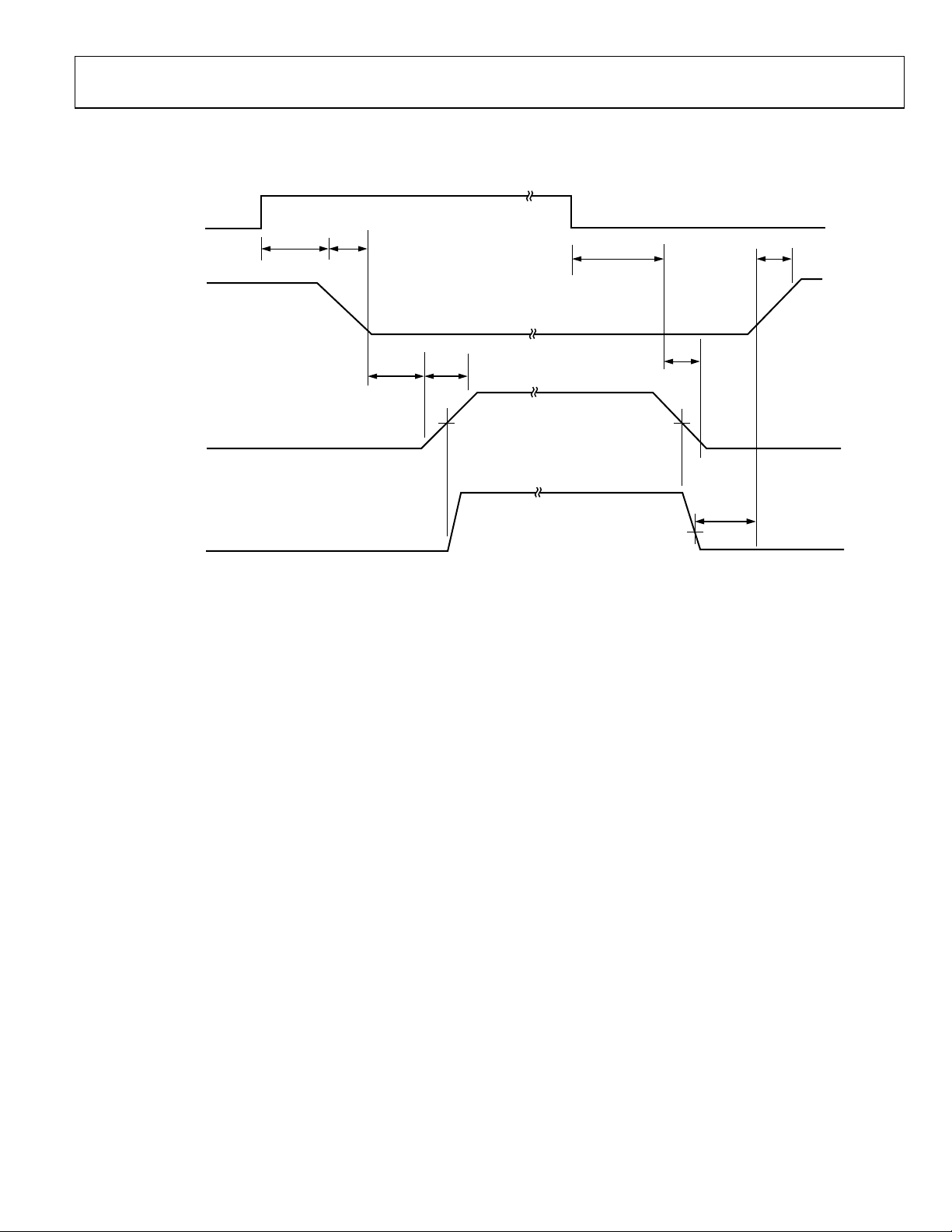
TIMING DIAGRAM
Timing is referenced to the 90% and 10% points, unless otherwise noted.
IN
DRVL
tf
DRVL
tpdh
DRVHtrDRVH
tpdl
DRVH
tf
DRVH
tr
DRVL
tpdl
DRVL
(WITH RESPECT
DRVH
TO SW)
SW
V
TH
Figure 2. Timing Diagram
V
TH
tpdh
DRVL
1V
06374-006
Rev. SpA | Page 9 of 43
ADP3212/NCP3218
ABSOLUTE MAXIMUM RATINGS
Table 2.
Parameter Rating
VCC, PVCC1, PVCC2 −0.3 V to +6 V
FBRTN, PGND1, PGND2 −0.3 V to +0.3 V
BST1, BST2, DRVH1, DRVH2
DC −0.3 V to +28 V
t < 200 ns −0.3 V to +33 V
BST1 to PVCC, BST2 to PVCC
DC −0.3 V to +22 V
t < 200 ns −0.3 V to +28 V
BST1 to SW1, BST2 to SW2 −0.3 V to +6 V
SW1, SW2
DC −1 V to +22 V
t < 200 ns −6 V to +28 V
DRVH1 to SW1, DRVH2 to SW2, −0.3 V to +6 V
DRVL1 to PGND1, DRVL2 to PGND2
DC −0.3 V to +6 V
t < 200 ns −5 V to +6 V
RAMP (in Shutdown) −0.3 V to +22 V
All Other Inputs and Outputs −0.3 V to +6 V
Storage Temperature −65°C to +150°C
Operating Ambient Temperature Range −40°C to 100°C
Operating Junction Temperature 125°C
Thermal Impedance (θJA) 2-Layer Board
Lead Temperature
Soldering (10 sec) 300°C
Infrared (15 sec) 260°C
30.5°C/W
Stresses above those listed under Absolute Maximum Ratings
may cause permanent damage to the device. This is a stress
rating only; functional operation of the device at these or any
other conditions above those indicated in the operational
section of this specification is not implied. Exposure to absolute
maximum rating conditions for extended periods may affect
device reliability.
ESD CAUTION
Rev. SpA | Page 10 of 43
ADP3212/NCP3218
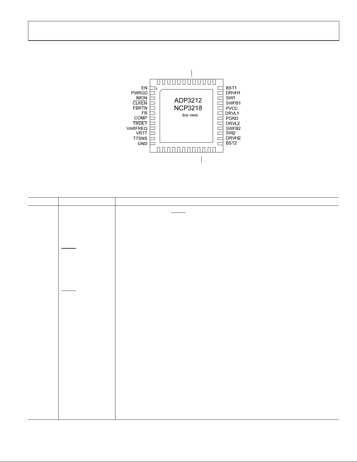
PIN CONFIGURATION AND FUNCTION DESCRIPTIONS
DPRSLP
ILIM
VCC
PH0
PH1
OD3
PWM3
SWFB3
VID0
RT
RPM
IREF
Figure 3. QFN Pin Configuration
LLINE
RAMP
VID6
CSREF
CSSUM
CSCOMP
PSI
VID5
VID4
VID3
VID2
VID1
Table 3. Pin Function Descriptions
Pin No. Mnemonic Description
1 EN Enable Input. Driving this pin low shuts down the chip, disables the driver outputs, pulls PWRGD
and VRTT low, and pulls
CLKEN
high.
2 PWRGD Power-Good Output. Open-drain output. A low logic state means that the output voltage is outside
of the VID DAC defined range.
3 IMON Current Monitor Output. This pin sources a current proportional to the output load current. A
resistor to FBRTN sets the current monitor gain.
4
CLKEN
Clock Enable Output. Open-drain output. A low logic state enables the CPU internal PLL clock to
lock to the external clock.
5 FBRTN Feedback Return Input/Output. This pin remotely senses the CPU core voltage. It is also used as the
ground return for the VID DAC and the voltage error amplifier blocks.
6 FB Voltage Error Amplifier Feedback Input. The inverting input of the voltage error amplifier.
7 COMP Voltage Error Amplifier Output and Frequency Compensation Point.
8
TRDET
Transient Detect Output. This pin is pulled low when a load release transient is detected. During
repetitive load transients at high frequencies, this circuit optimally positions the maximum and
minimum output voltage into a specified loadline window.
9 VARFREQ Variable Frequency Enable Input. A high logic state enables the PWM clock frequency to vary with
VID code.
10 VRTT Voltage Regulator Thermal Throttling Output. Logic high state indicates that the voltage regulator
temperature at the remote sensing point exceeded a set alarm threshold level.
11 TTSNS Thermal Throttling Sense and Crowbar Disable Input. A resistor divider where the upper resistor is
connected to VCC, the lower resistor (NTC thermistor) is connected to GND, and the center point is
connected to this pin and acts as a temperature sensor half bridge. Connecting TTSNS to GND disables
the thermal throttling function and disables the crowbar, or overvoltage protection (OVP), feature
of the chip.
12 GND Analog and Digital Signal Ground.
13 IREF This pin sets the internal bias currents. A 80kohm resistor is connected from this pin to ground.
14 RPM RPM Mode Timing Control Input. A resistor between this pin to ground sets the RPM mode turn-on
threshold voltage.
15 RT Multiphase Frequency Setting Input. An external resistor connected between this pin and GND sets
the oscillator frequency of the device when operating in multiphase PWM mode.threshold of the
converter.
Rev. SpA | Page 11 of 43

ADP3212/NCP3218
Pin No. Mnemonic Description
16 RAMP PWM Ramp Slope Setting Input. An external resistor from the converter input voltage node to this
pin sets the slope of the internal PWM stabilizing ramp used for phase-current balancing.
17 LLINE Output Load Line Programming Input. The center point of a resistor divider between CSREF and
CSCOMP is connected to this pin to set the load line slope.
18 CSREF Current Sense Reference Input. This pin must be connected to the common point of the output
inductors. The node is shorted to GND through an internal switch when the chip is disabled to
provide soft stop transient control of the converter output voltage.
19 CSSUM Current Sense Summing Input. External resistors from each switch node to this pin sum the
inductor currents to provide total current information.
20 CSCOMP Current-Sense Compensation Point. A resistor and capacitor from this pin to CSSUM determine the
gain of the current-sense amplifier and the positioning loop response time.
21 ILIM Current-Limit Setpoint. An external resistor from this pin to CSCOMP sets the current-limit threshold of
the converter.
22
23 PWM3 Logic-Level PWM Output for phase 3. Connect to the input of an external MOSFET driver such as the
24 SWFB3 Current Balance Input for phase 3. Input for measuring the current level in phase 3. SWFB3 should
25 BST2 High-Side Bootstrap Supply for Phase 2. A capacitor from this pin to SW2 holds the bootstrapped
26 DRVH2 High-Side Gate Drive Output for Phase 2.
27 SW2 Current Return for High-Side Gate Drive for phase 2.
28 SWFB2 Current Balance Input for phase 2. Input for measuring the current level in phase 2. SWFB2 should
29 DRVL2 Low-Side Gate Drive Output for Phase 2.
30 PGND Low-Side Driver Power Ground
31 DRVL1 Low-Side Gate Drive Output for Phase 1..
32 PVCC Power Supply Input/Output of Low-Side Gate Drivers.
33 SWFB1 Current Balance Input for phase 1. Input for measuring the current level in phase 1.
34 SW1 Current Return For High-Side Gate Drive for phase 1.
35 DRVH1 High-Side Gate Drive Output for Phase 1.
36 BST1 High-Side Bootstrap Supply for Phase 1. A capacitor from this pin to SW1 holds the bootstrapped
37 VCC Power Supply Input/Output of the Controller.
38 PH1 Phase Number Configuration Input. Connect to VCC for 3 phase configuration.
39 PH0 Phase Number Configuration Input. Connect to GND for 1 phase configuration. Connect to VCC for
40 DPRSLP Deeper Sleep Control Input.
41
42 to 48 VID6 to VID0 Voltage Identification DAC Inputs. When in normal operation mode, the DAC output programs the
OD3
PSI
Multiphase Output Disable Logic Output. This pin is actively pulled low when the ADP3212/NCP3218
enters single-phase mode or during shutdown. Connect this pin to the SD inputs of the Phase-3
MOSFET drivers.
ADP3611.
be left open for 1 or 2 phase configuration.
voltage while the high-side MOSFET is on.
be left open for 1 phase configuration.
voltage while the high-side MOSFET is on.
multiphase configuration.
Power State Indicator Input. Pulling this pin to GND forces the ADP3212/NCP3218 to operate in
single-phase mode.
FB regulation voltage from 0.3 V to 1.5 V (see Table 6).
Rev. SpA | Page 12 of 43

ADP3212/NCP3218
TEST CIRCUITS
PH1
PH2
PSI#
VID6
VID5
VID3
VID2
VID1
VID0
IREF
RPMRTRAMP
VID4
LLINE
CSREF
CSSUM
CSCOMP
VCC
DPRSLP
ILIM
OD3#
PWM3
SWFB3
Figure 6. Positioning Accuracy
Figure 4. Closed-Loop Output Voltage Accuracy
5V
37
ADP3212
VCC
CSCOMP
20
39kΩ
1kΩ
1.0V
100nF
CSSUM
19
-
CSREF
18
+
GND
12
Figure 5. Current Sense Amplifier, V
CSCOMP – 1V
=
V
os
40V
OS
Rev. SpA | Page 13 of 43
 Loading...