

© Semiconductor Components Industries, LLC, 2009
April, 2009 − Rev. 0
1 Publication Order Number:
ADP3211/D
ADP3211, ADP3211A
7-Bit, Programmable,
Single-Phase, Synchronous
Buck Controller
The ADP3211 is a highly efficient, single−phase, synchronous
buck switching regulator controller. With its integrated driver, the
ADP3211 is optimized for converting the notebook battery voltage to
the supply voltage required by high performance Intel chipsets. An
internal 7−bit DAC is used to read a VID code directly from the
chip−set or the CPU and to set the GMCH render voltage or the CPU
core voltage to a value within the range of 0 V to 1.5 V.
The ADP3211 uses a multi−mode architecture. It provides
programmable switching frequency that can be optimized for
efficiency depending on the output current requirement. In addition,
the ADP3211 includes a programmable load line slope function to
adjust the output voltage as a function of the load current so that the
core voltage is always optimally positioned for a load transient. The
ADP3211 also provides accurate and reliable current overload
protection and a delayed power−good output. The IC supports
on−the−fly (OTF) output voltage changes requested by the chip−set.
The ADP3211 has a boot voltage of 1.1 V for IMVP−6.5
applications in CPU mode. The ADP3211A has a boot voltage of
1.2 V in CPU mode.
The ADP3211 is specified over the extended commercial temperature
range of −10°C to 100°C and is available in a 32−lead QFN.
Features
• Single−Chip Solution
♦ Fully Compatible with the Intel
®
IMVP−6.5t CPU and GMCH
Chipset Voltage Regulator Specifications Integrated MOSFET
Drivers
• Input Voltage Range of 3.3 V to 22 V
• ±7 mV Worst−Case Differentially Sensed Core Voltage Error
Overtemperature
• Automatic Power−Saving Modes Maximize Efficiency During
Light Load Operation
• Soft Transient Control Reduces Inrush Current and Audio Noise
• Independent Current Limit and Load Line Setting Inputs for
Additional Design Flexibility
• Built−in Power−Good Masking Supports Voltage Identification
(VID) OTF Transients
• 7−Bit, Digitally Programmable DAC with 0 V to 1.5 V Output
• Short−Circuit Protection
• Current Monitor Output Signal
• This is a Pb−Free Device
• Fully RoHS Compliant
• 32−Lead QFN
Applications
• Notebook Power Supplies for Next Generation Intel Chipsets
• Intel Netbook Atom Processors
http://onsemi.com
QFN32
MN SUFFIX
CASE 488AM
See detailed ordering and shipping information in the package
dimensions section on page 31 of this data sheet.
ORDERING INFORMATION
32
1
xxxxxx
xxxxxx
AWLYYWW
1
xxx = Specific Device Code
A = Assembly Location
WL = Wafer Lot
YY = Year
WW = Work Week
PIN ASSIGNMENT
MARKING DIAGRAM
VCC
BST
DRVH
SW
PVCC
DRVL
PGND
GND
EN
VID0
VID1
VID2
VID3
VID4
VID5
VID6
PWRGD
IMON
CLKEN
FBRTN
FB
COMP
GPU
ILIM
IREF
RPM
RT
RAMP
LLINE
CSREF
CSFB
CSCOMP
1
ADP3211
ADP3211A
(top view)
ADP3211, ADP3211A
http://onsemi.com
2
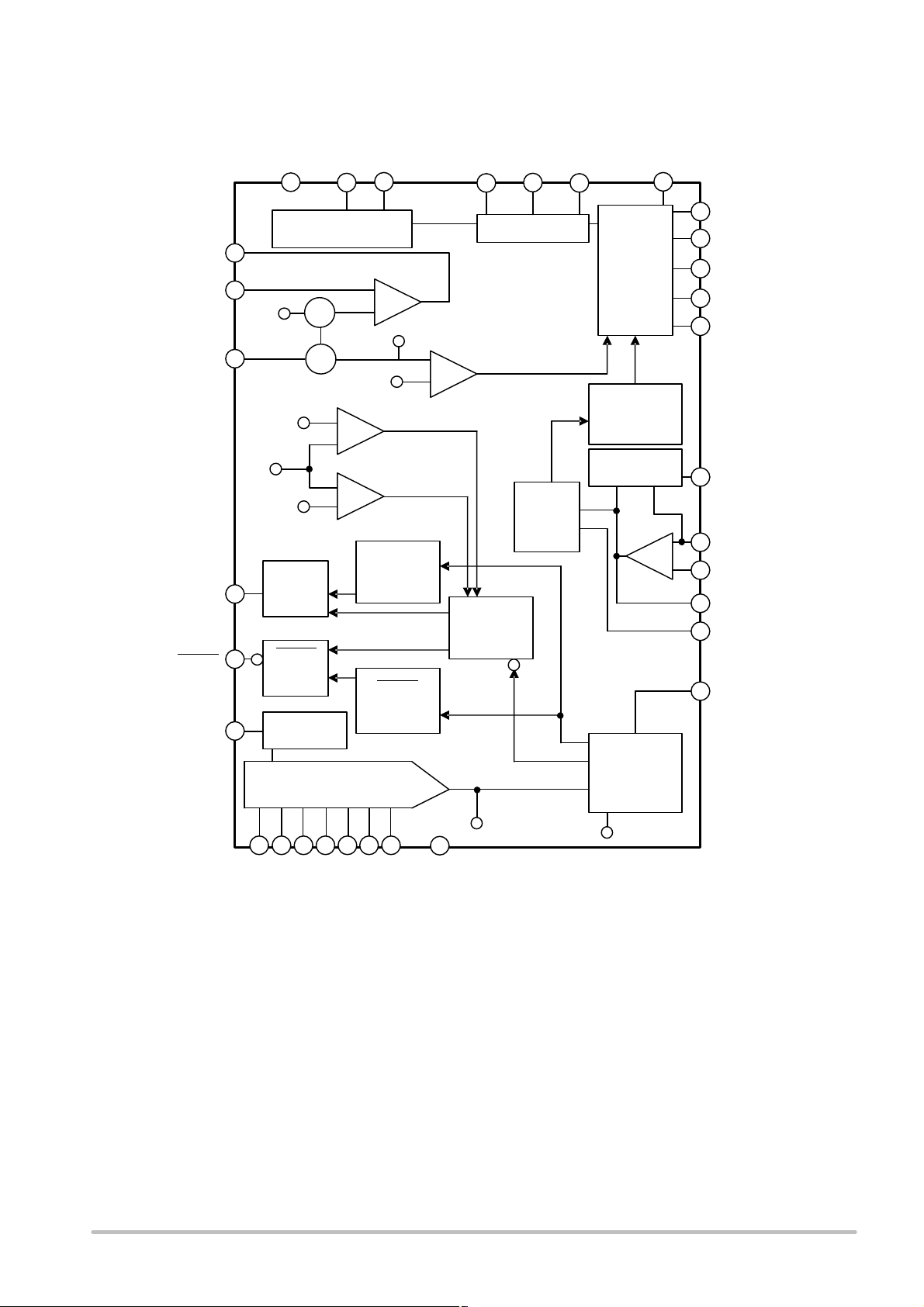
VID
DAC
VID6
VID5
VID4
VID3
VID2
VID1
VID0
Precision
Reference
FBRTN
Start Up
Delay
Open
Drain
PWRGD
PWRGD
Open
Drain
+
−
+
−
CSREF
DAC + 200mV
DAC − 300 mV
DAC
−
+
CSREF
CSFB
CSCOMP
ILIM
+
−
OVP
CSREF
1.55V
+
−
_
+
LLINE
REF
REF
+
+
VEA
FB
COMP
UVLO Shutdown
and Bias
VCCGND
Oscillator
RPM RT
MOSFET
Driver
IMON
Current
Monitor
IREF
PGND
DRVL
GPU
Soft Start
and Soft
Transient
Control
OCP
Shutdown
Delay
PVCC
Delay
Disable
Soft
Transient
Delay
Current
Limit
Circuit
PWRGD
Startup
Delay
Figure 1. Functional Block Diagram
EN
CLKEN
CLKEN
CLKEN
RAMP
BST
DRVH
SW
S
S

ADP3211, ADP3211A
http://onsemi.com
3
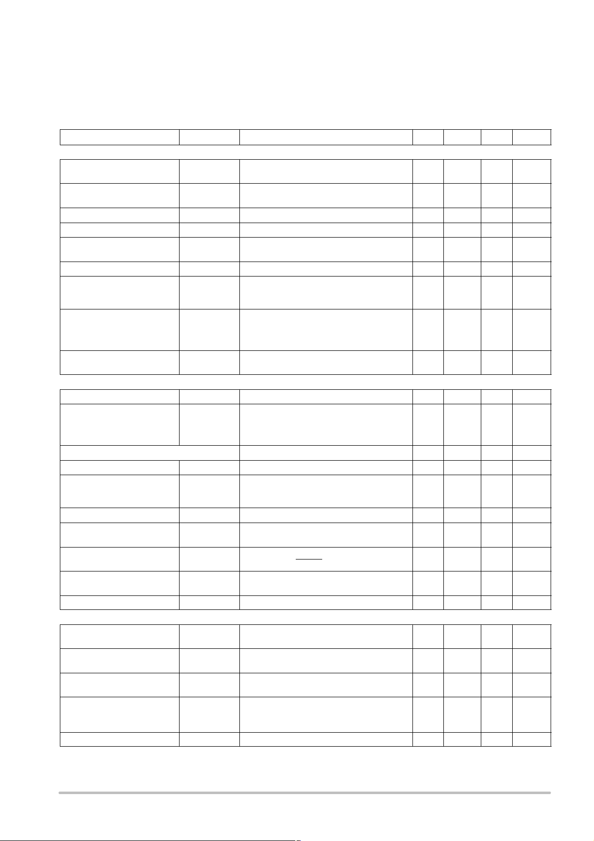
ABSOLUTE MAXIMUM RATINGS
Parameter Rating Unit
V
CC
−0.3 to +6.0 V
FBRTN, PGND −0.3 to +0.3 V
BST, DRVH
DC
t < 200 ns
−0.3 to +28
−0.3 to +33
V
BST to PV
CC
DC
t < 200 ns
−0.3 to +22
−0.3 to +28
V
BST to SW −0.3 to +6.0 V
SW
DC
t < 200 ns
−1.0 to +22
−6.0 to +28
V
DRVH to SW −0.3 to +6.0 V
DRVL to PGND
DC
t < 200 ns
−0.3 to +6.0
−5.0 to +6.0
V
RAMP (in Shutdown)
DC
t < 200 ns
−0.3 to +22
−0.3 to +26
V
All Other Inputs and Outputs −0.3 to +6.0 V
Storage Temperature Range −65 to +150 °C
Operating Ambient Temperature Range −10 to 100 °C
Operating Junction Temperature 125 °C
Thermal Impedance (qJA) 2−Layer Board 32.6 °C/W
Lead Temperature
Soldering (10 sec)
Infrared (15 sec)
300
260
°C
Stresses exceeding Maximum Ratings may damage the device. Maximum Ratings are stress ratings only. Functional operation above the
Recommended Operating Conditions is not implied. Extended exposure to stresses above the Recommended Operating Conditions may affect
device reliability.
NOTE: This device is ESD sensitive. Use standard ESD precautions when handling.

ADP3211, ADP3211A
http://onsemi.com
4
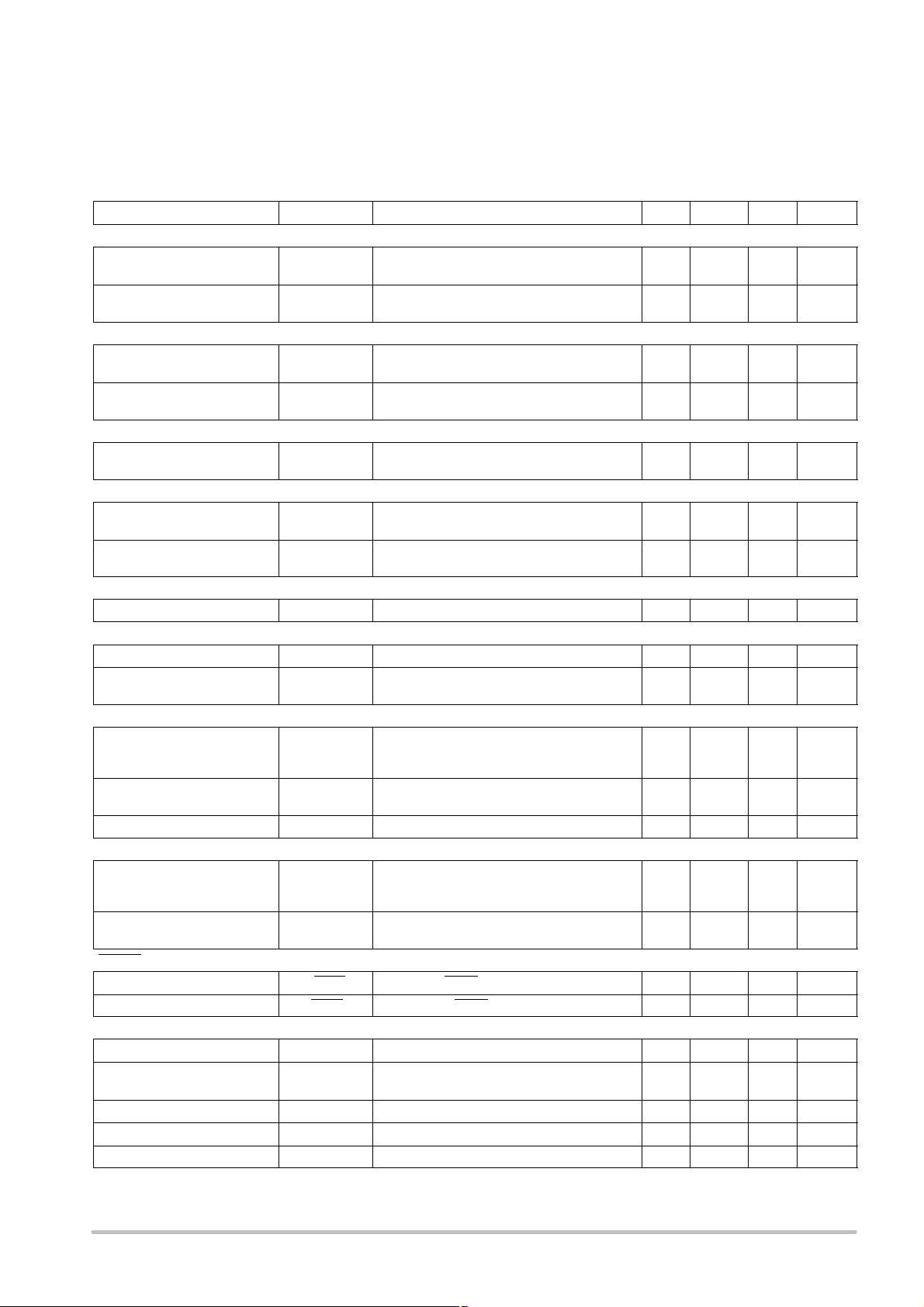
PIN FUNCTION DESCRIPTIONS
Pin No. Mnemonic Description
1 PWRGD Power−Good Output. Open−drain output. A low logic state means that the output voltage is outside of the
VID DAC defined range.
2 IMON Current Monitor Output. This pin sources current proportional to the output load current. A resistor connected
to FBRTN sets the current monitor gain.
3 CLKEN Clock Enable Output. Open drain output. The pull−high voltage on this pin cannot be higher than VCC.
4 FBRTN Feedback Return Input/Output. This pin remotely senses the GMCH voltage. It is also used as the ground
return for the VID DAC and the voltage error amplifier blocks.
5 FB Voltage Error Amplifier Feedback Input. The inverting input of the voltage error amplifier.
6 COMP Voltage Error Amplifier Output and Frequency Compensation Point.
7 GPU GMCH/CPU select pin. Connect to ground when powering the CPU. Connect to 5.0 V when powering the
GMCH. When GPU is connected to ground, the boot voltage is 1.1 V for the ADP3211 and 1.2 V for the
ADP3211A. When GPU is connected to 5.0 V, there is no boot voltage.
8 ILIM Current Limit Set pin. Connect a resistor between ILIM and CSCOMP to the current limit threshold.
9 IREF This pin sets the internal bias currents. A 80 kW is connected from IREF to ground.
10 RPM RPM Mode Timing Control Input. A resistor is connected from RPM to ground sets the RPM mode turn−on
threshold voltage.
11 RT PWM Oscillator Frequency Setting Input. An external resistor from this pin to GND sets the PWM oscillator
frequency.
12 RAMP PWM Ramp Slope Setting Input. An external resistor from the converter input voltage node to this pin sets
the slope of the internal PWM stabilizing ramp.
13 LLINE Load Line Programming Input. The center point of a resistor divider connected between CSREF and
CSCOMP tied to this pin sets the load line slope.
14 CSREF Current Sense Reference Input. This pin must be connected to the opposite side of the output inductor.
15 CSFB Non−inverting Input of the Current Sense Amplifier. The combination of a resistor from the switch node to this
pin and the feedback network from this pin to the CSCOMP pin sets the gain of the current sense amplifier.
16 CSCOMP Current Sense Amplifier Output and Frequency Compensation Point.
17 GND Analog and Digital Signal Ground.
18 PGND Low−Side Driver Power Ground. This pin should be connected close to the source of the lower MOSFET(s).
19 DRVL Low−Side Gate Drive Output.
20 PVCC Power Supply Input/Output of Low−Side Gate Driver.
21 SW Current Return For High−Side Gate Drive.
22 DRVH High−Side Gate Drive Output.
23 BST High−Side Bootstrap Supply. A capacitor from this pin to SW holds the bootstrapped voltage while the
high−side MOSFET is on.
24 VCC Power Supply Input/Output of the Controller.
25 to 31 VID6 to VID0 Voltage Identification DAC Inputs. A 7−bit word (the VID Code) programs the DAC output voltage, the
reference voltage of the voltage error amplifier without a load (see the VID Code Table, Table NO TAG). In
normal operation mode, the VID DAC output programs the output voltage to a value within the 0 V to 1.5 V
range. The input is actively pulled down.
32 EN Enable Input. Driving this pin low shuts down the chip, disables the driver outputs, and pulls PWRGD low.
ADP3211, ADP3211A
http://onsemi.com
5
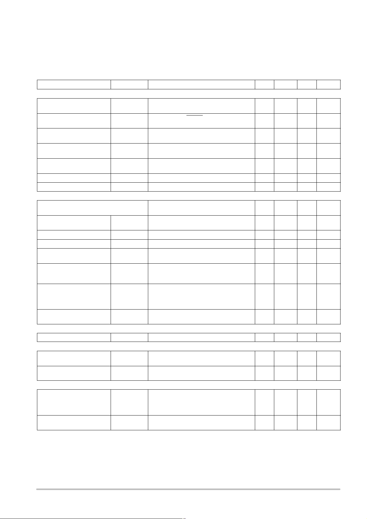
ELECTRICAL CHARACTERISTICS (V
CC
= PVCC = 5.0 V, FBRTN = GND = PGND = 0 V, H = 5.0 V, L = 0 V, V
VID
= V
DAC
= 1.2 V,
TA = −10°C to 100°C, unless otherwise noted. (Note 1) Current entering a pin (sunk by the device) has a positive sign.
Parameter Symbol Conditions Min Typ Max Units
VOLTAGE CONTROL − Voltage Error Amplifier (VEAMP)
FB, LLINE Voltage Range
(Note 2)
VFB, V
LLINE
Relative to CSREF = V
DAC
−200 +200 mV
FB, LLINE Offset Voltage
(Note 2)
V
OSVEA
Relative to CSREF = V
DAC
−0.5 +0.5 mV
FB Bias Current I
FB
−1.0 +1.0 mA
LLINE Bias Current I
LL
−50 +50 nA
LLINE Positioning Accuracy VFB − V
DAC
Measured on FB relative to nominal V
DAC
LLINE forced 80 mV below CSREF
−78 −80 −82 mV
COMP Voltage Range V
COMP
Voltage range of interest 0.85 4.0 V
COMP Current I
COMP
COMP = 2.0 V, CSREF = V
DAC
FB forced 200 mV below CSREF
FB forced 200 mV above CSREF
−650
2.0
mA
mA
COMP Slew Rate SR
COMP
C
COMP
= 10 pF, CSREF = V
DAC
,
Open loop configuration
FB forced 200 mV below CSREF
FB forced 200 mV above CSREF
10
−10
V/ms
Gain Bandwidth (Note 2) GBW Non−inverting unit gain configuration,
RFB = 1 kW
20 MHz
VID DAC VOLTAGE REFERENCE
V
DAC
Voltage Range (Note 2) See VID Code Table 0 1.5 V
V
DAC
Accuracy VFB − V
DAC
Measured on FB (includes offset), relative to
nominal V
DAC
V
DAC
= 0.3000 V to 1.2000 V
V
DAC
= 1.2125 V to 1.5000 V
−7.0
−9.0
+7.0
+9.0
mV
V
DAC
Differential Non−linearity (Note 2) −1.0 +1.0 LSB
V
DAC
Line Regulation ΔV
FB
VCC = 4.75 V to 5.25 V 0.05 %
V
DAC
Boot Voltage V
BOOTFB
Measured during boot delay period, GPU = 0 V
ADP3211
ADP3211A
1.100
1.200
V
Soft−Start Delay (Note 2) t
DSS
Measured from EN pos edge to FB = 50 mV 200 ms
Soft−Start Time t
SS
Measured from EN pos edge to FB settles to
V
boot
= 1.1 V within −5%
1.4 ms
Boot Delay t
BOOT
Measured from FB settling to Vboot = 1.1 V
within −5% to CLKEN neg edge
100 ms
V
DAC
Slew Rate Soft−Start
Arbitrary VID step
0.0625
1.0
LSB/ms
FBRTN Current I
FBRTN
70 200 mA
VOLTAGE MONITORING and PROTECTION − Power Good
CSREF Undervoltage
Threshold
V
UVCSREF
−
V
DAC
Relative to nominal V
DAC
Voltage −360 −300 −240 mV
CSREF Overvoltage
Threshold
V
OVCSREF
−
V
DAC
Relative to nominal V
DAC
Voltage 150 200 250 mV
CSREF Crowbar Voltage
Threshold
V
CBCSREF
Relative to FBRTN 1.5 1.55 1.6 V
CSREF Reverse Voltage
Threshold
V
RVCSREF
Relative to FBRTN, Latchoff Mode
CSREF is falling
CSREF is rising
−350 −300
−75 −5.0
mV
PWRGD Low Voltage V
PWRGD
I
PWRGD(SINK)
= 4 mA 75 200 mV
1. All limits at temperature extremes are guaranteed via correlation using standard statistical quality control (SQC).
2. Guaranteed by design or bench characterization, not production tested.
ADP3211, ADP3211A
http://onsemi.com
6
ELECTRICAL CHARACTERISTICS (V
CC
= PVCC = 5.0 V, FBRTN = GND = PGND = 0 V, H = 5.0 V, L = 0 V, V
VID
= V
DAC
= 1.2 V,
TA = −10°C to 100°C, unless otherwise noted. (Note 1) Current entering a pin (sunk by the device) has a positive sign.
Parameter UnitsMaxTypMinConditionsSymbol
VOLTAGE MONITORING and PROTECTION − Power Good
PWRGD High Leakage
Current
I
PWRGD
V
PWRDG
= 5.0 V 1.0 mA
PWRGD Startup Delay T
SSPWRGD
Measured from CLKEN neg edge to PWRGD
pos edge
8.0 ms
PWRGD Latchoff Delay T
LOFFPWRGD
Measured from Out−off−Good−Window event
to Latchoff (switching stops)
8.0 ms
PWRGD Propagation Delay
(Note 2)
T
PDPWRGD
Measured from Out−off−Good−Window event
to PWRGD neg edge
200 ns
Crowbar Latchoff Delay
(Note 2)
T
LOFFCB
Measured from Crowbar event to Latchoff
(switching stops)
200 ns
PWRGD Masking Time T
MSkPWRGD
Triggered by any VID change 100 ms
CSREF Soft−Stop Resistance EN = L or Latchoff condition 60 W
CURRENT CONTROL − Current Sense Amplifier (CSAMP)
CSFB, CSREF Common−Mode Range
(Note 2)
Voltage range of interest 0 2.0 V
CSFB, CSREF Offset Voltage V
OSCSA
CSREF – CSSUM, TA = 0°C to 85°C
TA = 25°C
−1.4
−0.4
+1.4
+0.4
V
CSFB Bias Current I
BCSFB
−50 +50 nA
CSREF Bias Current I
BCSREF
−2.0 2.0 mA
CSCOMP Voltage Range
(Note 2)
Voltage range of interest 0.05 2.0 V
CSCOMP Current
I
CSCOMPsource
I
CSCOMPsink
CSCOMP = 2.0 V
CSFB forced 200 mV below CSREF
CSFB forced 200 mV above CSREF
−650
1.0
mA
mA
CSCOMP Slew Rate (Note 2) C
CSCOMP
= 10 pF, CSREF = V
DAC
,
Open loop configuration
CSFB forced 200 mV below CSREF
CSFB forced 200 mV above CSREF
10
−10
V/ms
Gain Bandwidth (Note 2) GBW
CSA
Non−inverting unit gain configuration
RFB = 1 kW
20 MHz
CURRENT MONITORING AND PROTECTION − Current Reference
I
REF
Voltage V
REF
R
REF
= 80 kW to set I
REF
= 20 mA 1.55 1.6 1.65 V
CURRENT LIMITER (OCP)
Current Limit (OCP)
Threshold
V
LIMTH
Measured from CSCOMP to CSREF
R
LIM
= 4.5 kW
−130 −100 −70 mV
Current Limit Latchoff Delay Measured from OCP event to PWRGD
de−assertion
8.0 ms
CURRENT MONITOR
Current Gain Accuracy I
MON/ILIM
Measured from I
LIM
to I
MON
I
LIM
= −20 mA
I
LIM
= −10 mA
I
LIM
= −5 mA
9.5
9.4
9.0
10
10
10
10.6
10.8
11
I
MON
Clamp Voltage V
MAXMON
Relative to FBRTN, I
LIM
= −30 mA
R
IMON
= 8 kW
1.0 1.15 V
1. All limits at temperature extremes are guaranteed via correlation using standard statistical quality control (SQC).
2. Guaranteed by design or bench characterization, not production tested.
ADP3211, ADP3211A
http://onsemi.com
7
ELECTRICAL CHARACTERISTICS (V
CC
= PVCC = 5.0 V, FBRTN = GND = PGND = 0 V, H = 5.0 V, L = 0 V, V
VID
= V
DAC
= 1.2 V,
TA = −10°C to 100°C, unless otherwise noted. (Note 1) Current entering a pin (sunk by the device) has a positive sign.
Parameter UnitsMaxTypMinConditionsSymbol
PULSE WIDTH MODULATOR − Clock Oscillator
RT Voltage V
RT
RT = 243 kW, V
VID
= 1.2 V
See also VRT(V
VID
) formula
1.08 1.2 1.35 V
PWM Clock Frequency
Range (Note 2)
f
CLK
Operation of interest 0.3 3.0 MHz
RAMP GENERATOR
RAMP Voltage V
RAMP
EN = H, I
RAMP
= 60 mA
EN = L
0.9 1.0
V
IN
1.1 V
RAMP Current Range (Note 2) I
RAMP
EN = H
EN = L, RAMP = 19 V
1.0
−0.5
100
+0.5
mA
PWM COMPARATOR
PWM Comparator Offset
(Note 2)
V
OSRPM
−3.0 +3.0 mV
RPM COMPARATOR
RPM Current I
RPM
V
VID
= 1.2 V, RT = 243 kW
See also I
RPM(RT
) formula
−6.0 mA
RPM Comparator Offset
(Note 2)
V
OSRPM
V
COMP
− (1 + V
RPM
) −3.0 +3.0 mV
SWITCH AMPLIFIER
SW Input Resistance R
SW
Measured from SW to PGND 1.3 kW
ZERO CURRENT SWITCHING COMPARATOR
SW ZCS Threshold V
ZCSSW
DCM mode, DPRSLP = 3.3 V −4.0 mV
Masked Off−Time t
OFFMSKD
Measured from DRVH neg edge to DRVH
pos edge at max frequency of operation
700 ns
SYSTEM I/O BUFFERS − EN and VID[6:0] INPUTS
Input Voltage V
EN,VID[6:0]
Refers to driving signal level
Logic low, I
sink
= 1 mA
Logic high, I
source
= −5 mA 1.0
0.3
V
Input Current I
EN,VID[6:0]
V
EN,VID[6:0]
= 0 V
0.2 V < V
EN,VID[6:0]
≤ V
CC
10
1.0
nA
mA
VID Delay Time (Note 2) Any VID edge to 10% of FB change 200 ns
GPU INPUT
Input Voltage V
GPU
Refers to driving signal level
Logic low, I
sink
= 1 mA
Logic high, I
source
= −5 mA 4.0
0.3
V
Input Current I
GPU
GPU = L or GPU = H (static)
0.8 V < EN < 1.6 V (during transition)
10
70
nA
mA
CLKEN OUTPUT
Output Low Voltage V
CLKEN
Logic low, I
CLKEN
= 4 mA 30 300 mV
Output High, Leakage Current I
CLKEN
Logic high, V
CLKEN
= V
CC
3.0 mA
SUPPLY
Supply Voltage Range V
CC
4.5 5.5 V
Supply Current EN = H
EN = L
6.0
60
10
200
mA
mA
VCC OK Threshold V
CCOK
VCC is rising 4.4 4.5 V
VCC UVLO Threshold V
CCUVLO
VCC is falling 4.0 4.15 V
VCC Hysteresis (Note 2) 150 mV
1. All limits at temperature extremes are guaranteed via correlation using standard statistical quality control (SQC).
2. Guaranteed by design or bench characterization, not production tested.
ADP3211, ADP3211A
http://onsemi.com
8
ELECTRICAL CHARACTERISTICS (V
CC
= PVCC = 5.0 V, FBRTN = GND = PGND = 0 V, H = 5.0 V, L = 0 V, V
VID
= V
DAC
= 1.2 V,
TA = −10°C to 100°C, unless otherwise noted. (Note 1) Current entering a pin (sunk by the device) has a positive sign.
Parameter UnitsMaxTypMinConditionsSymbol
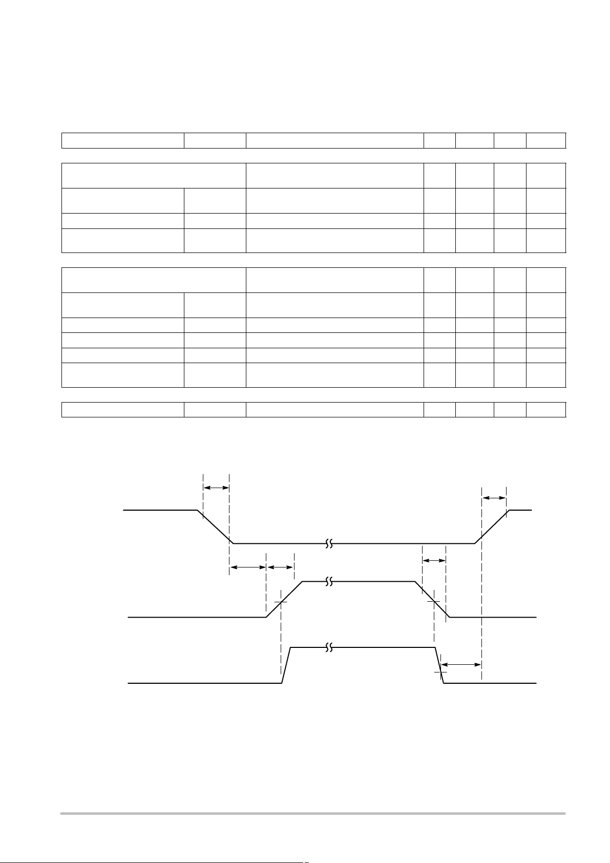
HIGH−SIDE MOSFET DRIVER
Pullup Resistance, Sourcing Current
Pulldown Resistance, Sinking Current
BST = PV
CC
2.0
1.0
3.3
2.8
W
Transition Times tr
DRVH,
tf
DRVH
BST = PVCC, CL = 3 nF, Figure 2 15
13
35
31
ns
Dead Delay Times tpdh
DRVH
BST = PVCC, Figure 2 10 45 ns
BST Quiescent Current EN = L (Shutdown)
EN = H, No Switching
5.0
200
15 mA
LOW−SIDE MOSFET DRIVER
Pullup Resistance, Sourcing Current
Pulldown Resistance, Sinking Current
1.8
0.9
3.0
2.7
W
Transition Times tr
DRVL,
tf
DRVL
CL = 3 nF, Figure 2 15
14
35
35
ns
Propagation Delay Times tpdh
DRVL
CL = 3 nF, Figure 2 15 30 ns
SW Transition Timeout t
SWTO
DRVH = L, SW = 2.5 V 150 250 450 ns
SW Off Threshold V
OFFSW
2.2 V
PVCC Quiescent Current EN = L (Shutdown)
EN = H, No Switching
14
200
50 mA
BOOTSTRAP RECTIFIER SWITCH
On−Resistance EN = L or EN = H and DRVL = H 4 7 11 W
1. All limits at temperature extremes are guaranteed via correlation using standard statistical quality control (SQC).
2. Guaranteed by design or bench characterization, not production tested.
3. Timing is referenced to the 90% and 10% points, unless otherwise noted.
DRVH
(with respect to SW)
DRVL
SW
1.0 V
Figure 2. Timing Diagram
V
TH
V
TH
tf
DRVL
tpdh
DRVH
tr
DRVH
tf
DRVH
tr
DRVL
tpdh
DRVL

ADP3211, ADP3211A
http://onsemi.com
9
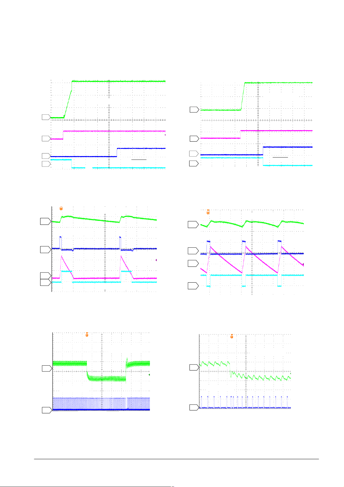
TYPICAL PERFORMANCE CHARACTERISTICS
V
VID
= 1.5 V, TA = 20°C to 100°C, unless otherwise noted.
1
2
3
1: 200mV/div
2: 2V/div
3
: 10V/div
Input = 12V, 1A Load
VID Step 0.7V to 1.2V
Figure 3. VID Change Soft Transient
1
2
3
1: 200mV/div
2: 2V/div
3: 10V/div
Input = 12V, 1A Load
VID Step 1.2V to 0.7V
Figure 4. VID Change Soft Transient
20 ms/div
Output Voltage
VID5
Switch Node
20 ms/div
VID5
Switch
Node
Output Voltage
Figure 5. Switching Frequency vs. Load
Current in RPM Mode
Figure 6. I
MON
Voltage vs. Load Current
LOAD CURRENT (A) LOAD CURRENT (A)
151050
0
50
100
150
200
250
300
2520151050
0
0.2
0.4
0.6
0.8
1.0
1.2
Figure 7. Load Line Accuracy Figure 8. VCC Current vs. VCC Voltage with
Enable Low
LOAD CURRENT (A) VCC VOLTAGE (V)
151050
1.15
1.20
1.25
1.30
1.35
6543210
0
10
20
30
50
60
70
80
SWITCHING FREQUENCY (kHz)
I
MON
(V)
VID VOLTAGE (V)
V
CC
CURRENT (mA)
OUTPUT RIPPLE
SWITCHING
FREQUENCY
OUTPUT RIPPLE (mV)
30
35
40
45
50
55
60
+2%
−2%
Specified Load Line
Measured Load Line
40
ADP3211, ADP3211A
http://onsemi.com
10
TYPICAL PERFORMANCE CHARACTERISTICS
EN
1
2
3
4
1: 0.5V/div
2: 5V/div
3: 5V/div
4: 5V/div
2ms/div
GPU = 0V
Figure 9. Startup Waveforms CPU Mode
EN
1
2
3
4
1: 0.5V/div
2: 5V/div
3: 5V/div
4: 5V/div
4ms/div
GPU = 5V
Figure 10. Startup Waveforms GPU Mode
1
2
3
4
1 : 100mV/div
2 : 10V/div
3: 5A/div
4 : 5V/div
Low Side Gate Drive
Figure 11. DCM Waveforms, 1 A Load Current
1
2
3
4
1 : 100mV/div
2 : 10V/div
3 : 5A/div
4 : 5V/div
Figure 12. CCM Waveforms, 10 A Load Current
1
2
1: 50mV/div
2: 10V/div
Output Voltage
Switch Node
Input = 12V
Output = 1.2V
3A to 15A Step
Figure 13. Load Transient Figure 14. Load Transient
1
2
1: 50mV/div
2: 10V/div
Output Voltage
Switch Node
Input = 12V
Output = 1.2V
3A to 15A Step
Output Voltage
CLKEN
PWRGD
40 ms/div
40 ms/div
2 ms/div
Low Side Gate Drive
Output Voltage
Inductor
Current
Switch Node
4 ms/div
Inductor
Current
Output Voltage
Switch Node
PWRGD
Output Voltage
CLKEN
 Loading...