

ON Semiconductor 2N4921, 2N4922, 2N4923 Service Manual
2N4921, 2N4922, 2N4923
Î
Î
Î
Î
Î
Î
Î
Î
Î
Î
Î
Î
Î
Î
Î
Î
2N4923 is a Preferred Device
Medium−Power Plastic
NPN Silicon Transistors
These high−performance plastic devices are designed for driver
circuits, switching, and amplifier applications.
Features
• Low Saturation Voltage − V
= 0.6 Vdc (Max) @ IC = 1.0 A
CE(sat)
• Excellent Power Dissipation Due to Thermopad Construction −
PD = 30 W @ TC = 25_C
• Excellent Safe Operating Area
• Gain Specified to I
= 1.0 A
C
• Complement to PNP 2N4918, 2N4919, 2N4920
• Pb−Free Packages are Available*
MAXIMUM RATINGS
Rating Symbol Value Unit
Collector−Emitter Voltage 2N4921
ОООООООООО
2N4922
2N4923
Collector−Emitter Voltage 2N4921
ОООООООООО
2N4922
2N4923
Emitter Base Voltage
Collector Current − Continuous (Note 1)
ОООООООООО
Base Current − Continuous
Total Power Dissipation @ TC = 25_C
Derate above 25_C
Operating and Storage Junction
ОООООООООО
Temperature Range
THERMAL CHARACTERISTICS (Note 2)
Characteristic Symbol Max Unit
Thermal Resistance, Junction−to−Case
Maximum ratings are those values beyond which device damage can occur.
Maximum ratings applied to the device are individual stress limit values (not
normal operating conditions) and are not valid simultaneously. If these limits are
exceeded, device functional operation is not implied, damage may occur and
reliability may be affected.
1. The 1.0 A maximum IC value i s b ased u pon J EDEC c urrent g ain r equirements.
The 3.0 A maximum value is based upon actual current handling capability of
the device (see Figures 5 and 6).
2. Recommend use of thermal compound for lowest thermal resistance.
*Indicates JEDEC Registered Data.
*For additional information on our Pb−Free strategy and soldering details, please
download the ON Semiconductor Soldering and Mounting Techniques
Reference Manual, SOLDERRM/D.
V
CEO
Î
V
Î
V
I
Î
I
P
TJ, T
Î
q
CB
EB
C
B
D
stg
JC
40
60
ÎÎ
80
40
ÎÎ
60
80
5.0
1.0
ÎÎ
3.0
1.0
30
0.24
– 65 to +150
ÎÎ
4.16
Vdc
ÎÎ
Vdc
ÎÎ
Vdc
Adc
ÎÎ
Adc
W
mW/_C
_C
ÎÎ
_C/W
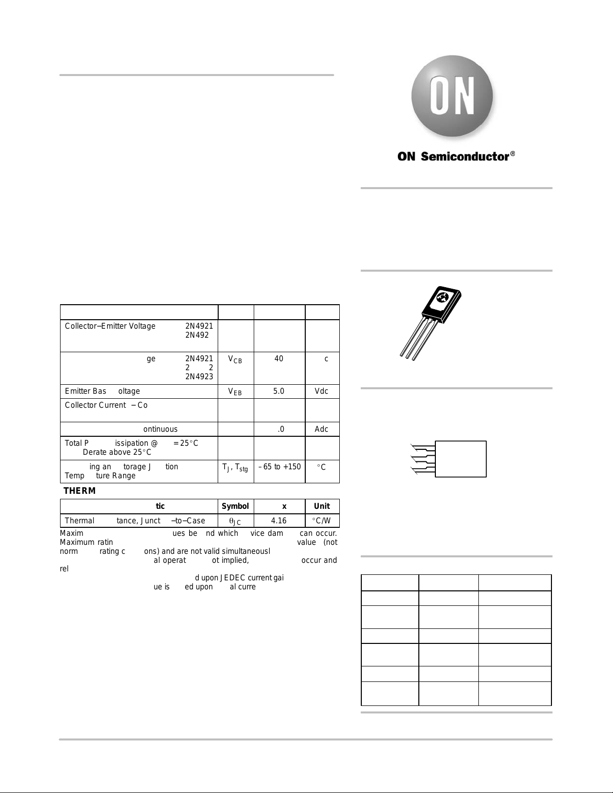
http://onsemi.com
1.0 AMPERE
GENERAL PURPOSE
POWER TRANSISTORS
40−80 VOLTS, 30 WATTS
TO−225
CASE 77
3
2
1
MARKING DIAGRAM
1
Y = Year
WW = Work Week
2N492x = Device Code
G = Pb−Free Package
ORDERING INFORMATION
Device Package Shipping
2N4921 TO−225 500 Units / Box
2N4921G TO−225
2N4922 TO−225 500 Units / Box
2N4922G TO−225
2N4923 TO−225 500 Units / Box
2N4923G TO−225
Preferred devices are recommended choices for future use
and best overall value.
(Pb−Free)
(Pb−Free)
(Pb−Free)
STYLE 1
YWW
2
N492xG
x = 1, 2, or 3
500 Units / Box
500 Units / Box
500 Units / Box
© Semiconductor Components Industries, LLC, 2006
January, 2006 − Rev. 11
1 Publication Order Number:
2N4921/D
2N4921, 2N4922, 2N4923
Î
Î
Î
Î
Î
Î
Î
Î
Î
Î
Î
Î
Î
Î
Î
Î
Î
Î
Î
Î
Î
Î
Î
Î
Î
Î
Î
Î
Î
Î
Î
Î
Î
Î
Î
Î
Î
Î
Î
Î
Î
Î
Î
Î
Î
Î
Î
Î
Î
Î
Î
Î
Î
Î
Î
Î
Î
Î
Î
Î
Î
Î
Î
Î
Î
ELECTRICAL CHARACTERISTICS (T
= 25_C unless otherwise noted)
C
Characteristic
OFF CHARACTERISTICS
Collector−Emitter Sustaining Voltage (Note 3)
(IC = 0.1 Adc, IB = 0) 2N4921
ООООООООООООООООООО
ООООООООООООООООООО
2N4922
2N4923
Collector Cutoff Current
(VCE = 20 Vdc, IB = 0) 2N4921
(VCE = 30 Vdc, IB = 0) 2N4922
ООООООООООООООООООО
(VCE = 40 Vdc, IB = 0) 2N4923
ООООООООООООООООООО
Collector Cutoff Current
ООООООООООООООООООО
(VCE = Rated V
(VCE = Rated V
ООООООООООООООООООО
CEO
CEO
, V
, V
= 1.5 Vdc)
EB(off)
= 1.5 Vdc, TC = 125_C
EB(off)
Collector Cutoff Current
(VCB = Rated VCB, IE = 0)
Emitter Cutoff Current
ООООООООООООООООООО
(VEB = 5.0 Vdc, IC = 0)
ON CHARACTERISTICS
DC Current Gain (Note 3)
(IC = 50 mAdc, VCE = 1.0 Vdc)
ООООООООООООООООООО
(IC = 500 mAdc, VCE = 1.0 Vdc)
(IC = 1.0 Adc, VCE = 1.0 Vdc)
ООООООООООООООООООО
Collector−Emitter Saturation Voltage (Note 3)
(IC = 1.0 Adc, IB = 0.1 Adc)
Base−Emitter Saturation Voltage (Note 3)
ООООООООООООООООООО
(IC = 1.0 Adc, IB = 0.1 Adc)
Base−Emitter On Voltage (Note 3)
(IC = 1.0 Adc, VCE = 1.0 Vdc)
ООООООООООООООООООО
SMALL−SIGNAL CHARACTERISTICS
Current−Gain − Bandwidth Product
(IC = 250 mAdc, VCE = 10 Vdc, f = 1.0 MHz)
Output Capacitance
(VCB = 10 Vdc, IE = 0, f = 100 kHz)
ООООООООООООООООООО
Small−Signal Current Gain
(IC = 250 mAdc, VCE = 10 Vdc, f = 1.0 kHz)
ООООООООООООООООООО
3. Pulse Test: PW ≈ 300 ms, Duty Cycle ≈ 2.0%.
*Indicates JEDEC Registered Data.
Symbol
V
CEO(sus)
ÎÎÎ
ÎÎÎ
I
CEO
ÎÎÎ
ÎÎÎ
I
CEX
ÎÎÎ
ÎÎÎ
I
CBO
I
EBO
ÎÎÎ
h
FE
ÎÎÎ
ÎÎÎ
V
CE(sat)
V
BE(sat)
ÎÎÎ
V
BE(on)
ÎÎÎ
f
T
C
ob
ÎÎÎ
h
fe
ÎÎÎ
Min
40
ÎÎ
60
80
ÎÎ
−
ÎÎ
−
−
ÎÎ
ÎÎ
−
−
ÎÎ
−
ÎÎ
−
40
ÎÎ
30
10
ÎÎ
−
ÎÎ
−
−
ÎÎ
3.0
−
ÎÎ
25
ÎÎ
Max
−
Î
−
−
Î
0.5
Î
0.5
0.5
Î
Î
0.1
0.5
Î
0.1
Î
1.0
−
Î
150
−
Î
0.6
Î
1.3
1.3
Î
−
100
Î
−
Î
Unit
Vdc
ÎÎ
ÎÎ
mAdc
ÎÎ
ÎÎ
mAdc
ÎÎ
ÎÎ
mAdc
mAdc
ÎÎ
−
ÎÎ
ÎÎ
Vdc
Vdc
ÎÎ
Vdc
ÎÎ
MHz
pF
ÎÎ
−
ÎÎ
http://onsemi.com
2
 Loading...