

Page 1
SERVICE MANUAL
SERVICE MANUAL
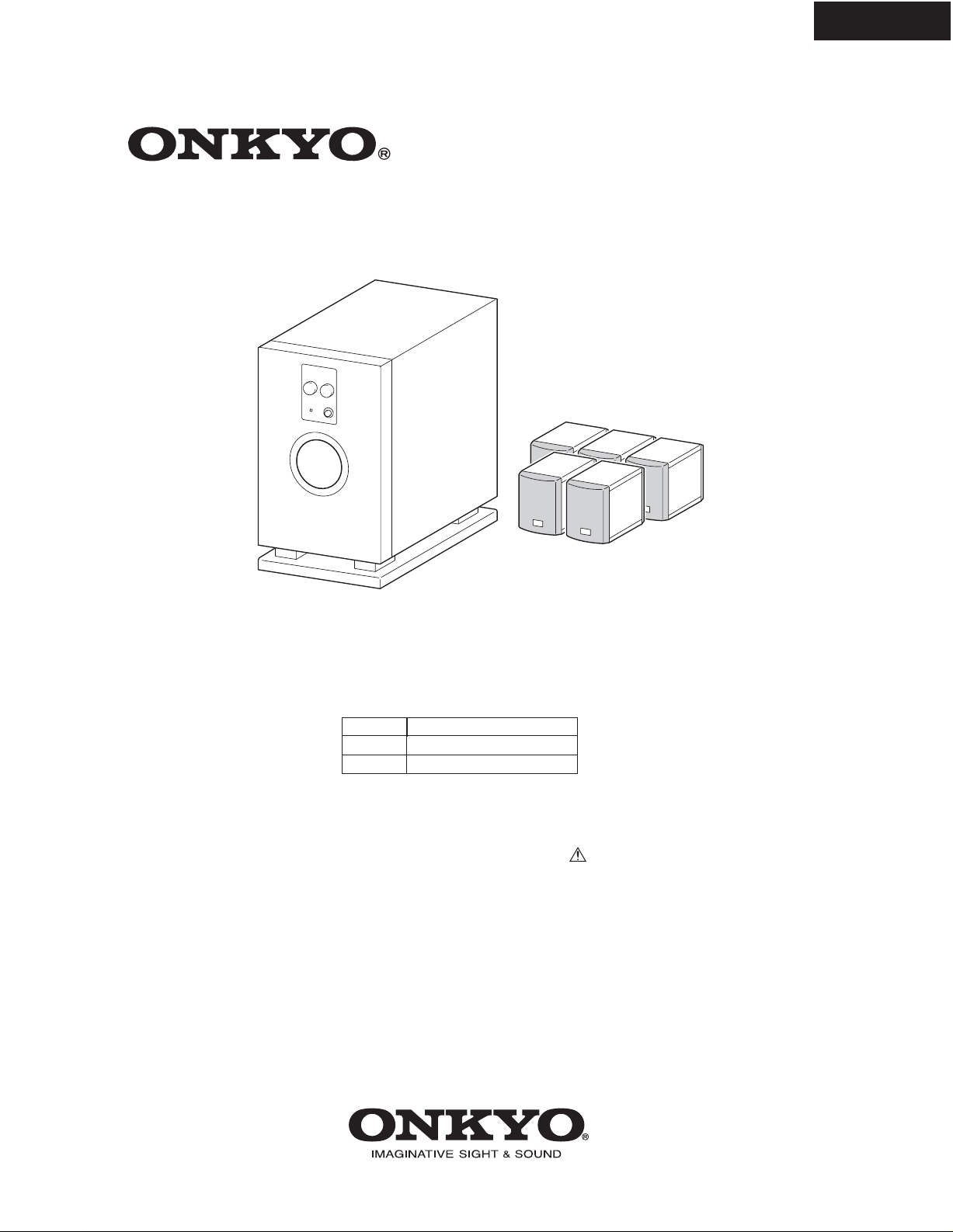
SUB WOOFER SYSTEM
SL-105 / HTP-2
SL-105
Ref. No.3709
082001
POWERED SUBWOOFER
Black color : MPP model
Yellow color : MDT, MGT models
D-L5 x 5
SATELLITE SPEAKERS
SL-105
MPP 230-240V AC, 50Hz
MDT 120V AC, 60Hz
MGT 220-230V AC, 50/60Hz
SAFETY-RELATED COMPONENT
WARNING!!
COMPONENTS IDENTIFIED BY MARK ON THE
SCHEMATIC DIAGRAM AND IN THE PARTS LIST ARE
CRITICAL FOR RISK OF FIRE AND ELECTRIC SHOCK.
REPLACE THESE COMPONENTS WITH ONKYO
PARTS WHOSE PART NUMBERS APPEAR AS SHOWN
IN THIS MANUAL.
MAKE LEAKAGE-CURRENT OR RESISTANCE
MEASUREMENTS TO DETERMINE THAT EXPOSED
PARTS ARE ACCEPTABLY INSULATED FROM THE
SUPPLY CIRCUIT BEFORE RETURNING THE
APPLIANCE TO THE CUSTOMER.
Page 2

SERVICE NOTE
1. Replacing the fuses
This symbol located near the fuses indicates that the fuse used is
fast operating type. For continued protection against fire hazard, replace with same type fuse. For fuse rating refer to the marking adjacent to the symbol.
Ce symbole indique que le fusible utlise est a rapide. Pour une protection permanente, n'untiliser que fusibles de meme type. Ce darnier est la qu le present symbol est appse.
CIRCUIT NO. PART NO. DESCRIPTION
CIRCUIT NO. PART NO. DESCRIPTION
F901,F903 252069 or 0.8A-SE-EAK or
252236 800MA-SE-TL250V <MPP,MGT>
F902 252159 or 2A-UL/T-237 or
252253 2A-T/UL-ST2 <MDT>
SL-105
2. Safety-check out
After correcting the original service problem, perform the following
safety check before releasing the set to the customer. Connect the insulating-resistance tester between the plug of power supply cord and
screw on the back panel.
Specifications: 3.3MohmrCV8
Page 3
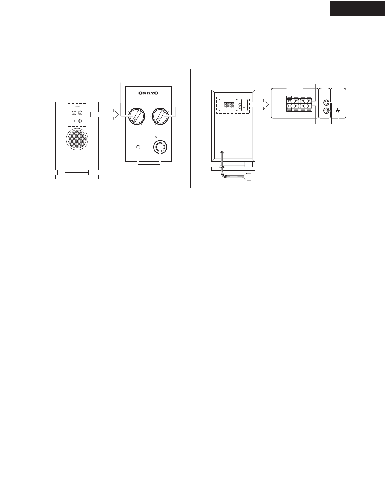
PANEL VIEW
Subwoofer SL-105
SL-105
Front panel
SL-105
23
POWERED SUBWOOFER
LEVEL
200Hz
OUTPUT
MIN MAX
POWER
FREQUENCY
50Hz
1
1 Power switch (POWER) and indicator
Pressing this button turns the power on (the indicator
lights). Pressing the button again turns the power off
(the indicator goes out).
Red: Unit is in standby mode
Green: Unit is in operation
2 Frequency adjusting knob (FREQUENCY)
Use this knob to select the high-frequency range at
which you wish to cut off the signal to the subwoofer.
You can select any frequency between 50 Hz and 200
Hz depending on the characteristics of the speaker
system being used with the SL-105.
3 Output level adjusting knob (OUTPUT LEVEL)
Use this knob to adjust the output level of the
subwoofer.
Rear panel
SL-105
INPUT
AMP/RECEIVER
OUTPUT
TO SPEAKERS
FROM
SPEAKER LEVEL
R
+
R
+
C
LINE
_
_
_
_
INPUT
L
+
L
(MONO)
R
L
+
DAB
To AC outlet
A Low-level input jacks (LINE INPUT)
Connect these jacks to the LINE OUT jacks of the
amplifier etc.
B Auto standby switch (AUTO STANDBY)
This switch is used to turn on and off the auto standby
function.
ON: This activates the auto standby function.
If a constant level signal is not received from the
amplifier (or receiver) over a period of a few minutes,
the SL-105 automatically enters the standby state. If a
constant level signal is later received from the amplifier
(or receiver), the power is automatically turned back on.
OFF: Deactivates the auto standby function.
Notes:
The auto standby function operates on the existence
*
or absence of a constant level input signal. If the auto
standby function does not operate properly, try
slightly increasing (or decreasing) the output level of
the amplifier or receiver. (Note that output levels of
some amplifiers and receivers cannot be adjusted.
For more details regarding your components, refer to
the instruction manual supplied with them.)
If noise from peripheral components causes the
*
incorrect operation of the auto standby function, or if
outputting low volumes (i.e., during the nighttime)
causes the auto standby function to activate, turn off
the auto standby function.
The auto standby function only operates while the
*
power switch for the SL-105 is turned on.
C Speaker-level input terminals
(INPUT FROM AMP/RECEIVER)
Connect these input terminals to the speaker output
terminals of your amplifier or receiver.
D Speaker-level output terminals
(OUTPUT TO SPEAKERS)
The speaker-level signal to the front speakers is output
from these terminals.
AUTO STANDBY
OFF ON
Page 4
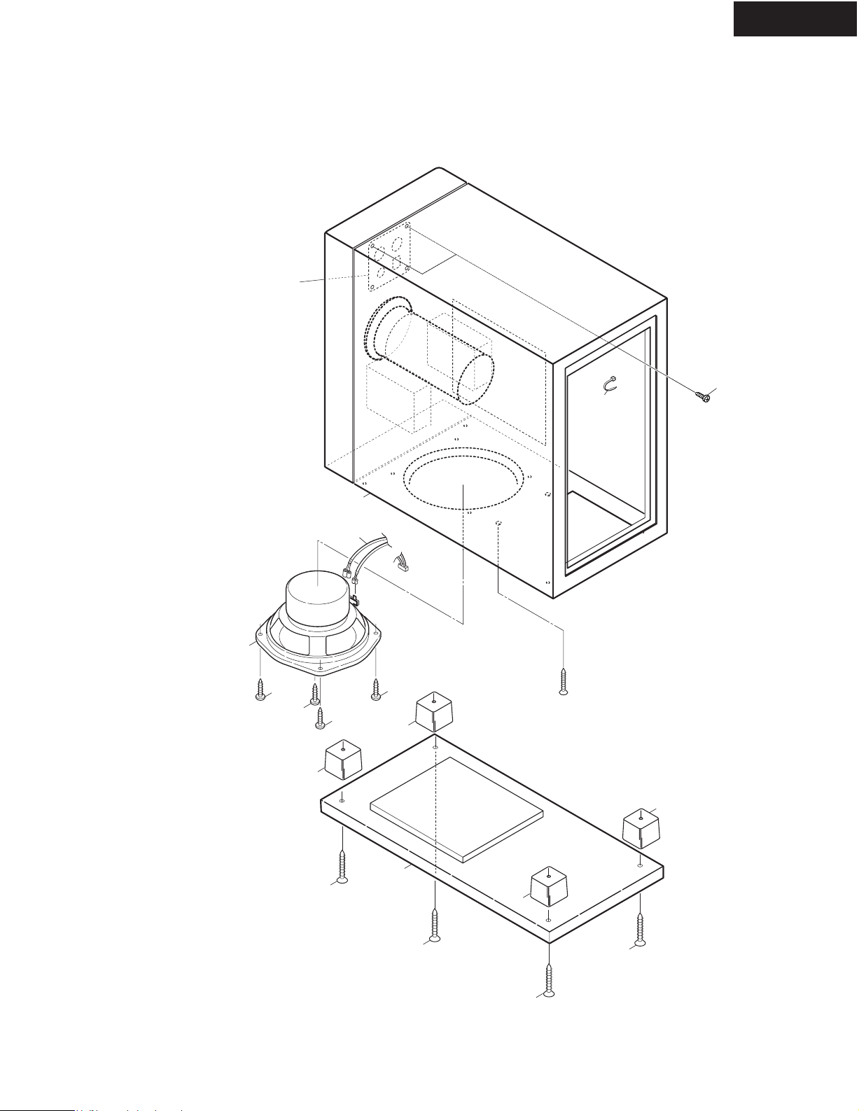
EXPLODED VIEW
(CABINET SECTION)
SL-105
Indicated in the exploded view of
an amplifier section.
S10
S3
E901
S9
S1
P535
S7
S7
S7
S4
S8
S7
S4
S4
S2
S4
S8
S8
S8
Page 5
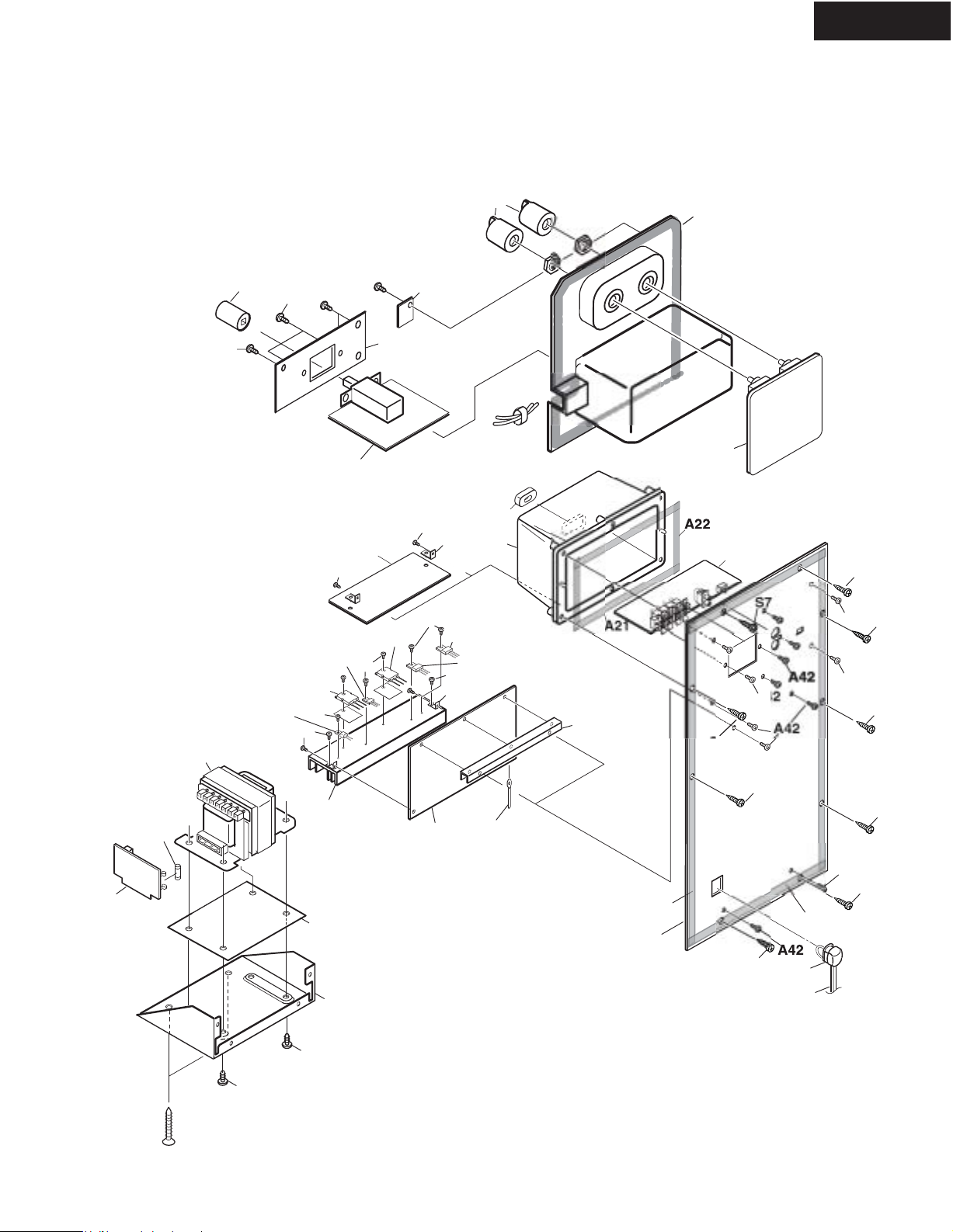
A49
8
U2
S7
S3
CHASSIS EXPLODED VIEW
(AMPLIFIER SECTION)
SL-105
S6
A18
S5
A18
R602
Q541
Q515
A2
A5
A5
U4
A2
Q515A
U3
U7
Q516
Q516B
U8
A5
A2
A4
Q951
Q952
A5
A4
A20
A15
A8
U6
S7
A42
A42
S7
S7
U5
F901
T901
A43
A52
A43
A1
A30
U1
E811
A4
A41
S7
S7
S7
A42
S7
A55
P901
Page 6
SL-105
EXPLODED VIEW PARTS LIST
<AMPLIFIER ASSEMBLY PARTS LIST>
REF. NO. PART NO. DESCRIPTION
A1 27160467 Heat sink, SKW-205AMP
A2 801433 3SMS8W.SW+14B(BC), Self tapping screw
A4
A5 838130088 3TTB+8B, Self tapping screw
A8
A15
A18 82143010 3P+10FN(BC), PAN head screw
A20 28141322A Cushion
A21 28141417 Cushion, P t1x5x160
A22 28141418 Cushion, Q t1x5x80
A30
A41 27122929 Rear panel <MPP>
A42 838430088 3TTB+8B(BC), Self tapping screw
A43 830440109 4TTC+10C(BC), Self tapping screw
A48
A49 28141416 Cushion, O t1x5x195
A52 28141334 Insulation sheet
A55 27301941 Cord bushing, KF-41
E811,E814
E901
F901 252069 0.8A-SE-EAK or
P535 2009990611UL NSAS-2P0833, Socket assy
P901 253175 AS-CEE ZA, Power cord <MPP,MGT>
Q515
Q515A,Q516A 223021 TBM-51W 9043, Isolation plate
Q516
Q541
Q951
Q952
R602
T901 2301460 NPT-1396P, Power transformer <MPP>
27130745 Bracket
27141661 Retainer
28184777 Cover
27100412 Chassis
27122930 Rear panel <MDT>
27122931 Rear panel <MGT>
28141479 Cushion, t1X5X335
27255004 Clip
260208 Wire tie
252236 800MA-SE-TL250V, Fuse <MPP.MGT>
252159 2A-UL/T-237 or
252253 2A-T/UL-ST2, Fuse <MDT>
253272HIT AS-UC-6#18, Power cord <MDT>
2203063 2SC5198-O or
*
2202523 2SC4468-O or
*
2202524 2SC4468-Y or
*
2202526 2SC4468-P or
*
2203062 2SC5198-R, Transistor
*
2203053 2SA1941-O or
*
2202513 2SA1695-O or
*
2202514 2SA1695-Y or
*
2202516 2SA1695-P or
*
2203052 2SA1941-R, Transistor
*
2202104 2SC3423-Y or
2202103 2SC3423-O, Transistor
2202754 2SD1266-P, Transistor
2202764 2SB941-P, Transistor
4000144 PTH9M04-2.2K, Thermistor
2301487 NPT-1396D, Power transformer <MDT>
2301562
NOTE: THE COMPONENTS IDENTIFIED BY MARK
ARE CRITICAL FOR RISK OF FIRE AND
ELECTRIC SHOCK. REPLACE ONLY WITH
PART NUMBER SPECIFIED.
CAUTION:
Replacement of the transistor of mark , if necessary
must be made from the same beta group (HFE) as the
original type.
NOTE:
NPT-1396G, Power transformer <MGT>
*
<MPP> European model
<MDT> Taiwanese model only
<MGT> Asian model only
<Y> Yellow color model
<B> Black color model MPP only
Page 7

BLOCK DIAGRAM
SL-105
SPEAKER
INPUT/OUTPUT
IN
RCA
C366
-19dB
BAL
+9.5dB
Q302
(1/2)
Q301
-6dB
R321
4.7K
R319
4.7K
NAAF-6866-3
Q302
(2/2)
AUTO_
STANDBY
ON/OFF
CIRCUIT
NAETC-6870-3
LEVEL
R328
NAETC-6867-3
AUTO_
STANDBY
CANCEL
NAAF-6866-3
+21dB
Q303
SW
LPF
12DB/OCT
50-200HZ
MUTE
CIRCUIT
CUTOFF FREQUENCY
VOLUME
LPF
12DB/OCT
50-200HZ
THERMAL
PROTECTION
CIRCUIT
SPEAKER
5OHHM
+28dB
POWER AMP.
NAAF-6865-3
+5.6V
1
+14.4V
1
-14.4V
1
+B
1
GND
1
-B
1
Q951
O
G
I
Q952
O
G
D931
D933
C931
I
D911
D_ARRAY
C912 C911
D932
T901
POWER
TRANS
NASW-6868-3
NAPS-6869-3
AC IN
MJJ
MDT
MPP
MGT
AC100V
AC120V
AC230V
AC220V
Page 8

M
2
-
2
C
1
R
4
)
2
4
8
8
K
T
SCHEMATIC DIAGRAM
SL-105
P301
LEVELSP
R305
12K
R306
12K
C366
223Z
AUTO
INPUT
INPUT/OUTPUT
LCH
RCH
NAAF-6865-3
47/16
R307
R309
P302
R310
R308
C305
100
100
100
100
2
3
102K
4.7K
2.2K
2.2K
4.7K
102K
S301
Q302
C315
R311
R313
R314
R312
C316
R318
18K
C306
101
M5218
102K
C318
R301
100K
R303
100K
C317
102K
R304
100K
R302
100K
1
SWCANCELPOWER
8.2K
5.6K
1K
R371
R372
R319
4.7K
R317
47/16
47/16
C301
C302
C320
47/16
-14.4
R326
100K
R316
10K
R322
22K
M5218
8
5
7
Q301
6
4
5.6K
R315
M5218
3
1
Q301
2
R320
10K
JL953B
JL953A
Q951
2SD1266
14.4 37.6
C953
220/16
C951
220/16
C952
220/16
-15.0
C954
220/16
Q952
2SB941
NAAF-6866-3
R323
22K
4
M5218
6
Q302
7
5
8
R324
0
C955
220/16
R327
100K
C956
220/16
R321
4.7K
R951
47
(1/4W)
15.0
R953
6.8K
(1/2W)
D951
MTZJ15C
D952
MTZJ15C
R954
6.8K
(1/2W)
-37.6
R952
47
(1/4W)
NAETC-6870-3
R328
(2/2)
LEVEL
P304B
470
R346
C340
0.1
JL303A
JL303B
P501
R615
12K
(1/2W)
R328
0.1
C339
C501
220/6.3
C502
151
C527
47/50
D615
1SS133
20KA
(1/2)
C322
47/16
R501
1K
R502
33K
R510
R329
22K
P304A
47K
5
6
R330
C503
151
Q303
1K
0
-37.8V
M5218
R331
10K
R505
1K
(1/4W)
Q501
2SC1775
R521
220
Q504
2SC2240
7
R336
R506
1K
(1/4W)
Q502
2SC1775
-0.6
R522
220
R503
5.6K
Q503
2SC2240
-38.4V
R504
270
R355
2.2K
Q509
R515
12K
R516
12K
Q510
(1/
R51
82
(1/4W
5
C3
1
R5
8
R
R349
47K
8
3
1
Q303
2
4
37.9V
37.9V
R509
330
R527
1K
C504
470/6.3
M5218
C505
020
R507
33K
0
R508
47
(1/4W)
R511
82
(1/4W)
Q505
2SA949-Y
Q507
2SA949-Y
2SA949-Y
2SC2229-Y
-37.9V
Q506
2SC2229-Y
R512
82
(1/4W)
0
C621
10/50
R621
5.6K
R622
100K
R623
180
C622
10/50
R610
1K
Q604
DTA124ES
P604
2SA933S
Q605
2SA933S-S
JL641A
Q603
R607
10K
5.6
5.5
2SC1740S
JL641B
5.0
R609
100K
R606
2.2M
NAE
R60
100
Q60
S
5.4
8
5
6
0
D621
Q624
4
M5218
R624
150K
D622
MTZJ2.7B
0
7
R625
10K
D627
2
3
R626
10K
Q624
R627
22
R628
22
D628
M5218
1
P623
C623
R636
39K
220/16
R629
390K
R630
820K
0
Q621
0.40.4
R632
R633
120K
R631
39K
0
DTC124ES
C630
Q622
2SC1740S-S
470K
D633
1SS133
104
5.6
Q606
2SA933S-S
R613
22K
4.9
R638
1K
R639
100K
R611
100K
5.4
R612
22K
Page 9

2
20KB
W
P305B
CROSSOVER
(1/2)
R356
(2/2)
R356
20KB
SL-105
NOTE
.
THE COMPONENTS IDENTFIED
REPLACE ONLY
.
VOLTAGE (MEASURED WITH IS
.
ELECTROLYTIC CAPACITORS (
.
ALL CAPACITORS ARE IN pF/50WV UNLESS OTHERWISE NOTED.
EX) 030 3pF 330 33pF 331 330pF
.
ALL RESISTORS ARE IN OHMS 1/4WATTS
.
THE THICK LINES ON PC BOARD ARE THE PRINTING SIDE OF THE PARTS.
EX) PRINTING SIDE
.
CIRCUIT IS SUBJECT TO CHANGE FOR IMPROVEMENT.
WITH PART
NUMBER SPECIFIED.
ARE CRITICAL FOR SAFETY.
MARKBY
DCVOLTAGE.
ARE IN F/WV.
)
333 0.033uF
(NO INPUT SIGNAL)
u
UNLESS OTHERWISE NOTED.
P305A
R355
2.2K
Q509
R515
12K
R516
12K
Q510
C343
R513
(1/4W)
R514
82
(1/4W)
R357
5.6K
C341
124
124
82
820
R542
150
R349
47K
1
8
R511
82
Q505
Q507
2SA949-Y
2SC2229-Y
-37.9V
Q506
2SC2229-Y
R512
82
(1/4W)
(1/4W)
2SA949-Y
5
7
2SA949-Y
8
)
R544
100B
-39.0V
8
3
Q305
2
4
R517
3.3KR541
1
-1
Q541
2SC3423
R543
100
M5218
C344
1
47/16
R359
100K
Q517
2SA933S-S
C517
10/50
-1.6
C514
101
2.2K
R360
0
R358
1.6V
2SD667A-C
2SB647A-C
Q518
C528
Q519
10/50
R528
330
(1/2W)
C526
10/50
NAAF-6867-3
R366
5
5.6K
C345
6
124
C347
124
P501A
Q513
2SC4793
R526
150
(1/2W)
Q516
2SA1941
Q514
2SA1837
Q305
M5218
Q515
R531
0.22
(5W)
R532
0.22
(5W)
or
2SA1695
7
R367
1K
2SC5198
or
2SC4468
R534
100
P531
R533
3.3
(1W)
C519
224
C520
224
P535A
CAUTION
FOR CONTINUED PROTECTION
AGAINST FIRE HAZARD, REPLACE
ONLY WITH FUSE OF SAME TYPE
VA
AND RATING INDICATED.
ATTENTION
AFIN D'ASSURER UNE PROTECTION
PERMANENTE CONTRE LES RISQUES
D'INCENDIE, REMPLACER UNIQUEMENT
VA
PAR UN FUSIBLE DE MEME TYPE
ET CALIBRATION COMME INDIQUE.
THIS SYMBOL LOCATED NEAR THE FUSE INDICATES
THAT THE FUSE USED IS SLOW OPERATING TYPE
FOR CONTINUED PROTECTION AGAINST FIRE
HAZARD,REPLACE WITH SAME TYPE FUSE. FOR FUSE
RATING REFER TO THE MARKING ADJACENT TO THE SYMBOL.
CE SYMBOLE INDIQUE QUE LE FUSIBLE UTLISE EST
E LENT.POUR UNE PROTECTION PERMANENTE,N'UTILISER
QUE DES FUSIBLES DE MEME TYPE. CE DARNIER EST
INDIQUE LA QU LE PRESENT SYMBOL EST APPOSE.
Q604
DTA124ES
Q603
P604
2SA933S
Q605
SA933S-S
R607
10K
JL641A
5.6
R609
100K
5.0
Q602
5.5
2SC1740S-S
R606
2.2M
NAETC-6873-3
JL641B
R608
100K
0.1
D641
SML-1216W
R605
180K
0.6
R604
680K
C601
33/35
2SC1740S-S
Q601
*PARTS-2
D601
1SS133
D933
MTZJ5.6B
R603
330K
R601
22K
R602
R931 820/1W 560/1W
R932 820/1W
17.1V
R934
1K
(1/2W)
5.6
0
R933
10K
PTH9M04BC222
MJJ/MDT MPP/MGT
560/1W
*R931
*R932
C931
10/50
D931
D932
E810
-39.0V
D911
RS403L
39.0V
C911
4700/50
C912
4700/50
C903
C904
104J
104J
JL911A
NAPS-6869-3
T901
NPT-1396G
NPT-1396P
NPT-1396D
NPT-1396J
JL911B
(MGT)
(MPP)
(MDT)
*F901 P902C
(MJJ)
*PARTS-1
MJJ/MDT MPP/MGT
F901 2A/125V
P902A
C902
472M
T800MAL250V
AC-H
AC-G
P901A
P902B
P901
S901
C901
103M
NASW-6868-3
MJJ TYPE
100V/50/60HZ
MDT TYPE
120V/60HZ
MPP TYPE
230V/50HZ
MGT TYPE
220V/60HZ
Page 10

SL-105
A
SCHEMATIC DIAGRAM
1
INPUT
INPUT/OUTPUT
LCH
2
3
RCH
NAAF-6865-3
P301
LEVELSP
R305
12K
R306
12K
C366
223Z
AUTO
47/16
R307
R309
P302
R310
R308
C305
100
100
100
100
2
3
102K
4.7K
2.2K
2.2K
4.7K
102K
S301
Q302
C315
R311
R313
R314
R312
C316
R318
18K
C306
101
M5218
102K
C318
R301
100K
R303
100K
C317
102K
R304
100K
R302
100K
1
SWCANCELPOWER
8.2K
5.6K
1K
R371
R372
BCDEFGH
NOTE
R319
4.7K
R317
47/16
47/16
C301
C302
C320
47/16
R326
-14.4
100K
R316
10K
5
6
3
2
R322
22K
R324
M5218
8
7
Q301
4
5.6K
R315
M5218
R321
1
Q301
4.7K
R320
10K
JL953B
JL953A
Q951
2SD1266
14.4 37.6
C953
220/16
C951
220/16
C952
220/16
-15.0
C954
220/16
Q952
2SB941
NAAF-6866-3
R323
22K
4
M5218
6
Q302
7
5
8
0
C955
220/16
R327
100K
C956
220/16
R951
(1/4W)
47
15.0
R953
6.8K
(1/2W)
D951
MTZJ15C
D952
MTZJ15C
R954
6.8K
(1/2W)
-37.6
R952
47
(1/4W)
NAETC-6870-3
R328
(2/2)
LEVEL
P304B
470
R346
C340
0.1
JL303A
JL303B
P501
220/6.3
R615
12K
(1/2W)
R328
0.1
C339
C501
C502
151
C527
47/50
D615
1SS133
20KA
(1/2)
C322
47/16
R501
1K
R502
R329
33K
R510
22K
P304A
5
6
47K
C503
R330
1K
0
151
Q303
M5218
R331
10K
(1/4W)
2SC1775
-37.8V
Q504
2SC2240
R505
1K
Q501
R521
220
7
R336
R506
1K
(1/4W)
Q502
2SC1775
-0.6
R522
220
R503
5.6K
Q503
2SC2240
-38.4V
R504
270
.
THE COMPONENTS IDENTFIED
REPLACE ONLY
.
VOLTAGE (MEASURED WITH IS
.
ELECTROLYTIC CAPACITORS (
.
CROSSOVER
(1/2)
R356
20KB
P305B
P305A
R355
2.2K
Q509
R515
12K
R516
12K
Q510
C343
R513
(1/4W)
R514
82
(1/4W)
R357
5.6K
C341
124
124
82
820
R542
150
R349
47K
8
3
1
Q303
2
4
37.9V
37.9V
R509
330
R527
1K
C504
470/6.3
M5218
C505
020
R507
33K
0
R508
47
(1/4W)
R511
82
(1/4W)
Q505
2SA949-Y
Q507
2SA949-Y
2SA949-Y
2SC2229-Y
-37.9V
Q506
2SC2229-Y
R512
82
(1/4W)
0
R544
100B
-39.0V
8
3
Q305
2
4
R517
3.3KR541
1
-1
Q541
2SC3423
R543
100
M5218
2SA933S-S
C344
1
47/16
R359
100K
Q517
C517
10/50
-1.6
C514
101
2.2K
R360
0
R358
1.6V
2SD667A-C
2SB647A-C
Q518
C528
Q519
(2/2)
R356
20KB
10/50
R528
330
(1/2W)
C526
10/50
NAAF-6867-3
R366
5
5.6K
C345
6
124
C347
124
P501A
Q513
2SC4793
R526
150
(1/2W)
Q516
2SA1941
Q514
2SA1837
Q305
M5218
Q515
R531
0.22
(5W)
R532
0.22
(5W)
or
2SA1695
7
R367
1K
2SC5198
or
2SC4468
R534
100
P531
R533
3.3
(1W)
C519
224
C520
224
ALL CAPACITORS ARE IN pF/50WV UNLESS OTHERWISE NOTED.
EX) 030 3pF 330 33pF 331 330pF
.
ALL RESISTORS ARE IN OHMS 1/4WATTS
.
THE THICK LINES ON PC BOARD ARE THE PRINTING SIDE OF THE PARTS.
EX) PRINTING SIDE
.
CIRCUIT IS SUBJECT TO CHANGE FOR IMPROVEMENT.
THIS SYMBOL LOCATED NEAR THE FUSE INDICATES
THAT THE FUSE USED IS SLOW OPERATING TYPE
FOR CONTINUED PROTECTION AGAINST FIRE
HAZARD,REPLACE WITH SAME TYPE FUSE. FOR FUSE
RATING REFER TO THE MARKING ADJACENT TO THE SYMBOL.
CE SYMBOLE INDIQUE QUE LE FUSIBLE UTLISE EST
E LENT.POUR UNE PROTECTION PERMANENTE,N'UTILISER
QUE DES FUSIBLES DE MEME TYPE. CE DARNIER EST
INDIQUE LA QU LE PRESENT SYMBOL EST APPOSE.
P535A
NUMBER SPECIFIED.
WITH PART
CAUTION
FOR CONTINUED PROTECTION
AGAINST FIRE HAZARD, REPLACE
ONLY WITH FUSE OF SAME TYPE
VA
AND RATING INDICATED.
ATTENTION
AFIN D'ASSURER UNE PROTECTION
PERMANENTE CONTRE LES RISQUES
D'INCENDIE, REMPLACER UNIQUEMENT
VA
PAR UN FUSIBLE DE MEME TYPE
ET CALIBRATION COMME INDIQUE.
ARE CRITICAL FOR SAFETY.
MARKBY
DCVOLTAGE.
ARE IN F/WV.
)
333 0.033uF
(NO INPUT SIGNAL)
u
UNLESS OTHERWISE NOTED.
4
R610
1K
Q604
DTA124ES
P604
2SA933S
Q605
2SA933S-S
JL641A
Q603
R607
10K
5.6
R609
100K
5.0
Q602
5.5
2SC1740S-S
R606
2.2M
NAETC-6873-3
JL641B
R608
100K
D641
SML-1216W
0.1
R605
180K
0.6
R604
680K
C601
33/35
2SC1740S-S
Q601
*PARTS-2
D601
1SS133
D933
MTZJ5.6B
R603
330K
R601
22K
R602
R931 820/1W 560/1W
R932 820/1W
17.1V
R934
1K
(1/2W)
5.6
0
R933
10K
PTH9M04BC222
MJJ/MDT MPP/MGT
560/1W
*R931
*R932
C931
10/50
D931
D932
E810
-39.0V
D911
RS403L
39.0V
C911
4700/50
C912
4700/50
C903
C904
104J
104J
JL911A
T901
NPT-1396G
(MGT)
NPT-1396P
(MPP)
NPT-1396D
(MDT)
(MJJ)
NPT-1396J
JL911B
*PARTS-1
F901 2A/125V
NAPS-6869-3
P902A
*F901 P902C
AC-H
C902
472M
MJJ/MDT MPP/MGT
T800MAL250V
AC-G
P901A
P901
P902B
S901
C901
103M
NASW-6868-3
MJJ TYPE
100V/50/60HZ
MDT TYPE
120V/60HZ
MPP TYPE
230V/50HZ
MGT TYPE
220V/60HZ
5.6
Q606
2SA933S-S
R613
22K
4.9
R638
1K
R639
100K
R611
100K
5.4
R612
22K
0.40.4
R632
R633
120K
R631
39K
0
DTC124ES
C630
104
5.4
Q622
2SC1740S-S
470K
D633
1SS133
C621
10/50
R621
5.6K
R622
100K
R623
180
C622
5
10/50
8
5
6
0
D621
Q624
4
M5218
R624
150K
D622
MTZJ2.7B
0
R625
10K
D627
2
3
R626
10K
Q624
R627
22
R628
22
D628
M5218
1
7
P623
C623
R636
39K
220/16
R629
390K
R630
820K
0
Q621
Page 11

PRINTED CIRCUIT BOARD PARTS LIST 1/2
N
U1: Main circuit PC board assy,
NAAF-6865-3B/3C/3D
REF. NO. PART NO. DESCRIPTION Resistors
Q624
Q501,Q502
Q503,Q504
Q505,Q507,
Q509 R615 443521234 12 k ohm,+/-5%,1/2W, Metal oxide
Q506,Q510 2211634
Q513
Q514
Q517,Q603,
Q605,Q606 2213354 or
Q518
Q519
Q601,Q602,
Q622 2213284 or
Q604
Q621
D601,D615,
D627,D628, 223205
D633,D931, JL953B 25051090
D932 Capacitors
D621,D622
D911
D933
D951,D952
JL641
P501
JL641A 25055133
P531
P535A 25055165
P604
P623
JL953A 25055627
JL911A 25051107
C501
C502,C503 374721515 150pF,+/-5%,50V, PlasticC339,C340 374721044 0.1uF,+/-5%,50V, Plastic
C504
C517,C931
C519,C520
C526,C528,
C621,C622 REF. NO. PART NO. DESCRIPTION
C527
C601
C623,C951,
C952-C954
C630
C903,C904 374731044 0.1uF,+/-5%,100V, Plastic
C911,C912 3504349
IC R505,R506 415421023 1k ohm,+/-2%,1/4W, Carbon
22240369
Transistors R952
2215116 or
2210755 or
2210756 or
2215115
2211406
2211354
2202800
2202790
2213355 or
2215995
2215163
2215173
2213285 or
2215864
2215780 or
2212600 or
2213580
2215810 or
2213160 or
2214220
Diodes P302
223163 or
224470272
22380021
224470562
224471503
Socket AS
2009990604UL
2009990602UL
Plugs Q303,C305 22240369
25055038
25055038
25055038
Socket P501A 25055233
Capacitors Capacitors
354722219 220uF,6.3V,Elect C322,C344 354744709 47uF,16V,Elect
354724719 470uF,6.3V,Elect C341,C343, 374721244 0.12uF,+/-5%,50V, Plastic
354781009 10uF,50V,Elect C345,C347
374722244 0.22uF,+/-5%,50V, Plastic
354781009 10uF,50V,Elect
354784709 47uF,50V,Elect S901 25035550
354763309 33uF,35V,Elect C901 3500196S
354742219 220uF,16V,Elect
374721044 0.1uF,+/-5%,50V, Plastic
M5218AP
2SC1775-F or
2SC1775A-E or
2SC1775A-F or
2SC1775-E
2SC2240-BL
2SA949-Y
2SC2229-Y
2SC4793
2SA1837
2SA933S-S or
2SA933S-R or
KTA1267-GR
2SD667A-C
2SB647A-C
2SC1740S-S or
2SC1740S-R or
KTC3199-GR
KRA103M or
DTA124ES or
RN2203
KRC103M or
DTC124ES or RCA on
RN1203
1SS133 or
1SS270A
MTZJ2.7B, Zener
RS403L
MTZJ5.6B, Zener
MTZJ15C, Zener
NSAS-6P0818
NSAS-4P0815
NPLG-3P117
NPLG-2P29
NPLG-2P149
NPLG-2P29
NPLG-2P29
NPLG-6P589
NSCT-3P894
4700uF,50V,Elect
REF. NO. PART NO. DESCRIPTIO
R508,R951, 415424703 47 ohm,+/-2%,1/4W, Carbon
R511-R514 415428203 82 ohm,+/-2%,1/4W, Carbon
R526 443521514 150 ohm,+/-5%,1/2W, Metal oxide
R528 443523314 320 ohm,+/-5%,1/2W, Metal oxide
R531,R532
R533 453630334 3.3 ohm,+/-5%,1W, Metal
R544
R931,R932 443625614 560 ohm,+/-5%,1W, Metal oxide
R934 443521024 1 k ohm,+/-5%,1/2W, Metal oxide
R953,R954 443526824 6.8 k ohm,+/-5%,1/2W, Metal oxide
4500018 BPR58FK-0.22, Metal plate
5210359
443628214 820 ohm,+/-5%,1W, Metal oxide
N06HR100BC, Trimmer
<MPP,MGT>
<MDT>
U2: Input terminal PC board assy, NAAF-6866-3B/3C/3D
REF. NO. PART NO. DESCRIPTIO
Q301,Q302
S301
P301
JL303A 25051089
C301,C302, 354744709 47uF,16V,Elect
C305,C320
C955,C956
ICs
22240369
Switch
25065286
Jack
25045549
Terminal
25060288
Sockets
354742219 220uF,16V,Elect
M5218AP
NSS-22112, Slide switch
NPJ-2PDBL370,
NTM-8PDML219, Input terminal
NSCT-5P876
NSCT-6P877
N
put terminal
U3: Filter circuit PC board assy, NAETC-6867-3B/3C/3D
REF. NO. PART NO. DESCRIPTION
P304
P305
P304A 25055234
P305A 25055237
JL303B 25055626
ICs
Socket AS
2009990672UL
2009990601U
Plugs
M5218AP
NSAS-6P0935
L
NSAS-12P0814
NPLG-3P218
NPLG-6P221
NPLG-2P217
NPLG-5P588, Wire tra
U4: Power switch PC board assy, NASW-6868-3B/3C/3D
NPS-111-L512P, Power switch
RE275V-103M, ISC
NOTE: THE COMPONENTS IDENTIFIED BY MARK
ARE CRITICAL FOR RISK OF FIRE AND
ELECTRIC SHOCK. REPLACE ONLY WITH
PART NUMBER SPECIFIED.
SL-105
p
Page 12

PRINTED CIRCUIT BOARD VIEWS
U1: Main circuit PC board NAAF-6865
SL-105
R629
Q622
R607
R605
R636
R631
Q602
J550
R604
C623
R632
E812
Q621
R630
C601
R633
J551
R606
7
P623
R608
Q601
D633
R638
J547
7
R609
R601
C951
J552
R627
R611
J549
D601
Q951
D627
P604
Q605
Q604
R628
R603
D628
R610
JL641A
Q603
D933
J546
C622
Q606
C953
J560
J561
J541
D621
R623
7
J545
D622
R624
R639
R612
D615
C630
R613
R934
15
JL953A
15
7
Q624
R933
R931
17
J542
Q624
J538
R622
R932
C931
D931
D932
J548
J540
J544
J537
Q952
J543
R952R951
D952D951
C952C954
R626
D911
C904
R954R953
12
R625
JL911A
C621
D911
Q516
R621
15
J535
7
J536
J539
C912
17
C903
J534
25
C911
P311B
J533
C912
C911
R532
R533
J531
J530
E810
Q541
20
J525
J526
R524
C519
7
J532
20
7
7
J529
C520
P535A
P501
P502A
J524
C502
J523
J522
R508
J527
C504
R527
R502
C501
C503
R501
Q507
7
J521
R522
Q501
R521
R512
R516
R515
R507
R509
R534
Q506
Q502
22
J520
R531
R514
C514
C505
P531
C526
R503
J519
Q510
J515
J516
Q505
12
Q514
C517
R506
J518
R526
C528
Q515
R523
R505
Q519
R511
R602
J517
R528
J514
Q509
Q513
J511
J513
J512
12
J510
R513
R542
15
C506
R541
R504
R543
Q518
R615
E813
Q517
Q504
Q503
R544
R517
C527
R510
NCAF-6865
2
25136865B
Conponent side view
U3: Filter circuit PC board NAETC-6867
P304A
P304A
R331
C326
C327
J507
R346
R341
C328
Q306
R342
JL303B
Q306
C332
2
NCETC-6867
R348
R347
J556
J555
C330
25136867
J509
R329
R336
J557
C322
Q303
C325
R330
C323
Q303
R335
C324
R334
R332
R354
J508
R333
P305A
J503
Q304
R349
R353
Q304
C333
J504
R351
C351
R352
R363
R355
J505
R361
C352
J506
D301
C340
C339
R362
R364
J501
D302
R358
R360
17
J558
R366
J502
R359
C345
R367
C347
Q305
Q305
R357
C344
C343
P501A
P501A
C341
Conponent side view
Page 13

PRINTED CIRCUIT BOARD VIEWS
SL-105
U2:Input terminal PC board NAAF-6866
NCAF-6866
25136866
1
C368
R315
C367
R302
C316
R308
C318
C310
R304
R312
R314
R310
R313
C302
R303
R309
P302
P302
C317
R311
C315
C309
C301
R301
R307
J301
Q301
Q301
R316
R320
R317
R321
U5: Power transformer PC board NAPS-6869
F901A
2356
2A/125V
F901B
P904AP905A
F901
AS MARKED.
RISK OF FIRE
-REPLACE FUSE
JL911B
810121416
T901
15
J302
T901
R326
Q302
P903A
C320
Q302
J902
22
R322
R319
20
R323
R318
C306
AC-GAC-H
J901
NCPS-6869
25136869
Component side view
JL303A
R325
R306
P301
P301
17
J304
J305
17
J303
R327
R305
C307
C366
U8: Power indicator
PC board
C321
R324
J315
C305
AC-HAC-G
NAETC-6873
P902A
AC-H
C902
P901A
AC-G
2
JL953B
J306
C955C956
R372
R371
S301
ONOFF
D641
ONKYO
JL641B
NCETC-6873
25136873
0
Component side view
Component side view
U4: Power switch PC
board NASW-6868
S901
S901
P902B
C901
P902C
NCSW-6868
25136868
0
Component side view
U6: Volume control PC board
NAETC-6870
JL304A
203A
LEVEL VR
R328
P305B
203B
VRFREQ.
R328
R356
R356
NCETC-6870
25136870
P304B
1
Component side view
Page 14

ADJUSTMENT PROCEDURES AND SETTING POSITION
1 Adjustment of idling c urrent
a. Set the voltage at P531 to 0.25mV by adjusting R544 under the condition of no input and no load.
(Auto standby switch is off position.)
b. Set the voltage at P531 to 6mV by adjusting R544 after 5 minutes heat running.
2 Co nf irming opera tions
2-1. Confirming operation of auto standby On / Off.
a. Auto standby switch is On position.
b. After 10 seconds when the input signal is no signal and power switch is ON,
shorting for P604, check the LED
color changes red to green.
c. When the unit is POWER ON and LED color is green, shorting for P623, check the LED color
changes green to red.
SL-105
3 The s e tting pos ition before s hipme nt
(Front panel)
OUTPUT LEVEL MIN
CROSSOVER FREQUENCY MAX
POWER SWITCH OFF
(Rear panel)
AUTO STANDBY SWITCH ON
IC BLOCK DIAGRAM
BA15218
.
Page 15

pe
PACKING VIEW
t
t
t
5
6
SL105
SL-105
1
2
4
13
Cellophane tape
6
8
7
7
11
Cellophane ta
10
12
11
PACKING PARTS LIST
REF. NO PART NO. DESCRIPTION REF. NO PART NO. DESCRIPTION
1 62-000-394-01 RCA PIN cord 21 80-000-472-01 Pad (Top)
2 65-000-204-01 Foot 22 80-000-472-11 Pad (Bottom)
4 87-001-005-01 Instruction manual
(Y) MDT/MGT/MPP
87-001-012-01
5 85-000-198-11 Poly bag
6 80-000-471-01 Pad (Top)
7 80-000-471-11 Pad (Bottom)
8 85-000-400-11 Shee
10 84-001-935-11 Carton box (Y)
84-001-935-21 Carton box (B)
11 29110071 PP tape
12 29362977 Label EAN (Y)
29363002 Label EAN (B)
13 85-000-376-61 Poly bag
14 85-000-354-21 Shee
(B)MPP
23 85-000-376-71 Poly bag
24 85-000-400-21 Shee
25 62-000-402-11 Speaker cord 2 sets
26 62-000-402-01 Speaker cord 3 sets
27 65-000-216-01 Foot
Page 16

pe
PACKING VIEW
t
SL-105
-
L
5
HTP-2 (SL-105 + D-L5)
D-L5
HTP-2
21
23
Cellophane ta
HTP-2
SL-105
R
E
W
O
O
S
P
S
I
A
C
HANDLE WITH
O
O
W
E
B
S
U
AS
S
D
B
E
E
N D
HTP-2
K
N
O
S
E
D
MPP/MDT/MGT only
22
5
27
25
26
REF. NO PART NO. DESCRIPTION
21 80-000-472-01 Pad (Top)
22 80-000-472-11 Pad (Bottom)
23 85-000-376-71 Poly bag
24 85-000-400-21 Shee
25 62-000-402-11 Speaker cord 2 sets
26 62-000-402-01 Speaker cord 3 sets
27 65-000-216-01 Foot
For details, refer to the service manual of D-L5.
(Ref. No. SS0123)
RE
CA
M
E
T
S
Y
IE
S
F
R
LI
E
F
AMP
S
N
O
I
T
A
R
N
PO
A
R
P
O
JA
C
Y
O
B
Y
D
IGNE
PARTS LIST
REF. NO PART NO. DESCRIPTION
1 84-001-928-11 Master carton
2 87-001-001-01 Instruction manual
3 89-000-488-01 Label EAN
Page 17

SL-105
ONKYO CORPORATION
Sales & Product Planning Div. : 2-1, Nisshin-cho, Neyagawa-shi, OSAKA 572-8540, JAPAN
Tel: 072-831-8111 Fax: 072-833-5222
ONKYO EUROPE ELECTRONICS GmbH
Industriestrasse 20, 82110 Germering, GERMANY
Tel: 089-849-320 Fax: 089-849-3265 E-mail: info@onkyo.de
ONKYO CHINA LIMITED
Units 2102-2107, Metroplaza Tower I, 223 Hing Fong Road, Kwai Chung,
N.T., HONG KONG Tel: 852-2429-3118 Fax: 852-2428-9039
HOMEPAG
http://www.onkyo.co.jp/
E
Page 18

PRINTED CIR$CUIT BOARD PARTS LIST 2/2
U5: Power transformer PC board assy, NAPS-6869-3B/3C/3D
REF. NO. PART NO. DESCRIPTIONN
Socket AS
P902
JL911B 25050280
P901A 25060092
P902A 25055676
C902 3300054
F901A,F901B 25052133
C902A 27301216
F901C 29362519
2009990603U
Socket
Terminal
Plu
g
Capacitor
Fuse holders
Othe
r
L
NSAS-2P0817
NSCT-3P108
NTM-1S33, AC cord
NPLG-2P632
DE1310E472M-KH, ISC
NSCT-1P2031
SB1925A, ISC cover
T800mAL250V, Fuse label
<MPP,MGT>
SL-105
NOTE: THE COMPONENTS IDENTIFIED BY MARK
ARE CRITICAL FOR RISK OF FIRE AND
ELECTRIC SHOCK. REPLACE ONLY WITH
PART NUMBER SPECIFIED.
<MPP> : European model
<MDT> : Taiwanese model
<MGT> : Asian model
U6: Volume control PC board assy, NAETC-6870-3B/3C/3D
REF. NO. PART NO. DESCRIPTION
Resistors
R328
R356
R328A,R356A 8631901
5132475
5132476
Other
N14RGL20KA25Z, Level
N14RGL20KB25Z,
Cross over
N-9F(P 0.75), Nut
N
U8: Power indicator PC board assy, NAETC-6873-3B/3C/3D
REF. NO. PART NO. DESCRIPTIONN
LED
D641
225295
SML1216W
Page 19

EXPLODED VIEW PARTS LIST
REF. NO. PART NO. DESCRIPTION
U1 1W204565-3B <MPP> Main circuit PC board assy, NAAF-6865-3B
1W204565-3C <MDT> Main circuit PC board assy, NAAF-6865-3C
1W204565-3D <MGT> Main circuit PC board assy, NAAF-6865-3D
U2 1W204566-3B <MPP> Input terminal PC board assy, NAAF-6866-3B
1W204566-3C <MDT> Input terminal PC board assy, NAAF-6866-3C
1W204566-3D <MGP> Input terminal PC board assy, NAAF-6866-3D
U3 1W204567-3B <MPP> Filter circuit PC board assy, NAETC-6867-3B
1W204567-3C <MDT> Filter circuit PC board assy, NAETC-6867-3C
1W204567-3D <MGP> Filter circuit PC board assy, NAETC-6867-3D
U4 1W204568-3B <MPP> Power switch PC board assy, NASW-6868-3B
1W204568-3C <MDT> Power switch PC board assy, NASW-6868-3C
1W204568-3D <MGP> Power switch PC board assy, NASW-6868-3D
U5 1W204569-3B <MPP> Power transformer PC board assy, NAPS-6869-3B
1W204569-3C <MDT> Power transformer PC board assy, NAPS-6869-3C
1W204569-3D <MGP> Power transformer PC board assy, NAPS-6869-3D
U6 1W204570-3B <MPP> Volume control PC board assy, NAETC-6870-3B
1W204570-3C <MDT> Volume control PC board assy, NAETC-6870-3C
1W204570-3D <MGP> Volume control PC board assy, NAETC-6870-3D
U7 1W204572-3B <MPP> Support PC board, NAETC-6872-3B
1W204572-3C <MDT> Support PC board, NAETC-6872-3C
1W204572-3D <MGP> Support PC board, NAETC-6872-3D
U8 1W204573-3B <MPP> Power indicator PC board assy, NAETC-6873-3B
1W204573-3C <MDT> Power indicator PC board assy, NAETC-6873-3C
1W204573-3D <MGP> Power indicator PC board assy, NAETC-6873-3D
SL-105
<SPEAKER CABINET PARTS LIST>
REF. NO. PART NO. DESCRIPTION
S1 AZ200005-01 Cabinet assy (Y)
AZ200005-02 Cabinet assy (B), <MPP> only
S2 AZ200006-01 Base assy (Y)
AZ200006-02 Base assy (B), <MPP> only
S3 57-000-581-31 Panel (Y)
57-000-581-41 Panel (B), <MPP> only
S4 58-000-302-11 Foot (Y)
58-000-302-01 Foot (B), <MPP> only
S5 58-000-303-11 Knob A (Y), Power button
58-000-303-01 Knob A (B), Power button <MPP> only
S6
S7
S8 70-015-450-01 Tapping screw, 4 x 50 (YEL)
S9 70-015-414-01 Tapping screw, 4 x 14 (YEL)
S10 W20170A Speaker system
58-000-304-11 Knob B (Y), Frequency/Output Level
58-000-304-01 Knob B (B), Frequency/Output Level <MPP> only
838440204 Tapping screw, 4 x 20 (BK)
NOTE:
<MAP> European model
<MDT> Taiwanese model only
<MGT> Asian model only
<Y> Yellow color model
<B> Black color model MPP only
 Loading...