

Page 1
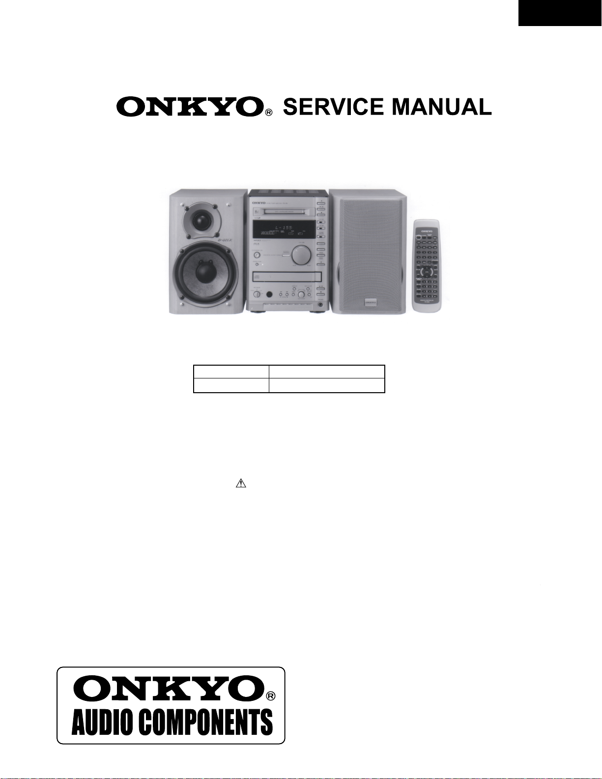
CD/MD TUNER AMPLIFIER
MODEL FR-155
FR-155
Ref. No. 3662
092000
Silver model
UDT
UGT
SAFETY-RELATED COMPONENT WARNING!!
COMPONENTS IDENTIFIED BY MARK ON THE
SCHEMATIC DIAGRAM AND IN THE PARTS LIST ARE
CRITICAL FOR RISK OF FIRE AND ELECTRIC SHOCK.
REPLACE THESE COMPONENTS WITH ONKYO
PARTS WHOSE PART NUMBERS APPEAR AS SHOWN
IN THIS MANUAL.
MAKE LEAKAGE-CURRENT OR RESISTANCE
MEASUREMENTS TO DETERMINE THA T EXPOSED
PARTS ARE ACCEPTABLY INSULATED FROM THE
SUPPLY CIRCUIT BEFORE RETURNING THE
APPLIANCE TO THE CUSTOMER.
120V AC, 60Hz
220 -230V AC, 50/60Hz
TABLE OF CONTENTS
Specifications ----------------------------------------------------------Caution on replacement of optical pickup ---------------------------
Protection of eyes from laser beam during servicing ---------------
Laser W arning Label----------------------------------------------------
Service procedures -----------------------------------------------------
Front panel view --------------------------------------------------------
Connecting to Other Components------------------------------------
Remote controller -------------------------------------------------------
Setting the day of the Week and the Time----------------------------
IC Block diagram and descriptions -----------------------------------
Microprocessor Connection Diagram---------------------------------
Microprocessor Terminal Description--------------------------------
Operation of the Microprocessor--------------------------------------
MD Mechanism Exploded view-------------------------------------
MD Mechanism Disassembly ----------------------------------------
MD Mechanism Reassembly ----------------------------------------
MD Adjustment Procedures ------------------------------------------
MD Mount View / Messages--------------------------------------------
CD Mechanism Exploded View ---------------------------------------
CD Adjustment Procdedure-------------------------------------------
Clock Adjustment Procdedure-----------------------------------------
Handling of Pickup-----------------------------------------------------
Chassis Exploded View Parts List------------------------------------
Chassis Exploded View ------------------------------------------------
Block Diagram----------------------------------------------------------
Block Diagram (Power Supply Section)------------------------------
Schematic Diagram (Amplifire Section)-----------------------------
Printed Circuit Board View 1------------------------------------------
Schematic Diagram (CD&Microprocessor Section)----------------
Printed Circuit Board View 2------------------------------------------
Schematic Diagram (Power Supply Section)-----------------------
Printed Circuit Board View 3------------------------------------------
Printed Circuit Board View Parts List--------------------------------
Wiring V ie w-------------------------------------------------------------
Packing View Parts List------------------------------------------------
2
2
3
3
3
4
5
6
6
7
15
16
17
18~19
20,21
22
23~25
26
27,28
29
30
31
32
33
35
37
39
41
43
45
47
49
51~54
55
57
Page 2

FR-155
SPECIFICATIONS
General
Power supply AC 220-230 V, 50/60 Hz
AC 120 V, 60 Hz
Power consumption 63 W (220-230 V, 50/60 Hz)
82 W (120 V, 60 Hz)
(Standby) 7 W
(Energy Save) 1.5 W
Clock precision
Dimensions (W × H × D) 205 × 154 × 356 mm
Weight 5.5 kg, 12.1 lbs
Amplifier
Power output
Dynamic power 2 × 23 W at 4 W
Total harmonic distortion 0.4 % at rated power
IM distortion 0.2 % at rated power
Damping factor 25 at 8 Ω
Sensitivity and impedance LINE, TAPE:
Frequency response 10 to 50,000 Hz : +0dB / -3 dB
Tone Control S.BASS1: +4 dB at 40 Hz
Signal to noise ratio
Muting
CD player
Signal readout system Optical non-contact
Frequency response 10 Hz to 20 kHz ( 3 dB)
Wow and flutter Below threshold of
monthly error: 30 seconds
(at 25 degrees Celsius)
8-1/16" × 6-1/16"× 14"
2 × 26 W at 4 W EIAJ
2 × 21 W at 6 W EIAJ
Rated Power
2 × 19 W min, RMS at 4 W
1 kHz no more than
0.2 % THD
150 mV, 50 kW
CDR: 150 mV, 50 kW
S.BASS2: +8 dB at 50 Hz
S.BASS3: +4 dB at 10 kHz/
+8 dB at 50 Hz
LINE, CDR, TAPE: 100dB
(IHF-A)
50 dB
measurability
MD recorder
Signal readout system Optical non-contact
Recording time 320 minutes maximum
(at LP4 mode)
Frequency response 10 Hz to 20 kHz ( 3 dB)
Wow and flutter Below threshold of
measurability
Tuner
Tuning range FM: 87.50 to 108.00 MHz
(50 kHz steps)
AM: 522 to 1611 kHz
(9 kHz steps)
Usable sensitivity FM Mono:11.2 dBf,
1.0 µV (75 W IHF)
Stereo:17.2 dBf,
2.0 µV (75 W IHF)
AM: 30 µV
50 dB quieting sensitivity
Capture ratio 2.0 dB
Image rejection ratio FM: 85 dB
IF rejection ratio FM: 90 dB
Signal to noise ratio FM Mono : 73 dB IHF
Selectivity FM: 50 dB
Harmonic distortion FM: Mono: 0.7 %
Frequency response FM:
Stereo separation FM: 40 dB at 1,000 Hz
Specifications and features are subject to change without noitce.
FM Mono:17.2 dBf,
2.0 µV (75 W)
Stereo:37.2 dBf,
20.0 µV (75 W)
AM: 40 dB
AM: 40 dB
Stereo : 67 dB IHF
AM: 40 dB
( 300 kHz at 40 kHz devi.)
Stereo: 0.3 %
AM: 0.7 %
30 to 15,000 Hz ( 1.5 dB)
FM:
30 dB at 100 to 10,000 Hz
CAUTION ON REPLACEMENT OF OPTICAL PICKUP
The laser diode in the optical pickup block is so sensitive to
static electricity, surge current and etc., that the components
are liable to be broken down or its reliability remarkably
deteriorated.
PRECAUTIONS
1.Ground for the work-desk.
Place a conductive sheet such as a sheet of copper
(with impedance lower than 10 Mohm) on the workdesk and place the set on the conductive sheet so that
the chassis can be grounded.
2.Grounding for the test equipments and tools.
Test equipments and toolings should be grounded in
order that their ground level is the same the ground of
the power source.
During repair,carefully take the following precautions.
(The following precautions are included in the service
parts.)
3. Grounding for the human body.
Be sure to put on a wrist-strap for grounding whose
other end is grounded.
Be particularly careful when the workers wear
synthetic fiber clothes, or air is dry.
4. Select a soldering iron that permits no leakage and
have the tip of the iron well-grounded.
5. Do not check the laser diode terminals with the
probe of a circuit tester or oscilloscope.
2
.
Page 3
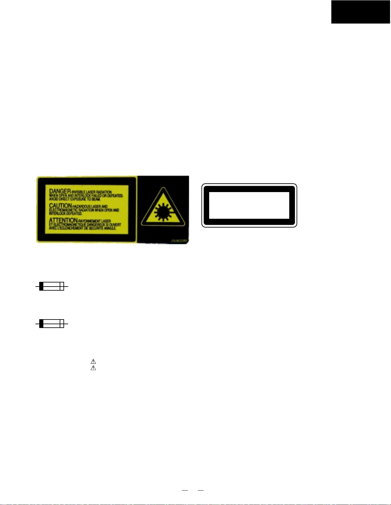
PROTECTION OF EYES FROM LASER BEAM DURING SERVICING
FR-155
This set employs a laser. Therefore, be sure to follow carefully
the instructions below when servicing.
WARNING!!
SERVICE WARNING : DO NOT APPROACH THE
LASER EXIT WITH THE EYE TOO CLOSELY.
IN CASE IT IS NECESSARY TO CONFIRM LASER
BEAM EMISSION, BE SURE TO OBSERVE FROM
A DISTANCE OF MORE THAN 30cm FROM THE
SURFACE OF THE OBJECTIVE LENS ON THE
OPTICAL PICK-UP BLOCK.
LASER WARNING LABEL
The label shown below are affixed.
1. Warning label
Laser Diode Properties
Material: GaAS/GaALAs
Wavelength: 780nm
Laser output: max. 0.5mW*
Emission Duration: continuous
*This output is the value measured at a distance about 1.8mm
from the objective lens surface on the Optical Pick-up Block.
2. Class 1 label
LUOKAN 1
LASERLAITE
"CLASS 1 LASER
PRODUCT"
KLASS 1
LASER APPARAT
SERVICE PROCEDURE
1. Replacing the fuses
This symbol located near the fuse indicates that the
fuse used is show operating type, For continued protection against
fire hazard, replace with same type fuse , For fuse rating, refer to
the marking adjest to the symbol.
Ce symbole indique que le fusible utilise est e lent.
Pour une protection permanente, n'utiliser que des fusibles de meme
type. Ce demier est indique la qu le present symbol est apposre.
REF.NO.
F901
PART NO.
252157
252083
NOTE : <DT> : 120 V model only
<GT> : 220 V~230 V model only
2. To initialize the unit
1. Press and the hold down the CD STOP button , then press the
STANDBY/ON button.
2. After " All lighting " is displayed, the preset memory and each
mode stored in the memory, are initialized and will return to the
factory settings.
3. Press the STANDBY/ON button.
4. Unplug the AC plug from the wall outlet.
DESCRIPTION
1.25A-UL/T-237, Fuse <DT>
0.4A-SE-EAW, Fuse <GT>
3. Safety-check out
(Only U.S.A. model)
After correcting the original service problem perform the
follwing safety check before releasing the set to the customer
Connect the insulating-resistance tester between the plug of
power supply cord and terminal GND on the back panel.
Specifications: More than 10Mohm at 500V
4. Memory Preservation
This unit does not require memory preservation batteries. A built-in
memory power back-up system preserves the contents of the
memory during power failures and even when the unit is un-plugged.
The unit must be plugged in order to charge the back-up
system.
The memory preservation period after the unit has been unplugged
varies depending on climate and placement of the unit. On the
average, memory contents are protected over a period of a few
weeks after the last time the unit has been unplugged. This period
is shorter when the unit is exposed to a highly humid climate.
5. Changing the AM band step
With the exception of the worldwide models, a tuning step selector
switch is not provided. When you change the band step, change
the parts as shown below.
To 10kHz To 9kHz
R748 open 1 kohms
R749 1 koms open
R748 and R749 on the microprocessor PC board (NADG-6933)
3
Page 4
FR-155
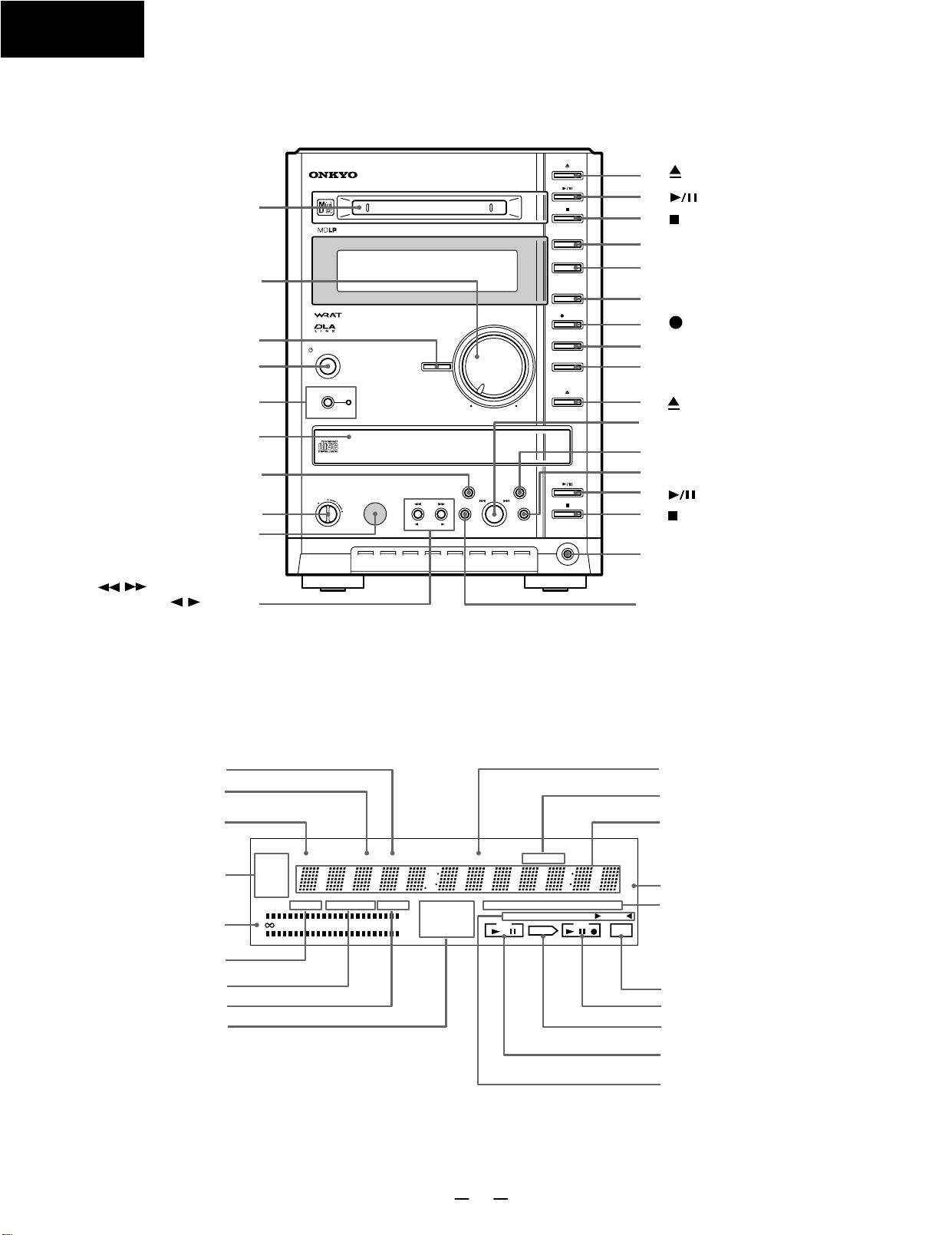
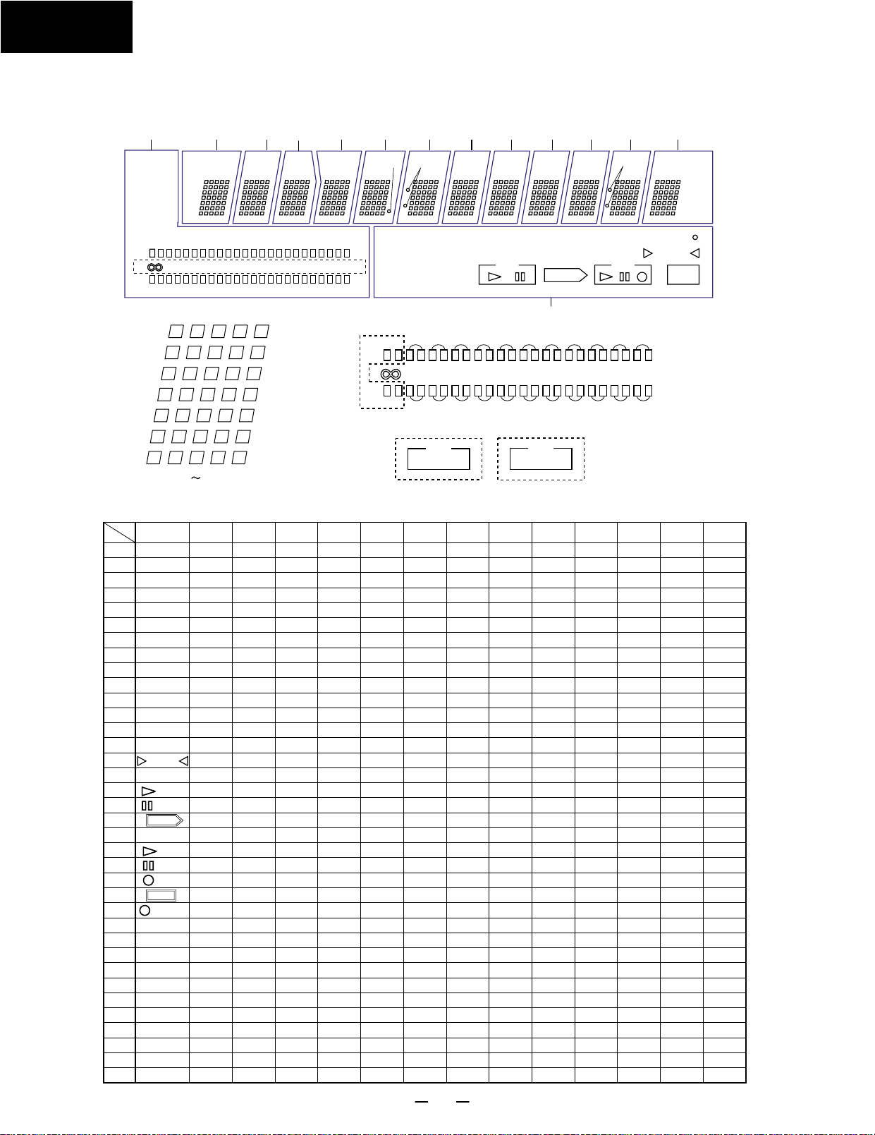
FRONT PANEL VIEW
MD disc slot
VOLUME control
ACOUSTIC
STANDBY/ON button
ENERGY SAVE button
REC MODE switc
Remote control sensor
PRESENCE
/indicator
CD disc tray
DISPLAY button
MD
CD/ MD TUNER AMPLIFIER
DISC LOADING MECHANISM
CD/ MD
FM/AM
button
MD
MD
button
button
CD/MD button
FM/AM button
OTHER
STANDBY/ON
ENERGY SAVE
WIDE RANGE AMPLIFIER
TECHNOLOGY
DISCRETE OUTPUT STAGE
ACOUSTIC
PRESENCE
VOLUME
MIN MAX
INPUTS
REC
CD DUBBING
MODE
AUTO/ MONO
OTHER INPUTS button
MD
REC button
CD DUBBING button
MODE button
AUTO/MONO button
button
CD
MULTI JOG dial
EDIT/CLEAR/NO button
REPEAT/YES button
CD
button
CD button
MULTI JOG
PUSH TO ENTER
EDIT/ CLEAR
REPEAT
NO
YESTUNING
PHONES
REC MODE
SP
LP2
MONO
h
LP4
DISPLAY
TIMER
PHONES jack
/ buttons
TUNING / buttons
DISPLAY
TIMER indicator
CD indicator
SOURCE indicator
Timer indicators
Recording level indicator
MUTING indicator
LEVEL-SYNC indicator
DIGITAL indicator
Playback mode indicators
SLEEP
SOURCE CD TIMER MD MDCHCD
ONCE
W.DAY
W.END
REC
MUTING
L
- 40 - 20 -10 0 OVER- 6 - 2-
R
LEVEL-SYNC DIGIT AL
CHAIN
REPEAT
1 TR MEMOR Y
RANDOM
DISC TRA CK ELAPSED REMAIN TITLE
CD MD
DUB
TUNEDSTEREOAUTOMONO
TIMER button
TOC
MD indicator
MD/CD setting indicator
Multi-purpose displa
s
y
CH (channel) indicator
When lit, the indicators show
what the mulit-purpose display
( Multi-purpose display) above
them is currently displaying.
TOC indicator
MD operation indicators
DUB indicator
CD operation indicators
Indicators for radio frequency
information
4
Page 5
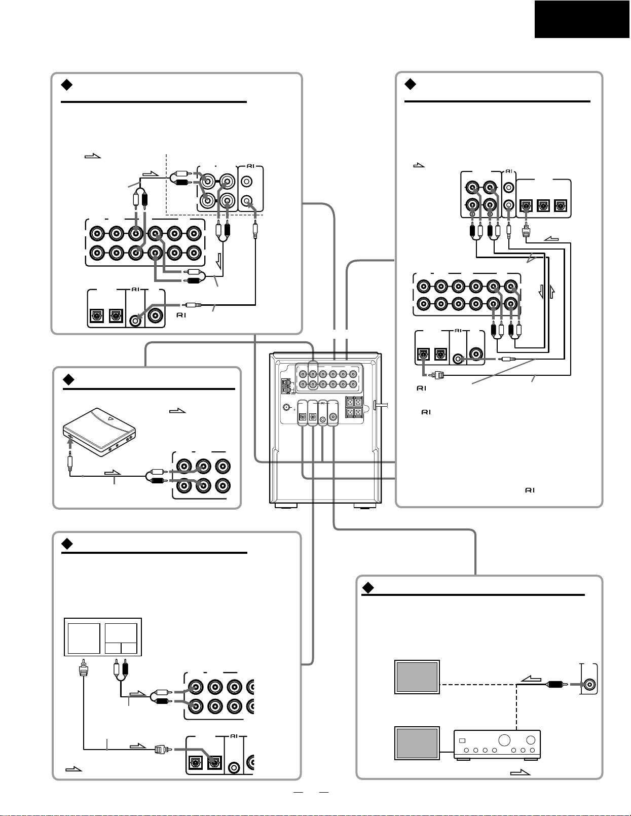
CONNECTING TO OTHER COMPONETS
FR-155
Connecting an Onkyo stereo
cassette tape deck
The illustration below describes the connections to an Onkyo stereo
cassette tape deck.
TAPE OUT (REC) and IN (PLAY) jacks of the unit to the INPUT (REC) and
OUTPUT (PLAY) jacks of the cassette tape deck, respectively.
Audio
connection
cable
LINE-1 LINE-2 TAPE
L
R
FR-155's rear panel
DIGITAL
OUT IN
OPTICAL
To connect to another cassette tape deck, connect the
Onkyo stereo cassette
: Signal flow
tape deck rear panel
INPUT OUTPUT
white
(REC) (PLAY)
L
red
R
OUT IN OUT IN
(
REC)(PLAY
WOOFER
REMOTE
CONTROL PRE OUT
CDR
)(
)
REC
SUB
cable supplied with
the Onkyo stereo
cassette tape deck
L
R
)(
PLAY
Audio connection
cable
REMOTE
CONTROL
Connecting a portable MD player
Refer to the portable MD playerÕs Instruction Manual.
: Signal flow
Audio
connection
cable
white
red
LINE-1 LINE-2 T
L
R
OUT
(
REC
ANTENNA
Rear Panel View
LINE-1 LINE-2 TAPE
OUT IN OUT IN
L
R
AM
(
REC)(PLAY
CAUTION: SPEAKER IMPEDANCE
4 OHMS MIN./ SPEAKER
DIGITAL
SUB
WOOFER
OUT IN
REMOTE
FM
CONTROL PRE OUT
75
OPTICAL
CDR
)(
)
PLAY)(REC
SPEAKERS
L
R
Connecting an Onkyo compact
disc recorder
The following diagram shows how to connect an
optional Onkyo compact disc recorder to the FR-155.
Connect its CDR OUT (REC) jacks and IN (PLA Y)
jacks to the disc recorderÕs INPUT (REC) jacks and
OUTPUT (PLAY) jacks respectively.
: Signal flow
LINE-1 LINE-2 TAPE
L
R
FR-155's rear panel
DIGITAL
OUT IN
OPTICAL
L
R
+–
+–
cable that comes
An
with the compact disc recorder
jack connection enables you to use the
The
following functions:
ANALOG
INPUT
OUTPUT
(REC)
L
R
K
red
white
Audio connection cable
OUT IN OUT IN
(
)(
REC)(PLAY
SUB
WOOFER
REMOTE
CONTROL PRE OUT
¥ You can control a connected Onky o compact disc
recorder from the FR-155' s remote controller.
¥ When the connected Onkyo compact disc recorder
plays bac k, the Input Selector on the FR-155 is
automatically switched to CD-R.
¥ To connect both CD recorder and a cassette tape
deck to the FR-155, connect the
both devices.
Jacks on the compact disc
recorder's rear panel
REMOTE
CONTROL
(PLAY)
L
REC
INPUT1 INPUT2
L
R
CDR
L
R
)(
)
PLAY
Optical fiber audio cable
DIGITAL
OPTICAL
OUTPUT
connectors of
Connecting a DVD player
In addition to the optical digital audio connections,you must also
make analog connections.To connect to the Onkyo DVD player, be
sure to connect to the LINE-1 jacks with the audio connection cable,
not the LINE-2 jacks.
DVD player
Digital
audio
output
Analog
audio output
L R
Audio connection
cable
Optical fiber
audio cable
: Signal flow
FR-155's rear panel
white
L
R
red
LINE-1 LINE-2 TAPE
DIGITAL
OUT IN
OPTICAL
OUT
(
REC)(PL
REMOTE
CONTROL PR
S
WO
Connecting a subwoofer
The FR-155 has a SUBWOOFER PRE OUT jack. Connect
an active subwoofer (a subwoofer that contains an amplifier),
or connect an amplifier to the FR-155, then connect a nonactive subwoofer to the amplifier.
Active subwoofer
(with a built-in amplifier)
SUB
WOOFER
PRE OUT
Subwoofer
(without a built-in amplifier)
Amplifier
: Signal flow
5
Page 6
FR-155
REMOTE CONTROLLER
STANDBY/ON button
CDR/TAPE/LINE/DIGITAL buttons
CD button
MD button
Number buttons
/TAPE REW button
MUTING button
button
MODE button
REPEAT button
CLEAR button
SCROLL button
STANDBY/ON SLEEP
TAPE REW
CD/MD/CDR
REPEAT
CLEAR
SCROLL
CLOCK
CALL
CDR TAPE LINE1 LINE2
CD MD FM AM
1 2 3 4
9 10/0 --/---
M
E
U
L
U
O
P
V
MUTING
V
N
O
L
W
U
O
M
E
D
MODE
REMOTE CONTROLLER
RC-434S
DIGITAL
INPUT
8765
A.PRESENCE
TAPE FF
CD
MD
CDR
TAPE
SLEEP button
CLOCK CALL button
FM/AM buttons
A.PRESENCE button
/TAPE FF button
VOLUME
/ buttons
button
CD operation buttons
MD operation buttons
Operation buttons for an Onkyo CDR
Operation buttons for an
Onkyo stereo cassette tape
dec
k
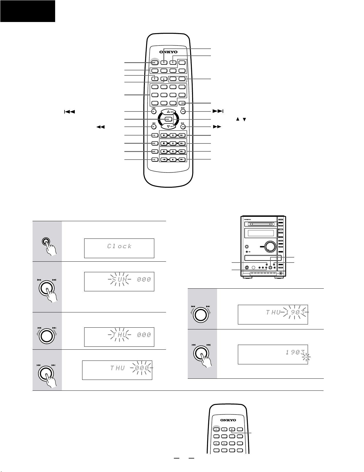
SETTING THE DAY OF THE WEEK AND THE TIME
You can select either the 12-hour display or
to set the time based on the 24-hour display.)
1
TIMER
2
MULTI JOG
PUSH TO ENTER
3
MULTI JOG
PUSH TO ENTER
4
MULTI JOG
PUSH TO ENTER
Press TIMER repeatedly
"Clock"
appears in the display.
SLEEP SOURCE C D TIMER M D M DCHC D
ONCE
W.DAY
W.END
REC
S.BASS
MUTING DIGITAL CHAIN
LEVEL - SYNC
L
-40-20-
-
10 0 OVER-6-2
R
Press MULTI JOG.
SLEEP SOURCE C D TIMER M D M DCHC D
ONCE
W.DAY
W.END
REC
S.BASS
MUTING DIGITAL CHAIN
LEVEL - SYNC
L
-40-20-
-
10 0 OVER-6-2
R
You can now set the day of the week.
If you prefer the 12-hour display, press
DISPLAY.
Turn MULTI JOG to select the
current day of the week.
SLEEP SOURCE C D TIMER M D M DCHC D
ONCE
W.DAY
W.END
REC
S.BASS
MUTING DIGITAL CHAIN
LEVEL - SYNC
L
-40-20-
-
10 0 OVER-6-2
R
Press MULTI JOG to confirm the
SLEEP SOURCE C D TIMER M D M DCHC D
ONCE
W.DAY
W.END
REC
S.BASS
MUTING DIGITAL CHAIN
LEVEL - SYNC
L
-40-20-
-
10 0 OVER-6-2
R
You can now set the time .
REPEAT
1 TR MEMORY
RANDOM
REPEAT
1 TR MEMORY
RANDOM
REPEAT
1 TR MEMORY
RANDOM
REPEAT
1 TR MEMORY
RANDOM
until
DISC TRACK ELAPSED REMAIN TITLE
RDS MONO AUTO STEREO TUNED
M D
C D
DUB TOC
DISC TRACK ELAPSED REMAIN TITLE
RDS MONO AUTO STEREO TUNED
M D
C D
DUB TOC
DISC TRACK ELAPSED REMAIN TITLE
RDS MONO AUTO STEREO TUNED
M D
C D
DUB TOC
DISC TRACK ELAPSED REMAIN TITLE
RDS MONO AUTO STEREO TUNED
C D
M D
DUB TOC
setting.
24-hour displa
DISPLAY
5
MULTI JOG
PUSH TO ENTER
6
MULTI JOG
PUSH TO ENTER
To cancel the clock setting
Press EDIT/CLEAR /NO.
y. (This section
explains how
1
Turn MULTI JOG to set the current
(This example
shows the 24-hour display.)
SLEEP SOURCE C D TIMER M D M DCHC D
ONCE
W.DAY
W.END
REC
LEVEL - SYNC
S.BASS
MUTING DIGITAL CHAIN
L
-40-20-
-
10 0 OVER-6-2
R
REPEAT
1 TR MEMORY
RANDOM
DISC TRACK ELAPSED REMAIN TITLE
RDS MONO AUTO STEREO TUNED
C D
Press MULTI JOG in sync with
signal.
SLEEP SOURCE C D TIMER M D M DCHC D
ONCE
W.DAY
W.END
REC
LEVEL - SYNC
S.BASS
MUTING DIGITAL CHAIN
L
-40-20-
-
10 0 OVER-6-2
R
The clock starts operating and a dot
indicating seconds starts to flash.
REPEAT
1 TR MEMORY
RANDOM
DISC TRACK ELAPSED REMAIN TITLE
RDS MONO AUTO STEREO TUNED
C D
2-6
EDIT/
CLEAR/NO
M D
DUB TOC
the time
M D
DUB TOC
time
.
Checking the time and the day of the week
To check the time and the day of the week, press
TIMER to display "Clock, then press DISPLAY.The
display now indicates the day of the week and the
current time.Alternatively,press CLOCK CALL on the
remote controller. To switch between the 12-hour and
24-hour displays,press DISPLAY while the current time
is indicated on the display.
STANDBY/ON SLEEP
CLOCK
CALL
DIGITAL
CDR TAPE LINE1 LINE2
CD MD FM AM
1 2 3 4
INPUT
CLOCK CALL
6
Page 7
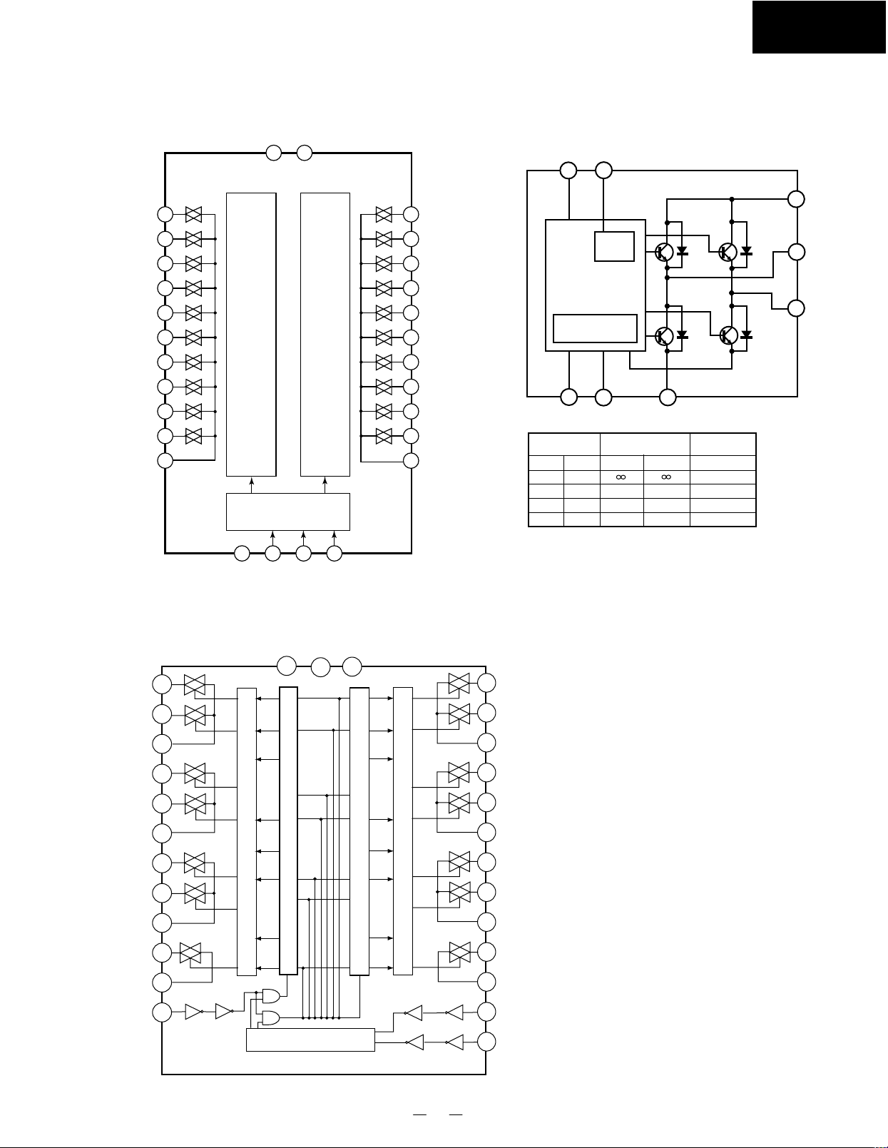
I C BLOCK DIAGRAM AND DESCRIPTIONS
FR-155
Q401:TC9273N-004 (Analog function switch)
VSS
VDD
128
2
S1
S2
S3
S4
S5
S6
S7
S8
S9
S10
OUT
10
11
12
3
4
5
6
7
8
9
10BITS LATCH CIRCUIT
LEVEL SHIFT AND
SHIFT REGISTER
13 14 15 16
GND CK DATA STB
10BITS LATCH CIRCUIT
27
26
25
24
23
22
21
20
19
18
17
S1
S2
S3
S4
S5
S6
S7
S8
S9
S10
OUT
Q103,Q181:TA7291S (Motor driver)
Vref
Vcc
2
8
REG
PROTECTOR
159
IN1 IN2 GND
INPUT
IN1
IN2
0
1
0
1
CCW : Counter clockwise direction
CW : Clockwise direction
OUTPUT
OUT1
0
0
1
1
OUT2
MODE
STOP
H
H
L
L
H
L
CW/CCW
CCW/SW
BRAKE
6
7
3
Vss
OUT1
OUT2
Q447:TC9162AN (Analog function switch)
S1
S2
S3
COM1
S4
S5
S6
COM2
S7
S8
COM3
ST
12
13
10
11
VSS
1
2
3
4
5
6
7
8
9
LATCH CIRCUIT
LEVEL SHIFTER
SHIFT REGISTER
GND
14
VDD
28
LATCH CIRCUIT
LEVEL SHIFTER
27
26
25
24
23
22
21
20
19
18
17
16
15
S1
S2
S3
COM1
S4
S5
S6
COM2
S7
S8
COM3
DATA
CK
7
Page 8
FR-155
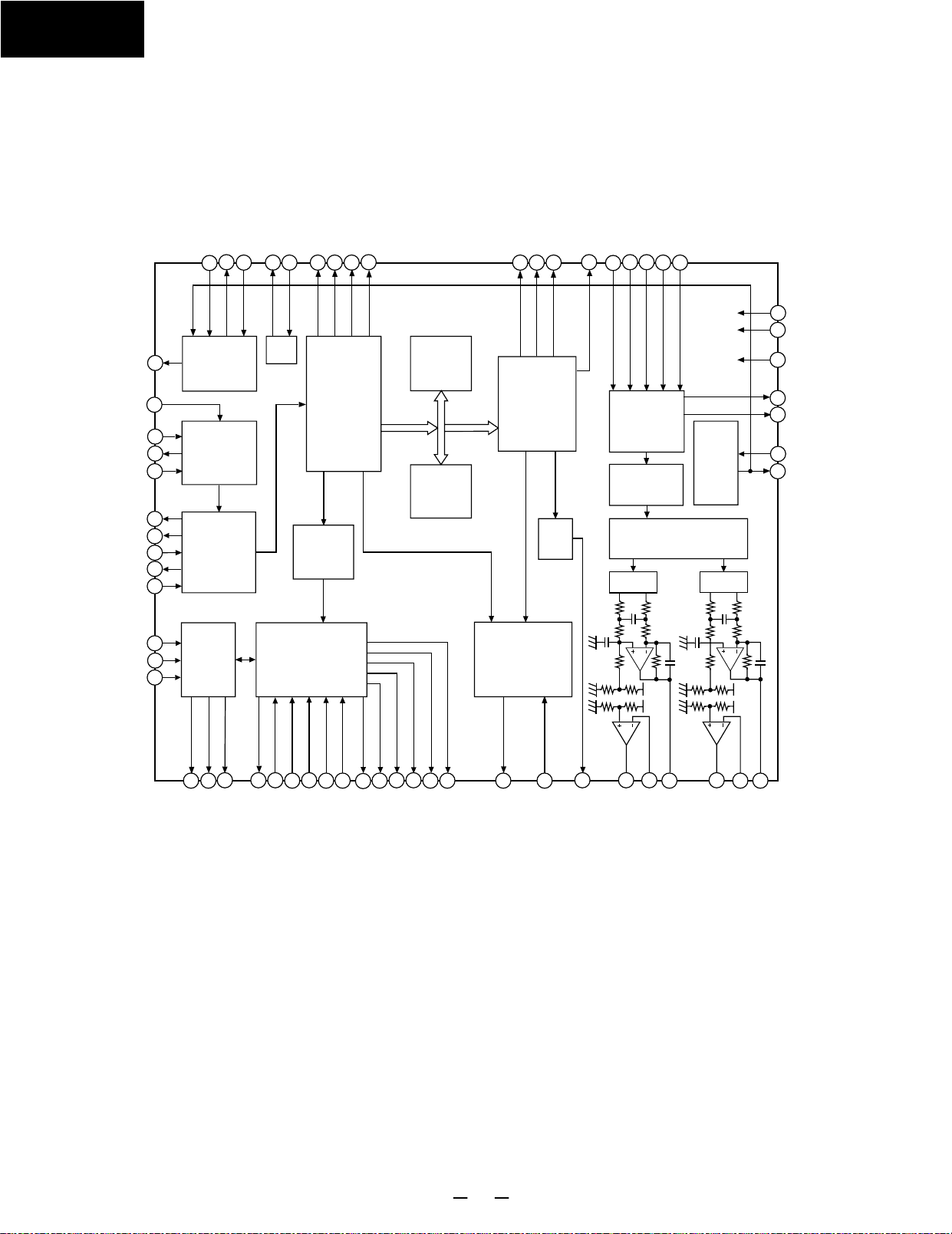
Q351:CXD2589Q (CD Digital Signal Processor)
Block Diagram
XTSL
VPCO
VCKI
V16M
VCTL
XUGF
GFS
EMPH
49
EFM
WFCK
56
54
C4M
RF
ASYI
ASYO
BIAS
XPCK
FILO
FILI
PCO
CLTV
52
52
35
35
37
37
38
36
36
48
48
30
30
31
31
29
29
33
38
33
51
51 25 26 27 28 47 49 54 56 50 39 41 43 55 40 42 44 62
25
Clock
28
26
47
27
OSC
Generator
demodurator
Asymmetry
Corrector
Digital
PLL
Sub Code
Processor
Error
Corrector
16K
RAM
C2PO
LRCK
39
50
D/A
Interface
Digital
OUT
PCMD
41
BCK
EMPHI
LRCKI
40
424344
55
Serial-In
Interface
Over Sampling
Digital Filter
Noise Shaper
PWM
PCMDI
BCKI
SYSM
62
3rd-Order
Timing
Logic
PWM
24
24
23
23
79
79
70
70
71
71
3
3
2
2
TES1
TEST
XRST
RMUT
LMUT
XTAI
XTAO
FOK
SEIN
CNIN
18
18
10
10
11
11
Servo
Auto
Sequencer
12 13 14 6 7 8 9 15 16 17 57 58 59 5 4 21 22 53 74 75 76 67 66 65
14
13
12
DATO
CLKO
XLTO
CPU
Interface
65
7
SENS
DATA
XLAT
15 16 17
CLOK
SPOA
XLON
SPOB
57
58
SCOR
9
8
59
EXCK
SBSO
4
SQCK
SQSO
Digital
CLV
21
MDP
22
53
PWMI
DOUT
74
LOUT2
75
76
AIN2
AOUT2
67
LOUT1
66
65
AIN1
AOUT1
8
Page 9
PIN Description
Pin
No.
1
2
3
4
5
6
7
8
9
10
11
12
13
14
15
16
17
18
19
20
21
22
23
24
25
26
27
28
29
30
31
32
33
34
35
36
37
38
39
40
41
42
Symbol
VSS
LMUT
RMUT
SQCK
SQSO
SENS
DATA
XLAT
CLOK
SEIN
CNIN
DATO
XLTO
CLKO
SPOA
SPOB
XLON
FOK
VDD
VSS
MDP
PWMI
TEST
TES1
VPCO
VCKI
V16M
VCTL
PCO
FILO
FILI
AVSS
CLTV
AVDD
RF
BIAS
ASYI
ASYO
LRCK
LRCKI
PCMD
PCMDI
I/O
GND
—
Left-channel zero detection flag.
O
Right-channel zero detection flag.
O
SQSO readout clock input.
I
Sub Q 80-bit serial output.
O
SENS output to CPU.
O
Serial data input from CPU.
I
Latch input from CPU. Serial data is latched at the
I
falling edge.
Serial data transfer clock input from CPU.
I
SENS input from SSP.
I
Track jump count signal input.
I
Serial data output to SSP.
O
Serial data latch output to SSP. Latched at the falling
O
edge.
Serial data transfer clock output to SSP.
O
Microcomputer extended interface (input A).
I
Microcomputer extended interface (input B).
I
Microcomputer extended interface (output).
O
Focus OK input.
I
Used for SENS output and the servo auto sequencer.
Power supply (+5V).
—
GND
—
Spindle motor servo control.
O
Spindle motor external control input.
I
TEST pin; normally GND.
I
TEST pin; normally GND.
I
Charge pump output for the wide-band EFM PLL.
O
VCO2 oscillation input for the wide-band EFM PLL.
I
VCO2 oscillation output for the wide-band EFM
O
PLL.
VCO2 control voltage input for the wide-band EFM
I
PLL.
Master PLL charge pump output.
O
Master PLL (slave = digital PLL) filter output.
O
Master PLL filter input.
I
Analog GND.
—
Master VCO control voltage input.
I
Analog power supply (+5V).
—
EFM signal input.
I
Constant current input of the asymmetry circuit.
I
Asymmetry comparator voltage input.
I
EFM full-swing output (low = VSS, high = VDD).
O
D/A interface. LR clock output f = Fs.
O
LR clock input.
I
D/A interface. Serial data output (two's complement,
O
MSB first).
D/A interface. Serial data input (two's complement,
I
MSB first).
Description
Pin
No.
43
44
45
46
47
48
49
50
51
52
53
54
55
56
57
58
59
60
61
62
63
64
65
66
67
68
69
70
71
72
73
74
75
76
77
78
79
80
Symbol
BCK
BCKI
VSS
VDD
XUGF
XPCK
GFS
C2PO
XTSL
C4M
DOUT
EMPH
EMPHI
WFCK
SCOR
SBSO
EXCK
VSS
VDD
SYSM
AVSS
AVDD
AOUT1
AIN1
LOUT1
AVSS
XVDD
XTAI
XTAO
XVSS
AVSS
LOUT2
AIN2
AOUT2
AVDD
AVSS
XRST
VDD
I/O
D/A interface. Bit clock output.
O
D/A interface. Bit clock input.
I
GND
—
Power supply (+5V).
—
XUGF output. Switched to MNT1 or RFCK output
O
by a command.
XPLCK output. Switched to MNT0 output by a com-
O
mand.
GFS output. Switched to MNT3 or XRAOF output
O
by a command.
C2PO output. Switched to GTOP output by a com-
O
mand.
Crystal selector input. Low: 16.9344MHz;
I
high: 33.8688MHz.
4.2336MHz output. 1/4 frequency-divided VCKI out-
O
put in CAV-W mode.
Digital Out output.
O
Outputs a high signal when the playback disc has
O
emphasis, and a low signal when there is no emphasis.
Inputs a high signal when de-emphasis is on, and a
I
low signal when de-emphasis is off.
WFCK output.
O
Outputs a high signal when either subcode sync S0
O
or S1 is detected.
Sub P to W serial output.
O
SBSO readout clock input.
I
GND
—
Power supply (+5V).
—
Mute input. Active when high.
I
Analog GND.
—
Analog power supply (+5V).
—
Left-channel analog output.
O
Left-channel operational amplifier input.
I
Left-channel LINE output.
O
Analog GND.
—
Power supply for master clock.
Crystal oscillation circuit input. Input the external
I
master clock via this pin.
Crystal oscillation circuit output.
O
GND for master clock.
Analog GND.
—
Right-channel LINE output.
O
Right-channel operational amplifier input.
I
Right-channel analog output.
O
Analog power supply (+5V).
—
Analog GND.
—
System reset. Reset when low.
I
Power supply (+5V).
—
Description
FR-155
9
Page 10
FR-155
Q101:CXA1992BR (RF Signal Processing Servo Amplifier)
Block Diagram
FE-BIAS
V
TEO
LPFI
TEI
ATSC
TZC
TDFCT
VC
FZC
O
RF
M
FE
-
LDON
I
RF
323334353637
VEE
LEVEL S
VEE
MIRR
VCC
LPCL
LPC
TGFL
IIL DATA REGISTER
INPUT SHIFT REGISTER
ADDRESS DECODER
SENS SELECTOR
OUTPUT DECODER
DFCTO IFB1-6
VCC
FS1
FS2
Charge
VEE
8
SRCH
BAL1-4
TOG1-4
up
CP
31
VCC
9
TGU
30
VEE
FS1-4 TG1-2
TG2
10
CB
MIRR
TG2
VCC
DFCT
IIL
TTL
TN1-7 PS1-4
TM3
FSET
11
CC1
DFCT1
FSET
CC2
2829
CC1
12
FOK
27
26
SENS2
IIL
TTL
TTL
IIL
ISET
VCC
VCC
TM4
TM6
TM3
TM5
VEE
VEE
13
O
M
-
TA
TA
25
SENS1
24
C.OUT
23
XRST
22
DATA
XLT
21
CLK
20
LOCK
19
VCC
V
CC
18
ISET
17
16
SL-O
15
SL-M
14
SL-P
TM2
M
-
RFTC
RF SUMMING AMP
FO.BIAS
WINDOW COMP.
RF
FOK
FOH
FOL
TGH
TGL
BALH
BALL
ATSC
TZC
FZC
PD
VEE
APC
LASER POWER CONTROL
IFB5
IFB3
IFB4
TRK.GAIN
WINDOW COMP
LD
VEE
FE AMP
IFB6
PD1
PD2
3839
PD1 IV
PD2 IV
AMP
AMP
40
41
F
42
E
EI
43
EE
44
F IV AMP
E IV AMP
BAL1
BAL2
BAL3
TOG2
TOG3
BAL4
TOG4
VEE
TOG1
TGFL
VCC
VCC
IFB2
IFB1
VEE
45
E-F BALANCE
46
WINDOW COMP.
47
48
ATSC
WINDOW
COMP.
TZC COMP.
49
50
VCC
DFCT
TM1
TG1
TRACKING
PHASE COMPENSATION
51
VCC
VEE
52
FZC COMP.
12
FEI
FEO
FOCUS
PHASE COMPENSATION
DFCT
FS4
45
3
FDFCT
FGD
FLB
6
7
O
-
FE
10
Page 11
Pin Description
Pin
Symbol
No.
1 FEO O
2 FEI Focus error input. I
34FDFCT
FGD I
5 FLB
6 FE_O
7 FE_M
8 SRCH
9
TGU
10 TG2
11
FSET
12 TA_M I Tracking amplifier inverted input.
TA_O
13
14
SL_P
15 SL_M
16 SL_O O Sled drive output.
17 ISET I Connect an external capacitance to set the current
18
VCC
19 LOCK I
20 CLK
XLT
21
22 DATA
XRST I Reset input; resets at Low. (no pull-up resistance)
23
24 C. OUT
SENS1
25
I/O
Focus error amplifier output.
Connected internally to the window comparator input
for bias adjustment.
I
Capacitor connection pin for defect time constant.
Ground this pin through a capacitor for cutting the
focus servo high-frequency gain.
External time constant setting pin for boosting the
I
focus servo low-frequency.
O
Focus drive output.
I Focus amplifier inverted input.
I
External time constant setting pin for generating
focus search waveform.
I External time constant setting pin for switching track-
ing high-frequency gain.
External time constant setting pin for switching track-
I
ing high-frequency gain.
Peak frequency setting pin for focus and tracking
I
phase compensation amplifier.
O Tracking drive output.
I Sled amplifier non-inverted input.
I Sled amplifier inverted input.
which determines the Focus search, Track jump, and
Sled kick heights.
I Positive power supply.
The sled overrun prevention circuit operates when
this pin is Low. (no pull-up resistance)
I
Serial data transfer clock input from CPU.
(no pull-up resistance)
I
Latch input from CPU. (no pull-up resistance)
Serial data input from CPU. (no pull-up resistance)
I
O
Track number count signal output.
O
Outputs FZC, DFCT1, TZC, BALH, TGH, FOH,
ATSC, and others according to the command from
CPU.
Description
FR-155
Pin
Symbol
No.
26 SENS2 O
27
FOK
28
CC2 I
CC1
29
30 CB I Connection pin for defect bottom hold capacitor.
31 CP
32
RF_I I
33 RF_O O
34 RF_M
35 RFTC I
LD O APC amplifier output.
36
37 PD I APC amplifier input.
PD1
38
39
PD2
40
FE_BIAS
41
F
42IE
43 EI
44
VEE
45 TEO O
46 LPFI I Comparator input for balance adjustment.
47
TEI
ATSC
48
49
TZC
50
TDFCT
51
VC
52 FZC
I/O
Outputs DFCT2, MIRR, BALL, TGL, FOL, and
others according to the command from the CPU.
O Focus OK comparator output.
Input for the defect bottom hold output with capacitance coupled.
O Defect bottom hold output. Connected internally to
the interruption comparator input.
Connection pin for MIRR hold capacitor.
I
MIRR comparator non-inverted input.
Input for the RF summing amplifier output with capa-
citance coupled.
RF sunning amplifier output. Eyepattern check point.
RF summing amplifier inverted input.
I
The RF amplifier gain is determined by the resistance
connected
between this pin and RFO pin.
External time constant setting pin during RF level
control.
I
RF I-V amplifier inverted input. Connect these pins
to the photo diode A + C and B + D pins.
I
I
Bias adjustment of focus error amplifier.
Leave this pin open for automatic adjustment.
I
F I-V and E I-V amplifier inverted input.
Connect these pins to photo diodes F and E.
—
I-V amplifier E gain adjustment.
(When not using automatic balance adjustment)
—
Negative power supply.
Tracking error amplifier output. E-F signal is output.
(Input from TEO through LPF)
Tracking error input.
I
Window comparator input for ATSC detection.
I
I
Tracking zero-cross comparator input.
I
Capacitor connection pin for defect time constant.
O (VCC + VEE)/2 direct voltage output.
I
Focus zero-cross comparator input.
Description
11
Page 12
FR-155
Q102:LA6541D (CD 4-channel BTL Driver )
Vcc
Mute
VIN1
VG1
Vo1
Vo2
GND
GND
GND
Vo3
Vo4
VG2
VI2
Reg OUT
Reg IN
10
11
12
13
14
15
Pin No. Pin Name Description
Vcc
1
2
3
Level shift
1
Level shift
4
4
5
BTL AMP
1
BTL AMP
4
6
30
29
28
27
26
25
Vref
VIN4
VG4
Vo8
Vo7
1
2
3
4
5
6
7
8
9
10
11
12
GND
7
8
Vcc
24
23
GND
13
14
15
16
GND
9
22
17
18
BTL AMP
2
BTL AMP
3
21
20
Vo6
Vo5
19
20
21
22
Level shift
2
Level shift
3
19
18
VG3
VIN3
23
24
25
26
Regulator
RESET
17
16
CD
RES
27
28
29
30
VCC
Mute ON/OFF control for all BTLAMP outputs
VIN1
VG1 BTL AMP 1 input (for gain control)
Vo1
Vo2
GND GND (minimum electric potential)
GND GND (minimum electric potential)
GND GND (minimum electric potential)
V
O
V
O
VG2 BTL AMP 2 input (for gain control)
V
IN
REG OUT Connection for collector of external transistor (PNP); 5 V supply output
REG IN Connection for base of external transistor (PNP)
RES
C
V
IN
VG3 BTL AMP 3 input (for gain control)
V
O
V
O
GND GND (minimum electric potential)
GND GND (minimum electric potential)
GND GND (minimum electric potential)
V
O
V
O
VG4 BTL AMP 4 input (for gain control)
V
IN4
V
REF
V
CC
Power supply (shorted with pin 30)
BTL AMP 1 input
BTL AMP 1 output (non-inverting side)
BTL AMP 1 output (inverting side)
3 BTL AMP 2 output (inverting side)
4 BTL AMP 2 output (non-inverting side)
2 BTL AMP 2 input
Reset output
Reset output delay time setting (with capacitor)
D
3 BTL AMP 3 input
5 BTL AMP 3 output (non-inverting side)
6
BTL AMP 3 output (inverting side)
7 BTL AMP 4 output (inverting side)
8 BTL AMP 4 output (non-inverting side)
BTL AMP 4 input
Reference voltage input for level shift circuit
Power supply (shorted with pin 1)
(Function)
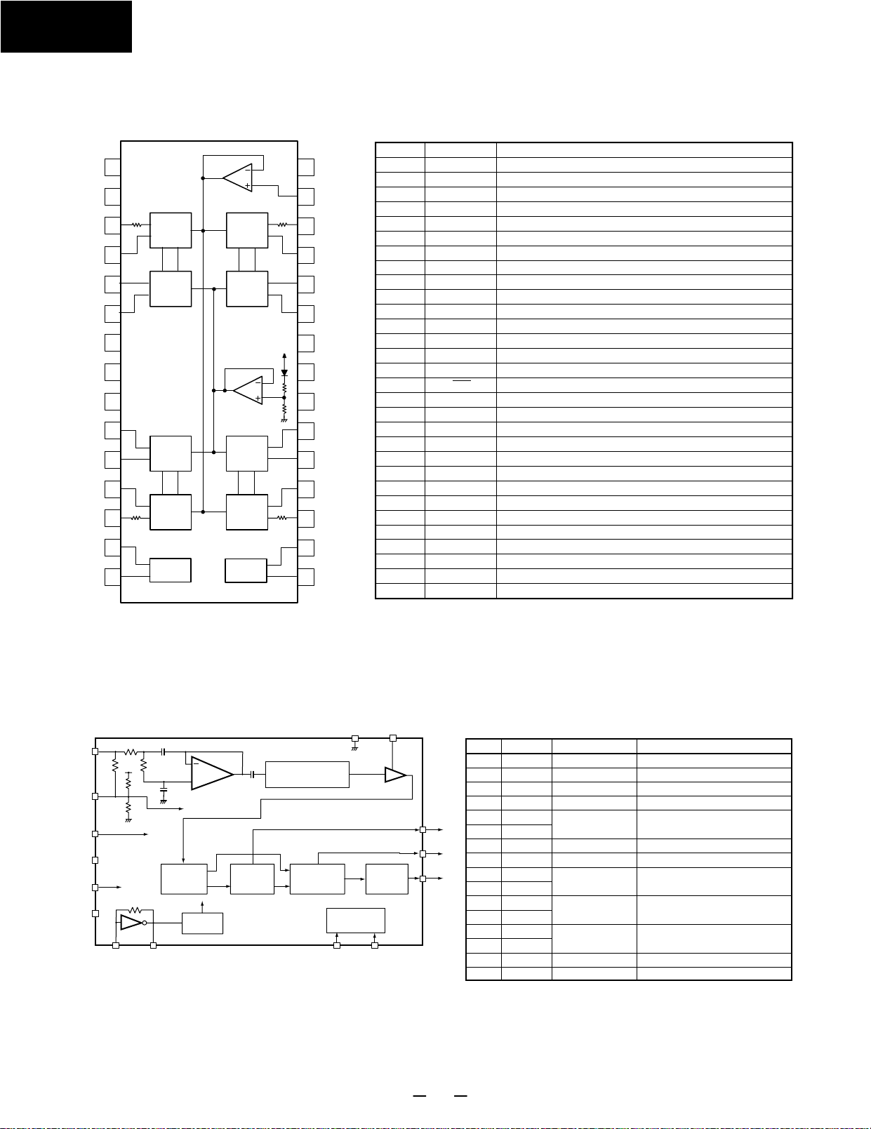
Q171:BU1923(RDS Decoder)
100k
(4)
MUX
VREF
VDD1
VSS1
VDD2
VSS2
120k
(3)
(5)
(6)
(12)
(11)
Analog
Power supply
Digital
power supply
(13) (14)
X1
XO
100k
PLL
57kHz
RDS/ARI
Reference
+
anti-aliasing
filter
clock
PLL
1187.5Hz
capacitor filter
8ch Switched
Bi-phase
decoder
Measurement
(10)
VSS3
circuit
CMP
(7)
Comparator
Differential
decoder
(9)
T2T1
(8)
(16)
(1)
(2)
Pin No.
RCLK
QUAL
RDATA
Symbol
QUAL
1
RDATA
2
3
4
VDD1
5
6
7
8
9
10
VDD2
11
12
13
14
15
RCLK
16
Vref
MUX
Vss1
Vss3
CMP
T2
T1
Vss2
XI
XO
(NC)
Pin name
Demodulator quality
Demodulator data
Reference voltage
Input
Analog power supply
GND
Comparator input
Test input
Digital power supply
Crystal oscillor
-
Demodulator clock
Function
Good data : High , bad data : Low
Refer to output data trimming
1/2 VDD1 (refer to input/output circuits)
Composite signal input
4.5V to 5.5V
C-junction
Open or connected to ground
4.5V to 5.5V
Connects to 4.332MHz oscillator
(refer to input/output circuit)
-
1187.5Hz clock
12
Page 13
Q752:M66004F (FL Tube Driver)
FR-155
Chip select
input
Shift clock
input
Serial data
input
Reset
input
Clock
input
Clock
output
CS
SCK
SDATA
RESET
XIN
XOUT
15
16
13
21
22
14
Serial
receive
circuit
Clock
generator
Display code
register
code
write
Code /
command
control
circuit
Display
control
register
RAM
write
code
select
Display controller
CG ROM
(35bit 160)
Decoder
CG RAM
(35bit 16)
Decoder
Segment
output circuit
Output port
(2bits)
Digit
output circuit
12
59
33
31
23
18
17
1
64
61
SEG00
SEG26
SEG27
SEG35
P0
P1
DIG00
DIG11
DIG12
DIG15
Segment
output
Output
ports
Digit
outputs
Pin No.
13
14
15
16
21,
22
1-12
61-64
23-31
33-59
17,18
19
60
22
32
Symbol Pin name Function
RESET Reset input This pin is used to initialize the internal state on the M66004
CS Chip select input
"L" : communication with the MCU is possible.
"H" : any instruction from teh MCU is neglected.
SCK Shift select input At the rising edge from "L"to"H" , input data is shifted.
SDATA Serial data input Character code or command data to display is input from MSB.
XIN,
XOUT
DIG00 -
Clock input
Clock output
Digit output
Set oscillation frequency
These pins are used to connect to digit pins of VFD.
DIG15
SEG00 -
Segment output
These pins are used to connect to segment pins of VFD.
SEG35
P0,PI Output port (static operation)
VCC1
VCC2
VSS
Positive power supply for internal logic.
Positive power supply for high-pressure-resistant output port.
GND
VP Negative power supply for VFD drive.
13
Page 14
FR-155
Q751:BJ780GNK(FL T ube)
13G 12G 11G 10G 9G 8G 7G 6G 5G 4G 3G 2G 1G
Dp
SLEEP SOURCE C D TIMER M D M DCHC D
ONCE
W.DAY
W.END
REC
S.BASS
MUTING DIGITAL
LEVEL - SYNC
L
-
-
40-20-10 0 OVER
-
S2
-
6
2
R
1-1 2-1 3-1 4-1 5-1
1-2 2-2 3-2 4-2 5-2
1-3 2-3 3-3 4-3 5-3
1-4 2-4 3-4 4-4 5-4
1-5 2-5 3-5 4-5 5-5
1-6 2-6 3-6 4-6 5-6
1-7 2-7 3-7 4-7 5-7
(12G 1G)
(13G)
L
-
R
(14G)
Col-2
CHAIN
REPEAT
1 TR MEMORY
RANDOM
S1
B12 B13 B14 B15 B16 B17 B18 B19 B20 B21 B22
-
40
B1 B2 B3 B4 B5 B6 B7 B8 B9 B10 B11
C D
S3
DISC TRACK ELAPSED REMAIN TITLE
RDS MONO AUTO STEREO TUNED
C D
-
20
-
10 0 OVER
DUB TOC
14G
-
6
M D
S4
Col-1
M D
-
2
14G 13G 12G 11G 10G 9G 8G 7G 6G 5G 4G 3G 2G 1G
P1
P2
P3
P4
P5
P6
P7
P8
P9
P10
P11
P12
P13
P14
P15
P16
P17
P18
P19
P20
P21
P22
P23
P24
P25
P26
P27
P28
P29
P30
P31
P32
P33
P34
P35
P36
CHAIN
REPEAT
1 TR
MEMORY
RANDOM
DISC
TRACK
ELAPSED
REMAIN
TITLE
RDS
MONO
AUTO
STEREO
TUNED
S3
(CD)
(CD)
DUB
S4
(MD)
(MD)
(MD)
TOC
(TITLE)
-
-
-
-
-
-
-
-
-
-
-
B1
B8
B12
B19
S1
B2
B9
B13
B20
S2
B3
B10
B14
B21
OVER
B4
B11
B15
B22
SLEEP
B5
ONCE
B16
W.DAY
W.END
B6
REC
S.BASS
MUTING
B18
LEVEL-SYNC
B7
DIGITAL
-
B17
-
1-1
2-1
3-1
4-1
5-1
1-2
2-2
3-2
4-2
5-2
1-3
2-3
3-3
4-3
5-3
1-4
2-4
3-4
4-4
5-4
1-5
2-5
3-5
4-5
5-5
1-6
2-6
5-7
4-7
3-7
2-7
1-7
5-6
4-6
3-6
SOURCE
1-1
2-1
3-1
4-1
5-1
1-2
2-2
3-2
4-2
5-2
1-3
2-3
3-3
4-3
5-3
1-4
2-4
3-4
4-4
5-4
1-5
2-5
3-5
4-5
5-5
1-6
2-6
5-7
4-7
3-7
2-7
1-7
5-6
4-6
3-6
-
1-1
2-1
3-1
4-1
5-1
1-2
2-2
3-2
4-2
5-2
1-3
2-3
3-3
4-3
5-3
1-4
2-4
3-4
4-4
5-4
1-5
2-5
3-5
4-5
5-5
1-6
2-6
5-7
4-7
3-7
2-7
1-7
5-6
4-6
3-6
CD
1-1
2-1
3-1
4-1
5-1
1-2
2-2
3-2
4-2
5-2
1-3
2-3
3-3
4-3
5-3
1-4
2-4
3-4
4-4
5-4
1-5
2-5
3-5
4-5
5-5
1-6
2-6
5-7
4-7
3-7
2-7
1-7
5-6
4-6
3-6
TIMER
1-1
2-1
3-1
4-1
5-1
1-2
2-2
3-2
4-2
5-2
1-3
2-3
3-3
4-3
5-3
1-4
2-4
3-4
4-4
5-4
1-5
2-5
3-5
4-5
5-5
1-6
2-6
5-7
4-7
3-7
2-7
1-7
5-6
4-6
3-6
Dp
1-1
2-1
3-1
4-1
5-1
1-2
2-2
3-2
4-2
5-2
1-3
2-3
3-3
4-3
5-3
1-4
2-4
3-4
4-4
5-4
1-5
2-5
3-5
4-5
5-5
1-6
2-6
5-7
4-7
3-7
2-7
1-7
5-6
4-6
3-6
col 2
1-1
2-1
3-1
4-1
5-1
1-2
2-2
3-2
4-2
5-2
1-3
2-3
3-3
4-3
5-3
1-4
2-4
3-4
4-4
5-4
1-5
2-5
3-5
4-5
5-5
1-6
2-6
5-7
4-7
3-7
2-7
1-7
5-6
4-6
3-6
MD
1-1
2-1
3-1
4-1
5-1
1-2
2-2
3-2
4-2
5-2
1-3
2-3
3-3
4-3
5-3
1-4
2-4
3-4
4-4
5-4
1-5
2-5
3-5
4-5
5-5
1-6
2-6
5-7
4-7
3-7
2-7
1-7
5-6
4-6
3-6
-
1-1
2-1
3-1
4-1
5-1
1-2
2-2
3-2
4-2
5-2
1-3
2-3
3-3
4-3
5-3
1-4
2-4
3-4
4-4
5-4
1-5
2-5
3-5
4-5
5-5
1-6
2-6
5-7
4-7
3-7
2-7
1-7
5-6
4-6
3-6
MD
1-1
2-1
3-1
4-1
5-1
1-2
2-2
3-2
4-2
5-2
1-3
2-3
3-3
4-3
5-3
1-4
2-4
3-4
4-4
5-4
1-5
2-5
3-5
4-5
5-5
1-6
2-6
5-7
4-7
3-7
2-7
1-7
5-6
4-6
3-6
CD
1-1
2-1
3-1
4-1
5-1
1-2
2-2
3-2
4-2
5-2
1-3
2-3
3-3
4-3
5-3
1-4
2-4
3-4
4-4
5-4
1-5
2-5
3-5
4-5
5-5
1-6
2-6
5-7
4-7
3-7
2-7
1-7
5-6
4-6
3-6
col 1
1-1
2-1
3-1
4-1
5-1
1-2
2-2
3-2
4-2
5-2
1-3
2-3
3-3
4-3
5-3
1-4
2-4
3-4
4-4
5-4
1-5
2-5
3-5
4-5
5-5
1-6
2-6
5-7
4-7
3-7
2-7
1-7
5-6
4-6
3-6
CH
14
Page 15
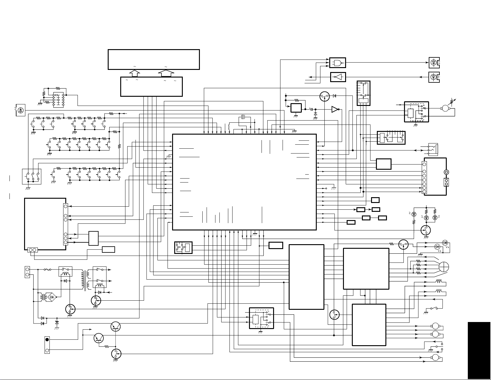
MICROPROCESSOR CONNECTION DIAGRAM
Q751
FL TUBE
REMOTE
SENSOR
15
AC IN
Q753
P907
to POWER
SUPPLY
NAPS-6928
REC MODE SW
ST
LP2
LP4
YES
CD
STOP
CD
PLAY
REC
OTHER
INPUT
CD
EDIT
EJECT
/NO
MULTI JOG
MD MECHANISM
CN105
RC DATA
RC REQ
SHUT DOWN
MD REQ-2
15
MD CLK
F901
P913B
D901
Q901
POWER
16
17
MD RST
MD DATA-2
14 AMOT
15
CN102
RELAY DRIVE
2
5
6
RL901
F.F
MONO
MD
FM
/CDMDSTOPMDPLAY
/AM
ENERGY
SAVE
Q902
POWER
SWITCH
REW
STANDBY
T901
AMP
Q112
M66004F
DISPLAY
A.PRES
RL902
+5.6 V
Q752
FL TUBE
DRIVER
TIMER
MD
EJECT
MODE
Q391
BUFFER
TO POWER AMP
PC BOARD
(NAAF-6930)
+B
1G 14G
1 12,60 64
GRID
+5 V
+5.6 V
CD.DUB
Q203,Q204
MD MUT
Q112
Q112
CD POWER
CONTROL
RESCSSCK
131415
P1 P36
23 31,33 59
SEGMENT
DATA
16
1 ROTEN 2
2 ROTEN 1
3 FLRESET
4 GND
5 SHUT DOWN
6 RCREQ
7 +5 V
8 MD DATA
9 RC DATA
10 S CLK
11 FLCE
12 FL DATA
13 FL CLK
14 TXD
15 RXD
16 SQSO
17 SESN
18 SQCK
19 CD CLK
20 CD DATA
Q222 TC4052BP
REC LEVEL
CONTROL
SIGNAL 80
21 CD XLT
K 2 78
K 1 77
MD REC MODE 79
22 CD RESET
23 CD POWER
24 OPEN
X701 5MHz
+5.6 V
72
K 0 76
+5 V 75
+5 V 74
GND 71
GND 73
Q701
MPD780058GC
MICROPRCESSOR
25 CLOSE
26 AC POWER
27 OPEN SW
28 CLOSE SW
29 SENS 2
30 ECO LED
+5.6 V
IN2
IN1
TRAY MOTOR DRIVER
+5.6 V
+5 V 68
GND 67
CLOCK 70
CLOCK 69
MD REQ 66
31 REC VOL 1
32 REC VOL 2
33 GND
34 RC POWER
35 MD RESET
Q449 POWER
2
1
9
5
Q103 TA7291S
POFF 63
SCOR 65
RDS CLK 64
36 BAND 0
37 BAND 1
38 AM 10K
AMPLIFIRE
CONTROL
3
OUT2
7
OUT1
MD MECHA
AUX-MD IN
A MUTE
MD OUT
+5.6 V
D OUT 62
REMIN 61
39 RD SEN
40
Q705
RESET
IN
OUT
RESET 60
SYS OUT 59
SYS IN 58
VOL DOWN 57
VLO UP 56
RDS DATA 55
RDS SIG 54
PLLCE 53
SD 52
STEREO 51
MODEL 1 50
FREQCAL 49
C DATA 48
C CLK 47
TU MUT 46
FCE/VCE 45
REC MUT 44
AP LED 43
SEL MUT 42
CD MUT 41
9
8
7
Q351
6
CXD2589Q
5
CD DIGITAL
4
SIGNAL
79
PROCESSOR
19
Q704
Q371
TC74HCT00AF
BUFFER
Q372
TC7WU04FU
BUFFER
Q401
TC9273N-004
INPUT
Q703
RESET
SELECTOR
+5.6 V
Q447
TC9162AN
ACOUSTIC
PRESENCE SELECTOR
Q171 BU1923
Q253
TUNER MUTING
Q223,Q224
Q707
MUT
Q448
SEL MUT
Q702
CD MUT
57
Q112
20
21
22
24
25
27
23
26
15
19
30
Q101
CXA1992BR
RF SIGNAL
PROCESSING
SERV O AMP
28 3 13
Q102
LA6541D
FOCUS
/TRACKING
& SLED
/SPINDLE
MOTOR
DRIVER
14
13
12
11
10
18
15
21
MD REC
MUTING
Q443
,Q444
Q114 LD DRIVE
37
36
39
38
41
42
1361615
5
6
10
11
25
26
21
20
Q171
BU1923
VOLUME MOTOR
DRIVER
2
1
IN2
IN1
9
5
RDS
DECODER
ENERGY
SAVE
LED
TUNER UNIT
3
7
+5 V
OUT2
OUT1
PLLCE
SD
STEREO
SIGNAL
DAT A
CLK
LD
S.STOP
Q372
OUT
DIGITAL
OPTICAL
Q372
IN
VOLUME
MOTOR
M
RI
REMOTE
CONTROL
ACOUSTIC
PRESECE
LED
Q706
LED DRIVE
PD
E
A
B
C
F
FOCUSING
COIL
TRACKING
COIL
SLED
M
MOTOR
M
SPINDLE
MOTOR
OPEN
/CLOSE SW
M
TRAY
MOTOR
ANTENNA
FM
AM
FR-155
Page 16

MICROPROCESSOR TERMINAL DESCRIPTION
Q701:MPD780058GC-8BT
16
PIN
No.
1
2
3
4
5
6
7
8
9
10
11
12
13
14
15
16
17
18
19
20
21
22
23
24
25
26
27
28
29
30
31
32
33
34
35
36
37
38
39
40
Function
ROTEN2
ROTEN1
FLRESET
GND
SHUTDOWN
RCREQ
AVDD
MDDATA
RCDATA
SCLK
FLCE
FLDATA
FLCLK
TXD
RXD
SQSO
SENS
SQCK
CDCLK
CDDATA
CDXLT
CDRESET
CDPOWER
OPEN
CLOSE
ACPOWER
OPENSW
CLOSESW
SENS2
ECOLED
RECVOL1
RECVOL2
GND
RCPOWER
MDRESET
BAND0
BAND1
AM10K
RDSEN
I/O
I
Pulse input pin 1 from rotary encoder.
I
Pulse input pin 2 from rotary encoder.
O
Reset signal output pin for FL driver IC(M66004)
I
Ground pin.
O
Output pin of power failure signal for MD mechanism microcomputer.
O
Serial data output pin for communication of MD microcomputer.
I
Power supply pin for A/D converter.
I
Serial transfer data input pin from MD mechanism microcomputer.
O
Serial transfer data output pin to MD mechanism microcomputer.
O
Serial transfer clock output pin to MD mechanism microcomputer.
O
Chip enable signal output pin for FL drover IC(M66004).
O
Serial data output pin for FL drover IC(M66004).
O
Clock data output pin for FL drover IC(M66004).
O
Output pin for flash writer.
I
Input pin for flash writer.
I
Input pin of subcode data from CD signal processor IC(CXD2589).
I
Input pin of sens data from CD signal processor IC(CXD2589).
O
Clock signal output pin for read out to signal processor IC(CXD2589).
O
Command output pin for transfer the clock signal to CD signal processor IC(CDX2589).
O
Command output pin for transfer the data signal to CD signal processor IC(CXD2589).
O
Command output pin for transfer the latch signal to CD signal processor IC(CXD2589).
O
Reset signal output pin for CD circuit ICs(CXD2589,CXA1992)
O
Control signal output pin for CD circuit.
O
Control signal output pin for motor driver IC of CD tray.
O
Control signal output pin for motor driver IC of CD tray.
O
Control signal output pin for relay of main power supply.
I
Detection signal input pin for the opening completion of CD tray.
I
Detection signal input pin for the closing completion of CD tray.
I
Sens2 signal input pin from CD servo IC(CXA1992)
O
Control output pin of energy save indicator.
O
Output pin 1 for MD recording level adjust IC.
O
Output pin 2 for MD recording level adjust IC.
I
Ground pin.
O
Output pin for control relay of power supply in receiver section.
O
Output pin of reset signal for MD mechanism.
I
Initializing input pin 1 for FM band.
I
Initializing input pin 2 for FM band.
I
Initializing input pin 2 for AM band step.
I
Initializing input pin of RDS function. (H=Function, L=Not function)
I
Not used.(ground)
Description
PIN
Function
No.
CDMUT
41
SELMUT
42
APLED
43
RECMUT
44
FCE/VCE
45
TUMUT
46
CCLK
47
CDATA
48
FREQCAL
49
MODEL1
50
STEREO
51
SD
52
PLLCE
53
RDSSIG
54
RDSDATA
55
VOLUP
56
VOLDOWN
57
SYSIN
58
SYSOUT
59
RESET
60
REMIN
61
DOUT
62
POFF
63
RDSCLK
64
SCOR
65
MDREQ
66
GND
67
VDD
68
CLOCK
69
CLOCK
70
GND
71
72
GND
73
VDD
74
AVDD
75
K0
76
K1
77
K2
78
MDRECMODE
79
SIGNAL
80
I/O
Muting signal output pin for CD analog signal.
O
Muting signal output pin for audio section.
O
Control output pin of acoustic presence indicator.
O
Muting signal output pin for muting of MD recording signal.
O
Chip enable signal output pin for function ICs(T9273,TC9162).
O
Muting signal output pin for tuner signal.
O
Clock data output pin for Ics of receiver section.
O
Serial data output pin for Ics of receiver section.
O
Output pin for adjustment of main clock frequency
O
Initialization input pin for model set.
I
FM stereo broadcast detection input pin.
I
Broadcast detection input pin.
I
Chip enable signal output pin for tuner PLL IC.
O
Not used.
I
Not used.
I
Control output pin for motor driver IC of volume.
O
Control output pin for motor driver IC of volume.
O
System code input pin.
I
System code output pin.
O
System reset input pin.
I
Signal input pin from remote sensor.
I
Control output pin for CD/MD digital output selector. (H=CD, L=MD)
O
Power failure detect input pin.
I
Not used.
I
Detection signal input pin CD signal processor IC(CXD2589).
I
Signal input pin for communication from MD mechanism microprocessor.
I
Ground pin.
I
Power supply pin. (+5V)
I
Master clock connection pin.
O
Master clock connection pin. (connect the trimming capacitor)
I
Not used. (connect ground)
I
Not used.
O
Not used. (connect ground)
I
Power supply pin. (+5V)
I
Power supply for A/D converter.
I
Operation key-1 connection input pin.
I
Operation key-2 connection input pin.
I
Operation key-3 connection input pin.
I
Connect the MD recording mode serector.
I
Signal level input pin for automatic memory.
I
Description
FR-155
Page 17

OPERATION OF THE MICROPROCESSOR
OPERATION OF THE MICROPROCESSOR TERMINAL LINKED WITH THE ENERGY SAVE FUNCTION
In the energy save mode (including the preparation period). only the STANDBY/ON button and the ENERGY SAVE button can be operated.
60 seconds after the energy save is operated. the microprocessor is turned to the energy save mode.
Even if the AC cord is removed. the energy save mode is stored. (the stored period is about 2 or 3 weeks that are the same as the stored
period of the preset values for the tuner.) When the initial values are set. the energy save mode is released.
(*1) : The back-up voltage for the microprocessor is supposed to be 0 volt after the initial values are set.
(*2) : The energy save mode is set when the power supply is on.
When the ENERGY SAVE button is pressed in the stand-by state. you can also enter the energy save mode.
SETTING
OPERATION
SET. STATE
ENERGY SAVE LED
FL TUBE
Q701 (Microprocessor)
Terminal
NO.
60
Function
Name
RESET
Connect the
AC cord.(*1)
Power
supply
is off.
Light goes out.
Time is
indicated.
Press the
STANDBY/ON
button.
Stand-by
state
Light goes out.
Press the
ENERGY SAVE
button.(*2)
Power supply is turned ON.
Light comes on.
Press the
STAND/BY
button.
Energy save
(under preparation)
Energy save mode
Light blinks. Light comes on.
After the " Energy save " is
scrolled. the light goes out.
Press the
ENERGY SAVE
button.
Stand-by
Light goes out.
Time is
indicated.
Disconnect
the AC cord.
Power
supply
is off.
FR-155
AC POWER
26
MD
ON
ON
ON
60 sec.
60 sec.
CD
CONTROL
ON
OFF
FM/AM
ON
CONTROL
OFF
RC POWER
34
SEL MAT
42
35
3
MDRESET
FLRESET
1sec.
OPERATION of RECVOL1 and RECVOL 2
Analog switch (TC-4052) is controlled here.
Terminal
No.
31
32
Function
Name
REC VOL1
REC VOL2
1
L
L
Rec. Level
2
3
H
L
L
H
OTHER OPERATIONS
1sec.
4
H
H
5 sec.
OPERATION of CDMUT. TUMUT and REC MUT
ON means that the mute function is always on and OFF means that the mute function is always off.
The mute functions shown by CONTROL become ON or OFF according to the set states.
41
46
44
Function
Name
CD MUT
TU MUT
REC MUT
Terminal
No.
H means the high level and L means the low level. The state shown by CONTROL varies with the set state.
Terminal
No.
3
5
6
9
10
11
12
13
14
15
18
19
20
21
22
23
24
25
26
30
Function
Name
~FLRESET
~SHUTDOWN
~RICKRACK
RCDATA
~SILK
~FACE
FLAT
~FLCLK
TAD
RED
~SACK
~CDCLK
CDDATA
~CDXLT
~CDRESET
CDPOWER
~OPEN
~CLOSE
ACPOWER
EQUALLED
Input Selector
CD
CONTROL
H
CONTROL
CONTROL
CONTROL
CONTROL
CONTROL
CONTROL
CONTROL
L
L
CONTROL
CONTROL
CONTROL
CONTROL
CONTROL
CONTROL
CONTROL
H
CONTROL
CD Except
CONTROL
CONTROL
CONTROL
CONTROL
CONTROL
CONTROL
CONTROL
L
L
L
L
L
L
L
L
H
H
H
CONTROL
In stand-by
state
CONTROL
CONTROL
CONTROL
CONTROL
CONTROL
CONTROL
CONTROL
CONTROL
H
L
L
L
L
L
L
L
L
H
H
H
In energy
save state
L
L
L
L
L
L
L
L
L
L
L
L
L
L
L
L
L
L
L
CONTROL
Terminal
No.
31
32
33
34
35
41
42
43
44
45
46
47
48
49
53
56
57
59
62
Function
Name
RECVOL1
RECVOL2
GOD
RCPOWER
~MDRESET
CDMUT
SELMUT
AILED
RECUT
FCE/VCE
TUMULT
CLACK
DATA
FRECKLE
PLACE
~VOLUP
~VOLDOWN
~SYSOUT
DOLT
CONTROL
CONTROL
CONTROL
CONTROL
CONTROL
CONTROL
CONTROL
CONTROL
CONTROL
CONTROL
CONTROL
CONTROL
CONTROL
CONTROL
CONTROL
CONTROL
Input Selector
TAPE
CD R
ON
ON
ON
ON
OFF
OFF
Input Selector
-
H
L
CD Except
CONTROL
CONTROL
H
CONTROL
L
CONTROL
CONTROL
CONTROL
CONTROL
CONTROL
CONTROL
CONTROL
L
CONTROL
CONTROL
CONTROL
CONTROL
CONTROL
CD
1sec.
-
LINE-1
ON
ON
OFF
In stand-by
state
CONTROL
LINE-2
ON
ON
OFF
L
L
L
H
L
H
L
H
L
H
L
L
L
L
H
H
L
DIGITAL
ON
ON
ON
In energy
save state
L
L
L
L
L
H
L
H
L
H
L
L
L
L
L
L
CONTROL
L
17
Page 18

FR-155
MD MECHANISM EXPLODED VIEW(1)
(KMK-260BCN)
35
34
35
35
13
11
9
SW1-SW4
19
15
14
16
17
10
18
8
32
3
4
7
6
5
13
11
26
31
20
33
21
23
24
27
Ref. No. Part No. Description
Motor Plate ass'y
Screw(+PTT2.6 4 Type S)
L-SW pc board
Flexible flat cable(5 core)
Gear(Relay B)
Gear(Relay A)
Slot Frame ass'y
Spring(Slot arm), Tension coil
Slot Arm
Load Frame ass'y
Insulator
Screw, Step
Slide Frame
Head Arm,
Spring, SP Tension
10
11
13
14
15
16
1
2
3
4
5
6
7
8
9
-
7685-790-09
-
2646-555-02
2646-554-11
X2646-249-1
2646-563-01
2646-556-01
2646-548-01
2647-337-01
2646-559-02
2646-561-01
2
1
2
30
Parts which have been described to the
NOTE column of the undermentioned
part list as NSP are not supplied.
NOTE
NSP
NSP
NSP
NSP
NSP
Ref. No. Part No. Description
17
18
19
20
21
23
24
26
27
30
31
32
33
34
35
2646-562-01
2646-560-02
1669-181-11
2627-529-01
1500-518-11
7685-791-09
2646-545-01
X2626-328-1
7627-852-38
7685-780-09
-
7621-259-25
Spring
Gear
Head flexible pc board
Screw (+P1.7 2.5)
MD Over write head
MD mount
Screw (+PTT2.6 5 Type S)
Spring(Door arm), Tension coil
Case(Lower)
Loading motor ass'y
Special screw(+P1.7 1.8 Type 3)
Screw (+TT2 3 Type S)
Loading ass'y
Case(Upper)
Screw (+P2.6 4)
NOTE
NSP
NSP
NSP
NSP
18
Page 19

MD MECHANISM EXPLODED VIEW(2)
FR-155
(KMK-260BCN)
51
55
54
52
54
53
57
69
65
65
56
66
64
67
70
58
51
62
61
63
74
71
72
51
Ref. No. Part No. Description
51
52
53
54
55
56
57
58
61
62
63
64
65
66
67
68
69
70
71
72
74
2627-404-01
2646-453-01
1783-387-11
7627-850-79
1677-526-11
-
1669-180-11
2646-452-01
2627-529-01
2647-338-01
2646-567-01
2627-431-01
X2626-329-2
2646-571-11
7627-852-18
X2626-327-1
X2626-330-1
2646-574-03
2646-573-01
A4672-541-A
Screw (+P1.4 3.5 Type3)
Sub Guide
Flexible flat cable(7 core)
Special screw(+P1.4 1.8 Type 3)
D-SW pc board
Mechanical Chassis
Bracket, Spindle motor
Flexible pc board, Optical pick-up
Guide Shaft
Screw (+P1.7 2.5)
Rack Spring
Pre load Plate
Special screw(1.2 3.3)
Slid motor ass'y
Gear (MD)
Special screw(+P1.7 4 Type 3)
Spindle motor Ass'y
Lead screw Ass'y
Lead holder(A)
Lead holder(B)
KMS-260A/JIN
68
NOTE
NSP
NSP
19
Parts which have been described to the NOTE column
of the undermentioned part list as NSP are not supplied.
Ref. No. Part No. Description
-
-
IC101
IC102
IC103
IC104
IC121
IC122
IC125
IC152
IC171
IC181
IC201
IC301
Q101,Q163
Q102
Q162
Q181
Q182
Q303
D101
D181,D183
X201
SW1~4
SW5
CN101
CN102
CN103
CN104
CN105
CN107
CN110
-
-
8752-080-95
1781-569-21
8729-903-10
8759-689-63
8752-404-64
8759-234-20
8759-498-44
8759-574-24
8759-640-39
8759-523-35
8759-919-21
8759-689-64
8729-028-91
8729-026-52
8729-101-07
8729-018-75
8729-017-65
8729-028-73
223233R1
8719-046-87
1767-179-31
1771-092-21
1771-327-11
1691-385-21
1774-794-11
1779-341-11
1778-283-11
1779-345-11
-
1779-353-21
L-SW PWB
D-SWPWB
MD PWB
CXA2523AR
90 MHz
FMW1-T-148
RH5RZ35CA-TI
CXD2662R
TC7S08F
MSM51V4400D-70TSK
BA5984FP-E2
BR24C02F-WE2
TC74ACT02FT(EL)
CXP740010-048R
AK4522VF-E2
DTA144EUA-T106
2SA1576A-T106-QR
2SB798-T1DK
2SJ278MY
2SK1764KY
DTA114EUA-T106
1SS355TE-17
F1J6, Diode
12 MHz, Crystal
Push switch(1key)
2pin push switch (2key)
FFC/FPC connector 21P
FFC/FPC connector 26P
FFC/FPC connector 23P
FFC/FPC connector 4P
FFC/FPC connector 7P
FFC/FPC connector 5P
FFC/FPC connector 5P
NOTE
NSP
NSP
NSP
NSP
Page 20

FR-155
MD MECHANISM DISASSEMBLY
1
MD Mechanism KMK-260BCN
Remove the spring(Z3) from the door MD(Z3).
2
Remove the case (lower)(27) by unscrewing the four
5
screws (step)(13).
Screw(step)
Screw(step)
Remove the two special screws(31)used to
6
fix the loading motor.
Screw(step)
Screw(step)
Special Screw(31)
Door MD(Z2)
Remove the spring(26) from the case (lower)(27).
3
Spring(26)
Remove the case (upper)(34) by unscrewing the
4
five screws.
Screw
Screw
Spring(Z3)
Case (lower)(27)
screw
Remove the screw(24) used to fix the
7
MD mount(23)
Keep the MD mount(23) upright.
8
MD mount(23)
Screw(24)
Screw
Pickup unit(74)
Screw
Case (upper)(34)
20
Page 21

MD MECHANISM DISASSEMBLY
Short circuit with solder the short land on the
pick-up unit(74).
9
[NOTE]
Do not do the work of before completing the work of .
8
short land
FR-155
Remove the gear(18).
9
13
Remove the gear(18)
Disconnect the four flexible flat cables.
10
flexible flat cables
Remove the MD overwrite-head(21) by
11
unscrewing the screw(20).
Remove the motor plate ass'y(1).
14
Remove the mechanical chassis(56) from the load
15
flame ass'y(10).
mechanicl chassis(56)
screw(20)
Remove the two screws(2) used to fix the
12
motor plate ass'y(1).
motor plate ass'y(1)
screws(2)
21
Load flame ass'y(10)
16
load flame ass'y(10)
18
17
Page 22

FR-155
MD MECHANISM DISASSEMBLY
Remove the screw(51) used to fix the guide shaft(61).
17
Guide shaft (61)
Lead holder B(72)
Screw(51)
Loosen the screw(51) used to fix the guide shaft (61).
18
Lead holder A(71)
Remove the pick-up unit(74).
19
Pick-up unit(74) is exchanged.
20
Pick-up unit(74)
Screw(51)
MD MECHANISM REASSEMBLY
1. To reassemble each mechanism, reverse the applicable disassembling procedure.
2. Do not do unsoldering short land on the pick-up unit before connecting the flexible flat cables.
3. When motor plate ass'y is installed in the MD mechanism, it is necessary to note the position of the gear.
And it is necessary to place the push switch on L-SW prited circuit board (3) and note not getting crowded.
22
Page 23

MD RECORDING ADJUSTMENT PROCEDURES
1.TEST MODE
1. Precaution for using the test mode
(1)
It is necessary to adjust in the test mode.
Make clear the test mode after ending the adjustment.
(2)
In the following, the rotation of the disc dose not stop even if EJECT key is pushed.
(3)
CPLAY MODE , CREC MODE
Take out the disc pushing EJECT key after the rotation of the disc is stopped pushing EDIT/CLEAR/NO key once.
In the following, the function of the mis-deletion prevention becomes invalid.
(4)
Note when you use the disc not deleted for the adjustment.
LDPWR ADJUST, LDPWR CHECK, CREC MODE, CPLAY MODE, EFBAL ADJUST
and press the REC key.
FR-155
2. Setting the test mode
The set is put into the state of the standby again pushing
(1)
The power supply code is inserted in the wall outlet.
Press the STANDBY/ON key
(2)
The input selector is put into the state of MD.
(3)
The set is put into the state of the standby once
(4)
pushing the STANBY/ON key.
(5)
While hold down REC key at the standby mode, press
STANDBY/ON
CD/ MD
STANDBY/ON
STANDBY/ON key to set the power unit on.
STANDBY/ON
REC
(6)
the STANDBY/ON key.
While hold down EDIT/CLEAR NO key, press
(7)
DISPLAY key.
(8)
Press the STANDBY key to set the unit power on.
DISPLAY
The display shows TEMP ADJUST indicating that the
test mode has been selected.
3. Exiting the Test Mode
Unplug the power supply coad from the wall outlet.
4. Basic operation of each operation key
All the operations are done with MULTI JOG key, REPEAT/YES key, and EDIT/CLEAR/NO key.
EDIT/CLEAR
MULTI JOG
PUSH TO ENTER
REPEAT
YES
NO
MULTI JOG I<< >>I
MULTI JOG PUSH REPEART/YES
EDIT/CLEAR NO
Key name
Changes the parameter and test item.
Proceeds to the next step or finalizes the operation.
Returns to previous step or abouts the operation.
STANDBY/ON
EDIT/ CLEAR
NO
STANDBY/ON
Function
5. Selection of test mode
The multijog key is turned in the state of 2 - (8) and a necessary test mode is selected.
It is possible to escape from the mode to other test modes by mistake when selecting by pushing the EDIT/CLEAR/NO key.
Test mode name
TEMP ADJUST
LD POWER ADJUST
LD POWER CHECK
LOAD CHECK
SLEVEL CHECK
EFBALANCE ADJUST
FBIAS ADJUST
FBIAS CHECK
CPLAY MODE
CREC MODE
EEP MODE
POINT MODE
Display
TEMP ADJUST
LD POWER ADJUST
LD POWER CHECK
LOAD CHECK
SLEVEL CHECK
EFBALANCE ADJUST
FBIAS ADJUST
FBIAS CHECK
CPLAY MODE
CREC MODE
EEP MODE
POINT MODE
Function
Temperature compensation offset adjustment
Laser power adjustment
Confirmation of laser power.
Confirmation of lodhing operation.
Operation confirmation of object lens of pickiup
Traverse adjustment
Focus bias adjustment
Comfirmation of focus bias.
Continuous play mode
Continuous recording mode
The data memorized in non-volatile memory is rewritten.
In CREC mode and the CPLAY mode, the accessed address is changed.
23
Page 24

FR-155
2. PRECAUTIONS
1. Precaution for chacking laser emmition from the laser diode.
Never look into the laser diode when checking the laser emmition durring adjustments.
During so may cause loss of your eyesight.
2. Adjustment information.
Test mode
TEMP ADJUST
LDPR ADJUST
EFBAL ADJUST
Replacement pickup Replacement PC board Replacement other parts
3. Measuring instruments and test disc.
Measuring instruments
Laser power meter :
Oscilloscope :
Digital volt meter :
LPM-8010 (manufactured by LEADER)
Band width 40 MHz or higher calibrate the probe prior to measurement.
Digital volt meter
Test disc
Standard disc for recording/playback)
4. Precautions for adjustments.
When an oscilloscope is used to monitor signal waveforms, do not connect the VC to GND inside the oscilloscope.
3. ADJUSTMENT
1. Temperature compensation offset adjustment
Save the temperature data at that time in the non-volatile memory as 25 C referance data.
[Note]
1. Usually, do not perform this adjustment.
2. Performe this adjustment in an ambient temperature of 22 C to 28 C.
3.When D101 has been replaced, perform this adjustment after the temperature of this part has become
the ambien temperature.
[Procedure]
Operation Display
1.Enter the test mode select "TEMP ADJUST"
2. Press the MULTI JOG knob.
3. Press the MULTI JOG knob, when data is
memorized.
4. Press the EDIT/CLEAR/NO keyb,when data is
not memorized.
TEMP ADJUST
TEMP= # #
TEMP # # SAVE
TEMP ADJUST
TEMP ADJUST
Present temperature data is shown.
The adjustment value of the temperature
is memorized in non-volatile memory.
2. Laser power adjustment
CN110
5. RF
4. VC
3. TE
2. IOP
1. I+3V
[Preparation]
1. Connect the digital voltmeter to between IOP and I+3V of test point CN110.
2. Install the laser power meter on the objective lens of the laser pick-up.
[Procedure]
Operation
1. Enter the test mode select "LD POWER"
2. Press the MULTI JOG knob.
3. Rotate the MULTI JOG knob so that the reading of
laser power meter becomes from 0.86mW to 0.92 mW.
4. Range of the laser power meter is set in 10mW.
5. Press the MULTI JOG knob.
6. Turn the MULTI JOG knob so that the reading of
laser power meter becomes from 6.9mW to 7.1mW.
7. Press the MULTI JOG knob.
[NOTE]
Do not continue the luminescence of 7mW of the laser power for 15 seconds or more.
Do not continue the luminescence of 7mW of the laser power for 15 seconds or more.
Digital volt meter
Display
LDPWR ADJUST
LD 0.9mW $ # #
LD SAVE $ # #
LD 7.0mW $ # #
LD SAVE $ # #
LD 0.9mW $ # #
24
To optical pick up
Laser power meter
The adjustment value of the laser power
is memorized in non-volatile memory.
The adjustment value of the laser power
is memorized in non-volatile memory.
Page 25

3. Laser power check
[Procedure]
Operation Display
1. Install the laser power meter on the objective lens
2. Enter the test mode select "LDPWR CHECK"
3. Press the MULTI JOG knob.
4. Verify that the laser power meter reading
from 0.85mW to 0.91mW.
5. Range of the laser power meter is set in 10mW.
6. Press the MULTI JOG knob.
7. Verify that the the laser power meter reading is below
the specification.
[Specification]
8. Verify that the the laser digital volt meter leading is below
the specification.
[Specification]
Pick-up unit
7.0 mW 0.1mW
Optical pick-up value 10%
LD PWR CHECK
LD 0.9mW $ # #
LD 7.0mW $ # #
In this case
KMS2606
06602
A0544
FR-155
Iop = 54.4 mA
Iop = Digital volt meter reading(mV / 1 )
9. Press the EDIT/CLEAR /NO key.
LD PWR CHECK
4. EF balance adjustment
Oscilloscope
CN110
Operation
5. RF
4. VC
3. TE
2. IOP
1. I+3V
[Preparation]
1. Connect the oscilloscope to between TE and VC of test point CN110.
2. Insert the test disc.
[Procedure]
Operation
1. Enter the test mode select " EFBAL ADJUST" .
2. Press the MULTI JOG knob.
3. Rotate the MULTI JOG knob so that the readings of
the oscilloscope becomes the specified valure.
In this adjustment, waveform varies at intervals of
approximately 3%.
Adjust the waveform so that the specified value is
satisfied as possible.
4. Press the MULTI JOG knob.
EFBAL ADJUST
EFBAL # # MO-W
EFBAL = # # SAVE
EFBAL MO - W
EFBAL ADJUST
Traverse waveform
A
VC
B
Specification : A = B
Display
The adjustment value is memorized
in non-volatile memory.
25
Page 26

FR-155
MD MOUNT VIEW
MD Mount (side A)
MD Mount (side B)
CN103
Loading motor
CN101
(to pickup unit)
IC301
AK4522
CN102
CN105
(to D-SW PC board)
IC152
BA5984
CN106
(to L-SW PC board)
CN104
(to MD over write head)
IC121
CXD2662R
Test point for MD adjustment
CN110
IC201
CXP740010
IC125
MSM51V4400D
D101
IC101
CXA2523AR
MESSAGES
The following table explains the messages that appear in the display.
Message
Blank Disc A recordable MD without disc or track names is
Cannot Copy An attempt was made to make a second digital
Cannot Edit You tr ied to edit a playback-only disc.
Cannot Rec You tr ied to record onto a playback-only disc.
Cannot Set
D. In Unlock The digital equipment (CD player, DAT, etc.) is not
Disc Error
Disc Full
Full You tr ied to enter a char acter over the maximum
Impossible You tr ied to edit a disc using a function not
MD Writing The unit is writing the recorded or edited contents
Mecha Error An error occurred in the unit’s internal mechanism.
Memory Full You tried to store a 26th track or a 31st channel.
inserted.
copy from a digitally dubbed MD
You tr ied to set a timer while another timer is
connected properly, or else not operating proper
The disc is abnormal (scratched or missing a TOC).
The disc is full
character capacity while naming.
available due to some reason other than the MD
system limitation.
to the MD.
Meaning
oper ating.
ly.
Message
Name Full The naming capacity of the disc or unit has
No Change The name has not been changed.
No Disc There is no disc in the unit.
No T rac k The inserted disc has a disc name but no tracks
Over In pause mode (when playing is paused),
Protected The inserted disc is record-protected.
Recording You tried to switch to another source while
Retry Error The recording attempt failed due to consecutive
Sorry You tr ied to (a) combine tracks that cannot be
Time Protect You tr ied to repeat double-speed dubbing using the
TOC Error The reading of the disc or the recording onto the
5. RF
4. VC
3. TE
2. IOP
1. I+3V
Meaning
reached its limit.
(Fast Forward) was pressed to the end of the disc.
recording or perform a CD or tuner operation that
is disabled during recording.
disturbances from scratches on the MD or from
applied vibration.
combined, (b) divide a track at its beginning, or (c)
edit a disc using a function not available due to MD
system limitations.
same CD.
disc failed.
26
.
Page 27

CD MECHANISM EXPLODED VIEW (1)
FR-155
19
20
6
5
13
14
15
16
28
27
26
10
7
9
6
8
12
14
15
21
12
14
15
6
11
6
16
17
16
13
14
15
16
29
4
3
2
1
25
24
22
23
18
27
Page 28

FR-155
CD MECHANISM EXPLODED VIEW(2)
(NCD-170S Pickup drive unit)
61
64
58
53
52
55
60
54
57
56
59
62
51
The mechanical parts with no part number
in the exploded views are not supplied.
Ref. No. Part No. Description
51
52
53
54
55
56
57
58
59
60
61
62
63
64
X2625-984-1
X2625-769-1
2656-908-01
2625-188-02
7621-255-15
1572-085-11
1639-678-12
1564-722-11
2627-003-02
2625-191-01
2625-477-01
2641-386-01
2625-625-01
8848-483-05
Motor chassis ass'y
Motor gear ass'y
Sled shaft
Gear A
P2x3, Screw
Leaf switch
Motor PC board
Socket
Gear B
Coil spring
Center ring
Special screw, 2*5
Reinforcement board
KSS-213C, Pickup
63
Ref. No. Part No. Description
1
2
3
4
5
6
7
8
9
10
11
12
13
14
15
2646-290-01
2625-544-01
2625-535-01
2625-546-01
2625-537-01
1452-493-21
2625-541-02
2646-291-01
2646-288-01
2627-236-01
2627-235-01
2646-289-01
Tray
Stopper
Gear cover
Tray Gear
Chucking plate
PTPWH2.6*7,Screw
Chucking yoke
Magnet
Damper
Chucking pulley
Sub chassis
Coil spring (front)
Coil spring (back)
Washer
P2.6*10,Screw
Ref. No. Part No. Description
16
17
18
19
20
21
22
23
24
25
26
27
28
29
2627-234-01
2625-552-06
3319-501-51
2625-547-01
2625-545-04
1692-667-11
1564-721-11
1640-523-11
X2625-117-1
2625-274-02
2625-536-02
3653-387-00
Insulator
KSM-213CCM
Main chassis
PTPWH2.6*16, Screw
Drive Gear
Control cam
Leaf switch
Socket
Loading PC board
Loading motor
Middle gear
Loading pulley
LM belt
B2.6*2.5, Screw
28
Page 29

CD ADJUSTMENT PROCEDURES
Preparation
Set the trimming resistors R123 to center.
Focus gain adjustment
1. Set the output of the audio oscillator to 1kHz and 1 1.5Vp-p.
2. Connect the oscilloscope and audio oscillator as shown below. (Refer to Fig-1)
3. Load the test disc YEDS-18 on the tray and play the track 2.
4. Adjust the trimming resistor R123 so the signal of channel 2 on the oscilloscope becomes 1.25 times of channel 1.
(Refer to Fig-2)
5. Remove the oscilloscope and audio oscillator.
Side view
FR-155
Fig-1
Trimming resistor
R123
Test point
P104
FE1 FE2 TE1 TE2
1
2
+
GND
Audio oscillator
43
Fig-2
Test point
P105
RF VC
2
1
GND
ch 2 GNDch 1
Oscilloscope
29
Page 30

FR-155
ADJUSTMENT OF CLOCK FREQUENCY
1. Remove the top cover.
2. Connect the frequency counter to the terminal P702 on the CD & microprocessor PC board (NADG-6939)
3. While hold down CD STOP key, press STANDBY/ON key to set the test mode.
(All segments on FL tube light on and scroll the character for FL tube test.)
4. Adjust the trimmer capacitor C711 so that the reading of frequency counter becomes 5000000 10 Hz.
CD & microprocessor PC board
NADG-6933
front side
Trimmer capacitor
C711
CAL.
GND
Right side view
Frequency counter
4,999,990~5,000,010 Hz
30
Test point
P702
Page 31

HANDLING OF OPTICAL PICKUP
The laser diode in the optical pickup block is so sensitive to static electricity,surge current and etc.
That the components are liable to be broken down or its reliability remarkably deteriorated.
During repair,carefully take the following precautions.
1. Work procedure
Disasembling
1 765432
Assembling
7 123456
FR-155
Remove the two machine screws and remove the bottom
1
board is detached.
bottom side
screws
Connect J001 (or LD short terminal 2) on CD connector
2
PC board (NAETC-6939) first.
NAETC-6939
bottom board
Remove FFC P101 on the CD connector PC
3
board.
Remove the screw.
4
P101
screw
Solder the LD short terminal 1 on pickup unit.
5
pickup unit
LD short terminal 2
5
FFC(P010)
J001
LD short terminal 1
Disconnect the flexible flat cable P010.
6
Replace the pickup.
7
2. Exchange picking up the MD mechanism done according to the work procedure which has been described to
method (P21) of decomposing the MD mechanism.
31
Page 32

FR-155
CHASSIS EXPLODED VIEW PARTS LIST
REF. NO.
1
2
3
4
5
6
7
8
9
10
11
12
13
14
15
16
17
18
19
20
22
23
24
25
26
27
28
29
31
32
35
36
37
38
39
40
41
42
43
PART NO.
27111174A
28325814
28325815
28191895
27130848
838430107
838130088
27100386
28141435
27130849
27130850
27130851
27160478
801433
28175263
27150453
27300750
830440089
838430068
28184786A
29110082
27170332
28191893
28184788
838930088
27212237B
28191896
28198912
28148456A
28325819
28325817A
27191133
27191134
28175266
27122756
831430088
29362706
29362707
29362285
29360687
DESCRIPTION
Front bracket
Knob, AOC
Knob, AT
Clear plate, RE
Bracket, MD
3TTB+10S(BC), Special screw
3TTB+8B, Self tapping screw
Chassis
Cushion
Bracket, PT
Bracket, CD
Bracket, U
Heat sink
3SMS8W.SW+14B(BC), Special screw
Isolated plate, A
Shield plate
Busing, cord
4TTC+8C(BC), Self tapping screw
3TTB+6B(BC), Self tapping screw
Cover, back
Tape, cross
Bottom board
Clear plate, top
Top cover
3TTB+8B(UN), Self tapping screw
Front panel
Clear plate
Facet
Tray, CD
Knob, Volume
Knob, Jog
Holder, MD
Holder, S
Isolated plate, MD
Rear panel
3TTW+8B(BC), Self tapping screw
Spec. label<DT>
Spec. label<GT>
Label caution<GT>
Label , class1
REF. NO.
Q557
, Q558
Q559
, Q560
T901
Z1
Z2
Z3
Z4
Z6
Z7
Z8
Z9
Z10
Z13
U1
U2
U3
U4
U5
U6
U7
U8
U9
U10
U12
U14
PART NO.
2203383 or
2203384
2203393 or
2203394
2301467
2301468
24650033
24611660
24605828
24604139A
24800018A
24840133
24840135
838120080
838426088
2061A12100
1A887528-1B
1A887528-1C
1A887529-1B
1A887529-1C
1A887530-1B
1A887530-1C
1A887532-1B
1A887532-1C
1A887034-1B
1A887034-1C
1A887533-1B
1A887533-1C
1A887534-1B
1A887534-1C
1A887535-1B
1A887535-1C
1A887536-1B
1A887536-1C
1A887537-1B
1A887537-1C
1A887539-1B
1A887539-1C
240135
DESCRIPTION
2SC3851-O or
*
2SC3851-Y, Transistor
*
2SA1488-O or
*
2SA1488-Y, Transistor
*
NPT-1399D <DT>
NPT-1399G, Power transformer<GT>
KMK-260BCN, MD Mechanism
Door, MD
Spring
Shaft
NCD-170S, CD mechanism
Boss, PCB
Boss, PCB3
2TTB+8P, Special screw
2.6TTB+8B(BC), Special screw
Crimp AS
NAPS-6928-1B, Power supply circuit PC board ass'y<DT>
NAPS-6928-1C, Power supply circuit PC board ass'y<GT>
NAPS-6929-1B, Primary circuit PC board ass'y<DT>
NAPS-6929-1C, Primary circuit PC board ass'y<GT>
NAAF-6930-1B, Power amplifier circuit PC board ass'y<DT>
NAAF-6930-1C, Power amplifier circuit PC board ass'y<GT>
NAETC-6932-1B, Speaker terminal PC board ass'y<DT>
NAETC-6932-1C, Speaker terminal PC board ass'y<GT>
NAETC-7034-1B, Headphone jack PC board ass'y<DT>
NAETC-7034-1C, Headphone jack PC board ass'y<GT>
NADG-6933-1B, Microprocessor & CD circuit PC board ass'y<DT>
NADG-6933-1C, Microprocessor & CD circuit PC board ass'y<GT>
NAAF-6934-1B, Acoustic circuit PC board ass'y<DT>
NAAF-6934-1C, Acoustic circuit PC board ass'y<GT>
NADIS-6935-1B, Display circuit PC board ass'y<DT>
NADIS-6935-1C, Display circuit PC board ass'y<GT>
NASW-6936-1B, Control switch PC board ass'y<DT>
NASW-6936-1C, Control switch PC board ass'y<GT>
NASW-6937-1B, Selector circuit PC board ass'y<DT>
NASW-6937-1C, Selector circuit PC board ass'y<GT>
NAETC-6939-1B, CD connector PC board ass'y<DT>
NAETC-6939-1C, CD connector PC board ass'y<GT>
TFCE1E512A, Tuner unit
F901
J22
P010C
P101C
P102C
P103C
P203C
P250C
P391C
P404C
P752C
P901
252083
252157
1F999010
2042161012
2046162012
2009990645
20022391020
2044260172
2046151512
2044230162
2044150182
2045214012
253237HIT
253294HDK
0.4A-SE-EAWK, Fuse<GT>
1.25A-UL/T-237, Fuse<DT>
Faston AS
NCFC2-161012, Flexible flat cable
NCFC6-162012, Flexible flat cable
NSAS-12P0895, Socket AS
NSAS-10P0843, Socket AS
NCFC4-260172, Flexible flat cable
NCFC6-151512, Flexible flat cable
NCFC4-230162, Flexible flat cable
NCFC4-150182, Flexible flat cable
NCFC5-214012, Flexible flat cable
AS-CEE, Power supply cord<GT>
AS-UC-2#18, Power supply cord<DT>
NOTE: THE COMPONENTS IDENTIFIED BY MARK ARE
CRITICAL FOR RISK OF FIRE AND ELECTRIC SHOCK.
REPLACE ONLY WITH PART NUMBER SPECIFIED.
CAUTION : Replacement of the transistor of mark * ,if necessary, must
be made from the same beta group (HFE) as the original type.
NOTE :
<DT> : Taiwanese Model only
<GT> : Asian Model only
32
Page 33

CHASSIS EXPLODED VIEW
26
25
43
12
FR-155
42
17
41
18
P901
(DT type)
U3
7
20
36
Z1
22
7
22
6
24
26
U6
7
P250C
19
7
U4
13
Q557,Q558
F901
40
39
T901
P404C
U14
U10
7
11
18
U2
P010C
U7
15
Z13
U1
7
Z6
7
P102C
P103C
7
31
7
P203C
7
22
37
J22
U8
P391C
Z3
Z2
Z4
38
5
16
7
P901
(GT type)
Q559,Q560
33
14
10
Z7
P101C
Z9
U12
7
7
Z8
Z10
9
P752C
U5
U9
8
23
7
2
3
4
29
34
1
28
27
7
32
35
Page 34

FR-155
FR-155
12
BLOCK DIAGRAM
SELECTOR CIRCUIT PC BOARD
NASW-6937
A
LINE-1
LINE-2
OUT
(REC)
B
TEPE
IN
(PLAY)
OUT
(REC)
CD-R
IN
(PLAY)
C
P202A
1
CD L
3
CD R
Q222
REC LEVEL
CONTROL
D
CONTOROL
SWITCH
PC BOARD
NASW-6936
E
S764~S771
KEY
SWITCH
S772
JOG
SWITCH
S773
REC
MODE
SW
F
Q753
REMOTE
SENSOR
1
2
3
4
7
8
2
3
4
5
6
7
8
9
10
11
Q201
AMP
CONTOROL
14
15
12
17
23
18
16
+
-
Q203
MUTE
Q221
AMP
+
-
Q223
11
12
13
FL TUBE
KEY
MUTE
9
B
10
A
to POWAR SUPPLY
14
15
DISPLAY CIRCUIT
PC BOARD NADIS-6935
Q752
FL TUBE
DRIVE
M66004F
P751A
P751B
SWITCH
ANTENNA
1
2
4
6
10
11
12
13
14
15
P404A
P201A
1
3
4
6
7
P752A
1
2
3
4
5
6
7
8
9
10
11
12
13
14
15
18
19
20
21
NAPS-6928
TUNER UNIT
TFCE1E512A
FM
AM
TUNER-R
TUNER-L
TUNER-R
R-SIGNAL
L-SIGNAL
C CLK
ST
DAT A
REC LEVEL1
REC LEVEL2
MD/REC MUT
POWER SUPPLY CIRCUIT
PC BOARD NAPS-6928
MD REC L
MD REC R
MD PLAY R
MD PLAY L
MUTE
P201B
1
3
4
6
7
MICROPROCESSOR
& CD CIRCUIT
PC BOARD NADG-6933
1
3
Q363
CD MUT
P913B
Q112
Q112
Q354
CD MUT
Q702
CD MUT
+5.6 V
P752B
P202B
CD POWER
CONTROL
35
STEREO
SD
TUNER-L
DET OUT
SIGNAL
C CLK
DAT A
PLL C
34
ACOUSTIC CIRCUIT PC BOARD NAAF-6934
P250
+3.3 V
AMUT
+5.6 V
Q112
10
13
14
15
10
11
12
13
14
15
P404B
Q920
P914A
P914B
1
2
4
6
7
1
2
4
6
1
1
OUT1
OUT2
3
7
Q171 VOLUME
MOTOR DRIVER
BUFFER
Q251
TUNER MUTE
P911A
P911B
3
5
P912A
P912B
3
5
Q372
BUFFER
Q371 BUFFER
2
+5.6 V
5
Q254
E.F
9
1
IN2
IN1
191817
191817
b
a
c
d
+5 V
Q252
c
d
e
56
57
Q253
16
16
62
41
Q441
ACOUSTIC
PRESENCE
CONTROL
CK
DAT A
ST
987654321
987654321
131114912
15
15
131114912
525148474642348045
32
31
53
b
a
e
ACOUSTIC PRESENCE
11
11
MICROPROCESSOR
+
-
Q447
CONTROL
181716
14
13
181716
14
13
86432
86432
4
1
2
545564
Q701
MPD780058GC
25
L SIGNAL
P203A
1
3
5
7
14
16
24
26
Q171
RDS DECODER
16
58
10866
24
23
29
2827
5
R441
VOLUME
M
Q443
R SIGNAL
MUTING
+B
Q449
Q448
MUTING
MD MECHANISM
KMK-260BCN
CN102
P391
BUFFER
9
10
11
15
14
16
44
22
MD REC R
MD REC L
MD PLAY R
MD PLAY L
A MUTE
CD-D IN
AUX-MD IN
MD-OUT
2
RC DATA
2
Q391
9
8
7
6
4
5
57
79
19
AF CONT
5
6
RC REQ
5
6
Q351
CD DIGITAL
SIGNAL
PROCESSOR
CXD2589Q
74
67
SHUT DOWN
JL501B
L
R
Q444
Q450
MD REQ-2
MD CLK
MD DATA-2
CN105
17
16
15
17
16
15
TRAY MOTOR
1
3
4
P370B
14
13
12
11
10
18
15
Q112
21
+5.6 V
Q103
DRIVER
6
POWER AMPLIFIER CIRCUIT
PC BOARD NAAF-6930
AF
AF
1361615
POWER AMP
POWER AMP
Q114
37
36
39
38
41
42
5
6
10
11
25
26
21
20
OUT2
3
OUT1
7
1
20
21
22
24
25
27
23
IN2
IN1
JL501A
1
3
4
6
7
Q101
RF SIGNAL
PROCESSING
SERV O AMP
CXA1992BR
26
28 3 13
Q102
15
FOCUS
/TRACKING
& SLED
30
/SPINDLE
19
MOTOR
DRIVER
LA6541D
2
1
9
5
CONT
CONT
P101B
12
11
13
16
14
15
JL551A
2
4
9
2
4
5
6
7
8
1
2
3
4
5
6
1
2
3
4
5
36
7
SPEAKER TERMINAL PC BOARD
NAETC-6932
P551
+
L
P010
12
11
13
16
14
15
P552
JL502
Q372
Q371
P381
9
2
4
5
6
7
8
-
SPEAKERS
-
R
+
SUB WOOFER
PRE OUT
1
2
3
4
5
OUT
IN
RI
REMOTE
CONTROL
12
9
11
2
4
5
6
7
8
13
16
14
15
S.STOP
M
M
M
PHONES JACK PC BOARD
NAETC-7034
P752
1
2
3
4
5
DIGITAL
OPTICAL
PD
LD
E
A
B
CD
F
FOCUSING
COIL
TRACKING
COIL
SLED MOTOR
SPINDLE MOTOR
OPEM
/CLOSE SW
TRAY
MOTOR
JL551B
2
4
P370A
1
6
7
P101A
12
9
11
2
4
5
6
7
8
13
16
14
15
P3
1
2
3
4
5
6
P4
1
2
3
4
5
8
PHONES
Page 35

FR-155
A
B
12
BLOCK DIAGRAM (POWER SUPPLY SECTION)
PRIMARY CIRCUIT PC BOARD
NAPS-6929
T901
Power Transformer
P901
F901
T902
D901
RL901
RL902
P920A
Q902
JL901A
JL905A
34
P920B
to CD Microprocessor
& CD Circuit PC Board
NADG-6933
POWER AMPLIFIER
CIRCUIT PC BOARD
NAAF-6930
JL903A
D911
JL901B
POWER SUPPLY CIRCUIT PC BOARD
NAPS-6928
Q911
IN OUT IN OUT
JL903B
+B
+25.5 V
-B
-26.5 V
JL905B
AC
AC
+12 V
REGULATOR
Q913
IN OUT
-29.8 V
REGULATOR
Q912
+5 V
REGULATOR
+12 V
A+5 V
-29.8 V
5
+5 V
P505B
P914A
+5 V
P913A
5.7 V
+B
-B
7
1
5
7
P906B
to Acoustic Circuit
PC Board
NAAF-6934
to Primary Circuit
PC Board
NAPS-6929
to Microprocessor
& CD Circuit
PC Board
NADG-6933
C
D
Q901
MainPower
Control
P902B
to Microprocessor
& CD Circuit PC Board
NADG-6933
AC
D913
Q914
Power
Control
Q915
Power
Control
IN
REGULATOR
R919
IN
REGULATOR
Power Contorol
IN
REGULATOR
IN
REGULATOR
Q916
+5 V
Q917
+5 V
Q919
+5 V
Q918
+3.3 V
OUT
OUT
OUT
OUT
A+5 V
MD+5 V
MD+5 V
A+5 V
+3.3 V
Q920
Mute
P203A
11
14
20
21
22
23
A MUT
P201B
7
A MUT
6
8
to MD Mechanism
to Selector Circuit
PC Board
NASW-6936
37
38
Page 36

FR-155
FR-155
ABCDEFG
H
SCHEMATIC DIAGRAM (AMPLIFIER SECTION)
1
2
3
4
5
39
40
Page 37

FR-155
ABCDEF G
H
PRINTED CIRCUIT BOARD VIEW 1
U10
1
2
SELECTOR CIRCUIT PC BOARD (NASW-6937)
U3
POWER AMPLIFIER CIRCUIT PC BOARD (NAAF-6930)
3
U7
4
5
ACOUSTIC CIRCUIT PC BOARD (NAAF-6934)
U2
PRIMARY CIRCUIT PC BOARD ( NAPS-6929)
41
42
Page 38

FR-155
FR-155
ABCDEFG
H
SCHEMATIC DIAGRAM(CD&MICROPROSSEOR SECTION)
1
2
3
4
5
43
44
Page 39

FR-155
ABCDEFG
H
PRINTED CIRCUIT BOARD VIEW 2
1
2
U6
MICROPROCESSOR & CD CIRCUIT PC BOARD (NADG-6933)
U4
SPEAKER TERMINAL
PC BOARD (NAETC-6932)
3
U12
CD CONNECTOR
PC BOARD (NAETC-6939)
4
5
45
46
Page 40

FR-155
FR-155
FR-155
ABCDEF G
H
SCHEMATIC DIAGRAM (DISPLAY &POWER SUPPLY SECTION)
1
2
3
4
5
47
48
Page 41

FR-155
ABCDEFG
H
PRINTED CIRCUIT BOARD VIEW 3
U8
1
2
DISPLAY CIRCUIT PC BOARD (NADIS-6935)
U1
POWER SUPPLY CIRCUIT PC BOARD (NAPS-6928)
3
4
U9
5
CONTROL SWITCH PC BOARD (NASW-6936)
U5
HEADPHONE JACK PC BOARD (NAETC-7034)
49
50
Page 42

FR-155
PRINTED CIRCUIT BOARD PARTS LIST
POWER SUPPLY CIRCUIT PC BOARD(NAPS-6928-1B/1C)
CIRCUIT NO.
Q911
Q912
Q916
Q917, Q919
Q918
Q913
Q914
Q915
Q920
D913
D914,D915
D916
D920,D951
D931,D932
D933,D934
L911~L915,L920
C918,C920
C921,C922
C925,C961
C926
C927
C928,C929
C930
C933,C935
C940
C951,C952
R911
R913
R914
R919
R951-R954
JL903B
JL905B
P201B
P203A
P505B,P906B
P911B,P912A
P913A,P914A
D913A
Q911A
Q917A
Q919A
Q917B,Q919B
D913B,Q911B
E21
PART NO.
ICs
222780125JRC or
222780125NEC
222780053
22278005ENEC
22278005DNEC
22278033ENEC
Transistors
2211455
2212853 or
2212855
221281 or
2213570
2213090 or
2213590
Diodes
22380271 or
22380022
22380260 or
22380032 or
22380035
224473004
223163 or
223205
224470562
224470623
Coils
230906
Capacitors
393344707
393381017
374723344
3504348
393341017
393324717
393322217
393321017
393341007
393342217
Resistors
4500252
453530104
443522704
443521004
442621214F
Sockets
25050271
25050268
2009990630
25052326
Plugs
25055804
25055808
25055703
Heatsink
27160271
27160211-1
27160472
27160471
Screws
82143010
82143010
Holder
27190540-1
DESCRIPTION
NJM78M12FA or
MPC78M12HF
78L05
MPC29M05HF
MPC2905HF
MPC29M33HF
2SA1015-GR
2SB1068-K or
2SB1068-U
DTC114YS or
RN1207
DTA114YS or
RN2207
D3SBA20 or
RBV402
RL1N4003 or
1SR139-100 or
GP104003E
MTZJ30D,Zener
1SS133 or
1SS270A
MTZJ5.6B,Zener
MTZJ6.2C,Zener
BL02RN2-R62
47 F, 16 V, Elect.
100 F, 50 V, Elect.
0.33 F 5 %, 50 V, Plastic
22000 F, 16 V, Elect.
100 F, 16 V, Elect.
470 F, 6.3 V, Elect.
220 F, 6.3 V, Elect.
100 F, 6.3 V, Elect.
10 F, 16 V, Elect.
220 F, 16 V, Elect.
0.1 5 %, 1/2 W, Metal
1 5 %, 1/2 W, Metal
27 5%, 1/2 W, Metal oxide
10 5%, 1/2 W, Metal
120 5%, 1 W, Metal oxide
NSCT-7P99
NSCT-4P96
NSAS-14P0865
NSCT-26P2223
NPLG-4P760
NPLG-19P764
NPLG-7P659
RAD-083
RAD-68
RAD-141
RAD-140
3P+10FN(BC)
3P+10FN(BC)
Holder
51
PRIMARY CIRCUIT PC BOARD(NAPS-6929-1B/1C)
CIRCUIT NO.
Q501-Q504
Q505-Q508
Q509,Q510
Q511,Q512
Q513,Q514
Q515,Q516
Q517,Q518
Q551,Q552
Q553,Q554
Q555,Q556
D901
D902,D903
D904
D905,D907
D906
L901
T902
C901,C902
C903
C904,C907
C905,C908
C906
R901
R906
R907,R908
R909,R914
RL901
RL902
F901A
JL901A
JL905A
P902B
P907
P920A
F901B
PART NO.
Transistors
2211733
2213284
2211455
2211455
2211255
2211455
2211255
2213284
2211654 or
2211653
2211644 or
2211643
Diodes
22380039
223163 or
223205
224470512
223163 or
223205
22380260 or
22380032 or
22380035
Coils
231287 or
231252
2301464
2301465
Capacitors
3500077 or
3300030
3500196S
374724734
393344717
393341007
Resistors
431533355
443523904
453530224
443522704
Relays
25065601 or
25065603
25065582 or
25065605
Fuse holder
25050065
Sockets
25051108
25051108
Plugs
25055369
25055675
25055146
Fuse label
29361919
29362309
DESCRIPTION
2SC1845-E
2SC1740S-R
2SA1015-GR
2SA1015-GR
2SC1815-GR
2SA1015-GR
2SC1815-GR
2SC1740S-R
2SC2235-Y or
2SC2235-O
2SA965-Y or
2SA965-O
1D4B42
1SS133 or
1SS270A
MTZJ5.1B,Zener
1SS133 or
1SS270A
RL1N4003 or
1SR139-100 or
GP104003E
NCH-3567 or
NCH-3489
NPT-1398D<DT>
NPT-1398G<GT>
DE7150F-472M or
DE1307E472M-KH
RE275V-103M
0.047 F 5 %, 50 V, Elect.
470 F, 16 V, Elect.
10 F, 16 V, Elect.
3.3 M , 1/2 W, Solid <DT>
39 5 %, 1/2 W, Metal oxide
2.2 5 %, 1/2 W, Metal
27 5 %, 1/2 W, Metal oxide <DT>
NRL-1P5A-DC9-150 or
NRL-1P5A-DC9-152
NRL-2P5A-DC18-138 or
NRL-2P5A-DC18-154
YSH403T
NSCT-4P895
NSCT-4P895
NPLG-5P352
NPLG-2P631
NPLG-2P130
T400MAL250V <GT>
1.25 A/125 V <DT>
FR-155
Page 43

FR-155
POWER AMPLIFIER CIRCUIT PC BOARD(NAAF-6930-1B/1C)
CIRCUIT NO.
Q901,Q902
D501,D502
D911
C495,C496
C501,C502
C503,C504
C505,C506
C509,C510
C517,C518
C525,C526
C551,C552
C553,C554
C912,C913
C914,C915
R493,R494
R519-R522
R533,R534
R535,R536
R557,R558
R559-R562
R563,R564
JL551A
JL901B
JL903A
P501A
E23
SPEAKER TERMINAL PC BOARD(NAETC-6932-1B/1C)
Q371
Q372
L551,L552
C378,C379
C557,C558
C563
R565,R566
P381
P552
P551
JL502B
JL551B
P370A
PART NO.
Transistors
2213640
Diodes
223163 or
223205
22380271F or
22380022F
Capacitors
393361017
393342207
374721015
393344707
393322217
393341007
374721015
393341007
374724734
374722244
354763329S
Resistors
443522204
443523904
443523304
443523904
443528204
452732294F
453630824
Sockets
25051088
25050281
25051111
2009990622UL
Holder
27190608-1
Photo couplers
24120037
24120031
Coils
231176S
Capacitors
393341007
374721034
374724734
Resistors
443520564
Jacks
25045504
25045567
Terminal
25060161
Sockets
25051089
25051088
2009990621
DESCRIPTION
DTC123JS
1SS133 or
1SS270A or
D3SBA20 or
RBV402
100 F, 35 V, Elect.
22 F, 16 V, Elect.
100 pF 10 %, 50 V, Plastic
47 F, 16 V, Elect.
220 F, 6.3 V, Elect.
10 F, 16 V, Elect.
100 pF 10 %, 50 V, Plastic
10 F, 16 V, Elect.
0.047 F 5 %, 50 V, Plastic
0.22 F 5 %, 50 V, Plastic
3300 F, 35 V, Elect.
22 5 %, 1/2 W, Metal oxide
39 5 %, 1/2W, Metal oxide
33 5 %, 1/2W, Metal oxide
39 5 %, 1/2W, Metal oxide
82 5 %, 1/2W, Metal oxide
0.22 5 %, 1/2W, Metal
8.2 5 %, 1W, Metal
NSCT-4P875
NSCT-4P109
NSCT-7P898
NSAS-8P0852
UA-0 V0
TORX178B
TOTX178A
S-1.3C <GT>
10 F, 16 V, Elect.
0.01 F 5 %, 50 V, Plastic <GT>
0.047 F 5 %, 50 V, Plastic
5.6 5 %, 1/2 W, Metal <GT>
NPJ-1PDBL319
NPJ-1PDBL382
NTM-4PDML087,Speakers
NSCT-5P876
NSCT-4P875
NSAS-16P0851
MICROPROCESSOR AND CD CIRCUIT PC BOARD
(NADG-6933-1B/1C)
CIRCUIT NO.
Q101
Q102
Q103,Q181
Q351
Q371,Q391
Q372
Q701
Q705
Q791
Q110,Q112
Q111
Q114,Q355
Q353,Q354
Q702,Q704,Q707
Q703,Q706
D101,D701
D202
D702
D703,D704,D706
D741 -D743
X351
X701
L101
L351,L702
L701
PART NO.
ICs
22241499R3
22241247
22240239
22241500R3
222740007R2TO
22240935R2
22241514R3
22241210
222780565JRC
Transistors
2212853 or
2212855
2214470R2
2211504 or
2211503
2215024 or
2212794
2214540R2
2214490R2
Diodes
223234R2 or
223269R2
224490510R2 or
224550510R2
224490560R2 or
224550560R2
223234R2 or
223269R2
22380260 or
22380035 or
22380032
Crystals
3010325
3010312
Coils
231237K101R2
230921R2
231237K220R2
DESCRIPTION
CXA1992BR
LA6541D
TA7291S
CXD2589Q
TC74HCT00AF
TC7WU04FU
MPD780058GC-206-8BT
BMR-0101D
NJM78M56FA
2SB1068-K or
2SB1068-U
RN1402
2SA950-Y or
2SA950-O
2SD1468S-R or
2SD1468-R
RN2403
RN1404
1SS352 or
1SS355
UDZ5.1B or
UDZS5.1B,Zener
UDZ5.6B or
UDZS5.6B,Zener
1SS352 or
1SS355
RL1N4003 or
GP104003E or
1SR139-100
HC-49U/03 33.8688MHz
HC-49/U03 5MHz
NCH-1481
BLM21B222SPT
NCH-1477
52
Page 44

CIRCUIT NO.
C101,C102
C103
C104,C105,C115
C106,C109
C107,C108,C124
C110,C111,C113
C112,C118
C117
C120
C121,C123,C125
C128,C352
C129,C144,C145
C133
C134
C135,C136,C138
C139,C716
C151,C181
C335,C336
C351
C354
C355
C364,C932
C372,C373
C469
C705,C717,C721
C707
C711
C715
C718,C793
C755
C791
R123
R217,R218
P101B
P202B
P752B
P902A
P912B
P913B,P914B
P920B
P102A
P103A
P104
P105,P702
P370B
P391A
PART NO.
Capacitors
355721019
374722234
374721034
374724744
374722224
374721044
393380337
393363307
374723334
374721034
374721034
393321017
374721024
393321027
393322217
393380107
393344707
393382207
393384797
374724734
374721524
393324717
393341007
393381007
393321017
393380227
3060016
3000078
393322217
353780479
393341017
Resistors
5210263
443524714
Sockets
25052212
2009990617
25052321
2002A391010
25051530
25051232
2002A390410
Plugs
25055150
25055149
25055045
25055038
25055446
25052323
DESCRIPTION
100 F, 6.3 V, Elect.
0.022 F 5 %, 50 V, Plastic
0.01 F 5 %, 50 V, Plastic
0.47 F 5 %, 50 V, Plastic
2200 pF 5 %, 50 V, Plastic
0.1 F 5 %, 50 V, Plastic
3.3 F, 50 V, Elect.
33 F, 3 5 V, Elect.
0.033 F 5 %, 50 V, Plastic
0.01 F 5 %, 50 V, Plastic
0.01 F 5 %, 50 V, Plastic
100 F, 6.3 V, Elect.
1000 pF 5 %, 50 V, Plastic
1000 F, 6.3 V, Elect.
220 F, 6.3 V, Elect.
1 F, 50 V, Elect.
47 F, 16 V, Elect.
22 F, 50 V, Elect.
0.47 F, 50 V, Elect.
0.047 F 5 %, 50 V, Plastic
1500 pF 5%, 50 V, Plastic
470 F, 6.3 V, Elect.
10 F, 16 V, Elect.
10 F, 50 V, Elect.
100 F, 6.3 V, Elect.
2.2 F, 50 V, Elect.
NTC-30P14, Trimming
DX-5R5L104,Super capacitor
220 F, 6.3 V, Elect.
4.7 F, 50 V, Elect.
100 F, 16 V, Elect.
N06HR20KBC,Trimming
470 5%, 1/2 W, Metal oxide
NSCT-16P2109
NSAS-6P0844
NSCT-21P2218
NSAS-10P0845
NSCT-19P1317
NSCT-7P1022
NSAS-4P0894
NPLG-6P134
NPLG-5P133
NPLG-4P33
NPLG-2P29
NPLG-8P428
NSCT-23P2220
ACOUSTIC CIRCUIT PC BOARD (NAAF-6934-1B/1C)
CIRCUIT NO.
Q441,Q442
Q447
Q251,Q252
Q253,Q448
Q254,Q449
Q450
D445
D754
C251
C254
C261,C267,C467
C441,C442
C443,C444
C447,C448
C449,C452
C453,C454
C455,C456
C457,C458
C459,C460
C461,C462
C463,C464
C465
R441
P250A
P404B
P501B
P505A,P906A
P911A
PART NO.
ICs
22240583R2 or
22241383R2
22240798
Transistors
2215024 or
2212794
2214530R2 or
2213144R2
2213145R2 or
2215410R2
2214374R2 or
2214375R2
Diodes
223234R2 or
223269R2
225386R2
Capacitors
393384797
393341007
393380337
393342207
374721015
374721015
374726834
393344707
374721534
393380227
374721544
374721015
393342217
393321017
Resistor
5104478
Sockets
25052211
25052315
Plugs
25055442
25051526
25051530
DESCRIPTION
TC51832FL-10 or
NJM4565M-D
TC9162AN
2SD1468S-R or
2SD1468-R
RN2402 or
2SC2712-Y
2SC2712-GR or
RN1441
2SA1162-Y or
2SA1162-GR
1SS352 or
1SS355
SEC1801C, LED
0.47 F, 50 V, Elect.
10 F, 16 V, Elect.
3.3 F, 50 V, Elect.
22 F, 16 V, Elect.
100 pF 10 %, 50 V, Plastic
100 pF 10 %, 50 V, Plastic
0.068 F 5 %, 50 V, Plastic
47 F, 16 V, Elect.
0.015 F 5 %, 50 V, Plastic
2.2 F, 50 V, Elect.
0.15 F 5 %, 50 V, Plastic
100 pF 10 %, 50 V, Plastic
220 F, 16 V, Elect.
100 F, 6.3 V, Elect.
N16RGL50KBT20F,Volume
NSCT-15P2108
NSCT-15P2212
NPLG-4P424
NSCT-4P1313
NSCT-19P1317
53
Page 45

FR-155
DISPLAY CIRCUIT PC BOARD (NADIS-6935-1B/1C)
CIRCUIT NO.
Q751
Q752
D751
D752
D753
P751
P752A
S751-S763
CONTROL SWITCH PC BOARD (NASW-6936-1B/1C)
Q753
C760
S764-S771
S772
S773
E751
PART NO.
FL tube
212211
ICs
22240685R9
LED
225385R2
225386R2
Diodes
224490560R2 or
224550560R2
Sockets
200AE391615A
25052358
Push switchs
25035652
Remote Sensor
241335
Capacitor
355721019
Push switchs
25035652
Rotary encoder
25065507
Rotary switch
25030417
Holder
27190540-1
DESCRIPTION
BJ780GNK
M66004FP
SEC1201C
SEC1801C
UDZ5.6B or
UDZS5.6B,Zener
NSAS-16P0869
NSCT-21P2255
NPS-111-S604
SPS-444-1
100 F, 6.3 V, Elect.
NPS-111-S604
EC11B15244,Jog
NRSF-119-06SRB, Rec mode
Holder
CD CONNECTOR PC BOARD (NAETC-6939-1B/1C)
CIRCUIT NO.
P010
P101A
HEADPHONE JACK PC BOARD(NAETC-7034-1B/1C)
P753
JL502A
NOTE :
NOTE: THE COMPONENTS IDENTIFIED BY MARK ARE
CRITICAL FOR RISK OF FIRE AND ELECTRIC SHOCK.
REPLACE ONLY WITH PART NUMBER SPECIFIED.
<DT> : Taiwanese Model only
<GT> : Asian Model only
PART NO.
Sockets
25052483
25052249
Jack
25045396
Socket
25051089
DESCRIPTION
NSCT-16P2380
NSCT-16P2146
LGT1516-0101,Phones
NSCT-5P876
SELECTOR CIRCUIT PC BOARD (NASW-6937-1B/1C)
ICs
Q201-Q221
Q222
Q401
Q203,Q204
Q223,Q224
D201
C201-C204
C205,C206
C207,C208
C210,C211
C221,C222
C225,C226
C412,C413
P401
P402
P404A
P201A
P202A
P209
22240191
222840521TOS
22240864
Transistors
2215024 or
2212794
2215024 or
2212794
Diode
224490510R2 or
224550510R2
Capacitors
374722224
374721815
393344707
393341017
393380107
393380477
393341017
Jacks
25045300 or
25045571
25045300 or
25045571
Socket
25052315
Plugs
25055445
25055441
25055042
NJM4565D-D
TC4052BP
TC9273N-004
2SD1468S-R or
2SD1468-R
2SD1468S-R or
2SD1468-R
UDZ5.1B or
UDZS5.1B,Zener
2200 pF 5 %, 50 V, Plastic
180 pF 5 %, 50 V, Plastic
47 F, 16 V, Elect.
100 F, 16 V, Elect.
1 F, 50 V, Elect.
4.7 F, 50 V, Elect.
100 F, 16 V, Elect.
NPJ-6PDBL159 or
NPJ-6PDRW386
NPJ-6PDBL159 or
NPJ-6PDRW386
NSCT-15P2212
NPLG-7P427
NPLG-3P423
NPLG-3P32
54
Page 46

FR-155
FR-155
FR-155
C
D
E
F
A
B
12
WIRING VIEW
OUT
(REC)
IN
(PLAY)
OUT
(REC)
IN
(PLAY)
L
R
L
R
L
R
L
R
L
R
L
R
U8
P751A
U2
PRIMARY CIRCUIT
P907
T901
NPT-1399
Power
Transformer
T902
NPT-1398
Power
Transformer
LINE-1
LINE-2
TEPE
CD-R
U9 CONTROL
SWITCH
PC BOARD
(NASW-6936)
P751B
K1
ROTEN2
K2
ROTEN1
ECO5 V
GND
REMIN
ROT SW
AC INPUT
SELECTOR CIRCUIT
U10
PC BOARD
(NASW-6937)
P404A
TUNER-L
TUNER-R
GND
R
GND
L
GND
-B
+B
C CLK
FCE/VCE
DAT A
REC-LEVEL1
REC-LEVEL2
MD/REC MUT
P201A
L OUT
GND
R OUT
R IN
GND
L IN
A MUT
P202A
CD/L-IN
GND
CD/R-IN
DISPLAY CIRCUIT
PC BOARD
(NADIS-6935)
FL TUBE
K1
ROTEN2
K2
ROTEN1
ECO5 V
GND
REMIN
ROT SW
FL +5 V
GND
GND
FL RESET
FL CE
REMIN
FL CLK
FL DATA
ECO LED
+5 V
ROTEN1
ROTEN2
ROT SW
AP LED
ECO5 V
P752A
F1
F2
-VP
KO
K1
K2
PC BOARD
(NAPS-6929)
P920A
F1
F2
P902A
RC POWER
AC POWER
P OUT
+B
GND
JL901A
AMP-AC-1
GND
GND
AMP-AC2
JL905A
MD/CD-AC2
MD/CD-AC1
GND
-B AC
FM
75
ANTENNA
AM
U14
TUNER UNIT
SD
STEREO
P202B
CD/L-IN
SIG
CD/R-IN
MICROPROCESSOR
P752B
F1
F2
-VP
FL +5 V
GND
GND
FL RESET
FL CE
REMIN
FL CLK
FL DATA
KO
ECO LED
+5 V
K1
ROTEN1
K2
ROTEN2
ROT SW
AP LED
ECO5 V
P920B
RC DATA
F1
F2
SHUT DOWN
MD REQ-2
MD DATA-2
P902B
RC POWER
AC POWER
P OUT
+B
GND
34
+5 V
+12 V
GND P
SIGNAL
DET OUT
TUNER-L
TUNER-R
+5 V
+5 V
GND
P370B
CD CIRCUIT
PC BOARD
(NADG-6933)
RCREQ
MD CLK
GND
DATA-OUT
U6
&
P391
GND
DATA-IN
RI
C CLK
GND
DAT A
PLLCE
P912B
DET OUT
SIGNAL
RC POWER
SEL-MUT
REC-MUT
FCE/VCE
TU MUT
STEREO
PLL CE
VOL/UP
VOL/DOWN
REC VOL2
REC VOL1
DSP VCC
MD RESET
MD/D-IN
CD/D-OUT
D-OUT
P101B
VC
VCE
E
D
A
B
C
F
LD
GND
GND
PD
FC+
TR+
TR-
FC-
CLOSE SW
GND
OPEN SW
LD+
GND
S STOP
SL+
SP+
-12 V
C CLK
DAT A
SD
P913B
GND
GND
GND
+5.6 V
-VP
P914B
GND
GND
GND
+5 V
P103
LD-
SL-
SP-
P404B
P102
TUNER-L
TUNER-R
GND
R
GND
L
GND
-B
+B
C CLK
FCE/VCE
DAT A
REC-LEVEL1
REC-LEVEL2
MD/REC MUT
P912A
DET OUT
SIGNAL
RC POWER
-12 V
SEL-MUT
REC-MUT
FCE/VCE
TU MUT
C CLK
DAT A
STEREO
SD
PLL CE
VOL/UP
VOL/DOWN
REC VOL2
REC VOL1
P913A
(+5 V)
GND
GND
GND
+5.6 V
MD RESET
-VP
P914A
MD/D-OUT
GND
CD/D-IN
GND
D-IN
GND
+5 V
P101A
VC
VCE
E
D
A
B
C
F
LD
GND
GND
PD
FC+
TR+
TRFC-
P250
P201B
L IN
GND
R IN
R OUT
GND
L OUT
A MUT
P010
VC
VCE
GND
LD
GND
PD
FC+
TR+
TR-
FC-
STEREO
SD
TUNER-R
GND
TUNER-L
DET OUT
+12 V
+5 V
SIGNAL
GND
C CLK
DAT A
PLLCE
P911A
CD CONNECTOR
PC BOARD
(NAETC-6939)
E
D
A
B
C
F
ACOUSTIC CIRCUIT
PC BOARD(NAAF-6934)
REC-LEVEL1
REC-LEVEL2
VOL/DOWN
VOL/UP
PLL CESDSTEREO
DAT A
C CLK
GND
TU MUT
SD
GND
P911B
REC-LEVEL1
REC-LEVEL2
U12
VOL/DOWN
PLL CE
VOL/UP
VC
VCE
E
D
A
B
C
F
GND
LD
GND
PD
FC+
TR+
TRFC-
DAT A
C CLK
STEREO
TU MUT
CD MECHA
-NISM
(NCD-170S)
GND
S STOP
SLSL+
SPSP+
U7
FCE/VCE
MD/REC MUT
SEL/MUT-BRC POWER
FCE/VCE
SEL/MUT
MD/REC MUT
CLOSE SW
GND
5
JL501B
L-OUT
GND
R-OUT
AF-CONT
GND
GND
+12V
SIGNAL
DET OUT
GND
+B
GND
-B
P505A
-B
GND
SIGNAL
DET OUT
RC POWER
+B
P505B
GND
-B
U1
POWER SUPPLY CIRCUIT
PC BOARD(NAPS-6928)
MD/CD-AC2
MD/CD-AC1
GND
-B AC
JL905B
OPEN SW
LD-
LD+
P906A
GND
P906B
CN105
GND
+5V
+12V
+5V
P203A
R OUT
GND
L OUT
CN102
L IN
R IN
GND
RC DATA
RCREQ
SHUT DOWN
MD REQ-2
MD CLK
MD DATA-2
6
POWER AMPLIFIER
CIRCUIT PC BOARD
JL501A
L-IN
GND
R-IN
AF-CONT
JL901B
GND
R IN
A5 V
L IN
A5 V
GND
GND
MD5 V
A5 V
A5 V
GND
GND
GND
L OUT
R OUT
MD5 V
MD MECHANISM
(KMK-260BCN)
U3
(NAAF-6930)
AMP-AC-1
GND
GND
AMP-AC2
GND
JL903A
JL903B
GND
MD5 V
PWR CNT
A MUTE
MD RST
CD-DIN
GND
GND
H GND
H+5 V
GND
GND
GND
CD-DIN
MD RST
H+5 V
MD5 V
PWR CNT
A MUTE
L-OUT
R-OUT
GND
GND+BGND
GND
GND+BGND
M+5 V
M+5 V
M+5 V
M+5 V
JL551A
GND
GND
GND
GND
3.3 V
AUX-D OUT
3.3 V
AUX-D IN
-B
-B
D-IN
D-OUT
7
SPEAKER TERMINAL
JL551B
P370A
JL502B
HEADPHONE
(NAETC-7034)
U4
PC BOARD
(NAETC-6932)
GND
L-OUT
GND
R-OUT
DATA-OUT
GND
+5 V
+5 V
GND
DATA-IN
RI
GND
L IN
L OUT
GND
R OUT
R IN
U5
PC BOARD
JL502A
R OUT
R IN
GND
L IN
L OUT
L
SPEAKERS
R
SUB WOOFER
PRE OUT
IN
DIGITAL
OPTICAL
OUT
RI
REMOTE
CONTROL
PHONES
8
55
56
Page 47

P A CKING VIEW
FR-155
5
8
2
13
2
14
15
16
19
1
3
4
5
3
5
17
8
1
6
12
2
2
PACKING VIEW PARTS LIST
Ref. No. Part No. Description
1
2
3
4
5
6
7
7
11
8
11
12
13
14
15
16
17
19
29091932A
29091933A
29091934A
29095864
29110149
29110141
282301
29100097-1A
29362709
29053623
24140434
3010054
232140
292116
29342936
29342937
29355340
25065462
Pad
Pad, S
Pad, H
Sheet, 800*600
Tape
T ape, W50L100
Staple
Polybag, 350*250
Label, EAN
Carton
RC-434S, Remote controller
Battery
NMA-3057, AM loop antenna
FM antenna
Instruction manual E
Instruction manual T
Instruction sheet E
YAE21-0237, FM Adapter
57
Page 48

FR-155
Sales & Product Planning Div. : 2-1, Nisshin-cho, Neyagawa-shi, OSAKA 572-8540, JAPAN
Tel: 072-831-8111 Fax: 072-833-5222
ONKYO U.S.A. CORPORATION
18 Park Way, Upper Saddle River, NJ 07458, U.S.A.
Tel: 201-785-2600 Fax: 201-758-2650 E-mail: onkyo@onkyousa.com
ONKYO EUROPE ELECTRONICS GmbH
Industriestrasse 20, 82110 Germering, GERMANY
Tel: 089-849-320 Fax: 089-849-3265 E-mail: info@onkyo.de
ONKYO CHINA LIMITED
Units 2102-2107, Metroplaza Tower I, 223 Hing Fong Road, Kwai Chung,
N.T., HONG KONG Tel: 852-2429-3118 Fax: 852-2428-9039
HOMEPAGE
http://www.onkyo.co.jp/
PN 0M 3662 N102 Printed in Japan
 Loading...