

Page 1
SAFETY-RELATED COMPONENT
WARNING!!
COMPONENTS IDENTIFIED BY MARK !ON THE
SCHEMATIC DIAGRAM AND IN THE PARTS LIST ARE
CRITICAL FOR RISK OF FIRE AND ELECTRIC SHOCK.
REPLACE THESE COMPONENTS WITH ONKYO PARTS
WHOSE PART NUMBERS APPEAR AS SHOWN IN THIS
MANUAL.
MAKE LEAKAGE-CURRENT OR RESISTANCE
MEASUREMENTS TO DETERMINE THAT EXPOSED
PARTS ARE ACCEPTABLY INSULATED FROM THE
SUPPLY CIRCUIT BEFORE RETURNING THE
APPLIANCE TO THE CUSTOMER.
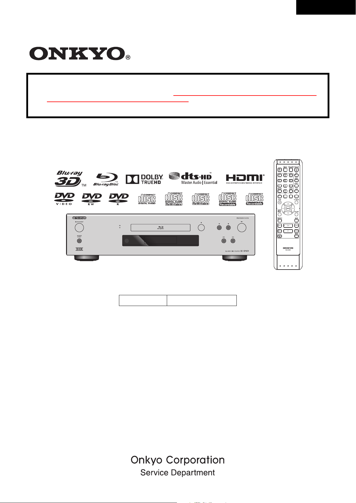
SERVICE MANUAL
RC-819DV
BD-SP809M2
Ref. No. 4482
072014
They are 2 types to this model (Model No. BD-SP809(B)/(S)), in which a different type of Boards and the
color of BARCODE LABEL are used.
This service manual is for models that ends with
and
"Blue" BARCODE LABEL is adhered on the rear panel
Before servicing, make sure to confirm these differences from the other same number of models, due
to the 2 types of Boards are not compatible.
"M2" at the end of the Current Version of the Firmware
of the unit.
BLU-RAY DISC PLAYER
MODEL
BD-SP809(B)/(S)
Black/Silver model
B/S CUP2BP 110-240V AC, 50/60Hz
Page 2

TABLE OF CONTENTS
Precautions on 3D video images
This unit supports Blu-ray 3D. When servicing problems related to 3D image output, the following
equipments are needed.
- 3D capable TV
- 3D compatible HDMI cable
- 3D glasses
- Blu-ray 3D disc
Manufactured under license from Dolby Laboratories.
Dolby and the double-D symbol are trademarks of Dolby Laboratories.
Specifications . . . . . . . . . . . . . . . . . . . . . . . . . . . . . . . . . . . . . . . . . . . . . . . . . . . . . . . . . . . . . . . . . . . . . . . . . . 1-1-1
Laser Beam Safety Precautions . . . . . . . . . . . . . . . . . . . . . . . . . . . . . . . . . . . . . . . . . . . . . . . . . . . . . . . . . . . . 1-2-1
Important Safety Precautions . . . . . . . . . . . . . . . . . . . . . . . . . . . . . . . . . . . . . . . . . . . . . . . . . . . . . . . . . . . . . . 1-3-1
Standard Notes for Servicing . . . . . . . . . . . . . . . . . . . . . . . . . . . . . . . . . . . . . . . . . . . . . . . . . . . . . . . . . . . . . . 1-4-1
Cabinet Disassembly Instructions . . . . . . . . . . . . . . . . . . . . . . . . . . . . . . . . . . . . . . . . . . . . . . . . . . . . . . . . . . . 1-5-1
How to Initialize the BLU-RAY Disc Player . . . . . . . . . . . . . . . . . . . . . . . . . . . . . . . . . . . . . . . . . . . . . . . . . . . . 1-6-1
Firmware Renewal Mode . . . . . . . . . . . . . . . . . . . . . . . . . . . . . . . . . . . . . . . . . . . . . . . . . . . . . . . . . . . . . . . . . 1-7-1
Adjustment Instructions for BD Main CBA or BD Mechanism Assembly Replacement . . . . . . . . . . . . . . . . . . 1-8-1
Error Message . . . . . . . . . . . . . . . . . . . . . . . . . . . . . . . . . . . . . . . . . . . . . . . . . . . . . . . . . . . . . . . . . . . . . . . . . 1-9-1
Block Diagrams . . . . . . . . . . . . . . . . . . . . . . . . . . . . . . . . . . . . . . . . . . . . . . . . . . . . . . . . . . . . . . . . . . . . . . . . 1-10-1
Schematic Diagrams / CBA and Test Points . . . . . . . . . . . . . . . . . . . . . . . . . . . . . . . . . . . . . . . . . . . . . . . . . . 1-11-1
Exploded View . . . . . . . . . . . . . . . . . . . . . . . . . . . . . . . . . . . . . . . . . . . . . . . . . . . . . . . . . . . . . . . . . . . . . . . . 1-12-1
Packing View. . . . . . . . . . . . . . . . . . . . . . . . . . . . . . . . . . . . . . . . . . . . . . . . . . . . . . . . . . . . . . . . . . . . . . . . . . 1-12-2
Mechanical Parts List . . . . . . . . . . . . . . . . . . . . . . . . . . . . . . . . . . . . . . . . . . . . . . . . . . . . . . . . . . . . . . . . . . . 1-13-1
Electrical Parts List . . . . . . . . . . . . . . . . . . . . . . . . . . . . . . . . . . . . . . . . . . . . . . . . . . . . . . . . . . . . . . . . . . . . . 1-14-1
Page 3

SPECIFICATIONS
General
Signal system NTSC / PAL Colour
Power requirements AC110-240 V, 50/60 Hz
Power consumption 21 W, standby: 0.3 W, standby(Power On Control): 3.5 W
Dimensions
(width x height x depth)
Weight 4.6 kg
Operating temperature 5 °C to 40 °C
Operating humidity Less than 80 % (no condensation)
BD Linear Audio 4 Hz–88 kHz (192 kHz)
DVD Linear Audio 4 Hz–44 kHz (96 kHz), 4 Hz–22 kHz (48 kHz)
Audio CD 4 Hz–20 kHz (44.1 kHz)
Signal to Noise Ratio 100 dB
Audio Dynamic Range 98 dB
THD (Total Harmonic Distortion)
USB input
TYPE A
Audio output (Analogue)
RCA jack x 2 L/R: 2 Vrms (output impedance:
Video output
RCA jack x 1 1Vp-p (75
Component video output
RCA jack x 3
Audio output (Digital)
RCA jack x 1
Optical jack x 1
HDMI output
HDMI jack x 2 Video: 480i/576i, 480p/576p, 720p, 1080i, 1080p, 1080p24 / Audio
ETHERNET terminal 10BASE-T/100BASE-TX
435 x 104 x 315 mm
Audio
0.005 % (1 kHz)
Terminals
USB 2.0
Bus power current: MAX. 500 mA
ƙ)
Y: 1 Vp-p (75 ƙ)
PB: 700 mVp-p (75 ƙ)
PR: 700 mVp-p (75 ƙ)
500 mVp-p (75 ƙ)
Digital connector
less than 1 kƙ
)
D Note
• The specifications and design of this product are subject to change without notice.
1-1-1 ECEB0SP
Page 4
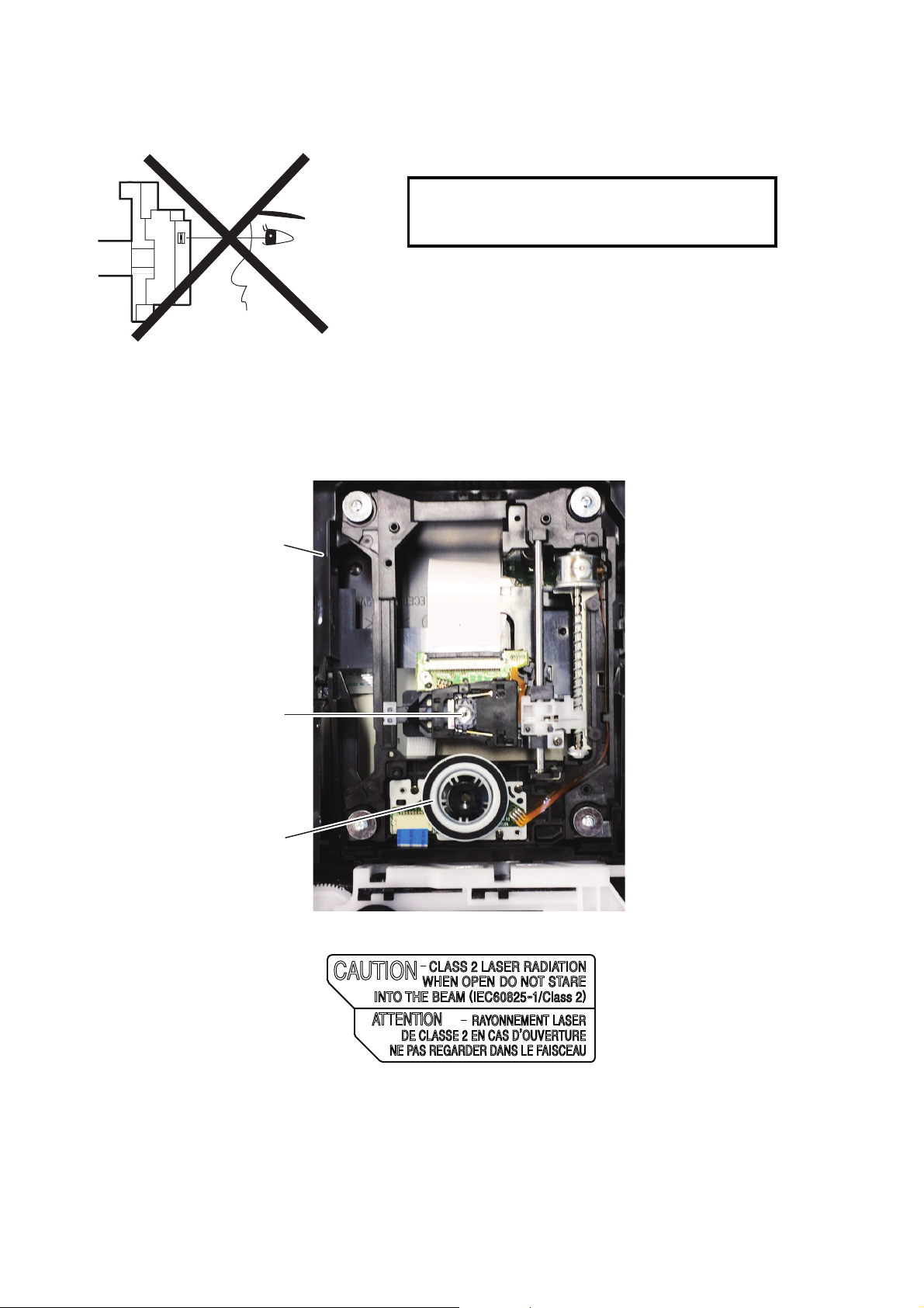
LASER BEAM SAFETY PRECAUTIONS
Do not look directly at the laser beam coming
from the pickup or allow it to strike against your
skin.
Drive Mechanism Assembly
Laser Beam Radiation
/Laser Pickup
Turntable
This BD player uses a pickup that emits a laser beam.
The laser beam is emitted from the location shown in the figure. When checking the laser diode, be sure to keep
your eyes at least 30 cm away from the pickup lens when the diode is turned on. Do not look directly at the laser
beam.
CAUTION: Use of controls and adjustments, or doing procedures other than those specified herein, may result in
hazardous radiation exposure.
Location: Inside Top of BD mechanism.
1-2-1 B2PLBSP
Page 5

IMPORTANT SAFETY PRECAUTIONS
Product Safety Notice
Some electrical and mechanical parts have special
safety-related characteristics which are often not
evident from visual inspection, nor can the protection
they give necessarily be obtained by replacing them
with components rated for higher voltage, wattage,
etc. Parts that have special safety characteristics are
identified by a ! on schematics and in parts lists. Use
of a substitute replacement that does not have the
same safety characteristics as the recommended
replacement part might create shock, fire, and/or other
hazards. The Product’s Safety is under review
continuously and new instructions are issued
whenever appropriate. Prior to shipment from the
factory, our products are carefully inspected to confirm
with the recognized product safety and electrical
codes of the countries in which they are to be sold.
However, in order to maintain such compliance, it is
equally important to implement the following
precautions when a set is being serviced.
Precautions during Servicing
A. Parts identified by the ! symbol are critical for
safety. Replace only with part number specified.
B. In addition to safety, other parts and assemblies
are specified for conformance with regulations
applying to spurious radiation. These must also be
replaced only with specified replacements.
Examples: RF converters, RF cables, noise
blocking capacitors, and noise blocking filters, etc.
C. Use specified internal wiring. Note especially:
1) Wires covered with PVC tubing
2) Double insulated wires
3) High voltage leads
D. Use specified insulating materials for hazardous
live parts. Note especially:
1) Insulation tape
2) PVC tubing
3) Spacers
4) Insulators for transistors
E. When replacing AC primary side components
(transformers, power cord, etc.), wrap ends of
wires securely about the terminals before
soldering.
F. Observe that the wires do not contact heat
producing parts (heatsinks, oxide metal film
resistors, fusible resistors, etc.).
G. Check that replaced wires do not contact sharp
edges or pointed parts.
H. When a power cord has been replaced, check that
5~6 kg of force in any direction will not loosen it.
I. Also check areas surrounding repaired locations.
J. Be careful that foreign objects (screws, solder
droplets, etc.) do not remain inside the set.
K. When connecting or disconnecting the internal
connectors, first, disconnect the AC plug from the
AC outlet.
L. When reassembling, be sure to use the original
screws or specified screws listed in the parts list.
M. This unit is classified as a CLASS 1 LASER
PRODUCT.
1-3-1 BDP_ISP
Page 6
Safety Check after Servicing
Table 2: Leakage current ratings for selected areas
Note: This table is unofficial and for reference only. Be sure to confirm the precise values.
AC Line Voltage Load Z Leakage Current (i)
One side of power cord plug
prongs (B) to:
230 V
2kRES.
Connected in
parallel
i0.7mA AC Peak
i2mA DC
RF or
Antenna terminals
50k RES.
Connected in
parallel
i0.7mA AC Peak
i2mA DC
A/V Input, Output
Examine the area surrounding the repaired location for
damage or deterioration. Observe that screws, parts,
and wires have been returned to their original positions.
Afterwards, do the following tests and confirm the
specified values to verify compliance with safety
standards.
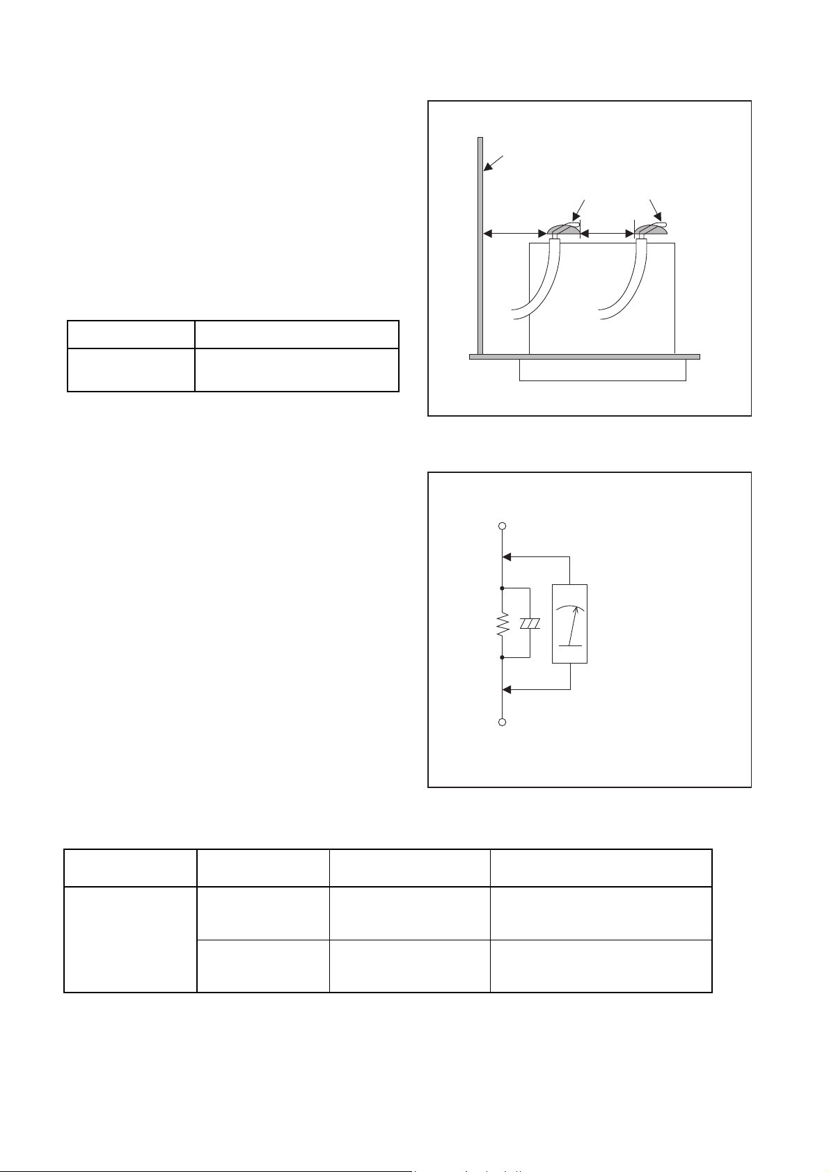
1. Clearance Distance
When replacing primary circuit components, confirm
specified clearance distance (d) and (d’) between
soldered terminals, and between terminals and
surrounding metallic parts. (See Fig. 1)
Table 1 : Ratings for selected area
AC Line Voltage Clearance Distance (d), (d’)
Chassis or Secondary Conductor
Primary Circuit
d' d
230 V
Note: This table is unofficial and for reference only.
Be sure to confirm the precise values.
3.2 mm(d)
6.0 mm(d’)
2. Leakage Current Test
Confirm the specified (or lower) leakage current
between B (earth ground, power cord plug prongs) and
externally exposed accessible parts (RF terminals,
antenna terminals, video and audio input and output
terminals, microphone jacks, earphone jacks, etc.) is
lower than or equal to the specified value in the table
below.
Measuring Method (Power ON) :
Insert load Z between B (earth ground, power cord plug
prongs) and exposed accessible parts. Use an AC
voltmeter to measure across the terminals of load Z.
See Fig. 2 and the following table.
Exposed Accessible Part
Z
One side of
B
Power Cord Plug Prongs
Fig. 1
AC Voltmeter
(High Impedance)
1-3-2 BDP_ISP
Fig. 2
Page 7
STANDARD NOTES FOR SERVICING
Top View
Out
In
Bottom View
Input
5
10
Pin 1
Pin 1
FFC Cable
Connector
CBA
* Be careful to avoid a short circuit.
Fig. S-1-1
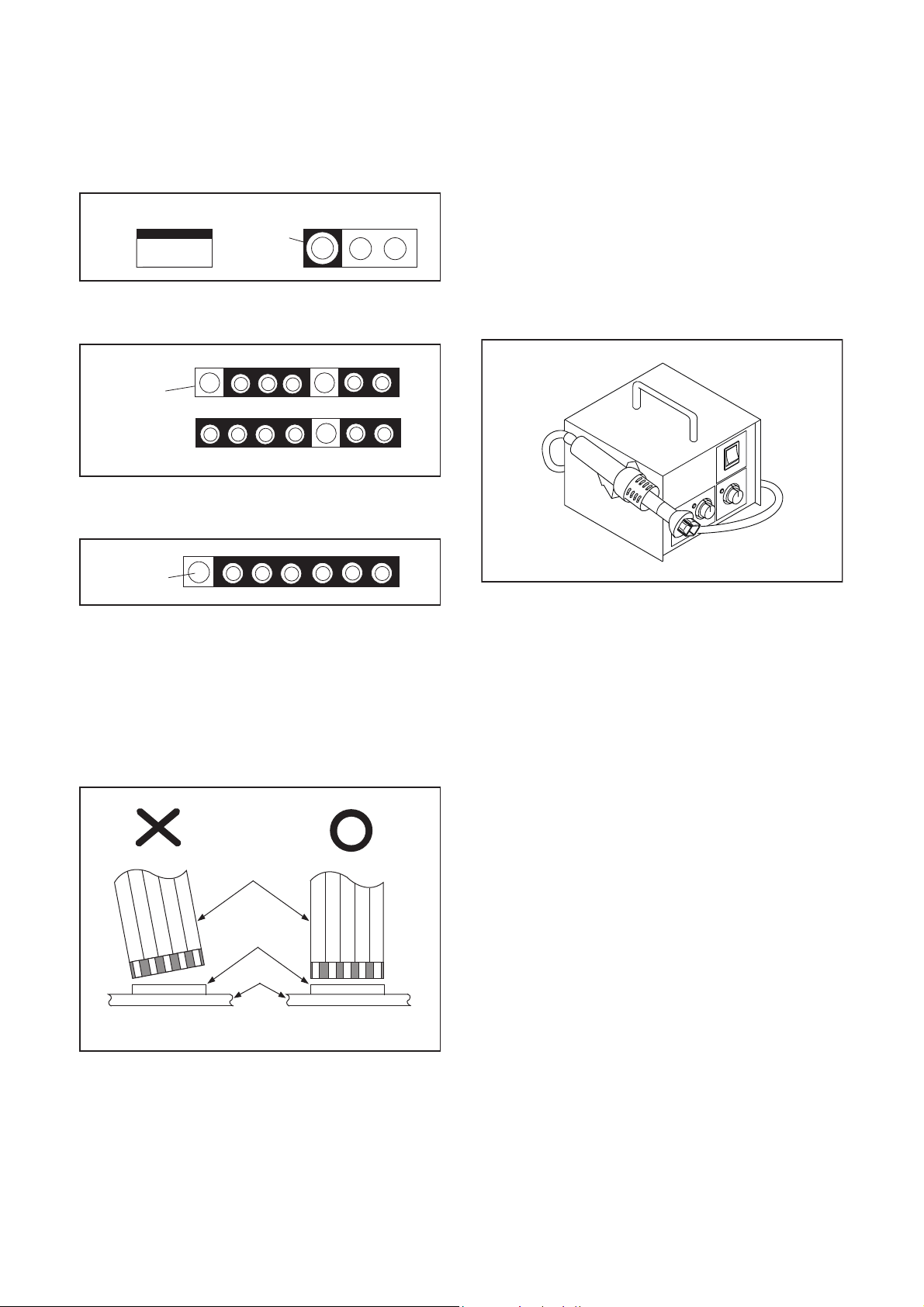
Circuit Board Indications
1. The output pin of the 3 pin Regulator ICs is
indicated as shown.
2. For other ICs, pin 1 and every fifth pin are
indicated as shown.
3. The 1st pin of every male connector is indicated as
shown.
Pb (Lead) Free Solder
When soldering, be sure to use the Pb free solder.
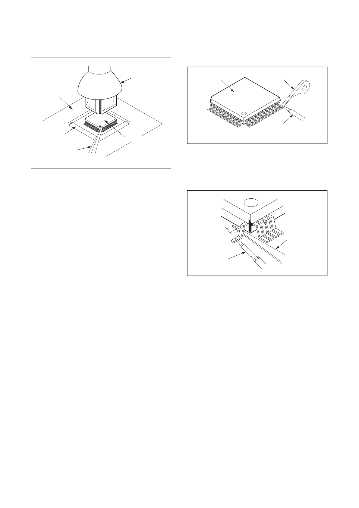
How to Remove / Install Flat Pack-IC
1. Removal
With Hot-Air Flat Pack-IC Desoldering Machine:
1. Prepare the hot-air flat pack-IC desoldering
machine, then apply hot air to the Flat Pack-IC
(about 5 to 6 seconds). (Fig. S-1-1)
Instructions for Connectors
1. When you connect or disconnect the FFC (Flexible
Foil Connector) cable, be sure to first disconnect
the AC cord.
2. FFC (Flexible Foil Connector) cable should be
inserted parallel into the connector, not at an
angle.
2. Remove the flat pack-IC with tweezers while
applying the hot air.
3. Bottom of the flat pack-IC is fixed with glue to the
CBA; when removing entire flat pack-IC, first apply
soldering iron to center of the flat pack-IC and heat
up. Then remove (glue will be melted). (Fig. S-1-6)
4. Release the flat pack-IC from the CBA using
tweezers. (Fig. S-1-6)
CAUTION:
1. The Flat Pack-IC shape may differ by models. Use
an appropriate hot-air flat pack-IC desoldering
machine, whose shape matches that of the Flat
Pack-IC.
2. Do not supply hot air to the chip parts around the
flat pack-IC for over 6 seconds because damage
to the chip parts may occur. Put masking tape
around the flat pack-IC to protect other parts from
damage. (Fig. S-1-2)
1-4-1 BDP_SN
Page 8
3. The flat pack-IC on the CBA is affixed with glue, so
Hot-air
Flat Pack-IC
Desoldering
Machine
CBA
Flat Pack-IC
Tweezers
Masking
Tape
Fig. S-1-2
Fine Tip
Soldering Iron
Sharp
Pin
Fig. S-1-4
be careful not to break or damage the foil of each
pin or the solder lands under the IC when
removing it.
With Soldering Iron:
1. Using desoldering braid, remove the solder from
all pins of the flat pack-IC. When you use solder
flux which is applied to all pins of the flat pack-IC,
you can remove it easily. (Fig. S-1-3)
Flat Pack-IC
Desoldering Braid
Soldering Iron
Fig. S-1-3
2. Lift each lead of the flat pack-IC upward one by
one, using a sharp pin or wire to which solder will
not adhere (iron wire). When heating the pins, use
a fine tip soldering iron or a hot air desoldering
machine. (Fig. S-1-4)
3. Bottom of the flat pack-IC is fixed with glue to the
CBA; when removing entire flat pack-IC, first apply
soldering iron to center of the flat pack-IC and heat
up. Then remove (glue will be melted). (Fig. S-1-6)
4. Release the flat pack-IC from the CBA using
tweezers. (Fig. S-1-6)
1-4-2 BDP_SN
Page 9
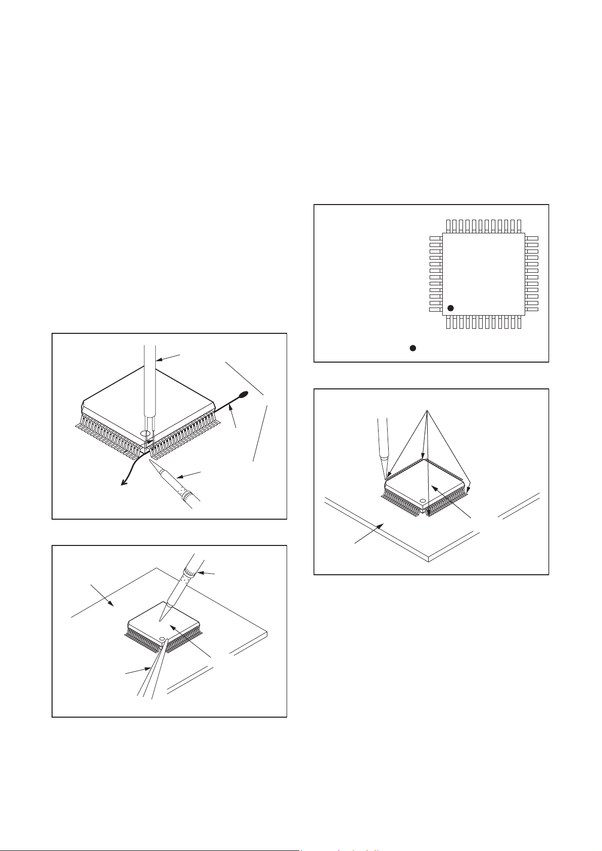
With Iron Wire:
To Solid
Mounting Point
Soldering Iron
Iron Wire
or
Hot Air Blower
Fig. S-1-5
Fine Tip
Soldering Iron
CBA
Flat Pack-IC
Tweezers
Fig. S-1-6
Example :
Pin 1 of the Flat Pack-IC
is indicated by a " " mark.
Fig. S-1-7
1. Using desoldering braid, remove the solder from
all pins of the flat pack-IC. When you use solder
flux which is applied to all pins of the flat pack-IC,
you can remove it easily. (Fig. S-1-3)
2. Affix the wire to a workbench or solid mounting
point, as shown in Fig. S-1-5.
3. While heating the pins using a fine tip soldering
iron or hot air blower, pull up the wire as the solder
melts so as to lift the IC leads from the CBA
contact pads as shown in Fig. S-1-5.
4. Bottom of the flat pack-IC is fixed with glue to the
CBA; when removing entire flat pack-IC, first apply
soldering iron to center of the flat pack-IC and heat
up. Then remove (glue will be melted). (Fig. S-1-6)
5. Release the flat pack-IC from the CBA using
tweezers. (Fig. S-1-6)
Note: When using a soldering iron, care must be
taken to ensure that the flat pack-IC is not
being held by glue. When the flat pack-IC is
removed from the CBA, handle it gently
because it may be damaged if force is applied.
2. Installation
1. Using desoldering braid, remove the solder from
the foil of each pin of the flat pack-IC on the CBA
so you can install a replacement flat pack-IC more
easily.
2. The “ I ” mark on the flat pack-IC indicates pin 1.
(See Fig. S-1-7.) Be sure this mark matches the
pin 1 on the PCB when positioning for installation.
Then presolder the four corners of the flat pack-IC.
(See Fig. S-1-8.)
3. Solder all pins of the flat pack-IC. Be sure that
none of the pins have solder bridges.
Presolder
Flat Pack-IC
CBA
Fig. S-1-8
1-4-3 BDP_SN
Page 10
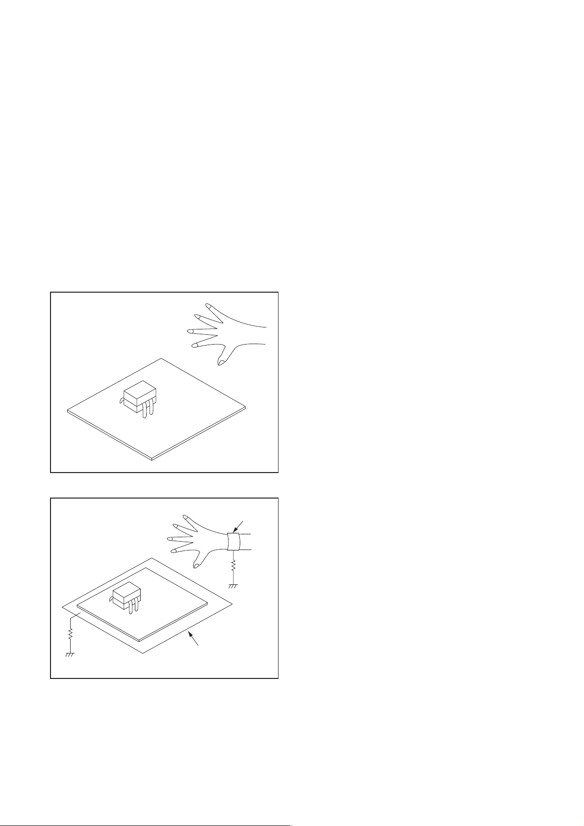
Instructions for Handling Semi-
<Incorrect>
CBA
Grounding Band
Conductive Sheet or
Copper Plate
1MΩ
1MΩ
<Correct>
CBA
conductors
Electrostatic breakdown of the semi-conductors may
occur due to a potential difference caused by
electrostatic charge during unpacking or repair work.
1. Ground for Human Body
Be sure to wear a grounding band (1 M) that is
properly grounded to remove any static electricity that
may be charged on the body.
2. Ground for Workbench
Be sure to place a conductive sheet or copper plate
with proper grounding (1 M) on the workbench or
other surface, where the semi-conductors are to be
placed. Because the static electricity charge on
clothing will not escape through the body grounding
band, be careful to avoid contacting semi-conductors
with your clothing.
1-4-4 BDP_SN
Page 11
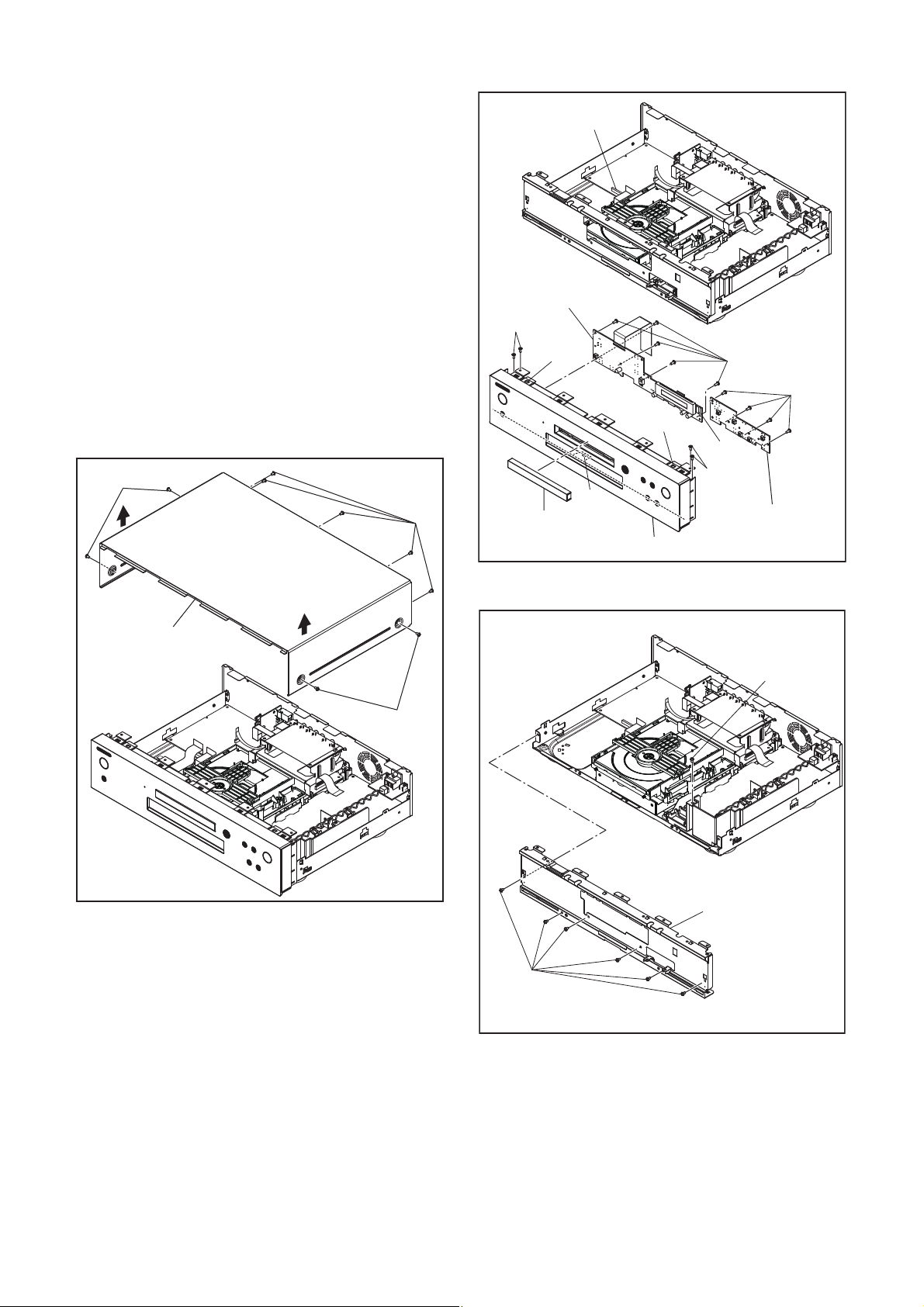
CABINET DISASSEMBLY INSTRUCTIONS
[3] Front
Assembly
[1] Top Cover
[2] Tray
Assembly
[9] Rear Panel
[11] Video CBA
[12] AV PCB
Bracket
[14] BD Main
CBA Unit
[18] Loader
Bracket
[8] RS232C
CBA
[7] Inlet CBA
[6] Front Bracket
[15] BD Mechanism
Assembly
[13] BD Main CBA
& BD Mechanism
Assembly
[17] Power
Holder
[16] Power
Supply CBA
[10] Audio CBA
[4] Front-A CBA
[5] Front-B CBA
1. Disassembly Flowchart
This flowchart indicates the disassembly steps to gain
access to items to be serviced. When reassembling,
follow the steps in reverse order. Bend, route, and
dress the cables as they were originally.
ID/
Loc.
Part
No.
[10] Audio CBA D5
Fig.
No.
4(S-12), CN2001,
CN2201
Removal
Note
[11] Video CBA D6 4(S-13), CN6901 ---
AV PCB
[12]
Bracket
D6 4(S-14) ---
BD Main
[13]
CBA & BD
Mechanism
2(S-15), 4(S-16),
D7
CN6101
Assembly
[14]
[15]
BD Main
CBA Unit
BD
Mechanism
Assembly
CN7001, CN7002,
D8
CN7003, Hook
4(S-17),
D8
Loader Holder
Power
[16]
Supply
D9 3(S-18), 2(S-19) ---
CBA
Power
[17]
[18]
(1)
Holder
Loader
Bracket
(2)
D9 3(S-20) ---
D9 6(S-21) ---
(3)
(4)
---
---
4
4
(5)
2. Disassembly Method
ID/
Loc.
No.
[1] Top Cover D1 9(S-1) ---
[2]
[3]
[4]
[5]
[6]
[7]
[8]
[9] Rear Panel D4
Part
Tr ay
Assembly
Front
Assembly
Front-A
CBA
Front-B
CBA
Front
Bracket
Inlet CBA
RS232C
CBA
Fig.
No.
D2 --------------- 1
D2
D2 CN3001 ---
D2 --------------- ---
D3 7(S-4) ---
D4 (S-5), 2(S-6), CN1002 5
D4 (S-7), 2(S-8), CN5501 ---
Removal
2(L-1), (L-2), 4(S-2),
9(S-3), CN2002
8(S-9), 2(S-10),
5(S-11)
Note
2
3
Note:
(1) Identification (location) No. of parts in the figures
(2) Name of the part
(3) Figure Number for reference
(4) Identification of parts to be removed, unhooked,
unlocked, released, unplugged, unclamped, or
desoldered.
P = Spring, L = Locking Tab, S = Screw,
CN = Connector
e.g. 2(S-2) = two Screws of (S-2),
2(L-2) = two Locking Tabs of (L-2)
(5) Refer to “Reference Notes.”
1-5-1 ECEB0DC
Page 12
Reference Notes
1. How to remove Tray Assembly
1) Press the [A] button to open the tray.
2) Remove the Tray Assembly.
3) Press the [A] button to close the tray.
2. CAUTION 1: Locking Tabs (L-1) and (L-2) are
fragile. Be careful not to break them.
3. When reassembling, be sure to use the original
screws or specified screws listed in the parts
list.
4. When replacing the BD Mechanism Assembly
or BD Main CBA Unit, refer to “ADJUSTMENT
INSTRUCTIONS FOR BD MAIN CBA OR BD
MECHANISM ASSEMBLY REPLACEMENT.”
5. Make sure there is no gap left between the
Rear Panel and AC Inlet Terminal when
assembling Inlet CBA.
(S-1)
(S-1)
CN2002
[4] Front-A CBA
(S-2)
(L-1)
(L-2)
[2] Tray
Assembly
(S-3)
(L-1)
CN3001
(S-2)
[5] Front-B CBA
[3] Front Assembly
(S-3)
Fig. D2
[1] Top Cover
(S-4)
(S-1)
Fig. D1
[6] Front Bracket
(S-4)
Fig. D3
1-5-2 ECEB0DC
Page 13
*See Reference Note 3.
[9] *Rear Panel
(S-9)
(S-7)
(S-8)
(S-11)
(S-11)
[8] RS232C
CBA
CN5501
(S-10)
CN1002
[7] Inlet CBA
CAUTION: When assembling the Inlet CBA
(Rear View)
(S-9)
(S-11)
(S-5)
(S-6)
[11] Video CBA
(S-14)
[12] AV PCB
Bracket
CN6901
[13] BD Main CBA &
BD Mechanism
Assembly
(S-13)
(S-14)
Fig. D6
(S-16)
Make sure there is no gap left between
the Rear Panel and AC Inlet Terminal.
(S-12)
[10] Audio CBA
CN2201
CN2001
(S-15)
Fig. D4
CN6101
Fig. D7
Fig. D5
1-5-3 ECEB0DC
Page 14
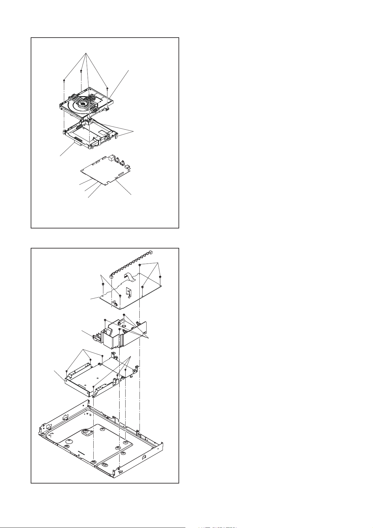
Loader Holder
CN7003
CN7001
CN7002
(S-17)
[15] *BD Mechanism
Assembly
Hook
[14] *BD Main CBA Unit
* See Reference Note 4.
(S-19)
[16] Power Supply
CBA
[17] Power Holder
(S-21)
[18] Loader
Bracket
Fig. D8
(S-18)
(S-20)
(S-21)
Fig. D9
1-5-4 ECEB0DC
Page 15
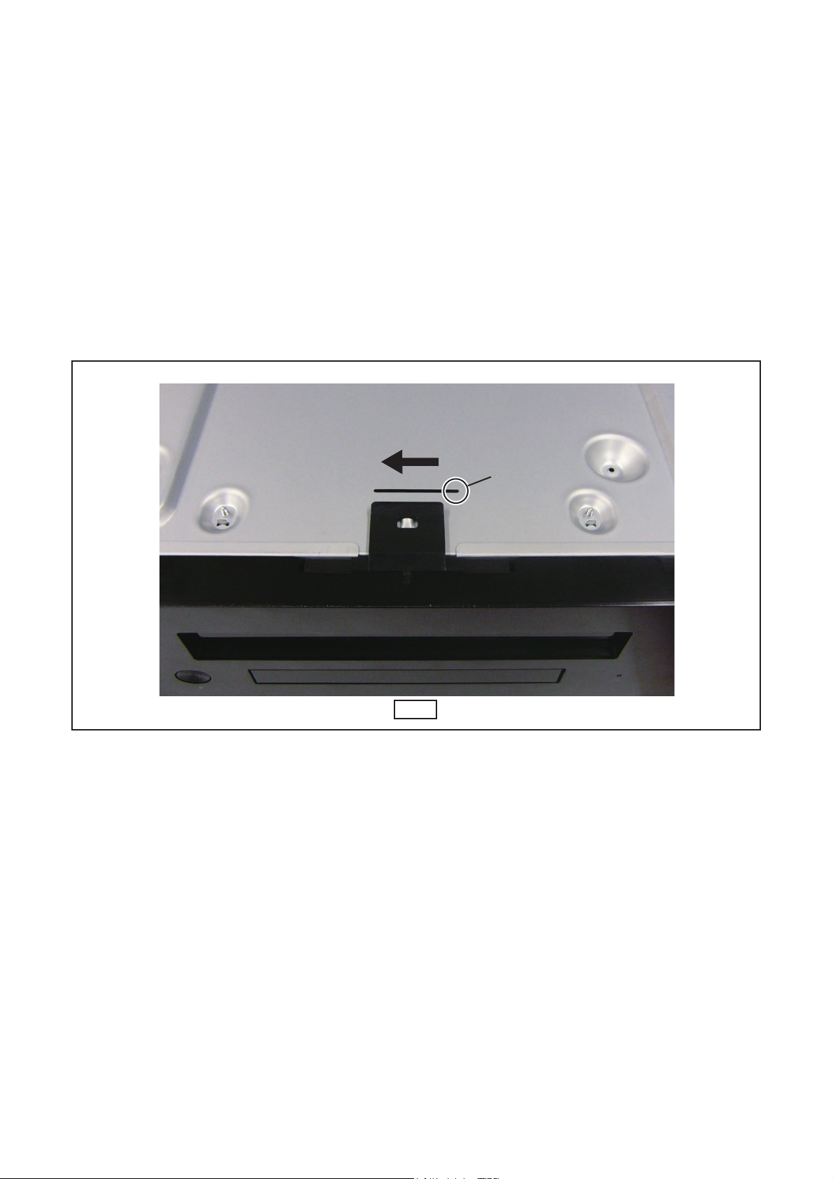
3. How to Eject a Disc
When a disc cannot be removed due to malfunction or when an unplayable disc is inserted, follow the
procedure below to remove the disc.
Procedure A
1. Unplug the AC power cord and then plug it in.
2. Turn the power on by pressing the [A] button and the disc tray will open automatically.
Procedure B
1. Unplug the AC power cord.
2. Turn the unit over.
3. Insert a straight shaft of 1.5mm in diameter or less into the location marked A below. (Refer to the
illustration below.)
4. Move the shaft slowly in the direction of the arrow. (Refer to the illustration below.)
5. Pull the tray slowly manually.
A
Front
1-5-5 ECEB0DC
Page 16

HOW TO INITIALIZE THE BLU-RAY DISC PLAYER
To put the program back at the factory-default,
initialize the BD player as the following procedure.
Note:
• By initializing, network is reset to disconnected state.
1. Turn the power on.
2. Remove the disc on the tray and close the tray.
3. Press [ ] (skip up), [1], [2], and [3] buttons on
the remote control unit in this order.
Fig. a appears on the screen. All VFD lights.
"*" differ depending on the models.
Version Display
F/W Name
Version
Region
Pickup
Default Setting : --
Default Setting : STOP End : STANDBY-ON
VFD/LED Check : OK
: *******
: *.**.**
: *-*
: **
Fig. a
4. Press [ C ] button on the remote control unit.
Fig. b appears on the screen and Fig. c appears
on the VFD.
"*" differ depending on the models.
Version Display
F/W Name
Version
Region
Pickup
Default Setting : SUCCESS
Default Setting : STOP End : STANDBY-ON
VFD/LED Check : OK
: *******
: *.**.**
: *-*
: **
Fig. b
Fig. c
5. After initializing, the power will turn off
automatically.
1-6-1 E5XF1INT
Page 17
FIRMWARE RENEWAL MODE
"*" differ depending on the models.
F/W Version Mode
Please select software update mode.
Disc
USB
SD Card
F/W Name : ******* Ver *.**.**
The available software update mode will
differ depending on the model type.
"*" differ depending on the models.
F/W Version Mode
Loading Disc...
F/W Name : ******* Ver *.**.**
(*1)
Note: The file extension of the available firmware is
“b40”.
1. Turn the power on and remove the disc on the tray
and close the tray.
2. Press [ ] (skip up), [6], [5], and [4] buttons on
the remote control unit in that order.
Fig. a appears on the screen.
Fig. a Version Up Mode Screen (Example)
3. Select “Disc” or “USB” and press [ENTER] button
on the remote control unit. The tray will open
automatically, if “Disc” is selected.
4. Insert the disc or USB Flash Drive for version up.
5. The BD player enters the F/W version up mode
automatically. Fig. b will appear on the screen.
Make sure to insert the proper F/W for the state of
this model.
The appearance shown in (*1) of Fig. b is
described as follows:
No. Appearance State
1 Loading Disc Loading the disc
2 Reading...
Sending files into the
memory.
Writing new version data,
3See FLD.
the progress will be displayed
as shown in Fig. d.
"*" differ depending on the models.
F/W Version Mode
1. ALL
Version : *.**.**
CHECKSUM : ****
See FLD.
The unit will automatically turn off when update is completed,
and automatically turns back on.
F/W Name : ******* Ver *.**.**
***************.b40
Fig. c Version Up Mode
Fig. d VFD in Version Up Mode
6. After the update, Fig. e will appear on the VFD and
the power will turn off automatically.
Fig. b Programming Mode Screen (Example)
Fig. e
VFD upon Finishing the Programming Mode (Example)
7. The power turns on automatically. If disc mode
was selected, the tray will open automatically.
Remove the disc or USB Flash Drive from the unit.
Note: All the settings will be put back to factory-
default.
The following USB Flash Drive can be used for
software update. Make sure to use a device that has
enough space.
• USB Flash Drive (FAT16/FAT32 file system)
• Choose “USB” at Fig. a. when using a SD Card that
is connected to a Card Reader. Otherwise, the unit
will not be updated if “SD Card” is selected.
1-7-1 BD-SP809M2FW
Page 18

How to Verify the Firmware Version
Product Info
OK
Current Version : X.XX.XXM2
If you wish to check latest update or
other product information, please check
our Website.
"X" differ depending on the models.
www.onkyo.com
1. Turn the power on.
2. Press [Home] button on the remote control unit.
3. Select “Settings” on the home menu screen and
press [ENTER] button.
4. Select “Others” then press [ENTER] button.
5. Select “Product Info” then press [ENTER] button.
Refer to Fig. f below.
Fig. f
Note: There are two types to this model (Model
No.BD-SP809(B)/(S)), in which a different type
of Board is used.This service manual is for
models that ends with "M2" at the end of the
Current Version.
1-7-2 BD-SP809M2FW
Page 19

ADJUSTMENT INSTRUCTIONS FOR BD MAIN CBA OR
BD MECHANISM ASSEMBLY REPLACEMENT
When replacing either BD Main CBA or BD Mechanism Assembly, the unique OPU DATA of the BD Mechanism
needs to be written into the BD Main CBA. Follow the procedure below for OPU DATA write operation.
Equipments:
• PC (OS: Windows 7 strongly recommended)
• Barcode reader
• LAN cable (Cross Type)
• Short-circuit clip
• Specialized application (OpuDataWriter)
1. Preparation Of Work Environment
1-1.
For the OPU DATA write operation, refer to the connection diagram and connect each device as shown below.
Connection Diagram
Unit (Rear View)
PC
LAN cable
(Cross Type)
Barcode Reader
(To USB Port)
2. PC Setup
2-1. Change the PC's IP address to "192.168.0.1".
2-2. Install the VB6 Runtime.
If “mswinsck.ocx” exists under “C:\windows\system32\”, you do not need to install this.
2-3. Remove the Top Cover. Refer to the “CABINET DISASSEMBLY INSTRUCTIONS” section on page 1-5-1.
2-4. Connect the short-circuit clip as the illustration below.
1-8-1 B4.8P_AIR
Page 20

3. Application Setup
Status Display
Cursor position
Status Display
3-1. Save the application folder (OpuDataWriter) directly under the C: drive.
3-2. Create a shortcut for [OpuDataWriter.exe] which is located inside the folder on the desktop.
4. OPU DATA WRITE
4-1. Connect the unit’s AC power cord. Wait for about 30 seconds until the unit is in standby mode.
4-2. Double click on the [OpuDataWriter.exe] shortcut on the desktop to start the application.
4-3. Application start screen appears.
Check that [Please input OPU DATA] message is displayed in the Status Display.
Set the cursor position at the blank box next to the [OPU DATA].
4-4. Using the Barcode reader, scan the QR code attached to the BD Mechanism Assembly.
4-5. Check that [FE CONNECTION CHECK] message appears on the Status Display then turn the unit power on.
FE CONNECTION CHECK
If error occurs:
If an error occurs, the screen changes to a red display. In such case, close the window and then unplug the
unit AC power cord. Check if each device is properly connected then repeat from step 1.
1-8-2 B4.8P_AIR
Page 21

4-6. Data write begins. While writing data, the Status Display message will change.
Status Display
SEND LD PAR
[OK]
4-7. [OK] appears in the Status Display if data write has been completed successfully.
If error occurs:
• If an error occurs, the screen changes to a red display. In such case, close the window and then unplug the
unit AC power cord. Check if each device is properly connected then repeat from step 1.
• If an error other than connection error occurs for more than 3 times, the BD MAIN CBA or BD Mechanism
Assembly may be defected. Replace with a new one before performing the OPU DATA write.
[ERROR:1210] ComConnection TIME OUT.
4-8. After data write has been completed successfully, unplug the AC power cord.
4-9. Remove the LAN Cable.
1-8-3 B4.8P_AIR
Page 22

Error Code
Error Code Error Description
10 Start word error The first letter entered for [OPU DATA] does not match.
210 Start word error The first letter entered for [OPU DATA] does not match.
300 CheckSum NG
1010 Start word error The first letter entered for [OPU DATA] does not match.
2300 OPU Model Check NG The model type of OPU is not registered.
2310 Drive Parameter CheckSum NG Data checksum of acquired IOP data does not match.
3001
3002 LanConnectionChk Nop Error No response for NOP confirmation after LAN connection.
3003 LanConnectionChk Other Error Error occurred during LAN connection process.
3011 LanGenerationChk TIME OUT Generation check failed. (Timeout)
3012 LanGenerationChk Other Error Generation check failed. (Other error)
3021
3022
3141 LanB2LdParamSend TIME OUT LD Parameter data send process failed. (Timeout)
3142
3143
3161 LanB2IopSet ERROR0 IOP measure failed. (ERROR0)
3162 LanB2IopSet ERROR1 IOP measure failed. (ERROR1)
3163 LanB2IopSet TIME OUT IOP measure failed. (Timeout)
3164 LanB2IopSet ETC IOP measure failed. (ETC)
3165 LanB2IopSet ERROR0 Switching off LD process after IOP measure failed. (ERROR0)
3166 LanB2IopSet ERROR1 Switching off LD process after IOP measure failed. (ERROR1)
3167 LanB2IopSet TIME OUT Switching off LD process after IOP measure failed. (Timeout)
3168 LanB2IopSet ETC Switching off LD process after IOP measure failed. (ETC)
3169 LanB2IopSet TIME OUT
3170 LanB2IopSet Rcvdata Error
3171 LanB2IopSet Rcvdata Error
3172 CD Iop LIMIT NG Exceeds the CD lop limit value.
3174 DVD Iop LIMIT NG Exceeds the DVD lop limit value.
3176 BD Iop LIMIT NG Exceeds the BD lop limit value.
3178 LanB2IopSet Other Error
3181
3182
3183
3184
3185
LanConnectionChk Connection
Error
LanB2DDDDataSend TIME
OUT
LanB2DDDDataSend Other
Error
LanB2LdParamSend Rcvdata
Error
LanB2LdParamSend Other
Error
LanB2LdParamVerify TIME
OUT
LanB2LdParamVerify Rcvdata
Error
LanB2LdParamVerify Rcvdata
Error
LanB2LdParamVerify Rcvdata
Error
LanB2LdParamVerify Other
Error
The checksum of the entered OPU DATA(QR code) does not
match.
Cannot connect to LAN.
Error occurred while sending OPU data. (Timeout)
Error occurred while sending OPU data. (Other error)
LD Parameter data send process failed. (Return value is invalid)
LD Parameter data send process failed. (Other error)
IOP measure sequence failed in the middle of the process.
(Timeout)
IOP measure sequence failed in the middle of the process.
(Return value is invalid)
IOP measure sequence failed in the middle of the process.
(Return value is invalid)
IOP measure sequence failed in the middle of the process.
(Other error)
Verify process failed. (Timeout)
Verify process failed. (Return value is invalid)
Verify process failed. (Return value is invalid)
Verify process failed. (Return value is invalid)
Verify process failed. (Other error)
1-8-4 B4.8P_AIR
Page 23

Error Code Error Description
Pre-operation OPU DATA text file
Year(2014)Month(06)
1406
3231
3232
3233 LanFactoryInfoSave Other Error Failed to read FactoryInfo data. (Other error)
3241 CreateFactoryInfo Other Error Failed to create FactoryInfo file.
LanFactoryInfoSave OPU SN
Error
LanFactoryInfoSave Fac Data
Error
Failed to read FactoryInfo data. There is a problem in reading
OPU SN.
Failed to read FactoryInfo data. There is a problem in reading
FACTORY data.
5. Saving The Pre-Operation OPU DATA
OPU DATA before performing the OPU DATA write is saved in a folder automatically.
5-1. When the OPU DATA write operation has been completed successfully, a folder named [FactoryInfo] is
created in the application folder (OpuDataWriter).
5-2. In the [FactoryInfo] folder, a folder is created monthly in which text file data are saved.
This text file is created with a file name of the OPU serial number and contains the pre-operation OPU DATA.
5-3. The text file is necessary for analyzing the defective BD Mechanism. Submit this text file with the defective
BD Mechanism as necessary to the appropriate managing Department.
1-8-5 B4.8P_AIR
Page 24

ERROR MESSAGE
Note: Only error messages for the unit’s corresponding media will appear.
Disc Error
Playback feature may not be available on this Disc.
Error Message
Disc Error
Loader Error
- - Please eject the disc. - -
Disc Error
- - Please eject the disc. - Playback feature may not be available on this Disc.
Loader Error
The unit stopped automatically due to loader error.
Please open the disc tray once and then close it.
Parental Lock Error
Region Error
The device connected for HDMI
connection does not support HDCP
USB Error
BD-Live Network Connecting Error
LAN Cable Not Connected
Cannot Acquire DHCP Server
Cannot Acquire IP Address
Parental Lock On
The current selected parental level prohibits playback.
Region Error
Playback is not authorized in your region.
Region code of this disc :
(There is no message.)
The following error will appear on the VFD.
Memory Device Error
- - Please check the Memory Device. - There is no playback file on the Memory Device or Device has incorrect/
no format.
BD-Live Setting Error
Network connection is interrupted. Please confirm “BD-Live Setting”.
The cable is not connected.
Please confirm the connection of the cable.
DHCP cannot be acquired.
Please confirm connection or set it with the manual operation.
Internet Protocol address is not set.
Please confirm the set content.
Already Existing IP Address
No Response From Default
Gateway
Cannot Connect To DNS Server
Cannot Connect To Server
Cannot Confirm Firmware Version
The equipment with same Internet Protocol address already exists.
Please set another Internet Protocol address.
There is no response from Default gateway.
Please confirm the address of Default gateway.
It is not possible to connect to the DNS server.
Please confirm the Internet connection or the DNS address setting.
It is not possible to connect to the server.
Please contact our support center.
It is not possible to confirm the software version.
Please contact our support center.
1-9-1 E5XF1ER
Page 25

Error Message
Firmware Update Error
(Update File Error)
Cannot Connect To Download
Server
USB Error
Error detected.
File may be corrupted.
Please download software again.
Error detected.
Please confirm whether it is USB device that corresponds to software
update.
It is not possible to connect to the server.
Please contact our support center.
Error in the USB Connection. USB operation has been stopped
automatically. Please remove the USB device and restart the unit.
1-9-2 E5XF1ER
Page 26

BLOCK DIAGRAMS
System Control Block Diagram
VFD
TO POWER SUPPLY
BLOCK DIAGRAM
PWSW4
TO VIDEO/AUDIO
BLOCK DIAGRAM
VIDEO-MUTE
19 20 21 22
FL3002
REMOTE
RS3002
CN2002 CN3002CN002 CN2001
SENSOR
345
FL-SDA
FL-SCL
315
456
6
FL-STB
FL-RESET
P-ON+5V
16KEY-1
REMOTE
12 12
16
3D
D3004
Q3004
POWER
SW3008
SW3009
SOURCE DIRECT
KEY-1
17 17
15 15
2 2
CN3101 CN3001
FRONT-A CBA
(MAIN MICRO CONTROLLER)
IC100
A13
PWSW4
CEC-IN
B12
A8
VIDEO-MUTE
CK27XI
CK27XO
A10
B10
XRST
E16
XFERST
F20
151413
FL-SDA
FL-SCL
141312
C9E9D9
FL-SCL
FL-SDA
XTRST
D16
12
FL-STB
FL-RESET
FL-STB
6
2
REMOTE
KEY-1
621 1
D8
B11
KEY-1
REMOTE
KEY-2 KEY-2
3D-LED 3D-LED
3 3
E8
E13
KEY-2
3D-LED
XRST-STM
F15
F14
B13
C13
FL-RESET
RS232C-TXD
RS232C-RXD
AUDIO CBA
KEY
SWITCH
FRONT-B CBA
CN551CN4002 CN4000CN5501
12131515
RS232C-RXD
RS232C-TXD
12
13
REMOTE
VIDEO CBA
3
4
11
RS232C-RXD
RS232C-TXD
REMOTE
3
4
BD MAIN CBA UNIT
JK801
HDMI-
CONNECTOR
Q801
(MAIN)
BUFFER
13
CEC
X251
27MHz
X'TAL
IC251
RESET
EV+11V
1-10-1
IC254
RESET
EV+3.3V
RS232C CBA
RS232C
IC5500
12
INTERFACE
13
3RXD
CN5500
RS232C-
CONNECTOR
11
RS232C
I/F
14
2TXD
PHOTO
IC5550
JK5550
Q5551,Q5552
COUPLER
REMOTE
-OUT
BUFFER
3
4
1
2
REMOTE
-IN
ECEB0BLS
Page 27

Digital Signal Process 1 Block Diagram
VIDEO SIGNAL AUDIO SIGNAL
MPX
/LPP
WOB
TO DIGITAL SIGNAL
PROCESS 2 BLOCK
DIAGRAM
(IC100)
STREAM
CONTROL
FE
DIGITAL
SIGNAL
PROCESS
RF
EQUALIZER
TRACKING-CONTROL
C19
FOCUS1-CONTROL
B19
COPY
PROTECT
AACS
FOCUS2-CONTROL
A19
BD+
CSS
CPRM
EXPA-CONTROL
D19
EXPB-CONTROL
E19
SLED1-CONTROL
SLED2-CONTROL
B17
A1737
LOAD-CONTROL
F19
TRAY-IN
B18
SPINDLE-CONTROL
C1719
SPINDLE-FG
B2022
BD MAIN CBA UNIT
(MAIN MICRO CONTROLLER/DIGITAL SIGNAL PROCESS)
IC100
MATRIX
E26, F25
D26, E25,
B26, C25,
*1: 32, 33, 36, 37
*2: 31, 34, 35, 38
CN701
A-D *1
E-H *2
C26, D25
RF(-) 27
RF(+) 28
LDD-SDATA 20
OEIC
(BDCD/DVD)
RF
GENERATOR
LDD-SDATA
LDD-SCLK
L22
G26
L23
G25
LDD-SCLK 19
27
TRACKING
ACTUATOR
IC701 (MOTOR DRIVE)
262524
CN701
TD 3
TR 4
DRIVE
FR1 5
LASER
FOCUS 1
ACTUATOR
DRIVE
23
FD1 6
FR2 1
DIODE
DRIVE
FOCUS 2
22
FD2 2
EXPA(+) 44
29
ACTUATOR
DRIVE
21
EXPA(-) 45
162815
COLLIMATE
LENS
MOTOR DRIVE
201918
EXPB(-) 43
EXPB(+) 42
SLED
MOTOR DRIVE
17
40
41
CN702
SLD2(-) 7
SLD2(+) 6
SLED
MOTOR
7
38
SPINDLE
MOTOR
7
CN702
U4
DRIVE
11
10
V3
W2
SPINDLE
MOTOR
6
COM 1
BD MECHANISM
ASSEMBLY
LOADING
MOTOR DRIVE
4
5
2
1
CN703
SLD1(-) 9
LOAD(-) 2
SLD1(+) 8
LOAD(+) 1
LOADING
MOTOR
IC702 (MOTOR DRIVE)
TRAY-IN 4
TRAY-IN
1-10-2
ECEB0BLD1
Page 28

Digital Signal Process 2 Block Diagram
DDC DATA
DDC CLOCK
TMDS DATA2-
TMDS DATA2+
TMDS DATA1-
TMDS DATA1+
TMDS DATA0-
TMDS DATA0+
TMDS CLOCK+
TO VIDEO/AUDIO
BLOCK DIAGRAM
HOT PLUG DETECT
HDMI-CONNECTOR
(MAIN)
JK801
191516
31649
7
10
TMDS CLOCK-
12
HOT PLUG DETECT
HDMI-CONNECTOR
(SUB)
JK401
191516
DDC DATA
DDC CLOCK
TMDS DATA2-
TMDS DATA2+
31649
TMDS DATA1-
TMDS DATA1+
TMDS DATA0-
TMDS DATA0+
7
TMDS CLOCK+
TMDS CLOCK-
10
12
TO VIDEO/AUDIO
BLOCK DIAGRAM
VIDEO
VIDEO SIGNAL AUDIO SIGNAL
VIDEO-Y(I/P)
VIDEO-Pb/Cb
T1
R2
VIDEO-Pr/Cr
IC803
IC801 (SCALER)
T2
U1
DDR2 SDRAM
(DDR2 SDRAM)
DDR2-DQ (0-15)
DDR2-A (0-12)
A4-A6,B5,
C5,C6,D5,
E2-E4,F3,
F4
DATA-Y(0-11)
E4, E5,
F4-F6,
G4-G6,
H4, H5,
J4, J5
(512Mbit)
A2,A3,B1,
B3,B4,C2,
DATA-C(0-11)
E2, E3,
F2, F3,
K15
C15
C4,D3,E1,
G2-G4
G1-G3,
H1-H3,
J2, J3
P15
P16
C14
HDMI
SIGNAL
PROCESS
/SCALER
F1
G1
HSVSPCLK
E1
D1 D1
C1
N15
DATA
20MHz
X’TAL
X801
L16
L15
T14
N16
M15
M16
I/F
T15
XTAL1
XTAL2
DAC-SCK
DAC-BCK
DAC-LRCK
SPDIF
BD MAIN CBA UNIT
A8
C1
D2A9C8
B8
D8
A10
L2
E7E6B5A5B4A4B3A3A2
D7
B2
K3
DATA 0
L3
K2
K1
DATA 1
DATA 2
M2
M3
IEC
BCK
LRCK
DATA 3
E10
D10
C10
B9
K4
IC100 (MAIN MICRO CONTROLLER/DIGITAL SIGNAL PROCESS)
VIDEO
DAC
FROM DIGITAL
SIGNAL PROCESS 1
BLOCK DIAGRAM
(IC100)
JK451
DIGITAL
VIDEO
USBDP1
USBDN1
AF22
AE22
USB
JACK
OUT
MEDIA
PROCESSOR
I/P
CONVERTER
/SCALING
Java (BD-J)
MPEG-2
DiVX
VC-1
H.264
MII-RXD (0-3), MII-TXD (0-3)
ETHERNET
INTERFACE
IC501
JK501
TX(-) 2
TX(+) 1
RX(+) 3
DECODER
HD (TS)
RX(-) 6
SD (PS)
HDMI
I/F
(NAND FLASH MEMORY)
IC258
ED (0-7)
NAND FLASH
MEMORY (1Gbit)
DIGITAL
AUDIO
OUT
MEMORY
I/F
MMDQ (0-31)
MMA (0-13)
DDR3 SDRAM
(2Gbit x 2)
(DDR3 SDRAM)
IC101,IC102
(ETHERNET JACK)
1-10-3
ECEB0BLD2
Page 29

Video/Audio Block Diagram
VIDEO SIGNAL AUDIO SIGNAL
VIDEO CBA
75Ω
2dB
LPF 14
4dB
IC4000 (VIDEO DRIVER)
1
VIDEO OUT
JK4001
DRIVER
75Ω
AMP
2dB
6.75MHz
AMP
4dB
VIDEO-Y
OUT
JK4002
DRIVER
AMP
LPF
13.5/37MHz
AMP
3 12
REAR
VIDEO-Pb/Cb
OUT
JK4003
10
75Ω
DRIVER
2dB
AMP
LPF
13.5/37MHz
4dB
AMP
4
VIDEO-Pr/Cr
JK4004
9
75Ω
DRIVER
2dB
AMP
LPF
13.5/37MHz
4dB
AMP
5
OUT
MUTE
MUTE
7
6
DIGITAL
JK4000
BUFFER
Q4003
AUDIO OUT
(COAXIAL)
REAR
JK4005
DIGITAL
AUDIO OUT
(OPTICAL)
REAR
AUDIO(L)-
OUT
AUDIO(R)-
JK2200
JK2201
OUT
AUDIO CBA
BD MAIN CBA UNIT
VIDEO-MUTE
CN4000CN551
11VIDEO
VIDEO
VIDEO-Y(I/P)
33VIDEO-Y(I/P)
55VIDEO-Pb/Cb
77VIDEO-Pr/Cr
99VIDEO-MUTE
VIDEO-Pb/Cb
VIDEO-Pr/Cr
SPDIF
18 18
CN551 CN4000
SPDIF
IC601
(AUDIO D/A CONVERTER)
CN601 CN2201
(L-CH)
12
DAC-SCK
DAC-BCK
5
2
AUDIO(L)
AUDIO(R)
17
20
7
6
(R-CH)
AUDIO
DAC
13
15
DAC-LRCK
DATA
14
TO SYSTEM
CONTROL
BLOCK DIAGRAM
1-10-4
TO DIGITAL
SIGNAL
PROCESS 2
BLOCK DIAGRAM
ECEB0BLV
Page 30

Power Supply Block Diagram
TO SYSTEM
CONTROL
BLOCK
DIAGRAM
PWSW4
F1F2FL
EV+11V
BD MAIN CBA UNIT
NOTE:
The voltage for parts in hot circuit is measured using
hot GND as a common terminal.
CAUTION !
For continued protection against fire hazard,
replace only with the same type fuse.
T1001
EV+11V
EV+11V
13
12
17
7
45678
EV+11V
EV+11V
15
14
13
14
F1
F2
564 15
Q1204
FL
IC1003
Q1201
ERROR
VOLTAGE DET
Q1203
REG.
SHUNT
1
4
23
IC1011
COLD
9
18PWSW4
EV+11V
EV+11V
1
11
10
CN1004 CN001
Q1202
14
15
18
16
13
12
19
3
5
8
Q1002
BRIDGE
RECTIFIER
D1001-D1004
LINE
FILTER
L1001
8
VH
F1000
T2.5A H 250V
IC1001
SWITCHING
CONTROL
()
HOT CIRCUIT. BE CAREFUL.
CAUTION !
Fixed voltage (or Auto voltage selectable) power supply circuit is used in this unit.
If Main Fuse (F1000) is blown , check to see that all components in the power supply
circuit are not defective before you connect the AC plug to the AC power supply.
Otherwise it may cause some components in the power supply circuit to fail.
X15
AC CORD
AC1001
Y
CN1000
Y
CN1002
W
W
INLET CBA
5
OUT
162
FB
SCD
1-10-5
HOT
VCC
POWER SUPPLY CBA
ECEB0BLP
Page 31

SCHEMATIC DIAGRAMS / CBA AND TEST POINTS
Standard Notes
WARNING
Many electrical and mechanical parts in this chassis
have special characteristics. These characteristics
often pass unnoticed and the protection afforded by
them cannot necessarily be obtained by using
replacement components rated for higher voltage,
wattage, etc. Replacement parts that have these
special safety characteristics are identified in this
manual and its supplements; electrical components
having such features are identified by the mark “!” in
the schematic diagram and the parts list. Before
replacing any of these components, read the parts list
in this manual carefully. The use of substitute
replacement parts that do not have the same safety
characteristics as specified in the parts list may create
shock, fire, or other hazards.
Notes:
1. Do not use the part number shown on these
drawings for ordering. The correct part number is
shown in the parts list, and may be slightly
different or amended since these drawings were
prepared.
2. All resistance values are indicated in ohms
(K = 10
3. Resistor wattages are 1/4W or 1/6W unless
otherwise specified.
4. All capacitance values are indicated in F
(P = 10
5. All voltages are DC voltages unless otherwise
specified.
3
, M = 106).
-6
F).
1-11-1 BD4P_SC
Page 32

LIST OF CAUTION, NOTES, AND SYMBOLS USED IN THE SCHEMATIC DIAGRAMS ON
2
3
1
5.0
(2.5)
5.0
The same voltage for
both PLAY & STOP modes
Indicates that the voltage
is not consistent here.
PLAY mode
STOP mode
(Unit: Volt)
1-D3
Distinction Area
Line Number
(1 to 3 digits)
Examples:
1. "1-D3" means that line number "1" goes to the line number
"1" of the area "D3".
2. "1-B1" means that line number "1" goes to the line number
"1" of the area "B1".
: Indicates a test point with a jumper wire across a hole in the PCB.
: Used to indicate a test point with a component lead on foil side.
: Used to indicate a test point with no test pin.
: Used to indicate a test point with a test pin.
THE FOLLOWING PAGES:
1. CAUTION:
FOR CONTINUED PROTECTION AGAINST FIRE HAZARD, REPLACE ONLY WITH THE SAME TYPE
FUSE.
2. CAUTION:
Fixed Voltage (or Auto voltage selectable) power supply circuit is used in this unit.
If Main Fuse (F1000) is blown, first check to see that all components in the power supply circuit are not
defective before you connect the AC plug to the AC power supply. Otherwise it may cause some components
in the power supply circuit to fail.
3. Note:
1. Do not use the part number shown on the drawings for ordering. The correct part number is shown in the
parts list, and may be slightly different or amended since the drawings were prepared.
2. To maintain original function and reliability of repaired units, use only original replacement parts which are
listed with their part numbers in the parts list section of the service manual.
4. Voltage indications for PLAY and STOP mode on the schematics are as shown below:
5. How to read converged lines
6. Test Point Information
The reference number of parts on Schematic Diagrams/CBA can be retrieved by
application search function.
3
AREA D3
2
1
ABCD
AREA B1
1-D3
1-B1
1-11-2 BD4P_SC
Page 33

Power Supply & Inlet Schematic Diagram
NOTE:
The voltage for parts in hot circuit is measured using
hot GND as a common terminal.
4
3
2
X15
AC
CORD
CAUTION !
Fixed voltage (or Auto voltage selectable) power supply circuit is used in this unit.
If Main Fuse (F1000) is blown , check to see that all components in the power supply
circuit are not defective before you connect the AC plug to the AC power supply.
Otherwise it may cause some components in the power supply circuit to fail.
HOT CIRCUIT. BE CAREFUL.
AC1001
CN1002
INLET
CN1000
Y
Y
W
W
F1000
T2.5A H250V
SA1001
VARISTOR
L1001
LINE FILTER
C1002
0.068
/275V
C1013
0.022
/275V
D1002
1N5397-B
D1003
1N5397-B
CBA
C1040
1000P
/250V
C1041
1000P
/250V
R1014
82K
R1018
82K
IC1001
FA5640N-C6-TE3
SWITCHING
CONTROL
1.3
ZCD
1
0.7
FB
2
0
IS
3
0
GND
45
VH
NU
VCC
OUT
8
7
6
272.4
17.7
1.8
1.4
D
G
S
D1001
1N5397-B
D1004
1N5397-B
C1008
150
/400V
275.2
Q1002
TK3A65D
(SWITCHING)
0
C1001
33P
R1001
1.2/5W
C1015
56P
/1KV
R1003
100K
CAUTION !
For continued protection against fire hazard,
replace only with the same type fuse.
T1001
POWER TRANS
3
R1013
47K/2W
D1015
BA159
R1012
10
C1014
47/35V
C1010
0.01
/400V
D1007
BA159
4
5
8
7
14
15
18
16
13
12
19
17
D1013
SB3200BR
D1014
SB3200BR
R1034
CFS12V6T2R0
D1032
BA159
D1035
BA157
C1025
0.01
C1033
100/50V
C1018
4700/16V
C1029
220/25V
D1036
5V1BSB-T26
C1034
0.1
L1003
22uH
C1024
470/16V
R1205
47K
R1025
150
R1026
3.3K
POWER SUPPLY CBA
Q1202
MMBTSA1981Y
(SWITCHING)
10.0
10.2
9.4
R1206
3.9K
D1201
1SS400ST
R1209
R1208
6.8
6.8
Q1201
MMBTSA1504G
(SWITCHING)
33.3
R1204
47K
C1201
1
33.3
32.7
R1207
100K
D1202
1SS400ST
Q1204
MMBTSC3875G
(SWITCHING)
R1210
1K
R1212
10K
R1213
10K
R1214
10K
32.133.3
32.8
R1211
10
D1203
36BSA-T26
CN1004
3.3
1 PWSW4
0
2GND
0
3GND
32.1
4FL
8.4
5F1
5.2
6F2
0
7GND
0
8GND
0
9GND
11.1
10 EV+11V
11.1
11 EV+11V
11.1
12 EV+11V
11.1
13 EV+11V
11.1
14 EV+11V
11.1
15 EV+11V
0
16 GND
0
17 GND
0
18 GND
TO BD MAIN CBA
UNIT CN001
1
C1005
470P
C1004
0.01
R1007
470
D1006
SB140
R1009
10
R1010
4.7K
R1008
100
D1008
CRZ27
C1011
1000P
R1011
0.27
/2W
D1009
CRZ27
IC1003
EL817B
ERROR
VOLTAGE DET
0.7 9.3
4
0
32
1
8.3
HOT COLD
CDEFAB
1-11-3
R1016
2.2k
R1017
2.2K
IC1011
KIA431-AT/P
SHUNT
REG.
8.3
0
2.5
R1019
10K
C1012
0.1
R1020
1K
0
0.7
0
Q1203
MMBTSC3875G
(SWITCHING)
R1203
10K
ECEB0SCP
Page 34

Video Schematic Diagram
VIDEO CBA
3
2
TO BD MAIN CBA
UNIT CN551
CN4000
1VIDEO
2GND
3VIDEO-Y(I/P)
4GND
5VIDEO-Pb/Cb
6GND
7VIDEO-Pr/Cr
8GND
9VIDEO-MUTE
10P-ON+5V
11GND
12RS232C-RXD
13RS232C-TXD
14EV+3.3V
15REMOTE
16TEST-MODE
17GND
18SPDIF
0.6
0
0.6
0
0.9
0
0.9
0
3.3
5.0
0
3.4
3.4
3.4
3.4
3.4
0
1.6
TP4001
TEST
MODE
TP4002
GND
C4001 0.1
C4005 10/16V
C4002 0.1
C4003 1
C4004 1
L4306
WIRE
IC4000
BH76071FJ-E2
(VIDEO DRIVER)
2.1
1
2.2 5.0
2
VREF
2.1
3
3.0 0
4
3.0
5
3.3
6
MUTE
3.3
7
L4001
WIRE
L4000
WIRE
LPF
6.75MHz
LPF
6.75MHz
LPF
13.5/37MHz
LPF
13.5/37MHz
L4002
0
75Ω
DRIVER
75Ω
DRIVER
75Ω
DRIVER
75Ω
DRIVER
SD/HDMUTE
VCC
GND
14
13
12
11
10
1.8
1.6
2.0
2.0
9
4.6
8
C4011 1000/6.3V
C4012 1000/6.3V
C4013 1000/6.3V
C4014 1000/6.3V
R4057
10K
C4006
100/6.3V
C4007
0.1
R4044
75
R4045
75
R4046
75
R4047
75
R4052
0
R4053
0
R4054
0 JK4003
R4055
0
JK4001
JK4002
VIDEO-Y
OUT
VIDEO-Pb/Cb
OUT
JK4004
VIDEO-Pr/Cr
OUT
VIDEO OUT
(COMPOSITE)
REAR
1
TO RS232C
CBA CN5501
CN4002
1REMOTE
2EV+3.3V
3RS232C-TXD
4RS232C-RXD
5GND
R4043
2K
R4048
2.2K
R4049
2.2K
2.3
5.0
1.6
C
R4050
220
C4019
220/6.3V
Q4003
MMBTSC3875G
(BUFFER)
R4051
75
C4020
0.1
C4021
47/6.3V
JP4001
R4056
100K
L4003
0.47uH
C4025
0.1
JK4005
OC-0805T*002
FIBER OPTIC
TRANS,MODULE
VIN
3
VCC
2
GND
1
JK4000
DIGITAL
AUDIO OUT
(COAXIAL)
DIGITAL
AUDIO OUT
(OPTICAL)
REAR
EAB D
1-11-4
ECEB0SCV
Page 35

Audio Schematic Diagram
2
1
TO BD MAIN CBA
UNIT CN002
FL-SDA
FL-SCL 14
FL-STB
FL-RESET
EV+3.3V
REMOTE
P-ON+5V
3D-LED
TO BD MAIN CBA
UNIT CN601
F1
FL
GND 11
GND
F2
GND
GND
KEY-2
KEY-1
CN2001
17
16
15
13
12
10
9
8
7
6
5
4
3
2
1
CN2201
1GND
2AUDIO(R)
3GND
4GND
5AUDIO(L)
8.4
32.6
0.8
3.1
0.7
3.4
0
0
5.3
0
3.4
3.4
0
5.0
3.4
3.3
0
0
0
0
0
0
R2244
470
R2243
470
R2246
5.6K
R2247
5.6K
C2274
2200P
C2273
2200P
JK2201
AUDIO(R)
-OUT
JK2200
AUDIO(L)
-OUT
REAR
CN2002
1F1
2FL
3 FL-SDA
4 FL-SCL
5 FL-STB
6 FL-RESET
7 GND
8 GND
9F2
10 GND
11 EV+3.3V
12 REMOTE
13 GND
14 P-ON+5V
15 KEY-2
16 KEY-1
17 3D-LED
TO FRONT-A
CBA CN3002
A
AUDIO CBA
B
1-11-5
C
ECEB0SCA
Page 36

Front-A & Front-B Schematic Diagram
3
2
1
FRONT-A CBA
SW3125
PAUSE
R3122
0
R3119
560
R3128
330
R3127
220
SW3124
PLAY
R3124
1.2K
SW3126
SKIP
DOWN
SW3115
STOP
R3126
3.3K
SW3122
SKIP
UP
SW3107
OPEN/
CLOSE
CN3101
1NU
2 KEY-1
3 GND
FL3002 DM182-GINK
CN3001
1
2
3
(VFD)
R3028
0
C3003
1000P
RS3002
KSM-713TC5B-FU
(REMOTE SENSOR)
GND
Vcc
VOUT
23
1
L3001
100uH
R3027
6.8K
C3002
0.1
C3001
100/6.3V
R3025
180
R3026
0
SW3008
POWER
12KR3031
C3005
0.1
R3032
10
C3006
100/6.3V
R3030
1K
R3008
220
D3004
LTL1CHCBK2-F
3D
302927262524232221201918171615141312111098765214
C3008
0.1
R3033
10
C3009
0.1
SW3009
SOURCE
DIRECT
CN3002
1F1
2FL
3 FL-SDA
4 FL-SCL
5 FL-STB
6 FL-RESET
7 GND
8 GND
9F2
10 GND
11 EV+3.3V
12 REMOTE
13 GND
14 P-ON+5V
15 KEY-2
16 KEY-1
17 3D-LED
TO AUDIO CBA
CN2002
Q3004
MMBTRC102SS
3.4
(LED-DRIVE)
0.5
FRONT-B CBA
AD
1-11-6
CB
0
UNLESS OTHERWISE SPECIFIED:
SWITCHES ARE SKQSAB.
ECEB0SCF
Page 37

RS232C Schematic Diagram
RS232C CBA
2
C5503
0.1
C5504
0.1
R5553
3.3K
C5500
0.1
C5505
47/16V
C5506
47/16V
C5502
0.1
IC5500
SP3232ECN-L
(RS232C INTERFACE)
0
1
C1+
5.7
2
V+
-2.9
3
3.4
4
C2+
-2.9
5
C2-
-5.6
6
V-
7
NU T2IN
89
NU
R5552
10K
VCC
GND
T1OUTC1-
R1IN
R1OUT
T1IN
16
15
14
13
12
11
10
NU
R5551
10K
3.4
0
-5.6
0
3.4
3.4
0
C5501
0.1
C5553
100/10V
L5500
BEAD
L5501
BEAD
CN5500
CN5501
(RS232C-CONNECTOR)
1
NU
2 TXD
3 RXD
4NU
5 GND
6NU
NU7
8NU
9NU
TO VIDEO CBA
CN4002
5
GND
4 RS232C-RXD
3 RS232C-TXD
2 EV+3.3V
1 REMOTE
1
3.4
0
Q5551
MMBTRC106SS
(BUFFER)
0
Q5552
MMBTRC106SS
(BUFFER)
1.5
IC5550
EL817C
PHOTO
COUPLER
1.5
4
0
0
0
32
0
1
0
R5554
240
JK5550
REMOTE-OUT
REMOTE-IN
BCA
1-11-7
ECEB0SCRS
Page 38

BD Main 1 Schematic Diagram
1 NOTE:
The order of pins shown in this diagram is different from that of actual IC100.
IC100 is divided into eight and shown as IC100 (1/9) ~ IC100 (9/9) in this BD Main Schematic Diagram Section.
4
3
2
1
CONTINUE
BD MAIN 8
P-ON+3.3V
P-ON+5V(1)
A+8V
CONTINUE
BD MAIN 2
EXPB(-)
EXPB(+)
EXPA(-)
EXPA(+)
FD2
FR2
FD1
FR1
TR
TD
TO BD MECHANISM
ASSEMBLY
CN701
1FR2
2FD2
3TD
4TR
5FR1
6FD1
7GND
8GND
9AVCC
10AVCC
11GND
12A+8V
13A+8V
14GND
15GND
16TEST-V
17LDON
18DSEN
19LDD-SCLK
20LDD-SDATA
21GND
22GND
23NU
24MODEB
25MODEA
26GND
27RF(-)
28RF(+)
29GND
30AVCC
31G
32A
33C
34H
35F
36D
37B
38E
39VC-PD
40THERMO
41GND
42EXPB(+)
43EXPB(-)
44EXPA(+)
45EXPA(-)
C710
2.2
C702
0.1
C769
0.1
C703
0.1
C709
2.2
R702 1K
R705 1K
R703 1K
R704 1K
R713
10K
C706
0.1
R709 1K
R710 1K
C701
0.1
R715 4.7K
R716 10K
C707 1
C708 1
R711 1K
R712 1K
L701
BEAD
*1
IC100(1/9)
MN2WS0260A3
MAIN MICRO CONTROLLER
/DIGITAL SIGNAL PROCESS
VC-PDF24
THERMOD23
K22
MODEA
L26
MODEB
K24
J22
B22
G26
G25
NU
NU
TEST-V
LDD-SCLKL22
LDD-SDATAL23
LDONE20
DSENM23
RFA
RFB
GINC25
AINF25
CINE25
HINB26
FIND25
DIND26
BINE26
EINC26
NUH26
NUH25
COPY
PROTECT
AACS
BD+
CSS
CPRM
TO BD MAIN 7
IC100(7/9)
STREAM
CONTROL
FE
DIGITAL
SIGNAL
PROCESS
TO BD MAIN 2
IC100(2/9)
NU M22
SENSJ2 L24
SENSJ1 K23
SOT0 M24
SIN0 M25
NU N21
NU M21
NU N22
NU L25
NU N26
NU N25
NU J24
NU D22
LOAD(+) C22
NU J25
NU G24
NU A22
LOAD(-) C23
NU C21
NU D20
NU A20
NU A25
NU A24
NU B23
NU B25
NU B24
NU A23
VHALF
VHALFOUT
HDVREF
NU
NU
NU
NU
NU
NU
E23
F18
F23
D21
K25
K26
H21
G22
H24
L6
C731
0.1
C737
0.1
C763
0.082
R759 10K
R718
22K
R733
22K
R760 10K
R706
100K
R701
100K
C759 0.1
C760 1
C762 0.1
R764 10K
C764 8200P
C765 0.033
C766 0.1
C767 0.1
R765 10K
BD MAIN CBA UNIT
CN993
R763
1.5K
(NO CONNECTION)
1 SENSJ2
2 SENSJ1
3 GND
4 SOT0
5 SIN0
6 XFERST
CONTINUE
BD MAIN 5
XFERST
CONTINUE
BD MAIN 2
SINO
SOTO
VHALF
CONTINUE
BD MAIN 2
LOAD(+)
LOAD(-)
1-11-8
EABCD F
ECEB0SCBD1
Page 39

BD Main 2 Schematic Diagram
1 NOTE:
The order of pins shown in this diagram is different from that of actual IC100.
IC100 is divided into eight and shown as IC100 (1/9) ~ IC100 (9/9) in this BD Main Schematic Diagram Section.
4
3
2
1
BD MAIN CBA UNIT
*1
IC100(2/9)
MN2WS0260A3
MAIN MICRO CONTROLLER
/DIGITAL SIGNAL PROCESS
TRAY-IN
TO BD MAIN 1
IC100(1/9)
CONTINUE
BD MAIN 1
LOAD(+)
LOAD(-)
TO BD MECHANISM
ASSEMBLY
EXPA-CONTROL
EXPB-CONTROL
SLED1-CONTROL
SLED2-CONTROL
FOCUS1-CONTROL
TRACKING-CONTROL
FOCUS2-CONTROL
LOAD-CONTROL
SPINDLE-CONTROL
SPINDLE-FG
CN703
4TRAY-IN
3GND
2LOAD(-)
1LOAD(+)
BR-MTR
CTL-MTR
CONTINUE
BD MAIN 1
EXPB(-)
EXPB(+)
EXPA(-)
EXPA(+)
FD2
FR2
FD1
FR1
TR
TD
R748
R737
47K
R736
47K
C722
6800P
C721
6800P
10K
R738
4.7K
R739
4.7K
R732
R725
1.5
1.5
37
38
39
PSL2
40
41
42
GND
43
NU
44
NU
45
NU
46
NU
47
NU
SLED1
48
NU
MOTOR
DRIVE
IC701
AM9268Q
(MOTOR DRIVE)
123456789101112
R726
1.5
R747
1.5
VCC
FUNCTION
SELECT
SLED2
MOTOR
DRIVE
R734
4.7K
C755
0.1
GND
LOADING
MOTOR
DRIVE
RSL1
R720
47K
R721
47K
R724
4.7K
VCC
GND
FOCUS1
ACTUATOR
DRIVE
OSC
C728
180P
R735
3.9K
R723
4.7K
GND
C720
2700P
GND
C716
1000P
C717
1000P
TRACKING
ACTUATOR
DRIVE
FOCUS2
ACTUATOR
DRIVE
COLLIMATE
LENS MOTOR
DRIVE
COLLIMATE
LENS MOTOR
DRIVE
VCCNUNU
C724
0.1
252627282930313233343536
BIAS
C715
1000P
VMCOL
VCC
R722
4.7K
24
23
22
21
20
19
18
17
16
15
14
13
R719
47K
C726
0.1
C725
0.1
R730
22K
R731
22K
R728
47K
C719
1500P
C718
1500P
R729
47K
C756
0.1
C751
0.1
R753
11K
C749
10
C748
0.1
C747
C752
2.2
0.1
IC702
AM9293Q
(MOTOR DRIVE)
R754
33K
1
2
3
4
5
6
VDD1
DVCC
GND
VCCB
NU
R745
51K
FG(X3)
SPM V/V
REVERSE
CONVERTER
DETECT
BACK EMF
DETECTOR
STARTER
COMMUTATION
SPINDLE
MOTOR
DRVE
RNF
7891011
R755 1.2
R756 1.2
R757 1.2
RNF1
R744
10K
PWM
C723
8200P
1819202122
SELECT
FUNCTION
CSF
VDD2
GND
R742
47K
R743
12K
CONTINUE
BD MAIN 8
P-ON+10.5V
A+8V
P-ON+3.3V
P-ON+5V
17
16
C753
470P
15
14
13
12
C757
0.1
C750
0.1
C754
220/16V
R751
10K
R752
10K
R750
820
R749
3.3K
TO BD MECHANISM
ASSEMBLY
CN702
9 SLD1(-)
8 SLD1(+)
7 SLD2(-)
6 SLD2(+)
5NU
4U
3V
2W
1COM
CONTINUE
BD MAIN 1
SIN0
SOT0
VHALF
B18
NU
C20
D19
E19
A17
B17
B19
C19
A19
F19
C17
B20
PS
C18
D18
B21
NU
E18
G L
H
I
J
K
1-11-9
ECEB0SCBD2
Page 40

BD Main 3 Schematic Diagram
1 NOTE:
The order of pins shown in this diagram is different from that of actual IC100.
IC100 is divided into eight and shown as IC100 (1/9) ~ IC100 (9/9) in this BD Main Schematic Diagram Section.
4
3
BD MAIN CBA UNIT
R299
4.7K
IC258
TC58NVG0S3ETA00B3H
(NAND FLASH MEMORY)
NU
1
NU
2
3
NU
4
NU
5
NU
6
NU
7
R/B
8
/RE
9
/CE
10
NU
NU
11
VCC
12
13
VSS
14
NU
15
NU
CLE
16
17
ALE
18
/WE
19
/WP I/O1
NU
20
21
NU
22
NU
NU
23
NU
24
I/O7
I/O6
I/O5
I/O4
VCC
VSS
I/O3
I/O2
I/O0
NU
NU
NU
NU
NU
NU
NU
NU
NU
NU
NU
NU
NU
NU
48
47
46
45
44
43
42
41
40
39
38
37
36
35
34
33
32
31
30
29
28
27
26
25
ED7
ED6
ED5
ED4
ED3
ED2
ED1
ED0
ED0
ED1
ED2
ED3
ED4
ED5
ED6
ED7
R271 1K
R259 10KR274 1K
R260 10K
R275 1K
R261 10K
*1
IC100(3/9)
MN2WS0260A3
MAIN MICRO CONTROLLER
/DIGITAL SIGNAL PROCESS
ED0
AF25
ED1
AE26
ED2
AE25
ED3
AD26
ED4
AD25
ED5
AD24
AC26
AC25
AA23
AA24
AB26
AB25
AB24
AB23
AB22
AA25
Y25
Y24
Y23
Y22
R24
U25
U24
U23
U22
Y21
T25
ED6
ED7
NU
NU
NU
NU
NU
NU
NU
NU
NU
NU
NU
NU
NU
NU
NU
NU
NU
NU
NU
MEMORY
I/F
TO BD MAIN 7
IC100(7/9)
CONTINUE
BD MAIN 8
P-ON+3.3V
2
1
N
C261
0.1
C263
1
R287 10K
R285 10K
R280 10K
R279 10K
R278 10K
OP R
R284 10K
C258
10P
NANDRYBY
AC24
NFALE
AC23
NFCLE
AF23
XNFCE
AD23
XNFRE
AF24
XNFWE
AE24
XNFWP
AE23
NU
U21
NU
T22
NU
R25
NU
AA22
NU
AA21
NU
T24
NU
T23
NU
R22
NU
R21
NU
R23
NU
N3
NU
P24
NU
N23
NU
D17
NU
Y26
NU
P25
QM
NU
NU
NU
NU
XTRST
NU
A16
E17
B16
C16
D16
N24
R292 1K
C260 1
R294 10K
R295 10K
R296 10K
CONTINUE
BD MAIN 5
XTRST
1-11-10
ECEB0SCBD3
Page 41

BD Main 4 Schematic Diagram
*1
IC100(4/9)
MN2WS0260A3
MAIN MICRO CONTROLLER
4
3
2
1
/DIGITAL SIGNAL PROCESS
MEMORY
I/F
TO BD MAIN 7
IC100(7/9)
MMVCAL
MMROUT
DDR3PWCTL
MMDQ0
MMDQ1
MMDQ2
MMDQ3
MMDQ4
MMDQ5
MMDQ6
MMDQ7
MMDQ8
MMDQ9
MMDQ10
MMDQ11
MMDQ12
MMDQ13
MMDQ14
MMDQ15
MMDQ16
MMDQ17
MMDQ18
MMDQ19
MMDQ20
MMDQ21
MMDQ22
MMDQ23
MMDQ24
MMDQ25
MMDQ26
MMDQ27
MMDQ28
MMDQ29
MMDQ30
MMDQ31
MMDQS0
MMXDQS0
MMDQS1
MMXDQS1
MMDQS2
MMXDQS2
MMDQS3
MMXDQS3
MMDM0
MMDM1
MMDM2
MMDM3
MMA0
MMA1
MMA2
MMA3
MMA4
MMA5
MMA6
MMA7
MMA8
MMA9
MMA10
MMA11
MMA12
MMA13
MMBA0
MMBA1
MMBA2
MMCK
MMXCK
MMCKE0
MMCKE1
C0XCS0
MMXCS1
MMXWE
MMXCAS
MMXRAS
MMODT0
MMODT1
MMXRESET
MMVREF0
MMVREF1
NU
AF3
AE3
AF2
AC6
AB6
AD4
AC5
AD5
AF4
AE4
AC4
AB8
AB9
AD7
AC8
AD8
AE8
AC7
AA8
AD18
AC19
AC18
AB18
AD19
AF20
AE20
AD20
AA15
AA16
AC17
AB16
AD16
AE16
AC16
AB15
AF5
AE5
AF7
AE7
AF19
AE19
AE17
AF17
AD6
AE6
AE18
AD17
AF10
AC15
AC13
AE12
AD13
AF13
AF14
AD15
AE15
AC14
AE10
AE14
AE9
AD14
AD9
AE13
AB13
AF11
AE11
AC11
AA12
AA13
AD11
AC9
AC10
AB12
AC12
AD10
AD12
AA9
AA18
U10
10R149
10R150
R113
10K
MMDQ0
MMDQ1
MMDQ2
MMDQ3
MMDQ4
MMDQ5
MMDQ6
MMDQ7
MMDQ8
MMDQ9
MMDQ10
MMDQ11
MMDQ12
MMDQ13
MMDQ14
MMDQ15
MMDQ16
MMDQ17
MMDQ18
MMDQ19
MMDQ20
MMDQ21
MMDQ22
MMDQ23
MMDQ24
MMDQ25
MMDQ26
MMDQ27
MMDQ28
MMDQ29
MMDQ30
MMDQ31
MMA0
MMA1
MMA2
MMA3
MMA4
MMA5
MMA6
MMA7
MMA8
MMA9
MMA10
MMA11
MMA12
MMA13
MMBA0
MMBA1
MMBA2
R116
270
1 NOTE:
The order of pins shown in this diagram is different from that of actual IC100.
IC100 is divided into eight and shown as IC100 (1/9) ~ IC100 (9/9) in this BD Main Schematic Diagram Section.
R109
C131
0.1
R117
270
R120
100
R112
1K
R111
240
1K
R110
10K
270R114
270R115
MMBA2
MMBA1
MMBA0
MMA13
MMA12
MMA11
MMA10
MMA9
MMA8
MMA7
MMA6
MMA5
MMA4
MMA3
MMA2
MMA1
MMA0
MMDQ3
MMDQ1
MMDQ7
MMDQ0
MMDQ6
MMDQ4
MMDQ5
MMDQ2
MMDQ9
MMDQ15
MMDQ11
MMDQ8
MMDQ12
MMDQ10
MMDQ13
MMDQ14
R101
220
IC101
K4B2G1646Q-BCMA
(DDR3 SDRAM)
BA2
M3
BA1N8
BA0M2 G7VDD
A13T3
A12N7
A11R7
A10/APL7
A9R3
A8T8
A7R2
A6R8
A5P2
A4P8
A3N2
A2P3
A1P7
A0N3
DQL0E3
DQL1F7
DQL2F2
DQL3F8
DQL4H3
DQL5H8
DQL6G2
DQL7H7
DQU0D7
DQU1C3
DQU2C8
DQU3C2
DQU4A7
DQU5A2
DQU6B8
DQU7A3
F3 DQSL
G3 /DQSL
E7 DML
C7 DQSU
B7 /DQSU
D3 DMU
CKJ7
K7 /CK
K9 CKE
L2 /CS
L3 /WE
K3 /CAS
J3 /RAS
K1 ODT
T2 /RESET
NU J1
NU J9
NU L1
NU L9
B2VDD
D9VDD
K2VDD
K8VDD
N1VDD
N9VDD
R1VDD
R9VDD
A1VDDQ
A8VDDQ
C1VDDQ
C9VDDQ
D2VDDQ
E9VDDQ
F1VDDQ
H2VDDQ
H9VDDQ
M8VREFCA
H1VREFDQ
L8ZQ
A9VSS
B3VSS
E1VSS
G8VSS
J2VSS
J8VSS
M1VSS
M9VSS
P1VSS
P9VSS
T1VSS
T9VSS
B1VSSQ
B9VSSQ
D1VSSQ
D8VSSQ
E2VSSQ
E8VSSQ
F9VSSQ
G1VSSQ
G9VSSQ
M7NU
T7NU
C101
0.1
C105
0.1
C110
0.1
C11210C113
10
C114
R102
0.1
240
C102
0.1
C106
0.1
C111
0.1
C103
0.1
C107
0.1
C115
0.1
C104
0.1
C109
0.1
R103
270
R104
270
MMBA2
MMBA1
MMBA0
MMA13
MMA12
MMA11
MMA10
MMA9
MMA8
MMA7
MMA6
MMA5
MMA4
MMA3
MMA2
MMA1
MMA0
MMDQ18
MMDQ17
MMDQ16
MMDQ21
MMDQ19
MMDQ22
MMDQ20
MMDQ23
MMDQ31
MMDQ30
MMDQ29
MMDQ24
MMDQ27
MMDQ26
MMDQ28
MMDQ25
R105
220
IC102
K4B2G1646Q-BCMA
(DDR3 SDRAM)
BA2
M3
BA1N8
BA0M2
A13T3
A12N7
A11R7
A10/APL7
A9R3
A8T8
A7R2
A6R8
A5P2
A4P8
A3N2
A2P3
A1P7
A0N3
DQL0E3
DQL1F7
DQL2F2
DQL3F8
DQL4H3
DQL5H8 A9VSS
DQL6G2
DQL7H7
DQU0D7
DQU1C3
DQU2C8
DQU3C2
DQU4A7
DQU5A2
DQU6B8
DQU7A3
F3 DQSL
G3 /DQSL
E7 DML
C7 DQSU
B7 /DQSU
D3 DMU
CKJ7
K7 /CK
K9 CKE
L2 /CS
L3 /WE
K3 /CAS
J3 /RAS
K1 ODT
T2 /RESET
BD MAIN CBA UNIT
NU J1
NU J9
NU L1
NU L9
B2VDD
D9VDD
G7VDD
K2VDD
K8VDD
N1VDD
N9VDD
R1VDD
R9VDD
A1VDDQ
A8VDDQ
C1VDDQ
C9VDDQ
D2VDDQ
E9VDDQ
F1VDDQ
H2VDDQ
H9VDDQ
M8VREFCA
H1VREFDQ
L8ZQ
B3VSS
E1VSS
G8VSS
J2VSS
J8VSS
M1VSS
M9VSS
P1VSS
P9VSS
T1VSS
T9VSS
B1VSSQ
B9VSSQ
D1VSSQ
D8VSSQ
E2VSSQ
E8VSSQ
F9VSSQ
G1VSSQ
G9VSSQ
M7NU
T7NU
C116
0.1
C120
0.1
C125
0.1
C127
10
R106
240
C117
0.1
C121
0.1
C126
0.1
C128
10
C129
0.1
C118
0.1
C122
0.1
C130
0.1
C119
0.1
C124
0.1
R107
270
R108
270
CONTINUE
BD MAIN 8
P-ON+1.5V
S
T
U
1-11-11
V
W
X
ECEB0SCBD4
Page 42

BD Main 5 Schematic Diagram
CONTINUE
BD MAIN 8
P-ON+3.3V
EV+1.2V
EV+11V
EV+3.3V
P-ON+5V
4
CONTINUE
BD MAIN 10
VFC-SCL
VFC-SDA
SCA-RESET
CONTINUE
BD MAIN 6
XSMT
CONTINUE
3
2
1
BD MAIN 8
TO AUDIO CBA
CN2001
CONTINUE
BD MAIN 7
CONTINUE
BD MAIN 8
CONTINUE
BD MAIN 7
CONTINUE
BD MAIN 10
FL
F1
F2
CN002
17
F1
16
FL
FL-SDA
15
14
FL-SCL
13
FL-STB
FL-RESET
12
GND
11
10
GND
F2
9
GND
8
EV+3.3V
7
6
REMOTE
5
GND
4
P-ON+5V
KEY-2
3
2
KEY-1
1
3D-LED
RS232C-RXD
RS232C-TXD
REMOTE
TEST-MODE
VIDEO-MUTE
PWSW1
PWSW2
PWSW3
PWSW4
SAFETY2
SAFETY3
SAFETY2
CEC-IN
SAFETY2
R220 33
R215 33
R266 1K
1 NOTE:
The order of pins shown in this diagram is different from that of actual IC100.
IC100 is divided into eight and shown as IC100 (1/9) ~ IC100 (9/9) in this BD Main Schematic Diagram Section.
*1
IC100(5/9)
MN2WS0260A3
MAIN MICRO CONTROLLER
/DIGITAL SIGNAL PROCESS
M6 NU
M5 NU
P21 NU
P22 NU
P23 NU
C201
0.1
C202
0.1
N6 NU
P4 VFC-SCL
N5 VFC-SDA
T26 NU
U26 NU
P26 NU
P6 NU
P5 NU
N1 NU
N2 NU
P1 NU
P2 NU
F16 NU
F17 NU
K11 NU
K12 NU
F7 VDD33STM
F8 VDD12STM
D15 NU
C15 NU
E15 NU
NUB15
B14 NU
C14 NU
D14 PWSW1
A14 PWSW3
A13 PWSW4
B12 CEC-IN
E14 SCA-RESET
B13 RS232C-RXD
C13 RS232C-TXD
D13 NU
E13 3D-LED
F13 PWSW2
C12 TEST-MODE
D12 NU
E12 XSMT
F12 NU
A11 NU
B11 REMOTE
F10 NU
C9 FL-SDA
D9 FL-STB
E9 FL-SCL
F9 NU
A8 VIDEO-MUTE
B8 SAFETY2
C8 SAFETY3
D8 KEY-1
F14 FL-RESET
E8 KEY-2
A7 NU
B7 NU
B6 NU
C7 NU
C203
0.1
C205
0.1
C204
100P
R234 1K
R239 10K
R238 10K
R237 10K
R236 10K
R235 10K
R233 10K
R232 10K
R240 10K
R241 33
R242 33
R204 33
R205 33
R208 33
R203 33
R212 33
R213 33
C257
B10CK27XI
R254
1M
A10CK27X0
R10NU
L13NU
F20XFERST
E16XRST
F15XRST-STM
X251
27MHz
C266
2.2
15P
C256
12P
R246
10K
C254
0.1
R255
47K
R247
6.8K
C253
0.1
D251
1SS400
IC251
BU4829F-TR
(RESET)
14
OUT GND
32
C255
0.1
NUVDD
R251
10K
C251
0.01
IC254
BU4228F-TR
(RESET)
14
GND OUT
32
CDVDD
R253
100
C252
1500P
CONTINUE
BD MAIN 1
XFERST
CONTINUE
BD MAIN 3
XTRST
BD MAIN CBA UNIT
ZYABAA AC AD
1-11-12
ECEB0SCBD5
Page 43

BD Main 6 Schematic Diagram
4
*1
IC100(6/9)
MN2WS0260A3
MAIN MICRO CONTROLLER
/DIGITAL SIGNAL PROCESS
TO BD MAIN 7
IC100(7/9)
E10
SPDIF
D10
C10
B9
C11
D11
E11
F11
K4
K3
K1
K2
L1
L2
M2
M3
L3
3
DIGITAL
AUDIO
OUT
1 NOTE:
The order of pins shown in this diagram is different from that of actual IC100.
IC100 is divided into eight and shown as IC100 (1/9) ~ IC100 (9/9) in this BD Main Schematic Diagram Section.
R628 10K
R646 10K
R618 10K
R616 10K
R614 10K
R649 56
R650 56
R602 56
R603 56
R627 10K
R625 10K
R633
10K
R608 56
R637 56
R638 56
R639 56
R634 10K
R635 56
R636 56
R640 56
R641 56
C602
10
R682
0
C636
0.1
C681
0.1
C637
C603
0.1
10
IC601
PCM5102APWR
AUDIO D/A
CONVERTER
GND
VDD
LDOO
OVER SAMPLING
DIGITAL FILTER
R652
10K
FMT
SERIAL I/F
MODULATOR
DAC
BD MAIN CBA UNIT
11121314151617181920
DAC
R655
10K
CONTINUE
BD MAIN 10
AO1BCK
AO1LRCK
AO1D0
AO1D1
AO1D2
AO1D3
AO1IEC
CONTINUE
BD MAIN 8
AUDIO+3.3V
P-ON+3.3V
EV+3.3V
CONTINUE
BD MAIN 7
SPDIF
CONTINUE
BD MAIN 5
XSMT
2
1
TO BD MAIN 7
IC100(7/9)
R676
0
C660
10
C635
0.1
VDD
CAPP
GND
CAPM
C627
2.2
VNEG
12345678910
C625
2.2
VDD
C605
10
GND
VCOM FILTER
C638
0.1
AH AIAF AG AJAE
C601
220/6.3V
L601
0
CN601
21 GND
20 AUDIO(R)
19 GND
18 GND
17 AUDIO(L)
TO AUDIO CBA
CN2201
1-11-13
ECEB0SCBD6
Page 44

BD Main 7 Schematic Diagram
CONTINUE
BD MAIN 8
P-ON+3.3V
4
3
2
P-ON+5V
P-ON+1.2V
P-ON+5V-USB
(USB JACK)
JK451
1VCC
2USBDN1
3USBDP1
4GND
R456
10K
C459
220/6.3V
C456
0.1
R453
10K
L403
0
0.1C453
0.1C454
0.1C451
IC451
AP2151WG-7
HIGH-SIDE
SWICH
1
2
34
VIN
VOUT
GND
/EN /OC
0.1C405
5
10C404
2.2
C402
1
1 NOTE:
The order of pins shown in this diagram is different from that of actual IC100.
IC100 is divided into eight and shown as IC100 (1/9) ~ IC100 (9/9) in this BD Main Schematic Diagram Section.
*1
IC100(7/9)
MN2WS0260A3
MAIN MICRO CONTROLLER
/DIGITAL SIGNAL PROCESS
0.1C452
R458 5.6K
R457 5.6K
C458
1
R410
430
0.1C403
W21 VDDSD18-33
W25 NU
V23 NU
V25 NU
V24 NU
W26 NU
W24 NU
V22 NU
W23 NU
W22 NU
TO BD MAIN 1
IC100(1/9)
W1 AVDD33USB0
AD21AVDD33USB1
V6 VDD12USB0
AB21VDD12USB1
V4 AVSSUSB0
AC21AVSSUSB1
W2 NU
W3 NU
V5 NU
AC22NU
T10 NU
R17 NU
AF22USBDN1
AE22USBDP1
NUV2
NUV3
H6 NU
K5 NU
N4 NU
M4 NU
L5 NU
L4 NU
AD22USB1OVC
AE21USB1PENC
B1 HTEXT-SWING
M10 NU
D5 AVDD33HDPLL
D2 AVDD33HT
D3 AVDD33HT
D4 AVDD33HT
C5 AVSSHDPLL
C2 AVSSHT
C3 AVSSHT
C4 AVSSHT
TO BD MAIN 3
IC100(3/9)
TO BD MAIN 4
IC100(4/9)
TO BD MAIN 9
IC100(9/9)
TO BD MAIN 6
IC100(6/9)
TO BD MAIN 6
IC100(6/9)
MEDIA
PROCESSOR
JAVA(BD-J)
MPEG-2
DiVX
VC-1
H.264
DECODER
HD(TS)
SD(PS)
I/P
CONVERTER
/SCALING
DIGITAL
VIDEO
OUT
HDMI
I/F
VIDEO
DAC
VOICLK C1
VOHSYNC D1
VOVSYNC E1
DATA-C0 J2
DATA-C1 J3
DATA-C2 H2
DATA-C3 H1
DATA-C4 H3
DATA-C5 G1
DATA-C6 G2
DATA-C7 G3
DATA-C8 F2
DATA-C9 F3
DATA-C10 E3
DATA-C11 E2
DATA-Y0 J4
DATA-Y1 J5
DATA-Y2 H4
DATA-Y3 H5
DATA-Y4 G5
DATA-Y5 G6
DATA-Y6 F6
DATA-Y7 F5
DATA-Y8 G4
DATA-Y9 F4
DATA-Y10 E4
DATA-Y11 E5
AVDD33 T4
AVDD33 T6
AVDD33 R5
AVSS U2
AVSS U4
SVCOMP1 T3
SVCOMP2 U6
SVIREF T5
SVVREF U3
L555
4.7uH
A5
B5
A4
B4
A3
B3
A2
B2
E7
E6
D7
R2
T1
T2
U1
0.1C559
0.1C557
R557 18K
R560 2.2K
R559
1K
C565
0.1
R562 33
R563 33
R564 33
R565 33
R566 33
R567 33
R568 33
R569 33
R570 33
R571 33
R572 33
R573 33
R574 33
R575 33
R576 33
R577 33
R578 33
R579 33
R580 33
R581 33
R582 33
R583 33
R584 33
R585 33
R586 33
R587 33
R588 33
R561 2.2K
0.1C562
0.1C563
R558
200
IC551
SJ432BS
SHUNT
REG.
DATA-C0
DATA-C1
DATA-C2
DATA-C3
DATA-C4
DATA-C5
DATA-C6
DATA-C7
DATA-C8
DATA-C9
DATA-C10
DATA-C11
DATA-Y0
DATA-Y1
DATA-Y2
DATA-Y3
DATA-Y4
DATA-Y5
DATA-Y6
DATA-Y7
DATA-Y8
DATA-Y9
DATA-Y10
DATA-Y11
BD MAIN CBA UNIT
L401
DLP2ADN900HL4L
L402
DLP2ADN900HL4L
R404
1.5K
R406
6.8K
L404
BEAD
C406
0.01
Q403
2SC5343SG
CURRENT
LIMIT
Q402
MMBTSA1504Y
CURRENT
LIMIT
R589 390
R551 180
R552 120
R415
10K
R416
10K
R553 120
R412
1.5
R554 120
R414
10K
C407
1
R405
1.5K
JK401
1 TMDS DATA2+
2 GND
3 TMDS DATA24 TMDS DATA1+
5 GND
6 TMDS DATA17 TMDS DATA0+
8 GND
9 TMDS DATA010 TMDS CLOCK+
11 GND
12 TMDS CLOCK13 NU
14 NU
15 DDC CLOCK
16 DDC DATA
17 GND
18 P-ON+5V
19 HOT PLUG DETECT
C401
1
SAFETY2
EV+3.3V
P-ON+5V(2)
RS232C-RXD
RS232C-TXD
REMOTE
TEST-MODE
VIDEO-MUTE
CN551
1 VIDEO
2 GND
3 VIDEO-Y(I/P)
4 GND
5 VIDEO-Pb/Cb
6 GND
7 VIDEO-Pr/Cr
8 GND
9 VIDEO-MUTE
10 P-ON+5V
11 GND
12 RS232C-RXD
13 RS232C-TXD
14 EV+3.3V
15 REMOTE
16 TEST-MODE
17 GND
18 SPDIF
SPDIF
DATA-C(0~11)
DATA-Y(0~11)
HSYNC
VSYNC
PCLK
HDMI-CONNECTOR
(SUB)
CONTINUE
BD MAIN 5
CONTINUE
BD MAIN 8
CONTINUE
BD MAIN 5
TO VIDEO CBA
CN4000
CONTINUE
BD MAIN 6
CONTINUE
BD MAIN 10
1-11-14
AN AOAL AM APAK
ECEB0SCBD7
Page 45

BD Main 8 Schematic Diagram
4
3
2
TO POWER SUPPLY
CBA CN1004
CONTINUE
BD MAIN 5
FL
F1
F2
10GND
11GND
12GND
13F2
14F1
15FL
16GND
17GND
18PWSW4
CN001
1GND
2GND
3GND
4EV+11V
5EV+11V
6EV+11V
7EV+11V
8EV+11V
9EV+11V
C002
10
D018
C053
10
1 NOTE:
The order of pins shown in this diagram is different from that of actual IC100.
IC100 is divided into eight and shown as IC100 (1/9) ~ IC100 (9/9) in this BD Main Schematic Diagram Section.
SD
R055
G
10K
C059
R056
4.7
10K
Q007
KRC104S-RTK/P
(SWITCHING)
R011
3.6K
R013
0
R012
10K
R017
4.7K
R018
1.8K
R019
10K
R023
2.2K
R024
0
R025
10K
R029
39K
R030
5.1K
R031
10K
Q006
STJ001SF
(SW+11V)
C01310C014
10
C016
1500P
R014
3.6K
C015
5600P
C021
C020
10
10
C023
0.033
R020
6.8K
C022
3300P
C028
C027
10
10
1500P
R026
2.2K
C029
5600P
C035
C034
10
10
R032
15K
C036
1000P
C030
C037
0.01
D011
R051
3.3K
C054
10
R050
10K
R052
1.1K
C056
10
IC002
MP1472GJC452Z
(+1.2V REG.)
SS
BST
2
IN
EN
3
SW
COMP
4
FB GND
IC003
MP1472GJC452Z
(+1.5V REG.)
SS
BST
2
IN
EN
3
SW
COMP
4
FB GND
IC004
MP1472GJC452Z
(+1.1V REG.)
SS
BST
2
IN
EN
3
SW
COMP
4
FB GND
IC005
MP1472GJC452Z
(+5V REG.)
SS
BST
2
IN
EN
3
SW
COMP
4
FB GND
IC009
D013
LD1117AL-AD-AA3-A-R
(+8V REG.)
COM
123
R058
R059
120
340
R061
340
L002
6.8uH
C012
0.1
81
7
6
5
L003
15uH
C019
0.1
81
7
6
5
L004
6.8uH
C026
0.1
81
7
6
5
L005
22uH
C033
0.1
81
7
6
5
VOUT
VIN
C058
2.2
C0101C011
Q004
MMBTSC3875G
(SWITCHING)
C017
1
C024
1
C031
1
10
Q005
MMBTSA1504Y
(SWITCHING)
R068
10K
R046
1K
C018
10
C025
10
C032
R038
10
22K
C038
1
R047
10K
R048
1k
C039
0.1
IC010
MM3411A12URE
(+1.2V REG.)
14
CE VDD
32
VOUTGND
C040
1
C301
10
C302
0.1
C306
0.1
C310
0.1
C313
0.1
C326
0.1
C303
0.1
C307
0.1
C311
0.1
C314
0.1
C317
0.1
C320
0.1
R303
BEAD
C304
0.1
C308
0.1
C312
0.1
C315
0.1
C318
0.1
C321
0.1
C305
0.1
C309
0.1
C316
0.1
C319
10
C325
10
C324
0.1
*1
IC100(8/9)
MN2WS0260A3
MAIN MICRO CONTROLLER
/DIGITAL SIGNAL PROCESS
VDDIO15
*A
VDDIOCK15AA11
VDD33*B
AVDD33DPLLAD3
AVDD33APLLR3
AVDD33MPLLR6
AVDD33VPLLD6
AVSSAPLLU5
AVSSVPLLC6
AVDD33AE21
AVDD33D1J21
AVDD33DRCJ23
AVDD33FEE22
AVDD33FEE24
AVSSAF21
AVSSD1G21
AVSSDRCG23
AVSSDRCH22
AVSSFEA26
AVSSFEC24
AVSSFED24
AVSSFEF22
VDD12*C
VDDR12*D
VDDA12T11
VDDA12U11
VDDA12AE2
AVDD12DRCH23
GND*E
D009
R044
D010
*A:U13,U14,AA6,AA7,AA10,AA14,AA17,AA19
*B:K6,K10,K21,L10,N17,P17,R4,AA5,AA20
*C:K14,K15,L14~L17,M12~M16,N12~N16,
P13~P16,V21,AB4
*D:T16,T17,U16,U17,AB20,AC20
*E:A1,G7,J6,K13,K16,K17,L11,L12,L21,M11,
M17,N10,N11,P3,P10~P12,R11~R16,T12~T15,
T21,U12,U15,Y6,AB5,AB7,AB10,AB11,AB14,
AB17,AB19,AF1,AF8,AF16,AF26
0
R045
0
R039
4.7uH
R040
3.9
IC008
MM3464A33NRE
(+3.3V REG.)
C051
1
R070
0
R071
0
R072
0
R073
0
R074
0
R075
0
R076
0
GND
CE
VDD
123 54
C050
100/6.3V
R077
0
R078
0
R079
0
R080
0
R083
0
R084
0
R085
0
NU
VOUT
C052
1
R092
0
R094
0
R033
0
L703
BEAD
C770
470/6.3V
CONTINUE
BD MAIN 2
P-ON+10.5V
A+8V
P-ON+3.3V
P-ON+5V
CONTINUE
BD MAIN 1
P-ON+3.3V
P-ON+5V(1)
A+8V
CONTINUE
BD MAIN 4
P-ON+1.5V
CONTINUE
BD MAIN 3
P-ON+3.3V
CONTINUE
BD MAIN 7
P-ON+3.3V
P-ON+5V
P-ON+1.2V
P-ON+5V-USB
CONTINUE
BD MAIN 7
EV+3.3V
P-ON+5V(2)
CONTINUE
BD MAIN 5
P-ON+3.3V
EV+1.2V
EV+11V
EV+3.3V
P-ON+5V
CONTINUE
BD MAIN 9
P-ON+3.3V
CONTINUE
BD MAIN 6
AUDIO+3.3V
P-ON+3.3V
EV+3.3V
CONTINUE
BD MAIN 10
P-ON+5V
EV+3.3V
P-ON+3.3V
P-ON+1.1V
P-ON+1.8V
CONTINUE
BD MAIN 11
P-ON+1.8V
1
CONTINUE
BD MAIN 5
PWSW1
PWSW2
PWSW3
PWSW4
SAFETY2
SAFETY3
R004
8.2K
R005
300
R006
3.3K
C006
10
C007
10
C009
0.033
R008
8.2K
C008
3300P
IC001
MP1472GJC452Z
R009
(+3.3V REG.)
100K
SS
2
EN
3
COMP
4
FB GND
R001
100K
BST
IN
SW
L001
22uH
C005
0.1
81
7
6
5
C003
1
C004
10
SD
R036
G
10K
C042
R037
1
3.3K
Q003
KRC104S-RTK/P
(SWITCHING)
R034
2.2uH C001
Q002
STJ001SF
(SW+11V)
470/6.3V
C044
1
IC007
UTC0532
(+1.8V REG.)
VO
VIN
45
C043
0.1
VC
GND
2
VADJ
13
D003
R065
C045
22K
1
R066
0
R067
47K
BD MAIN CBA UNIT
UNLESS OTHERWISE SPECIFIED:
DIODES ARE 1SS400.
ATAR AVAUASAQ
1-11-15
ECEB0SCBD8
Page 46

BD Main 9 Schematic Diagram
1 NOTE:
The order of pins shown in this diagram is different from that of actual IC100.
IC100 is divided into eight and shown as IC100 (1/9) ~ IC100 (9/9) in this BD Main Schematic Diagram Section.
BD MAIN CBA UNIT
4
3
2
*1
IC100(9/9)
MN2WS0260A3
MAIN MICRO CONTROLLER
/DIGITAL SIGNAL PROCESS
CK250
MII-RXCLK
MII-RXD0
MII-RXD1
MII-RXD2
MII-RXD3
MII-RXDV
MII-RXER
MII-TXCLK
MII-TXD0
MII-TXD1
MII-TXD2
MII-TXD3
MII-TXEN
TO BD MAIN 7
IC100(7/9)
MII-CRS
MII-COL
MDC
MDIO
MII-INTL
PHYRSTL
Y1
AE1
AC1
AC2
AD1
AD2
AC3
AB3
AB1
Y2
Y3
AA2
AA3
AB2
W5
Y5
W4
Y4
AA4
W6
1.5KR505
4.7KR506
R510
1K
R507
1K
R509
1K
R520
1K
R508
1K
R513 33
R514 100
R516 4.7K
R517 4.7K
C507
0.1
25
26
27
28
VDD10
PHYRSTB
29
30
31
32
GND
33
NU
34
NU
35
36
GND
VDD
MII/RMII CONTROLLER
PARALLE
TO SERIAL
VDD
38 39 40 41 42 43 44 45 46 47 48
37
R511 33
VDD
VDD10-OUTXIXONUNU
C508
0.1
SERIAL TO
PARALLEL
RECEIVER
TRANSMITTER
C502
0.1
VDD
RSET
R515
2.49K
GND
131415161718192021222324
AUDIO
-OUT
C509
0.1
C505
0.1
NU
12
NU
11
PMEB
10
NU
9
NU
8
GND
7
VDD
6
5
4
NU
3
2
1
IC501
RTL8201FL-VB-CG
ETHERNET
INTERFACE
C503
0.1
R518
4.7K
C506
0.1
C510
0.01
C511
0.01
CONTINUE
BD MAIN 8
P-ON+3.3V
(ETHERNET JACK)
JK501
8GND
7NU
6 RX(-)
5NU
4NU
3 RX(+)
2 TX(-)
1 TX(+)
1
1-11-16
AZAX BBBAAYAW
ECEB0SCBD9
Page 47

BD Main 10 Schematic Diagram
2 NOTE:
The order of pins shown in this diagram is different from that of actual IC801.
IC801 is divided into two and shown as IC801 (1/2) ~ IC801 (2/2) in this BD Main Schematic Diagram Section.
4
3
2
1
CONTINUE
BD MAIN 8
P-ON+5V
EV+3.3V
P-ON+3.3V
P-ON+1.1V
P-ON+1.8V
CONTINUE
BD MAIN 5
VFC-SCL
VFC-SDA
SCA-RESET
BD MAIN CBA UNIT
R846
2.2K
R845
2.2K
C829
10
C841
10
C836
0.1
C859
10
C864
10
C843
10
C861
10
C849
10
C854
0.1
C831
10
C830
0.1
C842
0.1
C837
1000P
C860
0.1
C865
0.1
C844
0.1
C862
0.1
C850
0.1
C855
1000P
C832
0.1
C833
1000P
C838
0.01
C866
0.1
C845
1000P
C863
0.1
C851
1000P
C856
0.01
C804
30P
C805
33P
C834
100P
C839
0.1
C846
100P
C852
100P
C857
0.1
X801
20MHz
33R843
C835
100P
C840
0.01
C847
100P
C853
100P
C858
0.01
R831 4.7K
R833 4.7K
R830 10K
R832 4.7K
R842
1M
R815 10K
R816 10K
R817 10K
R822 10K
R818 10K
R819 56
C848
0.1
*2
IC801(1/2)
88DE2755
(SCALER)
PLL-AVDD
N11
MVDD*F
T4
DDR-AVDD
TO BD MAIN 11
NU
K14
NU
F14
NU
G14
NU
H14
L14
HDMI-AVDD
M14
HDMI-AVDD
P14
HDMI-TX-AVDD
IOVDD*G
NU
F12
G12
NU
NU
J12
NU
H12
K12
HDMI-TVDD
L12
HDMI-TVDD
M12
HDMI-TVDD
N12
HDMI-TVDD
DVDD*H
VSS*I
SPLL-AVDD
T12
G11
NU
NUB14
NUB13
NUA12
NUA15
NUA14
NUC13
NUR12
RESETZ
D12
NUB10
NUA11
NUB11
NUC11
NUD11
NUE10
NUD10
NUD9
T14
XTAL1
T16
XVSS
T15
XTAL2
B12
VFC-SCL
C12
VFC-SDA
NUD6
NUA7
NUB7
NUC7
*F:J5,K5,L2,L5,M5,M6,N1,N4,P3,R2,R9,T1,T8,T11
NUD7
*G:A1,B2,C3,D4,E11,E12,F2
NUC10
*H:E8,E9,F5,F11,G5,H4,H5,J11,L11,M7~M11
NUJ15
*I:A16,B6,D15,D16,E5~E7,F6~F10,F13,G6~G10,G13,
NUK16
H6~H11,H13,J6~J10,J13,J16,K1,K6~K11,K13,
L6~L10,L13,M2,M13,N13,N14,P12,P13,R5,R10,
R13~R16,T13,
NUE13
NUE14
IC801(2/2)
SIGNAL
PROCESS
/SCALER
HDMI
I/F
DATA-C10 B3
DATA-C11 A2
DATA-Y10 A5
DATA-Y11 C5
DATA-C0 G3
DATA-C1 G4
DATA-C2 E1
DATA-C3 G2
DATA-C4 D3
DATA-C5 B1
DATA-C6 B4
DATA-C7 A3
DATA-C8 C2
DATA-C9 C4
DATA-Y0 F4
DATA-Y1 F3
DATA-Y2 E3
DATA-Y3 E2
DATA-Y4 E4
DATA-Y5 A6
DATA-Y6 D5
DATA-Y7 B5
DATA-Y8 C6
DATA-Y9 A4
HSYNC D1
VSYNC G1
CLK-IN1 F1
CLK-IN2 A8
AO1BCK A10
AO1LRCK D8
AO1D0 C1
AO1D1 D2
AO1D2 A9
AO1D3 C8
AO1IEC B8
P16
P15
N16
N15
M16
M15
L16
L15
C15
C14
K15
NU C9
NU B9
NU A13
NU J14
NU E15
NU E16
NU F15
NU F16
NU G15
NU G16
NU H15
NU H16
NU B15
NU C16
NU B16
NU D13
NU D14
DATA-C0
DATA-C1
DATA-C2
DATA-C3
DATA-C4
DATA-C5
DATA-C6
DATA-C7
DATA-C8
DATA-C9
DATA-C10
DATA-C11
DATA-Y0
DATA-Y1
DATA-Y2
DATA-Y3
DATA-Y4
DATA-Y5
DATA-Y6
DATA-Y7
DATA-Y8
DATA-Y9
DATA-Y10
DATA-Y11
L814
BEAD
Q802
MMBTSA1504Y
CURRENT
LIMIT
C803
0.01
R826
1.5
R828
10K
R829
10K
R827
10K
Q803
2SC5343SG
CURRENT
LIMIT
L801
DLP2ADN900HL4L
L802
DLP2ADN900HL4L
Q801
RUM002N02T2L
(BUFFER)
DS
G
R807
27K
C802
1
R806
6.8K
R804
1.5K
DATA-C(0~11)
DATA-Y(0~11)
HSYNC
VSYNC
PCLK
AO1BCK
AO1LRCK
AO1D0
AO1D1
AO1D2
AO1D3
AO1IEC
JK801
1 TMDS DATA2+
2 GND
3 TMDS DATA24 TMDS DATA1+
5 GND
6 TMDS DATA17 TMDS DATA0+
8 GND
9 TMDS DATA010 TMDS CLOCK+
11 GND
12 TMDS CLOCK13 CEC
14 NU
15 DDC CLOCK
16 DDC DATA
R805
17 GND
1.5K
18 P-ON+5V
19 HOT PLUG DETECT
C801
1
CEC-IN
SAFETY2
CONTINUE
BD MAIN 7
CONTINUE
BD MAIN 6
HDMI-CONNECTOR
(MAIN)
CONTINUE
BD MAIN 5
BC
BD BH
BE
BGBF
1-11-17
ECEB0SCBD10
Page 48

BD Main 11 Schematic Diagram
2 NOTE:
The order of pins shown in this diagram is different from that of actual IC801.
IC801 is divided into two and shown as IC801 (1/2) ~ IC801 (2/2) in this BD Main Schematic Diagram Section.
BD MAIN CBA UNIT
4
2
1
*2
IC801(2/2)
88DE2755
(SCALER)
MEMORY
I/F
TO BD MAIN 10
IC801(1/2)
DDRREF
MDT0
MDT1
MDT2
MDT3
MDT4
MDT5
MDT6
MDT7
MDT8
MDT9
MDT10
MDT11
MDT12
MDT13
MDT14
MDT15
DQS1B
DQS1
DQS0B
DQS0
MAD0
MAD1
MAD2
MAD3
MAD4
MAD5
MAD6
MAD7
MAD8
MAD9
MAD10
MAD11
MAD12
MAD13
BA0
BA1
BA2
RASN
CASN
CSN
WEN
ODT
CKE
NU
NU
CLK
CLKN
J1
H3
J4
J2
K2
J3
K4
K3
L4
P8
N8
P9
N9
P10
N10
R11
P11
T9
T10
L1
M1
P1
N2
M3
R1
P2
N3
T2
R3
P4
T3
T5
R4
P5
N5
P7
R7
R8
N6
P6
L3
N7
R6
M4
H2
H1
T6
T7
R849
270
R856
R868
C808
0.1
22R850
22R851
22R852
22R853
22R854
22R855
22
22R857
22R858
22R859
22R860
22R861
22R862
22R871
22R863
22R864
22R865
22R866
22R867
22R869
22
22R870
33R873
300R872
22R874
22R875
R848
270
DDR2-DQ0
DDR2-DQ1
DDR2-DQ2
DDR2-DQ3
DDR2-DQ4
DDR2-DQ5
DDR2-DQ6
DDR2-DQ7
DDR2-DQ8
DDR2-DQ9
DDR2-DQ10
DDR2-DQ11
DDR2-DQ12
DDR2-DQ13
DDR2-DQ14
DDR2-DQ15
DDR2-A0
DDR2-A1
DDR2-A2
DDR2-A3
DDR2-A4
DDR2-A5
DDR2-A6
DDR2-A7
DDR2-A8
DDR2-A9
DDR2-A10
DDR2-A11
DDR2-A12
DDR2-A13
DDR2-BA0
DDR2-BA1
DDR2-BA2
DDR2-BA2
DDR2-BA0
DDR2-BA1
DDR2-A12
DDR2-A11
DDR2-A10
DDR2-A9
DDR2-A8
DDR2-A7
DDR2-A6
DDR2-A5
DDR2-A4
DDR2-A3
DDR2-A2
DDR2-A1
DDR2-A0
DDR2-A13
DDR2-DQ15
DDR2-DQ14
DDR2-DQ13
DDR2-DQ12
DDR2-DQ11
DDR2-DQ10
DDR2-DQ9
DDR2-DQ8
DDR2-DQ7
DDR2-DQ6
DDR2-DQ5
DDR2-DQ4
DDR2-DQ3
DDR2-DQ2
DDR2-DQ1
DDR2-DQ0
IC803
H5PS5162KFR-S5C
(DDR2 SDRAM)
BA2
L1
BA0L2
BA1L3
A12R2
A11P7
A10/APM2
A9P3 A9VDDQ
A8P8
A7P2
A6N7
A5N3
A4N8
A3N2
A2M7
A1M3
A0M8
75R881
B3 UDM
75R882
F3 LDM
A8 /UDQS
B7 UDQS
E8 /LDQS
F7 LDQS
DQ15B9
DQ14B1
DQ13D9
DQ12D1
DQ11D3
DQ10D7
DQ9C2
DQ8C8
DQ7F9
DQ6F1
DQ5H9
DQ4H1
DQ3H3
DQ2H7
DQ1G2
DQ0G8
K7 /RAS
L7 /CAS
L8 /CS
K3 /WE
K9 ODT
A1VDD
E1VDD
J9VDD
M9VDD
R1VDD
J1VDDL
C1VDDQ
C3VDDQ
C7VDDQ
C9VDDQ
E9VDDQ
G1VDDQ
G3VDDQ
G7VDDQ
G9VDDQ
J2VREF
A3VSS
E3VSS
J3VSS
N1VSS
P9VSS
A7VSSQ
B2VSSQ
B8VSSQ
D2VSSQ
D8VSSQ
E7VSSQ
F2VSSQ
F8VSSQ
H2VSSQ
H8VSSQ
J7VSSDL
CK J8
K8/CK
K2CKE
NU A2
NU E2
NU R3
NU R7
R8A13
L803
0
R905
1K
R906
1K
C809
10
C811
100P
C815
0.01
C819
0.1
C823
100P
C827
0.1
R907
100
C810
1
C812
0.01
C816
0.1
C820
1000P
C824
1000P
C828
1
C813
0.1
C817
0.01
C821
0.1
C825
100P
C814
1000P
C818
1000P
C822
100P
C826
0.01
CONTINUE
BD MAIN 8
P-ON+1.8V
BKBI BMBLBJ BN
1-11-18
ECEB0SCBD11
Page 49

Video CBA, Audio CBA, Front-A CBA & Front-B CBA Top View
Front-B CBA
13 7
SW3109
SW3107
CN3101
G
SW3110
SW3125
SW3103
SW3105
SW3101
V-10
SW3102
Front-A CBA
BE5XF1F0101
2 D
GNDD
J2275
1
3
CN3001
FF
B
J2276
GND
1
CN2001
17
1
J2273
CN2002
GND
17
FL3002
FL3001
b
P
FG
BE5XF1F0101
BE5XF1F01012
B
DGND
J3014
JP2271
C3006
GNDD
2 A
V-10
RS3001
REMOCON_VCC
RS3002
J3004
DGND
J3012
C3001
L3001
SW3004
D3004
REMOCON
J3007
PON+5V
J3005
FL+_A
J3011
C3007
EV+3V3
J3009
V-10
SW3002
D3006
2 C
G
SW3001
D3002
RED
D3001
BE5XF1F0101
SW3003
SW3009
SW3008
SW3126
SW3111
SW3112
SW3119
SW3118
SW3113
DIP
SW3122
1
SW3115SW3114
SW3124
SW3117SW3116
2
3
SW3104
SW3106
SW3108
4
5
J2217
AG
JK2201
21
CN2201
5
1
JK2200
JK2202
JK2203
AG
J2201
Video CBA
GND
J4009
2 B
6
CN4002CN4000
1
V-10
BE5XF1F0101
18
1
CVBS
JK4001
VG
JP4008
C4011
Y
JK4002
C4005
C4006
C4012
IC4000
J4011
GND
Cb
JK4003
J4006
C4013
C4010
VIDEO+5V
Cr
JK4004
L4306
L4001
C4014
J4010
GND
GND
J4005
GND
A
J4004
L4003
B
C4021
COAXIAL
JK4000
L4000
GND
J4007
C4008
C4019
J4002
DIGITAL+5V
JP4001
GND
J4003
C4023
SPDIF
OPTICAL
JK4005
G
b
P
F
Audio CBA
1-11-19
BE5XF1F01012
Page 50

Video CBA, Audio CBA, Front-A CBA & Front-B CBA Bottom View
Front-A CBA
C3003
R3028
L3002
REMOCON_VCC
L3001
C3001
R3027
RS3002
R3025
DGND
D3001
D3002
R3001
R3002
Q3001
Q3002
G
R3003
R3005
R3004
R3006
D3006
21
R3026
EV+3V3
18
17
C3007
CN3002
R3033
1
FL+_A
REMOCON
R3008
Q3004
PON+5V
D3004
C3004
R3029
C3002
C3010
RS3001
GNDD
C3006
DGND
C3005
R3036
FL3002
FL3001
GND
CN2002
R3030
17
117
R3031
R3032
CN2001
C3009
R3034
C3008
1
3
CN3001
GND
1
GNDD
Front-B CBA
CN3101
SW3103
SW3105
3
7
R3120
SW3107
1
SW3109
R3126
SW3101
SW3114
Video CBA
TESTMODE
R4043
C4017
R4049
GND
SPDIF
C4023
OPTICAL
C4025
GND
R4048
JK4005
R4016
R4021
R4017
R4018
R4015
C4001
C4002
C4003
C4004
R4019
R4020
L4306
GND
L4001
GND
L4000
C4008
C4019
C4020
C4021
C4022
Q4003
R4051
C4018
R4050
C4026
JK4000 JK4001
R4056
C4024
C4000
L4003
C4010
GND
C4014
L4004
L4002
R4058
R4057
VIDEO+5V
R4047
R4055
JK4004
IC4000
GND
C4006
C4013
CrCOAXIAL
R4046
R4054
JK4003
R4022
C4005
C4007
C4015
C4011
C4012
R4045
Cb
JK4002
R4053
Y
R3113
R3121
R3125
R3115
R3114
G
SW3110
SW3102
SW3125
R3117
R3128
SW3126
GND
CN4002
CN2201
5
7092R8092R
211
R2909
SW3104
R3123
16
R3129
SW3115
SW3111
R3119
SW3122
R3118
SW3112
R3124
R3127
SW3116SW3117
R3116
SW3124
SW3119
SW3118
SW3113
SW3106
R4044
R4052
CVBS
R4404
18
CN4000
1
AG
JK2203
C2281
R2235
C2263
R2255
C2264
C2264
R2236
C2282
R2254
C2265
C2279
R2237
C2266
R2253
C2280
R2238
R2252
R2251
C2267
R2239
C2277
C2268
R2250
C2278
R2240
C2269
R2249
R2241
C2275
C2270
R2248
JK2202
R2242
C2276
C2271
JK2200
C2273
R2247
R2243
C2274
R2244
R2246
C2272
JK2201
R3122
SW3108
AG
VG
Audio CBA
1-11-20
DIP
12345
BE5XF1F01012
Page 51

Power Supply CBA, RS232C CBA & Inlet CBA Top View
Because a hot chassis ground is present in the power supply
circuit, an isolation transformer must be used when repairing.
Also, in order to have the ability to increase the input slowly,
when troubleshooting this type of power supply circuit,
a variable isolation transformer is required.
NOTE:
The voltage for parts in hot circuit is measured using
hot GND as a common terminal.
CAUTION !
Fixed voltage (or Auto voltage selectable) power supply circuit is used in this unit.
If Main Fuse (F1000) is blown , check to see that all components in the power supply
circuit are not defective before you connect the AC plug to the AC power supply.
Otherwise it may cause some components in the power supply circuit to fail.
54321
Inlet CBA
Z1002
BECEB0F0101
CN1002
G
AC1001
1 C
V-5
P
b
CAUTION !
For continued protection against fire hazard,
replace only with the same type fuse.
BECEB0F01011
Z1001
BECEB0F0101
CN5501
1
1 B
JK5550
V-5
IC5550
GND
J5503
5
CN5500
C5553
RS232C CBA
D5500
D5501
RS232C-PCB
J5504
J5501
RS232C-BLOCK
C5505
IC5500
P
J5502
D5502
D5503
b
DIP
C5506
G
C1003
RISK OF FIRE-REPLACE
FUSE AS MARKED
T2.5A/L250V
F1000
LIVE(Y)
NEUTRAL(W)
C1002
CN1000
C1007
SA1001
D1004
C1013
D1001
HOT
D1002
R1001
D1003
L1001
J1001
J1003
J1004
C1008
C1014
R1013
R1011
D1006
C1010
J1005
S
G
D1015
C1015
D
D1007
Q1002
J1006
C1040
1
CN1004
J1017
J1035
+FL
R1204
C1029
C1018
PG
+FL_IN
R1207
J1018
J1032
+FL_IN
R1208
PG
R1209
J1011
PG
C1026
D1032
T1001
D1014
D1013
C1041
D1036
3
4
2
1
IC1003
J1040
PG
C1033
D1035
D1203
PG
R1211
J1030
J1039
J1031
IC1011
+11V
C1024
L1003
18
PSV PCB
J1009
PG
R1212
R1213
R1214
J1020
PG
V-5
1 A
BECEB0F0101
J1042
F1
J1033
F2
J1034
J1036
J1037
J1045
PG
PG
PG
PG
J1041
GF
b
P
COLD
Power Supply CBA
1-11-21
BECEB0F01011
Page 52

Power Supply CBA, RS232C CBA & Inlet CBA Bottom View
Because a hot chassis ground is present in the power supply
circuit, an isolation transformer must be used when repairing.
Also, in order to have the ability to increase the input slowly,
when troubleshooting this type of power supply circuit,
a variable isolation transformer is required.
NOTE:
The voltage for parts in hot circuit is measured using
hot GND as a common terminal.
CAUTION !
Fixed voltage (or Auto voltage selectable) power supply circuit is used in this unit.
If Main Fuse (F1000) is blown , check to see that all components in the power supply
circuit are not defective before you connect the AC plug to the AC power supply.
Otherwise it may cause some components in the power supply circuit to fail.
DIP
RS232C CBA
5
CN5500
D5502
D5503
C5505
8
C5502
C5504
9
C5506
6
C5503
C5501
1
C5500
CAUTION !
For continued protection against fire hazard,
replace only with the same type fuse.
D5501
C5553
R5553
Q5552
R5558
Q5551
R5551
JK5550
C5551
R5555
C5552
C5550
1
4
R5552
R5554
IC5550
GND
CN5501
6
1
D5500
L5501
IC5500
16
L5500
9
R5503
R5502
1
5 4 3 2 1
Inlet CBA
18
R1212
R1213
R1214
PG
F2
R1220
D1012
AK
F1
PG
PG
PG
PG
PG
R1221
R1222
R1205
Q1202
IC1011
R1216
R1215
C1024
CN1004
R1209
+FL_IN
K
R1208
C1012
R1020
+11V
R1023R1025
L1003
1
R1203
PG
Q1203
D1201
D1202
A
R1206
R1218
R1207
R1019
R1026
COLD
K
A
R1204
C1018
PG
D1205
KA
R1210
Q1201
R1217
C1201
D1203
R1211
Q1204
C1029
PG
R1219
C1033
D1014
D1013
C1034
D1035
C1026
D1032
F2.0A L63V
K
A
PG
D1037
T1001
R1034
C1025
R1016
PG
C1040
D1036
R1017
C1041
IC1003
D1007
C1015
Q1002
R1009
C1009
C1011
D1015
R1015
K
A
D1006
C1010
R1010
K
D1008
R1012
R1008
A
D1009
R1007
R1013
R1011
A
D1010
K
C1014
R1014
R1018
C1005
C1008
IC1001
C1001
D1005
KA
R1001
C1004
C1006
R1005
R1003
R1004
Q1001
R1006
R1002
D1003
C1013
HOT
D1002
D1001
D1004
L1001
C1007
SA1001
C1003
F1000
C1002
CN1000
1-11-22
Power Supply CBA
BECEB0F01011
Page 53

EXPLODED VIEW
2L082
A14
A3
A26
Audio CBA
2L082
2L032
2L082
W003
2L082
1B1
2L121
B88
W001
B1-18
2L028
2L094
2L121
2L046
2L036
2L121
2L028
2L028
B73
2L094
B72
RS232C CBA
BD Main CBA Unit
2L036
2L015
Video CBA
2L131
B74
B71
2L034
A4
2L081
2L037
Power Supply CBA
2L071
Inlet CBA
2L051
2L071
2L081
2L081
2L083
2L071
A20-3
A30
2L081
2L072
2L084
2L064
A8
Front-A CBA
A1X
2L108
B2
2L045
2L045
A7
2L064
2L108
2L045
2L108
Front-B CBA
2L045
2L111
A6-1
2L111
A6-2
2L111
A6-3
F1000
A6-4
2L111
A2
B4
W004
2L035
B39
See Electrical Parts List
for parts with this mark.
Some Ref. Numbers are
not in sequence.
1-12-1 ECEB0CEX
Page 54

PACKING VIEW
S2
S3
S1
X19
S1
X10
X15
X6
Lower SideUpper Side
Some Ref. Numbers
are not in sequence.
A20-2
A20-1
X3 X2X1
FRONT
1-12-2 ECEB0PEX
Page 55

REVISION HISTORY
Rev Date Reason For Change
I They are 2 types to this model (Model No. BD-SP809(B)/(S)), in which a different type of
Boards and the color of BARCODE LABEL are used.
This service manual is for models that ends with "M2" at the end of the Current Version
of the Firmware and "Blue" BARCODE LABEL is adhered on the rear panel of the unit.
(Refer to the Rating Label illustration below)
Before servicing, make sure to confirm these differences from the other same number of
models, due to the 2 types of Boards are not compatible.
01 11/07/2014
For models with White BARCODE LABEL, refer to the other BD-SP809(B)/(S) service
manual.
BARCODE LABEL
“Blue label”
BD-SP809(B)/(S)M2
 Loading...