

Page 1
SERVICE MANUAL
BLU-RAY DISC PLAYER
BD-SP809
Ref. No. 4303
082011
MODEL
BD-SP809
Black model
B CDC1AN 120V AC, 60Hz
RC-818DV
SAFETY-RELATED COMPONENT
WARNING!!
COMPONENTS IDENTI FIED BY MARK #ON THE
SCHEMATIC DIAGRAM AND IN THE PARTS LIST ARE
CRITICAL FOR RISK OF FIRE AND ELECTRIC SHOCK.
REPLACE THESE COMPONENTS WITH ONKYO PARTS
WHOSE PART NUMBERS APPEAR AS SHOWN IN THIS
MANUAL.
MAKE LEAKAGE-CURRENT OR RESISTANCE
MEASUREMENTS TO DETERMINE THAT EXPOSED
PARTS ARE ACCEPTABLY INSULATED FROM THE
SUPPLY CIRCUIT BEFORE RETURNING THE
APPLIANCE TO THE CUSTOMER.
Page 2

TABLE OF CONTENTS
Specifications . . . . . . . . . . . . . . . . . . . . . . . . . . . . . . . . . . . . . . . . . . . . . . . . . . . . . . . . . . . . . . . . . . . . . . . . . . 1-1-1
Laser Beam Safety Precautions . . . . . . . . . . . . . . . . . . . . . . . . . . . . . . . . . . . . . . . . . . . . . . . . . . . . . . . . . . . . 1-2-1
Important Safety Precautions . . . . . . . . . . . . . . . . . . . . . . . . . . . . . . . . . . . . . . . . . . . . . . . . . . . . . . . . . . . . . . 1-3-1
Standard Notes for Servicing . . . . . . . . . . . . . . . . . . . . . . . . . . . . . . . . . . . . . . . . . . . . . . . . . . . . . . . . . . . . . . 1-4-1
Cabinet Disassembly Instructions. . . . . . . . . . . . . . . . . . . . . . . . . . . . . . . . . . . . . . . . . . . . . . . . . . . . . . . . . . . 1-5-1
How to Initialize the BLU-RAY Disc Player . . . . . . . . . . . . . . . . . . . . . . . . . . . . . . . . . . . . . . . . . . . . . . . . . . . . 1-6-1
Firmware Renewal Mode . . . . . . . . . . . . . . . . . . . . . . . . . . . . . . . . . . . . . . . . . . . . . . . . . . . . . . . . . . . . . . . . . 1-7-1
Adjustment Instructions for BD Main CBA or BD Mechanism Assembly Replacement . . . . . . . . . . . . . . . . . . 1-8-1
Error Message . . . . . . . . . . . . . . . . . . . . . . . . . . . . . . . . . . . . . . . . . . . . . . . . . . . . . . . . . . . . . . . . . . . . . . . . . 1-9-1
Home Network (DLNA) Error Code. . . . . . . . . . . . . . . . . . . . . . . . . . . . . . . . . . . . . . . . . . . . . . . . . . . . . . . . . 1-10-1
Block Diagrams . . . . . . . . . . . . . . . . . . . . . . . . . . . . . . . . . . . . . . . . . . . . . . . . . . . . . . . . . . . . . . . . . . . . . . . . 1-11-1
Schematic Diagrams / CBA and Test Points . . . . . . . . . . . . . . . . . . . . . . . . . . . . . . . . . . . . . . . . . . . . . . . . . . 1-12-1
Exploded Views. . . . . . . . . . . . . . . . . . . . . . . . . . . . . . . . . . . . . . . . . . . . . . . . . . . . . . . . . . . . . . . . . . . . . . . . 1-13-1
Mechanical Parts List . . . . . . . . . . . . . . . . . . . . . . . . . . . . . . . . . . . . . . . . . . . . . . . . . . . . . . . . . . . . . . . . . . . 1-14-1
Electrical Parts List . . . . . . . . . . . . . . . . . . . . . . . . . . . . . . . . . . . . . . . . . . . . . . . . . . . . . . . . . . . . . . . . . . . . . 1-15-1
Precautions on 3D video images
This unit supports Blu-ray 3D. When servicing problems related to 3D image output, the following
equipments are needed.
- 3D capable TV
- 3D compatible HDMI cable
- 3D glasses
- Blu-ray 3D disc
Manufactured under license from Dolby Laboratories.
Dolby and the double-D symbol are trademarks of Dolby Laboratories.
Page 3

SPECIFICATIONS
General
Signal system NTSC Color
Power requirements
Power consumption 22 W (standby: 0.5 W)
Dimensions (width x height x depth) 17-1/8 x 4-1/8 x 12-5/16 inches (435 x 104 x 313 mm)
Weight 10.4 lbs (4.7 kg)
Operating temperature 41 F°(5 °C) to 104 F°(40 °C)
Operating humidity Less than 80 % (no condensation)
BD Linear Audio 4 Hz–88 kHz (192 kHz)
DVD Linear Audio
Audio CD 4 Hz–20 kHz (44.1 kHz)
Signal to Noise Ratio 100 dB
Audio Dynamic Range 98 dB
THD (Total Harmonic Distortion) 0.005 % (1 kHz)
USB input
TYPE A
Audio output (Analog)
RCA jack x 2
Video output
RCA jack x 1 1Vp-p (75ƙ)
Component video output
RCA jack x 3
Audio output (Digital)
RCA jack x 1
Optical jack x 1
HDMI output
HDMI jack x 2 Video: 480i, 480p, 720p, 1080i, 1080p, 1080p24 / Audio
ETHERNET terminal 10BASE-T/100BASE-TX
AC120 V, 60 Hz
Audio
4 Hz–44 kHz (96 kHz), 4 Hz–22 kHz (48 kHz)
Terminals
USB 2.0
Bus power current: MAX. 500 mA
L/R: 2 Vrms (output impedance: more than 1 kƙ)
Y: 1 Vp-p (75 ƙ)
PB: 700 mVp-p (75 ƙ)
PR: 700 mVp-p (75 ƙ)
500 mVp-p (75 ƙ)
Digital connector
D Note
• The specifications and design of this product are subject to change without notice.
1-1-1 E5WB0SP
Page 4
LASER BEAM SAFETY PRECAUTIONS
This BD player uses a pickup that emits a laser beam.
Do not look directly at the laser beam coming
from the pickup or allow it to strike against your
skin.
The laser beam is emitted from the location shown in the figure. When checking the laser diode, be sure to keep
your eyes at least 11.8 inches (30 cm) away from the pickup lens when the diode is turned on. Do not look directly
at the laser beam.
CAUTION: Use of controls and adjustments, or doing procedures other than those specified herein, may result in
hazardous radiation exposure.
Drive Mechanism Assembly
Laser Pickup
Laser Beam Radiation
Turntable
Location: Inside Top of BD mechanism.
1-2-1 B4NLBSP
Page 5

IMPORTANT SAFETY PRECAUTIONS
Product Safety Notice
Some electrical and mechanical parts have special
safety-related characteristics which are often not
evident from visual inspection, nor can the protection
they give necessarily be obtained by replacing them
with components rated for higher voltage, wattage,
etc. Parts that have special safety characteristics are
identified by a # on schematics and in parts lists. Use
of a substitute replacement that does not have the
same safety characteristics as the recommended
replacement part might create shock, fire, and/or other
hazards. The Product’s Safety is under review
continuously and new instructions are issued
whenever appropriate. Prior to shipment from the
factory, our products are carefully inspected to confirm
with the recognized product safety and electrical
codes of the countries in which they are to be sold.
However, in order to maintain such compliance, it is
equally important to implement the following
precautions when a set is being serviced.
Precautions during Servicing
A. Parts identified by the # symbol are critical for
safety. Replace only with part number specified.
B. In addition to safety, other parts and assemblies
are specified for conformance with regulations
applying to spurious radiation. These must also be
replaced only with specified replacements.
Examples: RF converters, RF cables, noise
blocking capacitors, and noise blocking filters, etc.
C. Use specified internal wiring. Note especially:
1) Wires covered with PVC tubing
2) Double insulated wires
3) High voltage leads
D. Use specified insulating materials for hazardous
live parts. Note especially:
1) Insulation tape
2) PVC tubing
3) Spacers
4) Insulators for transistors
E. When replacing AC primary side components
(transformers, power cord, etc.), wrap ends of
wires securely about the terminals before
soldering.
F. Observe that the wires do not contact heat
producing parts (heat sinks, oxide metal film
resistors, fusible resistors, etc.).
G. Check that replaced wires do not contact sharp
edges or pointed parts.
H. When a power cord has been replaced, check that
11~13 lb (5~6 kg) of force in any direction will not
loosen it.
I. Also check areas surrounding repaired locations.
J. Be careful that foreign objects (screws, solder
droplets, etc.) do not remain inside the set.
K. When connecting or disconnecting the internal
connectors, first, disconnect the AC plug from the
AC outlet.
L. When reassembling, be sure to use the original
screws or specified screws listed in the parts list.
M. This unit is classified as a CLASS 1 LASER
PRODUCT.
1-3-1 BDN_ISP
Page 6
Safety Check after Servicing
Examine the area surrounding the repaired location for damage or deterioration. Observe that screws, parts, and
wires have been returned to their original positions. Afterwards, do the following tests and confirm the specified
values to verify compliance with safety standards.
1. Clearance Distance
When replacing primary circuit components, confirm
specified clearance distance (d) and (d’) between
soldered terminals, and between terminals and
surrounding metallic parts. (See Fig. 1)
Table 1: Ratings for selected area
Chassis or Secondary Conductor
Primary Circuit
AC Line Voltage Clearance Distance (d), (d’)
120 V
Note: This table is unofficial and for reference only. Be
sure to confirm the precise values.
≥ 3mm(d)
≥ 4mm(d’)
2. Leakage Current Test
Confirm the specified (or lower) leakage current
between B (earth ground, power cord plug prongs) and
externally exposed accessible parts (RF terminals,
antenna terminals, video and audio input and output
terminals, microphone jacks, earphone jacks, etc.) is
lower than or equal to the specified value in the table
below.
Measuring Method (Power ON):
Insert load Z between B (earth ground, power cord plug
prongs) and exposed accessible parts. Use an AC
voltmeter to measure across the terminals of load Z.
See Fig. 2 and the following table.
d' d
Exposed Accessible Part
Z
One side of
B
Power Cord Plug Prongs
Fig. 1
AC Voltmeter
(High Impedance)
Table 2: Leakage current ratings for selected areas
AC Line Voltage Load Z Leakage Current (i)
2kΩ RES.
Connected in
parallel
120 V
50kΩ RES.
Connected in
parallel
Note:This table is unofficial and for reference only. Be sure to confirm the precise values.
i≤0.7mA AC Peak
i≤2mA DC
i≤0.7mA AC Peak
i≤2mA DC
1-3-2 BDN_ISP
One side of power cord plug
prongs (B) to:
RF or
Antenna terminals
A/V Input, Output
Fig. 2
Page 7
STANDARD NOTES FOR SERVICING
Circuit Board Indications
1. The output pin of the 3 pin Regulator ICs is
indicated as shown.
To p Vi e w
Out
2. For other ICs, pin 1 and every fifth pin are
indicated as shown.
Pin 1
3. The 1st pin of every male connector is indicated as
shown.
Pin 1
Input
In
Bottom View
5
10
Pb (Lead) Free Solder
When soldering, be sure to use the Pb free solder.
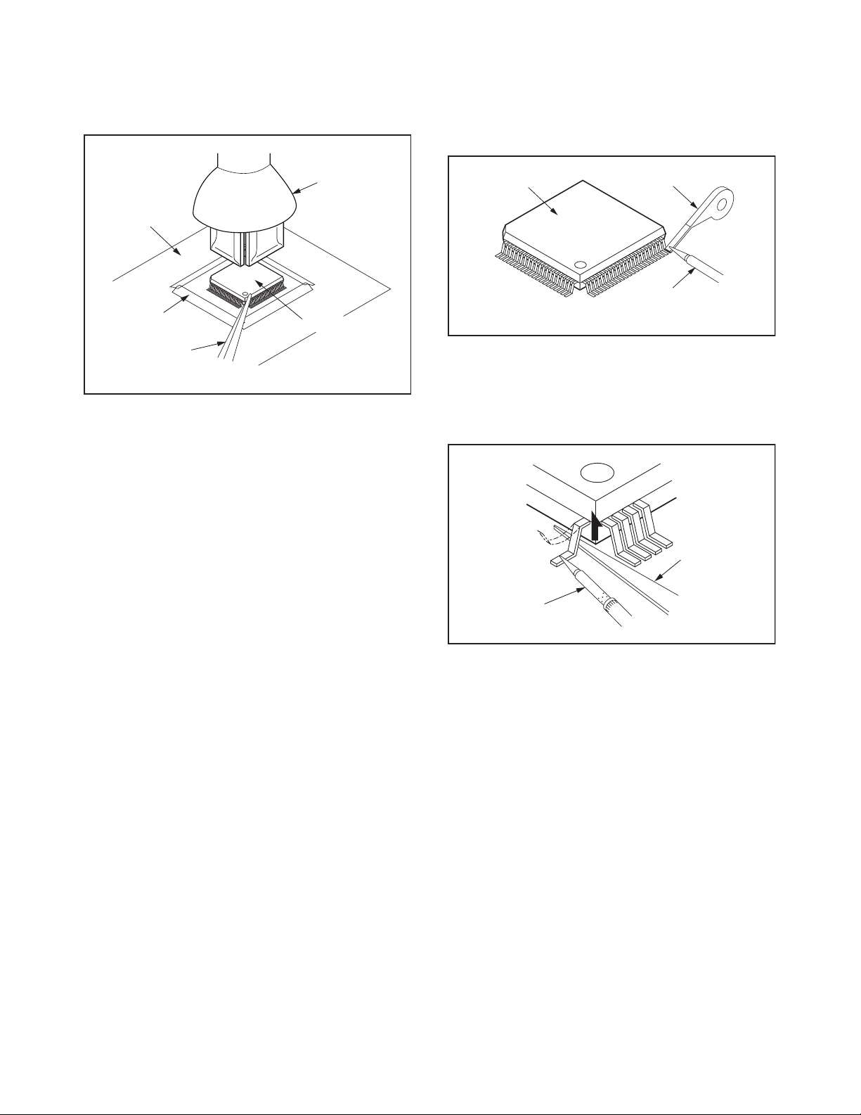
How to Remove / Install Flat Pack-IC
1. Removal
With Hot-Air Flat Pack-IC Desoldering Machine:
1. Prepare the hot-air flat pack-IC desoldering
machine, then apply hot air to the Flat Pack-IC
(about 5 to 6 seconds). (Fig. S-1-1)
Fig. S-1-1
Instructions for Connectors
1. When you connect or disconnect the FFC (Flexible
Foil Connector) cable, be sure to first disconnect
the AC cord.
2. FFC (Flexible Foil Connector) cable should be
inserted parallel into the connector, not at an
angle.
FFC Cable
Connector
CBA
* Be careful to avoid a short circuit.
2. Remove the flat pack-IC with tweezers while
applying the hot air.
3. Bottom of the flat pack-IC is fixed with glue to the
CBA; when removing entire flat pack-IC, first apply
soldering iron to center of the flat pack-IC and heat
up. Then remove (glue will be melted). (Fig. S-1-6)
4. Release the flat pack-IC from the CBA using
tweezers. (Fig. S-1-6)
CAUTION:
1. The Flat Pack-IC shape may differ by models. Use
an appropriate hot-air flat pack-IC desoldering
machine, whose shape matches that of the Flat
Pack-IC.
2. Do not supply hot air to the chip parts around the
flat pack-IC for over 6 seconds because damage
to the chip parts may occur. Put masking tape
around the flat pack-IC to protect other parts from
damage. (Fig. S-1-2)
1-4-1 BDN_SN
Page 8
3. The flat pack-IC on the CBA is affixed with glue, so
be careful not to break or damage the foil of each
pin or the solder lands under the IC when
removing it.
With Soldering Iron:
1. Using desoldering braid, remove the solder from
all pins of the flat pack-IC. When you use solder
flux which is applied to all pins of the flat pack-IC,
you can remove it easily. (Fig. S-1-3)
CBA
Masking
Ta pe
Tweezers
Hot-air
Flat Pack-IC
Desoldering
Machine
Flat Pack-IC
Fig. S-1-2
Flat Pack-IC
Desoldering Braid
Soldering Iron
Fig. S-1-3
2. Lift each lead of the flat pack-IC upward one by
one, using a sharp pin or wire to which solder will
not adhere (iron wire). When heating the pins, use
a fine tip soldering iron or a hot air desoldering
machine. (Fig. S-1-4)
Sharp
Pin
Fine Tip
Soldering Iron
3. Bottom of the flat pack-IC is fixed with glue to the
CBA; when removing entire flat pack-IC, first apply
soldering iron to center of the flat pack-IC and heat
up. Then remove (glue will be melted). (Fig. S-1-6)
4. Release the flat pack-IC from the CBA using
tweezers. (Fig. S-1-6)
Fig. S-1-4
1-4-2 BDN_SN
Page 9
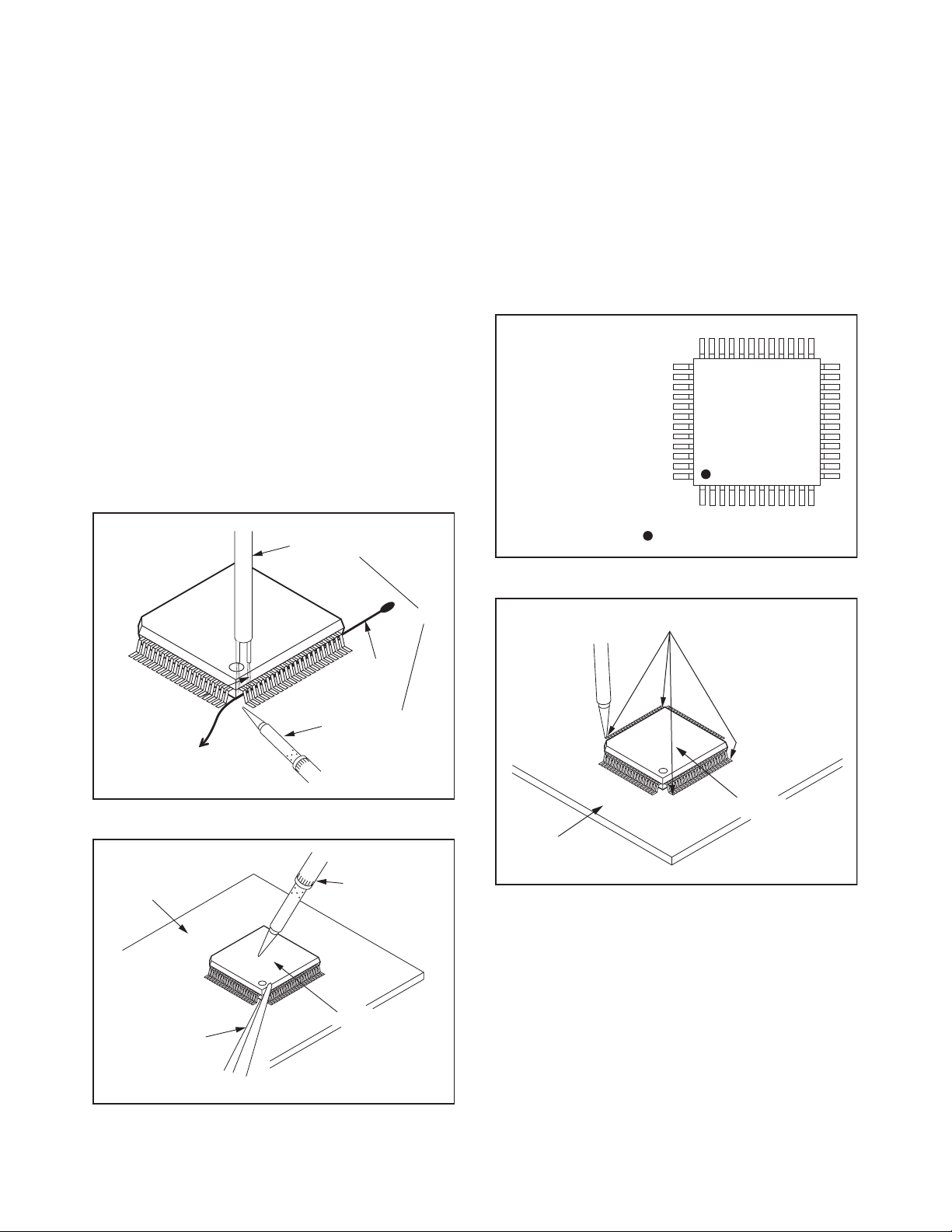
With Iron Wire:
1. Using desoldering braid, remove the solder from
all pins of the flat pack-IC. When you use solder
flux which is applied to all pins of the flat pack-IC,
you can remove it easily. (Fig. S-1-3)
2. Affix the wire to a workbench or solid mounting
point, as shown in Fig. S-1-5.
3. While heating the pins using a fine tip soldering
iron or hot air blower, pull up the wire as the solder
melts so as to lift the IC leads from the CBA
contact pads as shown in Fig. S-1-5.
4. Bottom of the flat pack-IC is fixed with glue to the
CBA; when removing entire flat pack-IC, first apply
soldering iron to center of the flat pack-IC and heat
up. Then remove (glue will be melted). (Fig. S-1-6)
5. Release the flat pack-IC from the CBA using
tweezers. (Fig. S-1-6)
Note: When using a soldering iron, care must be
taken to ensure that the flat pack-IC is not
being held by glue. When the flat pack-IC is
removed from the CBA, handle it gently
because it may be damaged if force is applied.
Hot Air Blower
2. Installation
1. Using desoldering braid, remove the solder from
the foil of each pin of the flat pack-IC on the CBA
so you can install a replacement flat pack-IC more
easily.
2. The “ I ” mark on the flat pack-IC indicates pin 1.
(See Fig. S-1-7.) Be sure this mark matches the
pin 1 on the PCB when positioning for installation.
Then presolder the four corners of the flat pack-IC.
(See Fig. S-1-8.)
3. Solder all pins of the flat pack-IC. Be sure that
none of the pins have solder bridges.
Example :
Pin 1 of the Flat Pack-IC
is indicated by a " " mark.
Fig. S-1-7
To Solid
Mounting Point
CBA
Tweezers
Iron Wire
Soldering Iron
Fig. S-1-5
Fine Tip
Soldering Iron
Flat Pack-IC
or
Presolder
Flat Pack-IC
CBA
Fig. S-1-8
Fig. S-1-6
1-4-3 BDN_SN
Page 10
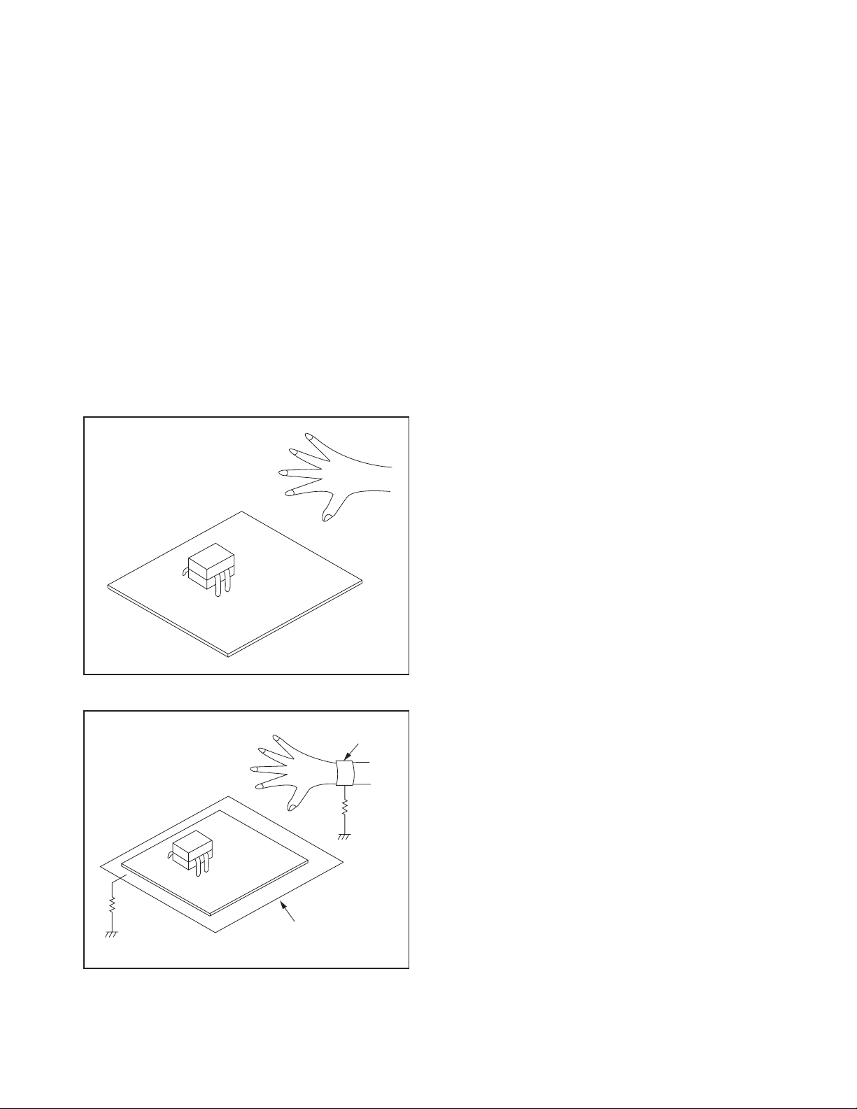
Instructions for Handling Semiconductors
Electrostatic breakdown of the semi-conductors may
occur due to a potential difference caused by
electrostatic charge during unpacking or repair work.
1. Ground for Human Body
Be sure to wear a grounding band (1 MΩ) that is
properly grounded to remove any static electricity that
may be charged on the body.
2. Ground for Workbench
Be sure to place a conductive sheet or copper plate
with proper grounding (1 MΩ) on the workbench or
other surface, where the semi-conductors are to be
placed. Because the static electricity charge on
clothing will not escape through the body grounding
band, be careful to avoid contacting semi-conductors
with your clothing.
<Incorrect>
<Correct>
1MΩ
CBA
Grounding Band
1MΩ
CBA
Conductive Sheet or
Copper Plate
1-4-4 BDN_SN
Page 11
CABINET DISASSEMBLY INSTRUCTIONS
1. Disassembly Flowchart
This flowchart indicates the disassembly steps to gain
access to items to be serviced. When reassembling,
follow the steps in reverse order. Bend, route, and
dress the cables as they were originally.
[1] Top Cover
[2] Tray
Assembly
[5] Front-B CBA
[10] Audio CBA
[3] Front
Assembly
[6] Front Bracket
[9] Rear Panel
[11] Video CBA
[12] AV PCB
Bracket
[13] BD Main CBA
& BD Mechanism
Assembly
[14] BD Main
CBA Unit
[15] BD Mechanism
Assembly
[18] Loader
Bracket
[4] Front-A CBA
[7] Inlet CBA
[8] RS232C
CBA
[16] Power
Supply CBA
[17] Power
Holder
2. Disassembly Method
ID/
Loc.
Part
No.
[1] Top Cover D1 9(S-1) ---
Tr ay
[2]
Assembly
Front
[3]
Assembly
Front-A
[4]
CBA
Front-B
[5]
CBA
Front
[6]
Bracket
[7]
Inlet CBA
RS232C
[8]
CBA
Fig.
No.
Removal
Note
D2 --------------- 1
2(L-1), (L-2), 5(S-2),
D2
9(S-3), CN2002
D2 CN3001 ---
D2 --------------- ---
D3 7(S-4) ---
D4 (S-5), 2(S-6), CN1002 ---
D4 (S-7), 2(S-8), CN5501 ---
2
ID/
Loc.
Part
No.
[9] Rear Panel D4
[10] Audio CBA D5
Fig.
No.
8(S-9), 2(S-10),
5(S-11)
4(S-12), CN2001,
CN2201
Removal
Note
---
[11] Video CBA D6 4(S-13), CN6901 ---
AV PCB
[12]
Bracket
D6 4(S-14) ---
BD Main
[13]
CBA & BD
Mechanism
2(S-15), 4(S-16),
D7
CN6101
---
Assembly
[14]
[15]
BD Main
CBA Unit
BD
Mechanism
Assembly
CN7001, CN7002,
D8
CN7003, Hook
4(S-17),
D8
Loader Holder
Power
[16]
Supply
D9 3(S-18), 2(S-19) ---
CBA
Power
[17]
[18]
↓
(1)
Holder
Loader
Bracket
↓
(2)
D9 3(S-20) ---
D9 6(S-21) ---
↓
(3)
↓
(4)
(5)
Note:
(1) Identification (location) No. of parts in the figures
(2) Name of the part
(3) Figure Number for reference
(4) Identification of parts to be removed, unhooked,
unlocked, released, unplugged, unclamped, or
desoldered.
P = Spring, L = Locking Tab, S = Screw,
CN = Connector
e.g. 2(S-2) = two Screws of (S-2),
2(L-2) = two Locking Tabs of (L-2)
(5) Refer to “Reference Notes.”
3
4
4
↓
1-5-1 E5WB0DC
Page 12
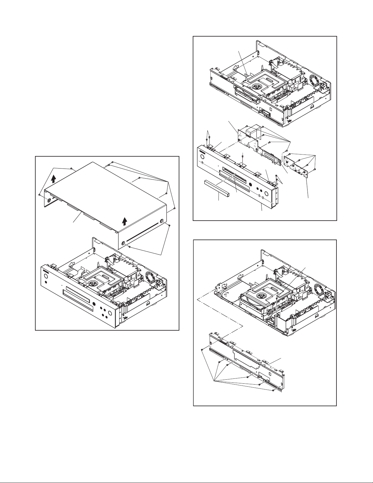
Reference Notes
1. How to remove Tray Assembly
1) Press the [A] button to open the tray.
2) Remove the Tray Assembly.
3) Press the [A] button to close the tray.
2. CAUTION 1: Locking Tabs (L-1) and (L-2) are
fragile. Be careful not to break them.
3. When reassembling, be sure to use the original
screws or specified screws listed in the parts
list.
4. When replacing the BD Mechanism Assembly
or BD Main CBA Unit, refer to “ADJUSTMENT
INSTRUCTIONS FOR BD MAIN CBA OR BD
MECHANISM ASSEMBLY REPLACEMENT.”
(S-1)
CN2002
[4] Front-A CBA
(S-2)
(L-1)
(S-2)
(S-3)
(S-3)
(L-1)
[1] Top Cover
(S-1)
(S-1)
Fig. D1
[2] Tray
Assembly
(L-2)
[3] Front Assembly
CN3001
(S-2)
[5] Front-B CBA
Fig. D2
(S-4)
[6] Front Bracket
(S-4)
Fig. D3
1-5-2 E5WB0DC
Page 13
[9] *Rear Panel
(S-11)
[8] RS232C
CBA
CN5501
*See Reference Note 3.
(S-9)
(S-7)
(S-8)
(S-10)
CN1002
(S-11)
(S-9)
(S-11)
[7] Inlet CBA
Fig. D4
(S-5)
(S-6)
[11] Video CBA
(S-14)
[12] AV PCB
Bracket
(S-13)
(S-14)
CN6901
Fig. D6
CN2001
(S-12)
[10] Audio CBA
CN2201
Fig. D5
[13] BD Main CBA &
BD Mechanism
Assembly
(S-16)
(S-15)
CN6101
Fig. D7
1-5-3 E5WB0DC
Page 14
(S-17)
[15] *BD Mechanism
Assembly
(S-18)
(S-19)
[16] Power Supply
CBA
[17] Power Holder
Loader Holder
CN7003
CN7001
CN7002
[14] *BD Main CBA Unit
* See Reference Note 4.
Hook
(S-20)
(S-21)
(S-21)
[18] Loader
Bracket
Fig. D8
Fig. D9
1-5-4 E5WB0DC
Page 15
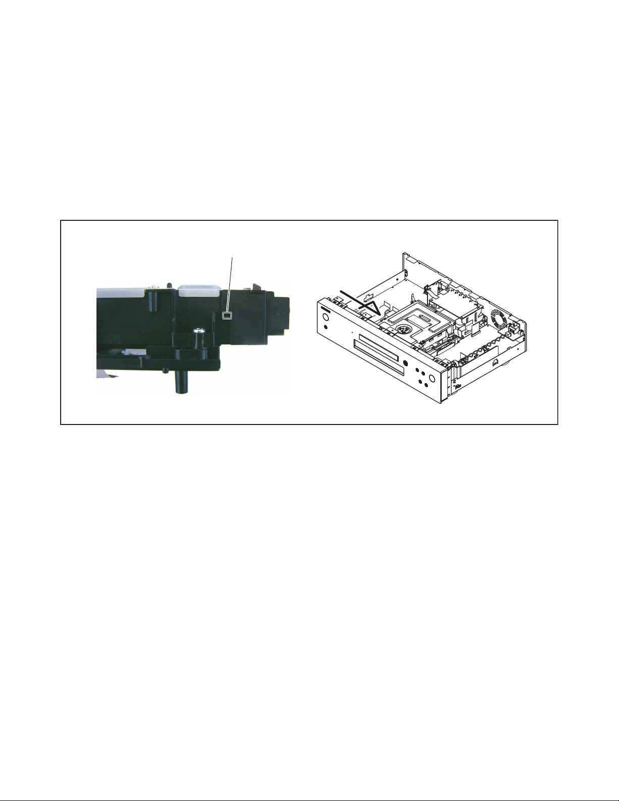
3. How to Eject a Disc
When a disc cannot be removed due to malfunction or when an unplayable disc is inserted, follow the
procedure below to remove the disc.
Procedure A
1. Unplug the AC power cord and then plug it in.
2. Turn the power on by pressing the [A] button and the disc tray will open automatically.
Procedure B
1. Remove the Top Cover.
2. Insert a screwdriver, etc. into the hole (as shown below) straight and gently until the tray is ejected.
3. Pull the tray out manually and remove the disc.
Hole
A
View for A
1-5-5 E5WB0DC
Page 16

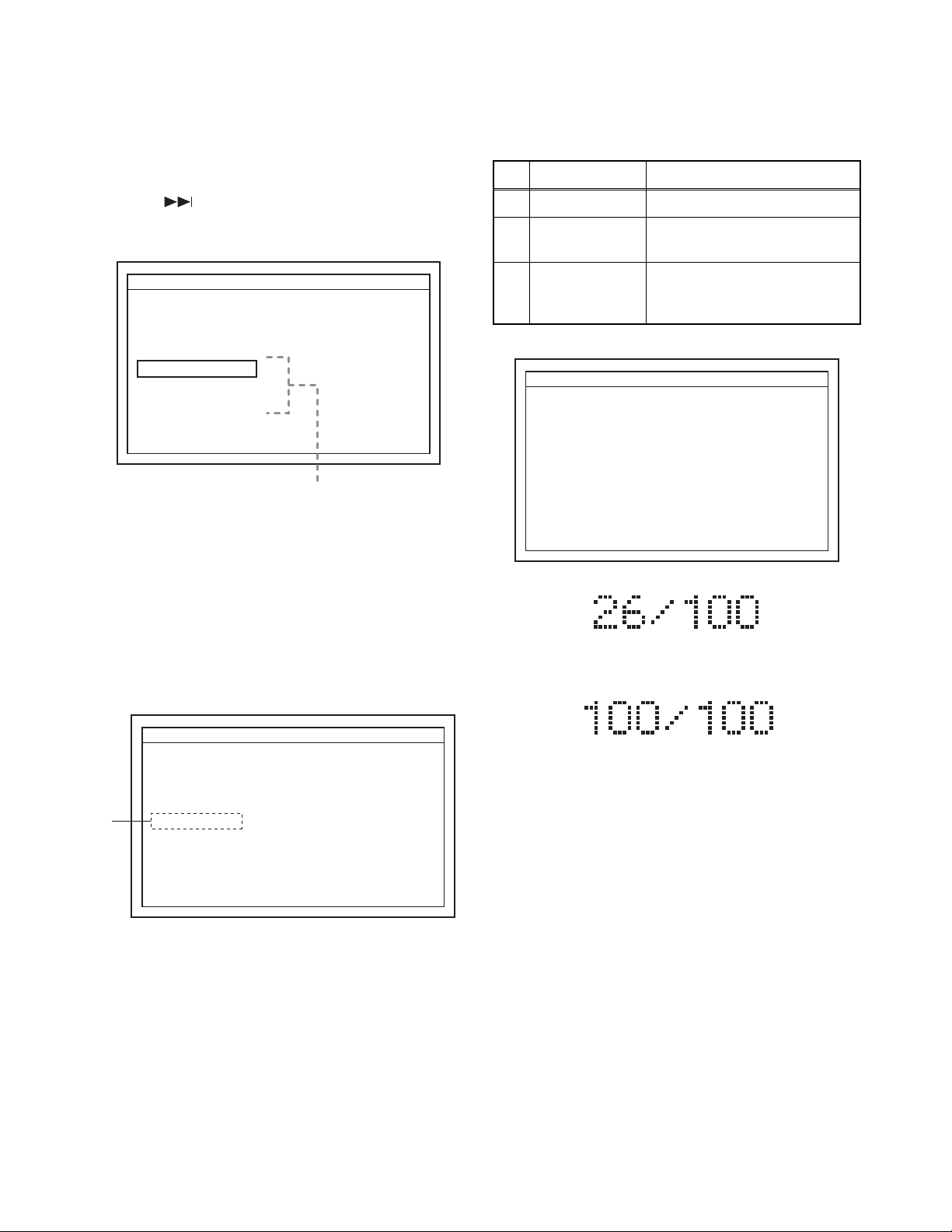
HOW TO INITIALIZE THE BLU-RAY DISC PLAYER
To put the program back at the factory-default,
initialize the BD player as the following procedure.
Note:
• By initializing, network is reset to disconnected state
and “Network Service Disclaimer” appears on the
screen.
1. Turn the power on.
2. Remove the disc on the tray and close the tray.
3. Press [ ] (skip up), [1], [2], and [3] buttons on
the remote control unit in this order.
Fig. a appears on the screen. All VFD lights.
"*" differ depending on the models.
Version Display
F/W Name
Version
Region
Pickup
ESN
DRM
Default Setting : --
Default Setting : STOP End : STANDBY-ON
VFD/LED Check : OK
: *******
: *.**.**
: *-*
: **
: ********************************
: OK
Fig. a
4. Press [ C ] button on the remote control unit.
Fig. b appears on the screen and Fig. c appears
on the VFD.
"*" differ depending on the models.
Version Display
F/W Name
Version
Region
Pickup
ESN
DRM
Default Setting : SUCCESS
Default Setting : STOP End : STANDBY-ON
VFD/LED Check : OK
: *******
: *.**.**
: *-*
: **
: ********************************
: OK
Fig. b
Fig. c
5. After initializing, the power will turn off
automatically.
1-6-1 E5WF0INT
Page 17
FIRMWARE RENEWAL MODE
Note: The file extension of the available firmware is
“b40”.
1. Turn the power on and remove the disc on the tray
and close the tray.
2. Press [ ] (skip up), [6], [5], and [4] buttons on
the remote control unit in that order.
Fig. a appears on the screen.
"*" differ depending on the models.
F/W Version Mode
Please select software update mode.
Disc
USB
SD Card
The available software update mode will
differ depending on the model type.
F/W Name : ******* Ver *.**.**
Fig. a Version Up Mode Screen (Example)
3. Select “Disc” or “USB” and press [ENTER] button
on the remote control unit. The tray will open
automatically, if “Disc” is selected.
4. Insert the disc or USB Flash Drive for version up.
5. The BD player enters the F/W version up mode
automatically. Fig. b will appear on the screen.
Make sure to insert the proper F/W for the state of
this model.
"*" differ depending on the models.
The appearance shown in (*1) of Fig. b is
described as follows:
No. Appearance State
1 Loading Disc Loading the disc
2 Reading...
Sending files into the
memory.
Writing new version data,
3 See FLD.
the progress will be displayed
as shown in Fig. d.
"*" differ depending on the models.
F/W Version Mode
1. ALL
Version : *.**.**
CHECKSUM : ****
See FLD.
The unit will automatically turn off when update is completed,
and automatically turns back on.
F/W Name : ******* Ver *.**.**
***************.b40
Fig. c Version Up Mode
Fig. d VFD in Version Up Mode
6. After the update, Fig. e will appear on the VFD and
the power will turn off automatically.
(*1)
F/W Version Mode
Loading Disc...
F/W Name : ******* Ver *.**.**
Fig. b Programming Mode Screen (Example)
Fig. e
VFD upon Finishing the Programming Mode (Example)
7. The power turns on automatically. If disc mode
was selected, the tray will open automatically.
Remove the disc or USB Flash Drive from the unit.
Note: All the settings will be put back to factory-
default.
The following USB Flash Drive can be used for
software update. Make sure to use a device that has
enough space.
• USB Flash Drive (FAT16/FAT32 file system)
• Choose “USB” at Fig. a. when using a SD Card that
is connected to a Card Reader. Otherwise, the unit
will not be updated if “SD Card” is selected.
1-7-1 E5WF0FW
Page 18

How to Verify the Firmware Version
1. Turn the power on.
2. Remove the disc on the tray and close the tray.
3. Press [ ] (skip up), [1], [2], and [3] buttons on
the remote control unit in that order.
Fig. f appears on the screen. All VFD lights.
"*" differ depending on the models.
Version Display
F/W Name
Version
Region
Pickup
ESN
DRM
Default Setting : --
Default Setting : STOP End : STANDBY-ON
VFD/LED Check : OK
4. To exit this mode, press [ ] button.
: *******
: *.**.**
: *-*
: **
: ********************************
: OK
Fig. f
1-7-2 E5WF0FW
Page 19
ADJUSTMENT INSTRUCTIONS FOR BD MAIN CBA OR
BD MECHANISM ASSEMBLY REPLACEMENT
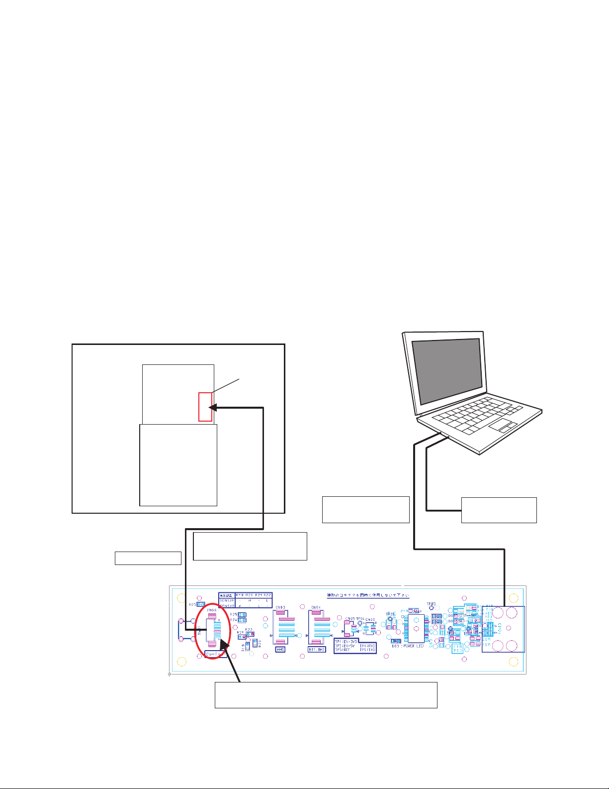
When replacing either BD Main CBA or BD Mechanism Assembly, the unique OPU DATA of the BD Mechanism
needs to be written into the BD Main CBA. Follow the procedure below for OPU DATA write operation.
Equipments:
• PC (OS: Windows XP strongly recommended)
• Barcode reader
• COMTOOL jig relay board + 6PIN FFC cable
• USB cable Type AB
• Device driver for COMTOOL jig (CDM 2.06.00 WHQL Certified)
• Specialized application (OpuDataWriter)
Caution:
Always turn the unit power off before connecting the FFC cable or removing the FFC cable from the BD Main CBA
•
1. Preparation Of Work Environment
1-1.
For the OPU DATA write operation, refer to the connection diagram and connect each device as shown below.
Connection Diagram
Note: The unit configuration may differ depending on model types.
.
Unit (Completed product)
BD Main CBA
BD Mechanism
Assembly
6-pin FFC cable
6-pin
connector
Connect to 6-pin connector
of BD Main CBA
COMTOOL Jig Relay Board
USB cable Type AB
(To USB Port)
PC
Barcode Reader
(To USB Port)
Location of Pin 1 on COMTOOL Jig Relay Board
Lower side of Ref. No CN06 is pin 1 (printed 1 by silk)
1-8-1 E5WF0_(3D)_AIR
Page 20
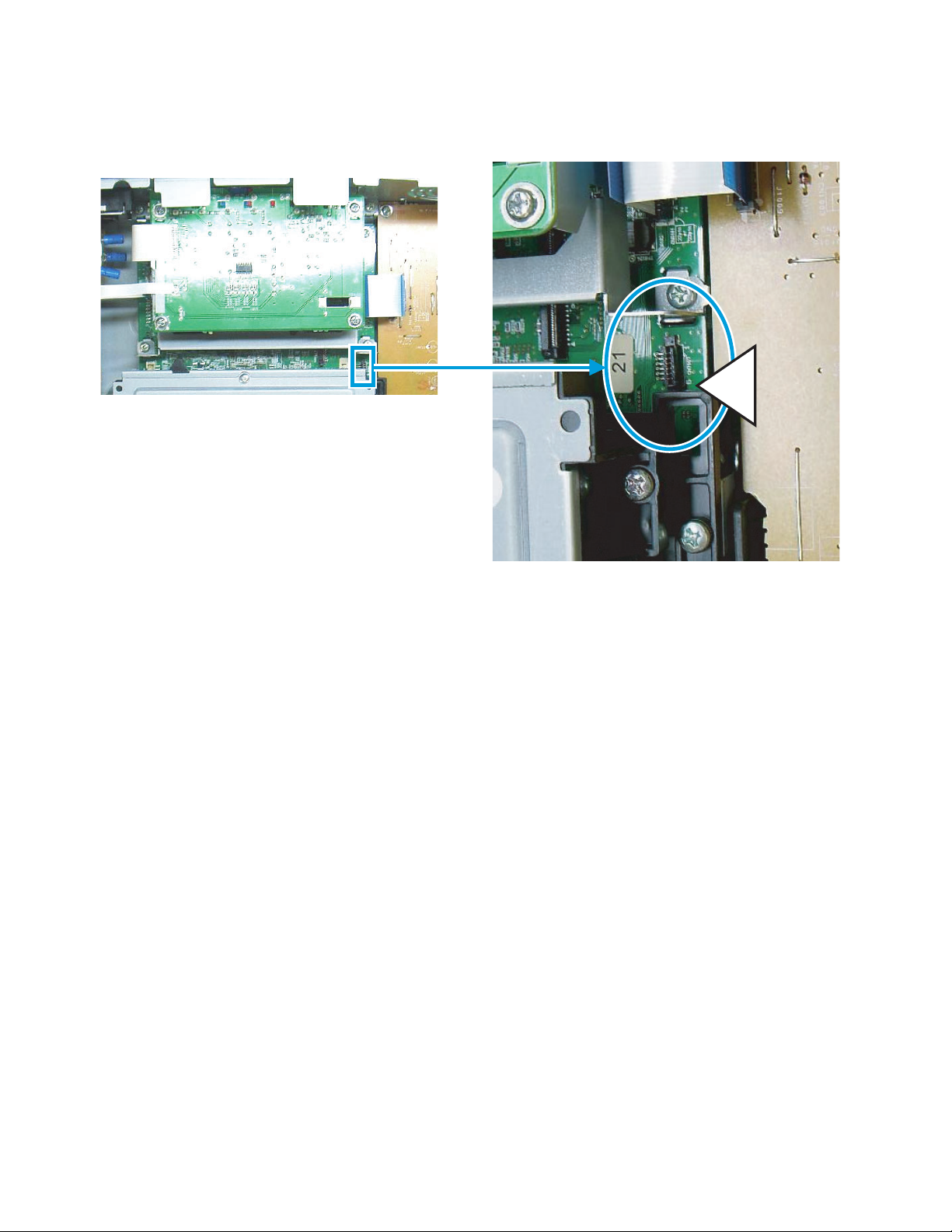
Caution:
• Make sure the FFC cable is inserted in the proper direction so the Pin 1 of COMTOOL jig relay board and Pin 1
of BD MAIN CBA connector is connected.
Location of Pin 1 on BD Main CBA
1pin
Pin 1 is located on the front side
• If the device driver (CDM 2.06.00 WHQL Certified) of COMTOOL jig relay board is not installed in the PC, install
this before connecting COMTOOL jig relay board to the PC.
<How to install the device driver for COMTOOL jig relay board>
1) Save the device driver for COMTOOL jig relay board in the C: drive.
2) Connect COMTOOL jig relay board to the PC.
3) The driver installation screen opens. Select [Install from a list or specific location (Advanced)] then click
[Next].
4) Select [Search for the best driver in these locations.] then check the box for [Include this location in the
search:].
5) Click on Browse button then select the device driver (CDM 2.06.00 WHQL Certified) folder in the C: drive.
Click [Next].
6) Confirm that installation of [USB Serial Converter] device driver has completed and click on [Finish].
2. How To Check Which Port Is Used For COMTOOL Jig Relay Board
2-1. Click on the Windows [Start] button on the PC.
2-2. Right click on [My Computer].
2-3. Click on [Properties].
2-4. Click on [Hardware] tab in System Properties window.
2-5. Click on [Device Manager].
2-6. Click on [Ports (COM&LPT)].
2-7. Check which connection port is assigned for [USB Serial Port] (e.g. COM1).
The connection port number assigned here will be used later during setup of application.
3. Application Setup
3-1. Save the application folder (OpuDataWriter) directly under the C: drive.
3-2. Create a shortcut for [OpuDataWriter.exe] which is located inside the folder on the desktop.
1-8-2 E5WF0_(3D)_AIR
Page 21
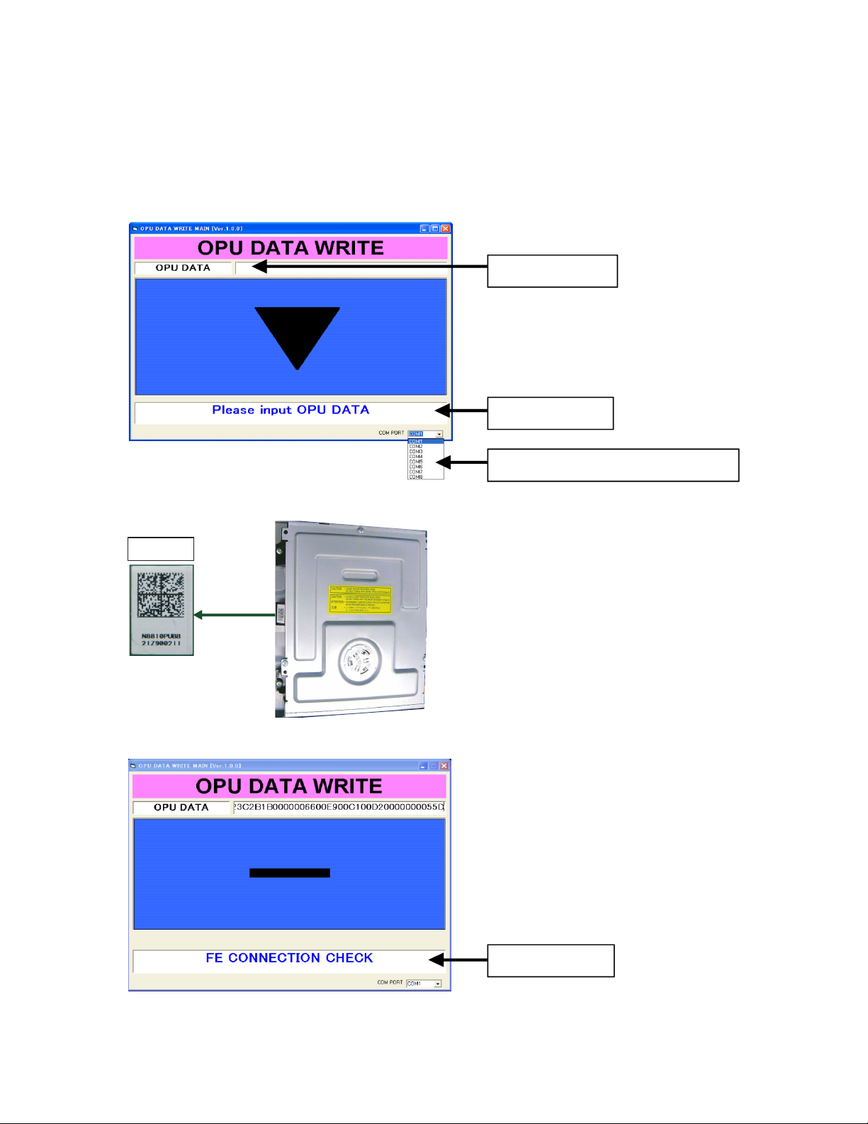
4. OPU DATA WRITE
4-1. Connect the unit’s AC power cord. Wait for about 30 seconds until the unit is in standby mode.
4-2. Double click on the [OpuDataWriter.exe] shortcut on the desktop to start the application.
4-3. Application start screen appears.
Select the assigned connection port of [USB Serial Port] for the [COM PORT] field located at the right corner
of the screen.
Check that [Please input OPU DATA] message is displayed in the Status Display.
Set the cursor position at the blank box next to the [OPU DATA].
Cursor position
Status Display
Select the assigned COM PORT
4-4. Using the Barcode reader, scan the QR code attached to the BD Mechanism Assembly.
QR Code
4-5. Check that [FE CONNECTION CHECK] message appears on the Status Display then turn the unit power on.
Status Display
If error occurs:
If an error occurs, the screen changes to a red display. In such case, close the window and then unplug the
unit AC power cord. Check if each device is properly connected then repeat from step 1.
1-8-3 E5WF0_(3D)_AIR
Page 22

4-6. Data write begins. While writing data, the Status Display message will change.
SEND LD PAR
Status Display
4-7. [OK] appears in the Status Display if data write has been completed successfully.
If error occurs:
• If an error occurs, the screen changes to a red display. In such case, close the window and then unplug the
unit AC power cord. Check if each device is properly connected then repeat from step 1.
• If an error other than connection error occurs for more than 3 times, the BD MAIN CBA or BD Mechanism
Assembly may be defected. Replace with a new one before performing the OPU DATA write.
4-8. After data write has been completed successfully, unplug the AC power cord.
4-9. Remove the FFC Cable of COMTOOL jig relay board connected to the BD Main CBA.
Then disconnect all devices connected to the unit.
1-8-4 E5WF0_(3D)_AIR
Page 23

Error Code
Error Code Error Description
10 Start word error The first letter entered for [LOADER S/N] does not match.
101 [ReadBackup]Drive Mount error Cannot mount the drive set for [ReadBackup] folder.
102 [Transfer]Drive Mount error Cannot mount the drive set for [Transfer] folder.
103 [OpuData]Drive Mount error Cannot mount the drive set for [OpuData] folder.
104 [Log]Drive Mount error Cannot mount the drive set for [Log] folder.
210 Start word error The first letter entered for [OPU DATA] does not match.
300 CheckSum NG
301 QRCheckSum NG [Process1]CheckSum Test error.
310 CreateHeader NG [Process2]Error creating Header region.
320 CreateLDD NG [Process3]Error creating LDD region.
330 CreateFBIAS NG [Process4]Error creating FBIAS region.
340 CreateExp NG [Process5]Error creating EXP region.
350 CreateLcd NG [Process6]Error creating LCD region.
360 CreateCrc NG [Process7]Error creating CRC region.
370 CreateDDD NG [Process8]Error creating DDD file.
380 CreateLog NG [Process9]Error creating LOG file.
390 CreateOpuData NG [Process10]Error creating OPU DATA file.
1010 Start word error The first letter entered for [LOADER S/N] does not match.
1130 DDDFile not found
1140 DDDFile search error Error occurred while searching DDD file in [WriteBackup] folder.
1151 [WriteBackup]Drive Mount error Cannot mount the drive set for [WriteBackup] folder.
1152 [Transfer]Drive Mount error Cannot mount the drive set for [Transfer] folder.
1153 [OpuData]Drive Mount error Cannot mount the drive set for [OpuData] folder.
1154 [Log]Drive Mount error Cannot mount the drive set for [Log] folder.
1210 ComConnection TIME OUT
1211 Tray Close error Cannot close tray.
1220 TestUnitReady ERROR0 [ERROR0] returned for TestUnitReady command issued.
1221 TestUnitReady ERROR1 [ERROR1] returned for TestUnitReady command issued.
1222 TestUnitReady TIME OUT No reply received for TestUnitReady command issued.
1230 ReadVirRAM32 NG
1240 WriteReg16 NG
1250 WriteReg1 NG
1260 FlashWrite ERROR0 [ERROR] returned for FlashWrite command issued.
1261 FlashWrite ERROR1 [ERROR] returned for FlashWrite command issued.
1262 FlashWrite TIME OUT No reply received for FlashWrite command issued.
1310 MoveDDDFile NG [Move DDD file to written folder]Process Error
1320 CreateLog NG [Create LOG file]Process Error
1330 CreateComLOG NG [COM PORT connection LOG file create]Process Error
1400 TIME OUT System Time Out
2031 LdParamSend NG LD Parameter Send Error
The checksum of the entered OPU DATA(QR code) does not
match.
As a result of searching DDD file in the [WriteBackup] folder, the
entered DDD file for [LOADER S/N] could not be found.
No reply received for NOP commmand (20 times at 500mSec
interval).
[Acquire DRAM head address of DDD data forwarding
region]Process Error
[Send ddd data to DRAM head address region(16BYTE unit)]
Process Error
[Send ddd data to DRAM head address region(1BYTE
unit)]Process Error
1-8-5 E5WF0_(3D)_AIR
Page 24

Error Code Error Description
2042 LdParamClear ERROR0 Cannot initialize LD Parameter.
2043 LdParamClear ERROR1 Cannot initialize LD Parameter.
2044 LdParamClear TIME OUT Cannot initialize LD Parameter (TimeOut).
2051 IopSet NG Iop Set Error
2052 IopSet ERROR0 Iop Set Error
2053 IopSet ERROR1 Iop Set Error
2054 IopSet TIME OUT lop Set Error (TimeOut)
2055 IopSet ERROR0 Iop Set Error
2056 IopSet ERROR1 Iop Set Error
2057 IopSet TIME OUT lop Set Error (TimeOut)
2058 CD Iop LIMIT NG CD Iop exceeds limit value.
2059 DVD Iop LIMIT NG DVD Iop exceeds limit value.
2060 BD Iop LIMIT NG BD Iop exceeds limit value.
2081 LdParamVerify NG LD Parameter Verify Error
2091 AtapiComCheck NG BE start Error.
2101 ID4 OFF NG Cannot set ID4 OFF.
2111 SET BOR RATE NG Failed to change Serial Connection Rate.
2200 Genaration NG Generation detect failure.
6001 Factory Info save Error Failed to create FactoryInfo file.
6002 Factory Info save Error Failed to create FactoryInfo file.
6100 Factory Info save Error Failed to create FactoryInfo file.
5. Saving The Pre-Operation OPU DATA
OPU DATA before performing the OPU DATA write is saved in a folder automatically.
5-1. When the OPU DATA write operation has been completed successfully, a folder named [FactoryInfo] is
created in the application folder (OpuDataWriter).
5-2. In the [FactoryInfo] folder, a folder is created monthly in which text file data are saved.
This text file is created with a file name of the OPU serial number and contains the pre-operation OPU DATA.
Pre-operation OPU DATA text file
Year(2010)Month(12)
5-3. The text file is necessary for analyzing the defective BD Mechanism. Submit this text file with the defective
BD Mechanism as necessary to the appropriate managing Department.
1-8-6 E5WF0_(3D)_AIR
Page 25

ERROR MESSAGE
Note: Only error messages for the unit’s corresponding media will appear.
Disc Error
Playback feature may not be available on this Disc.
Error Message
Disc Error
Loader Error
- - Please eject the disc. - -
Disc Error
- - Please eject the disc. - Playback feature may not be available on this Disc.
Loader Error
The unit stopped automatically due to loader error.
Please open the disc tray once and then close it.
Parental Lock Error
Region Error
The device connected for HDMI
connection does not support HDCP.
USB Error
BD-Live Network Connecting Error
LAN Cable Not Connected
Cannot Acquire DHCP Server
Cannot Acquire IP Address
Already Existing IP Address
Parental Lock On
The current selected parental level prohibits playback.
Region Error
Playback is not authorized in your region.
Region code of this disc :
(There is no message.)
The following error will appear on the VFD.
Memory Device Error
- - Please check the Memory Device. - There is no playback file on the Memory Device or Device has incorrect/
no format.
BD-Live Setting Error
Network connection is interrupted. Please confirm “BD-Live Setting”.
The cable is not connected.
Please confirm the connection of the cable.
DHCP cannot be acquired.
Please confirm connection or set it with the manual operation.
Internet Protocol address is not set.
Please confirm the set content.
The equipment with same Internet Protocol address already exists.
Please set another Internet Protocol address.
No Response From Default
Gateway
Cannot Connect To DNS Server
There is no response from Default gateway.
Please confirm the address of Default gateway.
It is not possible to connect to the DNS server.
Please confirm the Internet connection or the DNS address setting.
1-9-1 E5WF0ER
Page 26

Error Message
Cannot Connect To Server
Cannot Confirm Firmware Version
Firmware Update Error
(Update File Error)
Cannot Connect To Download
Server
USB Error
It is not possible to connect to the server.
Please contact our support center.
It is not possible to confirm the software version.
Please contact our support center.
Error detected.
File may be corrupted.
Please download software again.
Error detected.
Please confirm whether it is USB device that corresponds to software
update.
It is not possible to connect to the server.
Please contact our support center.
Error in the USB Connection. USB operation has been stopped
automatically. Please remove the USB device and restart the unit.
1-9-2 E5WF0ER
Page 27

HOME NETWORK (DLNA) ERROR CODE
Error Code appears in the error screen when the unit
detects an error, as shown below. The code is used to
specifically determine the cause of error.
Network Error
Cannot connected to server. Please check your settings.
Press [OK].
NE [00202010]
Error CodeError message
Fig. 1: Error Code (Example)
Error Code are displayed with “NE[********]” (“*” is
error code) as shown above.
Error Code Form
In the Home Network (DLNA), Error Code are used as
follows.
002XXXXX
Detailed Error Code
Summary Error Code
Fig. 2
“Summary Error Code” are shown in the list below.
Summary
Error Code
02
03 Playback Error
05 No playable files found.
20 System Error
21
22 List Updated.
23 Connection with server lost.
24
Cannot connect to server. Please
check your settings.
Unable to display files from the
server. Please check server
settings.
Unable to connect to more than 10
servers. Please turn off or stop
broadcasting 1 or more servers.
Error message
1-10-1 E5WF0DLNAER
Page 28

Detailed Error Code table (DLNA – HTTP Status Code)
Status Code Description
201 Created A new resource was created by this unit’s request.
202 Accepted This unit’s request was accepted but its processing is not completed.
204 No Content Though the server processed the request, there was no content.
205 Reset Content No content.
• There are multiple choices.
• The server could not determine its response.
300 Multiple Choices
301 Moved Permanently
302 Found
• Requested information contains multiple representations.
This status is handled as Redirection by default and complies with the content
of Location HEAD related to this response.
• Moved Permanently.
• Requested resource has been assigned to a new permanent URI (Uniform
Resource Identifier). Any future references to this source must use one of the
returned URIs.
• Indicates that requested information is moved to the URI specified by the
Location HEAD. When this status is received, the default action is tracking
the Location HEAD related to the response. When the original request
method is POST, the redirected request will use GET.
• Found.
• Requested resource resides temporarily under a different URI.(Uniform
Resource Identifier)
• Indicates that requested information exists in the URI specified by the Location HEAD. When this status is received, Location HEAD related to the
response will be tracked by default. When the request method is POST the
redirected request will use GET.
• See other.
• The response to the request can be found under a different URI (Uniform
Resource Identifier) and to get this response, GET HTTP method will be
303 See Other
304 Not Modified
305 Use Proxy
400 Bad Request The server could not understand this unit’s request.
401 Unauthorized Indicates that the resource requested by this unit requires authentication.
403 Forbidden The server received this unit’s request, but refused to fulfill it.
404 Not Found The requested URI was not found.
405 Method Not Allowed
406 Not Acceptable
used.
• As a result of POST, client will be automatically redirected to the URI specified by the Location HEAD. GET will be used for requesting to a resource
specified by the Location HEAD.
This unit caches the latest resource and the requested resource is not
modified. (exception protocol error)
• Proxy will be used.
• The requested resource must be accessed through the proxy specified by the
Location field.
• Indicates that request must use the URI given by the Location HEAD to use
the proxy server.
• The method is not allowed.
• The HTTP behavior used is not allowed.
• Indicates that request method (POST or GET) is not allowed by the
requested resource.
• The client could not find an acceptable response.
• Indicates that the client specifies not to accept arbitrary representation for
Accept header which could be used by the resource.
1-10-2 E5WF0DLNAER
Page 29

Status Code Description
407 Proxy Authentication
Required
408 Request Timeout
409 Conflict
410 Gone
411 Length Required
412 Precondition Failed
• Proxy authentication is required.
• Indicates that the requested proxy will request authentication. Proxy-authenticate header contains the detailed method for authentication.
• While waiting for request, the server timed out.
• Indicates that the client did not send a request within the expected time by
the server.
• There is a conflict.
• The server timed out while waiting for a request.
• Indicates that the client did not send a request within the expected time by
the server.
• No longer available.
• The requested resource could not be found at the server and forwarding
address is unknown.
• Indicates that requested resource is no longer available.
• Length required.
• The server refused to accept the request where Content-Length was undefined.
• Indicates Content-length header is not defined.
• Fails to fulfill precondition.
• The precondition in one or more of the requested header field has been
tested false by the server.
• The precondition given in the request could not be fulfilled and the request
failed. Precondition can be set using If-Match, If-None-Match, If-UnmodifiedSince request header.
• The requested entity is too large.
413 Request Entity Too
Large
414 Request-URI Too Long
415 Unsupported Media
Ty pe
500 Internal Server Error Internal server error occurred.
501 Not Implemented
502 Bad Gateway
503 Service Unavailable
504 Gateway Timeout
• The server refused to process the request since the requested entity is larger
than the server is willing or able to process.
• Indicates that the request is too large for the server to process.
• The Request-URI is too long.
• The server refused to process the request because the request URI (Uniform
Resource Identifier) is too long for the server to interpret.
• Indicates that the URI is too long.
• The media type is not supported.
• The server refused to process the request because the format of request
entity is not supported by the requested resource for the requested method.
• Indicates the requested format is not supported.
The server does not support functionalities required to process the request
from this unit.
The proxy server between this unit and the server received an invalid reply from
another proxy or the original server.
• Service is unavailable.
• The service is temporarily overloaded.
• Because of overloading or maintenance, the server is temporarily unavailable.
• Gateway timed out.
• While waiting for gateway, the request timed out.
• Indicates that the intermediate proxy server has timed out while waiting for a
response from another proxy or original server.
505 Version Not Supported
• The version is not supported.
• The server refuses or does not support the version of protocol given in the
request message.
• Indicates that requested version is not supported by the server.
1-10-3 E5WF0DLNAER
Page 30

Detailed Error Code table (DLNA – Application Status Code)
Status Code Description
001 Nothing List
010 LAN Disconnect This unit’s LAN is disconnected.
020 Application Status Error Error was detected in the DLNA application’s internal state.
021 Application Status Error Error was detected in the DLNA application’s internal state.
022 Application System Error Error was detected in the DLNA application system.
023 Unsupported Audio
Format
As a result of list creation process, there is no item to be displayed from the
received data.
An unsupported audio format was discovered.
024 Server Number Over
Limit
025 Changed List The contents list currently displayed has been updated.
026 Disconnected Server The original server of the displaying contents list has been disconnected.
027 Application System Error Error was detected upon start of DLNA application.
600 Disconnected Server The original server of the contents has been disconnected.
601 Not Exist Content Content does not exist.
602 Critical Error System error.
603 Changed List The contents list has been updated at the server.
620 Not Exist Content Image content does not exist.
621 Get failure Image data get error. (an error other than HTTP status and under 500s)
622 File Open Error Image data working file open error.
623 File Read Error Image data working file read error.
624 File Close Error Image data working file close error.
625 Decode mode Error Image data decode mode error.
626 Header Error Image data header error.
627 Struct Error Image data header structural error.
628 Decode Error Image data decode error.
Discovered server numbers over limit.
629 Unsupported Format Unsupported format.
630 Unsupported Size Unsupported data size.
631 Attach Error Shared memory attach error.
632 Dettach Error Shared memory detach error.
633 Server Time Out Error Server timed out.
640 File Read Error File read error.
641 Unsupported Format Unsupported Format.
642 No Change Decode
Frame
643 Stream Get Error Stream get error.
660 File Read Error File read error.
661 Unsupported Format Unsupported format.
662 Video Analyze Error Video analyze error.
663 Audio Analyze Error Audio analyze error.
No updates of decode frame.
1-10-4 E5WF0DLNAER
Page 31

Status Code Description
664 1sec Offset Get Error 1sec offset get error.
665 Address Search Error Address search error.
680 RFS_EVENT_SOCKET_
ERROR
681 RFS_EVENT_HTTP_
RES_SERVER_
REFUSED
682 RFS_EVENT_HTTP_
RES_NOT_FOUND
683 RFS_EVENT_HTTP_
RES_SERVER_ERROR
684 RFS_EVENT_HTTP_
RES_UNEXPECTED_
CODE
685 RFS_EVENT_HTTP_
RES_RANGE_NOT_
SATISFIABLE
686 RFS_EVENT_RECV_
TIMEOUT
687 RFS_EVENT_DTCP_
ERROR
688 RFS_EVENT_DTCP_
CONNECT_ERROR
689 RFS_EVENT_DTCP_
KEY_MNG_ERROR
Socket error.
Server refusal notification.
The specified contents could not be found.
Server error.
Unexpected status code.
The specified range is not satisfiable.
Timed out while waiting for response.
RCVC internal error. (DTCP originated)
DTCP connection error.
Kx key error.
690 RFS_EVENT_
RESPONSE_DATA_
ERROR
691 RFS_EVENT_SYSTEM_
ERROR
692 RFS_EVENT_TCP_
DISCONNECTED
693 RFS_EVENT_
CONNECT_TIMEOUT
694 RFS_EVENT_RECV_
ERROR
700 Refresh Error Failed to update server list.
701 Disconnected Server The server has been disconnected while displaying contents list.
702 Server Not Found The server has been disconnected while getting contents list.
703 Server Info Error Failed to get server information while getting contents list.
704 Contents List Error Failed to get contents list.
705 Server Config Error Failed to configure server.
706 List Not Found Failed to get contents list.
707 Changed List Displayed contents list has been updated.
708 Object Not Found Neither folders or playable contents was found.
Received message is invalid.
RCVC internal error.
The TCP connection has been disconnected by the server during streaming.
Time out occurred while establishing TCP connection.
Could not receive contents.
709 Object Not Found By
Filter
Playable contents was not found by filter.
1-10-5 E5WF0DLNAER
Page 32

Status Code Description
710 Object Count Zero Nothing was found in the folder.
711 ILLEGAL Server Info The contents information from the server is invalid.
712 ILLEGAL Total Count The total counts of contents from the server is invalid.
713 Folder not Exist
714 Critical Error An error occurred on the system.
The specified folder does not exist. (The current contents list displayed has
been updated)
1-10-6 E5WF0DLNAER
Page 33

BLOCK DIAGRAMS
System Control Block Diagram
VFD
TO POWER SUPPLY
BLOCK DIAGRAM
PWSW5
TO VIDEO/AUDIO
BLOCK DIAGRAM
VIDEO-MUTE
19 20 21 22
FL3002
REMOTE
RS3002
CN2002 CN3002CN6802 CN2001
SENSOR
345
FL-SDA
FL-SCL
315
456
6
FL-STB
FL-RESET
REMOTE
12 12
P-ON+5V
16KEY-1
16
17 17
3D
D3004
Q3004
POWER
SW3008
CN3101 CN3001
FRONT-A CBA
KEY-1
2 2
(MAIN MICRO CONTROLLER)
IC6001
J26
PWSW5
CEC-IN
M25
J25
VIDEO-MUTE
X6301
CK27XI
CK27XO
L29
L30
27MHz
X'TAL
XRST
W29
RESET
IC6304
XFERST
F19
IC6305
151413
FL-SDA
FL-SCL
141312
J24
H25
FL-SCL
FL-SDA
RESET
IC6306
12
FL-STB
FL-RESET
K25
N29
FL-STB
FL-RESET
RESET
6
2
REMOTE
KEY-1
621 1
J28
P28
KEY-1
REMOTE
IC6312
3D-LED 3D-LED
K30
3D-LED
XRST-STM
P26
RESET
L25
RS232C-TXD
RESET
IC6313
AUDIO CBA
L26
RS232C-RXD
KEY
SWITCH
FRONT-B CBA
CN6901CN4002 CN4000CN5501
12131515
RS232C-RXD
RS232C-TXD
12
13
3
4
RS232C-RXD
RS232C-TXD
3
4
REMOTE
11
REMOTE
BUFFER
Q5551,Q5552
3
4
VIDEO CBA
BD MAIN CBA UNIT
JK8001
HDMI-
CONNECTOR
Q8001
(MAIN)
BUFFER
13
CEC
P-ON+3.3V
P-ON+1.5V
P-ON+1.1V
1-11-1
EV+3.3V
EV+1.1V
RS232C CBA
RS232C
IC5500
12
RS232C
INTERFACE
13
3RXD
CN5500
RS232C-
CONNECTOR
11
I/F
14
2TXD
PHOTO
IC5550
JK5550
COUPLER
REMOTE
-OUT
1
REMOTE
2
-IN
E5WB0BLS
Page 34

Digital Signal Process 1 Block Diagram
VIDEO SIGNAL AUDIO SIGNAL
(MAIN MICRO CONTROLLER/DIGITAL SIGNAL PROCESS)
IC6001
MPX
MATRIX
B27, B28
A28, A29,
A26, A27,
/LPP
WOB
B26, C26
TO DIGITAL SIGNAL
PROCESS 2 BLOCK
DIAGRAM
(IC6001)
STREAM
CONTROL
FE
DIGITAL
SIGNAL
PROCESS
RF
EQUALIZER
RF
GENERATOR
F30
B30
C29
G29
LDD-SDATA
LDD-SCLK
B22
C22
TRACKING-CONTROL
B20
27
TRACKING
ACTUATOR
IC7002(MOTOR DRIVE)
262524
DRIVE
COPY
FOCUS1-CONTROL
F20
FOCUS 1
ACTUATOR
DRIVE
23
AACS
PROTECT
FOCUS2-CONTROL
B19
29
FOCUS 2
ACTUATOR
22
BD+
DRIVE
21
CSS
CPRM
EXPA-CONTROL
C21
162815
COLLIMATE
LENS
201918
EXPB-CONTROL
B21
MOTOR DRIVE
17
41
SLED1-CONTROL
SLED2-CONTROL
F21
G21
37
38
SLED
MOTOR DRIVE
1
40
TRAY-IN
LOAD-CONTROL
A21
G22
SPINDLE-CONTROL
E21
SPINDLE-FG
C19
BD MAIN CBA UNIT
7
LOADING
MOTOR DRIVE
4
5
2
10
IC7001(MOTOR DRIVE)
242119131415161718
SPINDLE
MOTOR
DRIVE
4
12
*1: 12, 13, 16, 17
*2: 3, 4, 5, 6
CN7003
A-D *1
E-H *2
CN7002
V14
U13
W15
TRAY-IN 4
TRAY-IN
HU(+) 11
HU(-) 10
HV(+) 9
SPINDLE
MOTOR
HV(-) 8
VH(-) 5
HW(-) 6
HW(+) 7
BD MECHANISM
ASSEMBLY
E5WF0BLD1
SLD2(+) 1
SLED
CN7001
SLD1(-) 4
LOAD(-) 1
SLD1(+) 3
LOAD(+) 2
MOTOR
LOADING
MOTOR
CN7003
TD 42
TR 43
FR1 40
FD1 41
FD2 45
LASER
DIODE
FR2 44
DRIVE
EXPA(-) 36
EXPB(-) 38
EXPA(+) 37
EXPB(+) 39
RF(-) 10
RF(+) 8
LDD-SCLK 22
LDD-SDATA 23
OEIC
(BDCD/DVD)
CN7002
SLD2(-) 2
1-11-2
Page 35

Digital Signal Process 2 Block Diagram
DDC DATA
DDC CLOCK
TMDS DATA2-
TMDS DATA2+
TMDS DATA1-
TMDS DATA1+
TMDS DATA0-
TMDS DATA0+
TMDS CLOCK+
TO VIDEO/AUDIO
BLOCK DIAGRAM
HOT PLUG DETECT
HDMI-CONNECTOR
(MAIN)
JK8001
191516
31649
7
10
TMDS CLOCK-
12
HOT PLUG DETECT
HDMI-CONNECTOR
(SUB)
JK6401
191516
DDC DATA
DDC CLOCK
TMDS DATA2-
TMDS DATA2+
31649
TMDS DATA1-
TMDS DATA1+
TMDS DATA0-
TMDS DATA0+
7
TMDS CLOCK+
TMDS CLOCK-
10
12
TO VIDEO/AUDIO
BLOCK DIAGRAM
VIDEO SIGNAL AUDIO SIGNAL
VIDEO
A14
VIDEO-Pr/Cr
VIDEO-Y(I/P)
VIDEO-Pb/Cb
IC8201
IC8001 (SCALER)
A16
B16
C16
VIDEO
DAC
DDR2 SDRAM
(512Mbit)
(DDR2 SDRAM)
DDR2-DQ (0-15)
DDR2-A (0-13)
A4-A6,B5,
C5,C6,D5,
E2-E4,F3,
F4
DATA-Y(0-11)
G2-G6,
H3-H7,
J5,J6
K15
C15
A2,A3,B1,
B3,B4,C2,
C4,D3,E1,
DATA-C(0-11)
E1-E4,
D2,D3
F1-F5,
DIGITAL
VIDEO
P15
C14
SIGNAL
G1
G2-G4
HSVSPCLK
A3
C4 D1
G1
OUT
P16
N15
HDMI
PROCESS
F1
A2
N16
M15
I/F
/SCALER
A8
C1
L16
M16
D2A9C8
I/P
CONVERTER
/SCALING
L15
DATA
SPDIF
DAC-SCK
DAC-BCK
DAC-LRCK
BD MAIN CBA UNIT
B8
D8
A10
J1
J2
L1
K7J7K6
K1
HDMI
L2
K2
M2
M1
DATA0
I/F
A4
B5
A5
E6
D6
DATA1
DATA2
D5
C6
IEC
BCK
DATA3
LRCK
DIGITAL
F12
A11
E12
E10
G12
AUDI O
OUT
IC6001 (MAIN MICRO CONTROLLER/DIGITAL SIGNAL PROCESS)
FROM DIGITAL
SIGNAL PROCESS 1
BLOCK DIAGRAM
(IC6001)
JK6402
USBDP1
USBDN1
T29
T30
USB
JACK
MEDIA
PROCESSOR
Java (BD-J)
MPEG-2
DiVX
VC-1
H.264
DECODER
HD (TS)
MII-RXD (0-3), MII-TXD (0-3)
ETHERNET
INTERFACE
IC6501
JK6501
TX(-) 2
RX(-) 6
TX(+) 1
RX(+) 3
(ETHERNET JACK)
1-11-3
SD (PS)
(NAND FLASH MEMORY)
IC6307
ED (0-7)
NAND FLASH
MEMORY (2Gbit)
MEMORY
I/F
C0DQ (0-31)
C0A (0-13)
DDR3 SDRAM
(DDR3 SDRAM)
IC6201,IC6202
(1Gbit x 2 )
C1DQ (0-15)
DDR3 SDRAM
(DDR3 SDRAM)
IC6203
C1A (0-13)
(2Gbit)
E5WB0BLD2
Page 36

Video/Audio Block Diagram
VIDEO SIGNAL AUDIO SIGNAL
VIDEO CBA
75Ω
2dB
LPF 14
4dB
IC4000 (VIDEO DRIVER)
1
JK4001
VIDEO OUT
DRIVER
AMP
6.75MHz
AMP
JK4002
75Ω
DRIVER
2dB
AMP
LPF
4dB
AMP
3 12
VIDEO-Y
REAR
VIDEO-Pb/Cb
OUT
JK4003
10
75Ω
DRIVER
2dB
AMP
LPF
13.5/37MHz
13.5/37MHz
4dB
AMP
4
OUT
JK4004
9
75Ω
2dB
LPF
4dB
AMP
5
VIDEO-Pr/Cr
OUT
DRIVER
AMP
13.5/37MHz
MUTE
6
MUTE
7
DIGITAL
JK4000
BUFFER
Q4003
AUDIO OUT
(COAXIAL)
REAR
JK4005
DIGITAL
AUDIO OUT
(OPTICAL)
REAR
AUDIO(L)-
OUT
AUDIO(R)-
JK2201
OUT
JK2200
AUDIO CBA
BD MAIN CBA UNIT
VIDEO-MUTE
TO SYSTEM
CONTROL
BLOCK DIAGRAM
CN4000CN6901
11VIDEO
VIDEO
VIDEO-Y(I/P)
33VIDEO-Y(I/P)
55VIDEO-Pb/Cb
77VIDEO-Pr/Cr
99VIDEO-MUTE
VIDEO-Pb/Cb
VIDEO-Pr/Cr
SPDIF
18 18
CN6901 CN4000
SPDIF
TO DIGITAL
SIGNAL
PROCESS 2
BLOCK DIAGRAM
IC6601
(AUDIO D/A CONVERTER)
CN6601 CN2201
(L-CH)
121513
DAC-SCK
DAC-BCK
5
2
AUDIO(L)
AUDIO(R)
17
20
7
6
(R-CH)
AUDIO
DAC
DAC-LRCK
DATA
14
1-11-4
E5WB0BLV
Page 37

Power Supply Block Diagram
NOTE:
The voltage for parts in hot circuit is measured using
hot GND as a common terminal.
TO SYSTEM
CONTROL
BLOCK
DIAGRAM
PWSW5
22PWSW5
10
+11V
4
16
CN1004 CN6101
+11V
17
+11V
18
+11V
19
+11V
20
+11V
56789
+11V
21
F1F2FL
14
15
F1
F2
111210 16
Q1204
BD MAIN CBA UNIT
FL
"Ce symbole reprèsente un fusible à fusion rapide."
"This symbol means fast operating fuse."
CAUTION !
For continued protection against fire hazard,
replace only with the same type fuse.
ATTENTION : Pour une protection continue les risqes
d'Incele n'utiliser que des fusible de même type.
Risk of fire-replace fuse as marked.
F
A V
F
A V
14
T1001
3
D1001-D1004
L1001
2.5A/250V
F1000
BRIDGE
RECTIFIER
LINE
FILTER
Q1203
Q1202
15
18
16
13
12
19
5
8
Q1201
REG.
SHUNT
17
7
IC1003
ERROR
VOLTAGE DET
1
4
23
IC1011
COLD
HOT
SWITCHING
IC1001
Q1002
POWER SUPPLY CBA
HOT CIRCUIT. BE CAREFUL.
X15
AC CORD
AC1001
1
CN1000
1
CN1002
2
2
INLET CBA
CAUTION !
Fixed voltage (or Auto voltage selectable) power supply circuit is used in this unit.
If Main Fuse (F1000) is blown , check to see that all components in the power supply
circuit are not defective before you connect the AC plug to the AC power supply.
Otherwise it may cause some components in the power supply circuit to fail.
1-11-5
Q1001
E5WB0BLP
Page 38

SCHEMATIC DIAGRAMS / CBA AND TEST POINTS
Standard Notes
WARNING
Many electrical and mechanical parts in this chassis
have special characteristics. These characteristics
often pass unnoticed and the protection afforded by
them cannot necessarily be obtained by using
replacement components rated for higher voltage,
wattage, etc. Replacement parts that have these
special safety characteristics are identified in this
manual and its supplements; electrical components
having such features are identified by the mark “#” in
the schematic diagram and the parts list. Before
replacing any of these components, read the parts list
in this manual carefully. The use of substitute
replacement parts that do not have the same safety
characteristics as specified in the parts list may create
shock, fire, or other hazards.
Notes:
1. Do not use the part number shown on these
drawings for ordering. The correct part number is
shown in the parts list, and may be slightly
different or amended since these drawings were
prepared.
2. All resistance values are indicated in ohms
(K = 10
3. Resistor wattages are 1/4W or 1/6W unless
otherwise specified.
4. All capacitance values are indicated in µF
(P = 10
5. All voltages are DC voltages unless otherwise
specified.
6. Electrical parts such as capacitors, connectors,
diodes, IC’s, transistors, resistors, switches, and
fuses are identified by four digits. The first two
digits are not shown for each component. In each
block of the diagram, there is a note such as
shown below to indicate these abbreviated two
digits.
3
, M = 106).
-6
µF).
1-12-1 BD4(E5WF0)_SC
Page 39

LIST OF CAUTION, NOTES, AND SYMBOLS USED IN THE SCHEMATIC DIAGRAMS ON
r
THE FOLLOWING PAGES:
1. CAUTION:
FOR CONTINUED PROTECTION AGAINST FIRE HAZARD, REPLACE ONLY WITH THE SAME TYPE
FUSE.
2. CAUTION:
Fixed Voltage (or Auto voltage selectable) power supply circuit is used in this unit.
If Main Fuse (F1000) is blown, first check to see that all components in the power supply circuit are not
defective before you connect the AC plug to the AC power supply. Otherwise it may cause some components
in the power supply circuit to fail.
3. Note:
1. Do not use the part number shown on the drawings for ordering. The correct part number is shown in the
parts list, and may be slightly different or amended since the drawings were prepared.
2. To maintain original function and reliability of repaired units, use only original replacement parts which are
listed with their part numbers in the parts list section of the service manual.
4. Voltage indications for PLAY and STOP mode on the schematics are as shown below:
2
1
(Unit: Volt)
The same voltage for
both PLAY & STOP modes
5.0
3
5.0
(2.5)
Indicates that the voltage
is not consistent here.
PLAY mode
STOP mode
5. How to read converged lines
1-D3
Distinction Area
Line Number
(1 to 3 digits)
Examples:
1. "1-D3" means that line number "1" goes to the line numbe
"1" of the area "D3".
2. "1-B1" means that line number "1" goes to the line number
"1" of the area "B1".
6. Test Point Information
: Indicates a test point with a jumper wire across a hole in the PCB.
: Used to indicate a test point with a component lead on foil side.
: Used to indicate a test point with no test pin.
: Used to indicate a test point with a test pin.
The reference number of parts on Schematic Diagrams/CBA can be retrieved by
application search function.
3
AREA D3
2
1
ABCD
AREA B1
1-D3
1-B1
1-12-2 BD4(E5WF0)_SC
Page 40

Power Supply Schematic Diagram
3
2
1
AC
CORD
AC1001
CN1002
INLET
CBA
1
2
CAUTION !
Fixed voltage (or Auto voltage selectable) power supply circuit is used in this unit.
If Main Fuse (F1000) is blown , check to see that all components in the power supply
circuit are not defective before you connect the AC plug to the AC power supply.
Otherwise it may cause some components in the power supply circuit to fail.
HOT CIRCUIT. BE CAREFUL.
F
AV
AC120V 2
CN1000
1AC120V
F1000
2.5A/250V
SA1001
SURGE
ABSORBER
C1040
2200P
/250V
R1004
4.7K
6.2
0
L1001
LINE FILTER
C1002
0.068
/275V
C1041
2200P
/250V
R1002
10
C1004
47/25V
Q1002
MMBTSA1504G
(SWITCHING)
6.2
Q1001
MMBTSC3875G
(SWITCHING)
0
R1003
3.6K
6.2
0
J1001
C1013
0.022
/275V
J1002
D1008
27BSB-T26
C1011
0.1
D1009
27BSB-T26
C1006
0.1
J1003
C1005
0.1
R1010
10
R1006
15
D1002
1N5397-B
D1003
1N5397-B
167.9
D
G
6.2
S
0
D1001
1N5397-B
D1004
1N5397-B
C1008
220
/200V
IC1001
MIP2E4DMY0LE
(SWITCHING)
R1013
47K/2W
R1005
0
C1001
10/50V
R1001
1.2/5W
C1030
100P
/1KV
D1006
FR154
HOT
T1001
POWER TRANS
3
C1010
0.01
/400V
D1007
BA157
4
5
8
7
13.3 11.1
6.2
F
A V
14
15
18
16
13
12
19
17
IC1003
PS2561A-1-V-A(W)
ERROR
VOLTAGE DET
4
32
1
10.0
COLD
CAUTION !
For continued protection against fire hazard,
replace only with the same type fuse.
ATTENTION : Pour une protection continue les risqes
d'Incele n'utiliser que des fusible de même type.
Risk of fire-replace fuse as marked.
"This symbol means fast operating fuse."
"Ce symbole reprèsente un fusible à fusion rapide."
D1011
SB390
D1013
SB390
D1014
SB390
R1034
FCC32202ADTP
D1032
BA157
C1026
220P
/500V
R1016
47
R1017
2.2K
R1023
5.1K
D1035
BA157
C1025
0.01
C1033
33/50V
IC1011
SL431A-AT
SHUNT
REG.
C1018
4700/16V
C1029
220/16V
D1036
5V1BSB-T26
C1034
0.1
R1019
10K
10.0
2.5
0
L1003
22uH
C1012
0.1
R1205
47K
R1024
0
R1025
150
R1026
3.3K
R1020
1K
C1024
470/16V
D1012
CRZ16
Q1202
2SA1271Y
(SWITCHING)
10.0
10.1
9.3
R1204
4.7K
R1206
3.9K
D1201
1N4148-F0021
NOTE:
The voltage for parts in hot circuit is measured using
hot GND as a common terminal.
POWER SUPPLY CBA
R1209
R1208
5.6
5.6
Q1201
2SA1266Y
(SWITCHING) (SWITCHING)
34.5
34.5
33.8
R1207
100K
D1202
1N4148-F0021
0
0.7
0
Q1203
MMBTSC3875G
(SWITCHING)
Q1204
2SC3198G
R1210
1K
32.934.4
33.6
R1211
10
D1203
36BSA-T26
R1203
10K
D1204
1N4148-F0021
R1212
10K
R1213
10K
R1214
10K
CN1004
3.3
3.3
0
0
2.5
32.9
8.6
5.2
0
0
0
11.1
11.1
11.1
11.1
11.1
11.1
0
0
0
3NU
4 PWSW5
5 SAFETY3
6NU
7 GND
8 GND
9FB
10 FL
11 F1
12 F2
13 GND
14 GND
15 GND
16 +11V
17 +11V
18 +11V
19 +11V
20 +11V
21 +11V
22 NU
23 GND
24 GND
25 GND
TO BD MAIN CBA
UNIT CN6101
CDEFAB
1-12-3
E5WB0SCP
Page 41

Video Schematic Diagram
VIDEO CBA
3
2
TO BD MAIN CBA
UNIT CN6901
10P-ON+5V
11GND
12RS232C-RXD
13RS232C-TXD
14EV+3.3V
15REMOTE
16TEST-MODE
17GND
18SPDIF
CN4000
0.6
1VIDEO
0
2GND
0.6
3VIDEO-Y(I/P)
0
4GND
0.9
5VIDEO-Pb/Cb
0
6GND
0.9
7VIDEO-Pr/Cr
0
8GND
3.3
9VIDEO-MUTE
5.0
0
3.4
3.4
3.4
3.4
3.4
0
1.6
TP4001
TEST
MODE
TP4002
GND
C4001 0.1
C4005 10/16V
C4002 0.1
C4003 1
C4004 1
L4306
WIRE
IC4000
BH76071FJ-E2
(VIDEO DRIVER)
VCC
GND
14
13
12
11
10
1.8
1.6
2.0
2.0
9
4.6
8
2.1
1
2.2 5.0
VREF
2
2.1
3
3.0 0
4
3.0
5
3.3
MUTE
6
3.3
7
L4001
WIRE
L4000
WIRE
LPF
6.75MHz
LPF
6.75MHz
LPF
13.5/37MHz
LPF
13.5/37MHz
L4002
0
75
DRIVER
75
DRIVER
75
DRIVER
75
DRIVER
SD/HDMUTE
C4011 1000/6.3V
C4012 1000/6.3V
C4013 1000/6.3V
C4014 1000/6.3V
R4057
10K
C4006
100/6.3V
C4007
0.1
R4044
75
R4045
75
R4046
75
R4047
75
R4052
0
R4053
0
R4054
0 JK4003
R4055
0
JK4001
JK4002
JK4004
VIDEO OUT
(COMPOSITE)
VIDEO-Y
OUT
VIDEO-Pb/Cb
OUT
VIDEO-Pr/Cr
OUT
REAR
1
TO RS232C
CBA CN5501
CN4002
1REMOTE
2EV+3.3V
3RS232C-TXD
4RS232C-RXD
5GND
R4043
2K
R4048
2.2K
R4049
2.2K
2.3
5.0
1.6
C
Q4003
MMBTSC3875G
(BUFFER)
R4050
220
C4019
220/6.3V
R4051
75
C4020
0.1
C4021
47/6.3V
JP4001
R4056
100K
L4003
0.47uH
C4025
0.1
JK4005
OC-0805T*002
FIBER OPTIC
TRANS,MODULE
3
VIN
VCC
2
GND
1
JK4000
DIGITAL
AUDIO OUT
(COAXIAL)
DIGITAL
AUDIO OUT
(OPTICAL)
REAR
EAB D
1-12-4
E5WF0SCV
Page 42

Audio Schematic Diagram
2
1
TO BD MAIN CBA
UNIT CN6802
FL-SDA
FL-SCL 14
FL-STB
FL-RESET
EV+3.3V
REMOTE
P-ON+5V
3D-LED
TO BD MAIN CBA
UNIT CN6601
F1
FL
GND 11
GND
F2
GND
GND
KEY-2
KEY-1
CN2001
17
16
15
13
12
10
9
8
7
6
5
4
3
2
1
1GND
2AUDIO(R)
3GND
4GND
5AUDIO(L)
8.4
32.6
0.8
3.1
0.7
3.4
0
0
5.3
0
3.4
3.4
0
5.0
3.4
3.3
0
CN2201
0
0
0
0
0
R2244
470
R2243
470
R2246
5.6K
R2247
5.6K
C2274
2200P
C2273
2200P
JK2201
AUDIO(R)
-OUT
JK2200
AUDIO(L)
-OUT
REAR
CN2002
1F1
2FL
3 FL-SDA
4 FL-SCL
5 FL-STB
6 FL-RESET
7 GND
8 GND
9F2
10 GND
11 EV+3.3V
12 REMOTE
13 GND
14 P-ON+5V
15 KEY-2
16 KEY-1
17 3D-LED
TO FRONT-A
CBA CN3002
A
AUDIO CBA
B
1-12-5
C
E5WB0SCA
Page 43

Front-A & Front-B Schematic Diagram
FRONT-A CBA
3
2
1
R3122
0
R3127
220
SW3124
PLAY STOP
SW3115
R3128
330
R3008
220
D3004
LTL1CHCBK2-F
3D
Q3004
MMBTRC102SS
(LED-DRIVE)
3.4
0
SW3125
PAUSE
0.5
R3119
560
R3124
1.2K
SW3126
SKIP
DOWN
SW3122
SKIP
UP
R3126
3.3K
SW3107
OPEN
/CLOSE
CN3101
1NU
2 KEY-1
3 GND
FL3002 DM182-GINK
R3028
0
R3027
6.8K
C3003
R3029
1000P
22K
CN3001
1
2
3
(VFD)
RS3002
KSM-713TC5B-FU
(REMOTE SENSOR)
GND
Vcc
VOUT
231
L3001
100uH
C3002
C3001
0.1
100/6.3V
R3025
180
R3026
0
SW3008
POWER
12KR3031
C3005
0.1
R3032
10
C3006
100/6.3V
R3030
1K
SW3009
SOURCE
DIRECT
302927262524232221201918171615141312111098765214
C3008
0.1
R3033
10
C3009
0.1
CN3002
1F1
2FL
3 FL-SDA
4 FL-SCL
5 FL-STB
6 FL-RESET
7 GND
8 GND
9F2
10 GND
11 EV+3.3V
12 REMOTE
13 GND
14 P-ON+5V
15 KEY-2
16 KEY-1
17 3D-LED
TO AUDIO CBA
CN2002
FRONT-B CBA
CEBDA
1-12-6
UNLESS OTHERWISE SPECIFIED:
SWITCHES ARE SKQSAB.
E5WB0SCF
Page 44

RS232C Schematic Diagram
RS232C CBA
2
C5503
0.1
C5504
0.1
R5553
3.3K
C5500
0.1
C5505
47/16V
C5506
47/16V
C5502
0.1
IC5500
SP3232ECN-L/TR
(RS232C INTERFACE)
0
1
C1+
5.7
2
V+
-2.9
3
3.4
4
C2+
-2.9
5
C2-
-5.6
6
V-
7
NU T2IN
89
NU
R5552
10K
VCC
GND
T1OUTC1-
R1IN
R1OUT
T1IN
NU
R5551
10K
16
15
14
13
12
11
10
3.4
0
-5.6
0
3.4
3.4
0
C5501
0.1
C5553
100/10V
R5502
0
L5500
BEAD
L5501
BEAD
CN5500
CN5501
(RS232C-CONNECTOR)
1
NU
2 TXD
3 RXD
4NU
5 GND
6NU
NU7
8NU
9NU
TO VIDEO CBA
CN4002
5
GND
4 RS232C-RXD
3 RS232C-TXD
2 EV+3.3V
1 REMOTE
1
3.4
0
Q5551
MMBTRC106SS
(BUFFER)
0
Q5552
MMBTRC106SS
(BUFFER)
1.5
IC5550
EL817C
PHOTO
COUPLER
1.5
4
0
0
0
32
0
1
0
R5555
0
R5554
240
R5558
0
JK5550
REMOTE-OUT
REMOTE-IN
BCA
1-12-7
E5WF0SCRS
Page 45

BD Main 1 Schematic Diagram
CONTINUE
BD MAIN 8
P-ON+3.3V
P-ON+5V(1)
A+5V
4
3
2
1
A+8V
CONTINUE
BD MAIN 2
EXPB(-)
EXPB(+)
EXPA(-)
EXPA(+)
FD2
FR2
FD1
FR1
TR
TD
TO BD MECHANISM
ASSEMBLY
45FD2
44FR2
43TR
42TD
41FD1
40FR1
39EXPB(+)
38EXPB(-)
37EXPA(+)
36EXPA(-)
35GND
34GND
33THERMO
32GND
31A+8V
30GND
29TEST-V
28GND
27LD-TYPE
26AVCC
25GND
24LDON
23LDD-SDATA
22LDD-SCLK
21DSEN
20GND
19AVCC
18FPIO1
17C
16B
15PO1
14PO0
13A
12D
11GND
10RF(-)
CN7003
9GND
8RF(+)
7GND
6G
5F
4E
3H
2GND
1VC-PD
BD MAIN CBA UNIT
C7011
0.1
C7009
0.1
1 NOTE:
The order of pins shown in this diagram is different from that of actual IC6001.
IC6001 is divided into ten and shown as IC6001 (1/10) ~ IC6001 (10/10) in this BD Main Schematic Diagram Section.
L7003
BEAD
C7098 100PR7138 10K
R7023
180
C7030
0.1
C7049
0.1
R7059 4.7K
R7058 10K
C7047 1
C7048 1
C7045 1
C7046 1
*1
IC6001(1/10)
MN2WS0150A3
MAIN MICRO CONTROLLER
/DIGITAL SIGNAL PROCESS
VC-PDC27
PO0
A23
LD-TYPE
D23
FPIO1
C23
B23
D28
C29
B30
PO1
TEST-V
NUB18
LDD-SDATAB22
LDD-SCLKC22
LDONE22
DSEND22
RFA
RFB
CINA28
BINB28
AINA29
DINB27
BDRFAG29
BDRFBF30
GINB26
FINA27
EINC26
HINA26
COPY
PROTECT
AACS
BD+
CSS
CPRM
TO BD MAIN 9
IC6001(9/10)
STREAM
CONTROL
FE
DIGITAL
SIGNAL
PROCESS
TO BD MAIN 2
IC6001(2/10)
NU F18
SENSJ2 F23
SENSJ1 E23
SOT0 E18
SIN0 C18
NU A17
NU A18
NU AB28
NU B17
NU G18
AB26NU
MOUT2
H29
NU
H30
NU
G30
NU
AA29
NU H28
VHALF
C20
VHALFOUT
E27
HDVREF
C30
NU
F27
NU
F26
NU
G26
NU
E29
NU
E30
NU
D29
LE-SENS(-) D26
MOUT2 D25
LE-SENS(+) H26
THERMOOP H27
R7139 10K C7096 100P
R7140 10K C7093 100P
R7141 10K C7084 100P
R7148 10K
C7085 0.1
C7086 1
C7083 0.1
C7089 0.033
C7090 0.1
C7091 0.1
C7092 8200P
C7097
0.082
R7151 10K
R7164 10K
C7001
0.1
R7163 10K
R7162 10K
R7161 10K
C7002 1000P
C7003 1000P
C7004 1000P
C7038 0.01
C7036 0.01
C7037 0.01
R7022 180
C7006 2200P
C7005 2200P
THERMO
VHALF
THERMOOP
(NO CONNECTION)
CN7007
6 SENSJ2
5 SENSJ1
4GND
3 SOT0
2 SIN0
1 XFERST
XFERST
SLD1(-)
SLD1(+)
SLD2(-)
SLD2(+)
LD-SENS(-)
LD-SENS(+)
W
V
U
HW(-)
HW(+)
HV(-)
HV(+)
HU(-)
HU(+)
VH(-)
TO BD MECHANISM
CN7002
ASSEMBLY
15 W
14 V
13 U
12 VH(+)
11 HU(+)
10 HU(-)
9 HV(+)
8 HV(-)
7 HW(+)
6 HW(-)
5 VH(-)
4 SLD1(-)
3 SLD1(+)
2 SLD2(-)
1 SLD2(+)
CONTINUE
BD MAIN 2
CONTINUE
BD MAIN 6
CONTINUE
BD MAIN 2
CONTINUE
BD MAIN 2
1-12-8
EABCD F
E5WF0SCBD1
Page 46

BD Main 2 Schematic Diagram
1 NOTE:
The order of pins shown in this diagram is different from that of actual IC6001.
IC6001 is divided into ten and shown as IC6001 (1/10) ~ IC6001 (10/10) in this BD Main Schematic Diagram Section.
4
3
2
1
*1
IC6001(2/10)
MN2WS0150A3
MAIN MICRO CONTROLLER
/DIGITAL SIGNAL PROCESS
TO BD MAIN 1
IC6001(1/10)
NU
G19
E19
NU
A20
NU
D19
NU
B24
NU
C25
NU
C24
NU
A24
GND
B25
GND
D24
GND
TO BD MECHANISM
ASSEMBLY
CONTINUE
BD MAIN 1
CONTINUE
BD MAIN 1
CN7001
SLD1(-)
SLD1(+)
SLD2(-)
SLD2(+)
LD-SENS(-)
LD-SENS(+)
EXPB(-)
EXPB(+)
EXPA(-)
EXPA(+)
FD2
FR2
FD1
FR1
TR
TD
BD MAIN CBA UNIT
C7059
0.1
R0058 10K
R7084 3K
C7071
680P
R7107
4.7K
C7054
0.1
C7067
0.1
C7043
0.1
R7108
3.9K
C7072
2700P
R7079
12K
R7105
47K
R7103
47K
R7078
12K
C7062
0.1
IC7002
AM9268FD
(MOTOR DRIVE)
1
SLED1
MOTOR
DRIVE
2
R7071
1.5
3
RSL1
4
LOADING
MOTOR
5
C7056
180P
6
OSC
7
8
GND
9
VCC
10
NU
11
NU
12
BIAS
13
VCC
14
R7092
22K
R7091
22K
VMCOL
15
16
17
COLLIMATE
LENS MOTOR
DRIVE
18
19
COLLIMATE
LENS MOTOR
DRIVE
20
21 22
SLED2
MOTOR
DRIVE
PSL2
FUNCTION
SELECT
REG-EN
TRACKING
ACTUATOR
DRIVE
FOCUS1
ACTUATOR
DRIVE
FOCUS2
ACTUATOR
DRIVE
GND
VCC
GND
VCC
GND
C7079
0.1
42
41
40
R7060 1.5
39
R7066 4.7K
38
R7067 4.7K
37
36
35
34
33
32
31
30
29
28
27
26
25
24
23
C7082
10
C7041
10
R7101
47K
R7082
4.7K
C7060
6800P
R7104
47K
R7083
4.7K
C7058
6800P
C7044
0.1
R7106
4.7K
R7112
47K
R7094
47K
R7088
4.7K
C7069
1000P
C7068
1000P
R7072
51K
C7051 68P
R7077 4.7K
C7065
6800P
C7055
0.1
R7111
47K
R7110
4.7K
C7333
100/6.3V
C7053
0.1
C7052
0.1
C7050
0.01
IC7001
AM9858
(MOTOR DRIVE)
VCC
1
GND
2
GND
3
4
5
BIAS
BRAKE
SELECT
6
7
8
OSC
9
CTL
10
VREF
11
HALL
12
BIAS
13
14
C7070
1000P
REVERSE
R7109
4.7K
FG
120
MATRIX
R7113
47K
VM2
VM1
GND
GND
GND
CONTINUE
BD MAIN 1
THERMO
VHALF
C7064
0.1
R7080
10K
C7039
C7042
220/16V
0.1
28
27
26
25
24
23
22
21
20
19
18
17
16
15
R7054 1.5
R7055 1.5
R7056 1.5
THERMOOP
CONTINUE
BD MAIN 8
P-ON+10.5V
A+8V-REG
P-ON+3.3V
A+5V
CONTINUE
BD MAIN 1
W
V
U
HW(-)
HW(+)
HV(-)
HV(+)
HU(-)
HU(+)
VH(-)
G22
TRAY-IN
EXPA-CONTROL
EXPB-CONTROL
SLED1-CONTROL
SLED2-CONTROL
FOCUS1-CONTROL
TRACKING-CONTROL
FOCUS2-CONTROL
LOAD-CONTROL
SPINDLE-CONTROL
SPINDLE-FG
R7166
C7010
1000P
4.7K
R7167
4.7K
C7014
1000P
1LOAD(-)
2LOAD(+)
3GND
4TRAY-IN
BR-MTR
CTL-MTR
C7022
1000P
C21
B21
G21
F21
F20
B20
B19
A21
E21
C19
G20
PS
E20
F22
C7099
0.01
R7168
1K
R7169
1K
C7100
0.01
R7118
10K
1-12-9
K
LGIJH
E5WF0SCBD2
Page 47

BD Main 3 Schematic Diagram
1 NOTE:
The order of pins shown in this diagram is different from that of actual IC6001.
IC6001 is divided into ten and shown as IC6001 (1/10) ~ IC6001 (10/10) in this BD Main Schematic Diagram Section.
4
3
BD MAIN CBA UNIT
R6381 56
R6388
4.7K
IC6307
K9F2G08U0C-SCB0
(NAND FLASH MEMORY)
1
NU
2
NU
3
NU
NU
4
NU
5
NU
6
R/B
7
RE
8
CE
9
NU
10
NU
11
VCC
12
VSS
13
NU
14
NU
15
CLE
16
ALE
17
WE
18
WP I/O1
19
NU
20
NU
21
NU
22
NU
23
NU
24
NU
NU
NU
NU
I/O7
I/O6
I/O5
I/O4
NU
NU
NU
VCC
VSS
NU
NU
NU
I/O3
I/O2
I/O0
NU
NU
NU
NU
CONTINUE
BD MAIN 8
P-ON+3.3V
*1
IC6001(3/10)
R6327
0
R6801 56
ED0
R6802 56
48
47
46
45
44
43
42
41
40
39
38
37
36
35
34
33
32
31
30
29
28
27
26
25
R6389 56
R6390 56
R6391 56
R6392 56
R6393 56
R6394 56
R6395 56
R6396 56
ED7
ED6
ED5
ED4
ED3
ED2
ED1
ED0
ED1
ED2
ED3
ED4
ED5
ED6
ED7
R6803 56
R6804 56
R6805 56
R6806 56
R6807 56
R6808 56
R6309 10K
R6307 10K
R6306 10K
R6308 10K
R6352 10K
R6347 10K
R6355 2.2K
R6351 2.2K
R6353 10K
R6356 2.2K
R6310 10K
R6358 10K
R6360 2.2K
R6311 10K
R6361 2.2K
R6312 10K
R6314 10K
R6315 10K
R6313 10K
R6319 10K
R6320 10K
R6318 10K
R6316 10K
R6317 10K
MN2WS0150A3
MAIN MICRO CONTROLLER
/DIGITAL SIGNAL PROCESS
R6321 10K
AG24
ED0
ED1
AF24
ED2
AK25
ED3
AJ25
ED4
AH25
ED5
AG25
AK26
ED6
AJ26
ED7
AH26
NU
AK27
NU
AJ27
NU
AK28
NU
AJ30
NU
AH30
NU
AH29
NU
AG30
NU
AG29
NU
AG28
NU
AF29
NU
AF28
NU
AF27
NU
AE30
NU
AE29
NU
AE28
NU
AE27
NU
MEMORY
I/F
TO BD MAIN 9
IC6001(9/10)
2
1
N
C6310
0.1
C6311
0.1
C6312
1
R6362 10K
R6366 10K
R6368 10K
R6369 10K
R6372 10K
R6373 10K
R6374 10K
R6375 10K
R6376 10K
R6378 10K
R6377 10K
R6370 10K
R6382 56
R6383 56
R6384 56
R6385 56
R6386 56
R6387 56
R6364
2.2K
C6308
10P
OP R
AH23
NANDRYBY NU
NFALE
AG23
NFCLE
AF23
AE23
XNFCE
XNFRE
AK24
XNFWE
AJ24
AH24
XNFWP
AC28
NU
AC27
NU
AC26
NU
AE26
NU
AD30
NU
AD28
NU
AD26
NU
AB25
NU
W28
NU
NU
AA28
NU
U24
NU
AD29
NU
AD25
NU
NU
NU
XTRST
NU
QM
1-12-10
V24
V25
V26
W24
W25
W26
R6379 10K
R6363 10K
R6365 10K
R6367 10K
XTRST
CONTINUE
BD MAIN 6
E5WF0SCBD3
Page 48

BD Main 4 Schematic Diagram
*1
IC6001(4/10)
MN2WS0150A3
MAIN MICRO CONTROLLER
4
3
2
1
/DIGITAL SIGNAL PROCESS
MEMORY
I/F
TO BD MAIN 9
IC6001(9/10)
RC-VCAL
RC-ROUT
DDR3PWCTL
C0DQ0
C0DQ1
C0DQ2
C0DQ3
C0DQ4
C0DQ5
C0DQ6
C0DQ7
C0DQ8
C0DQ9
C0DQ10
C0DQ11
C0DQ12
C0DQ13
C0DQ14
C0DQ15
C0DQ16
C0DQ17
C0DQ18
C0DQ19
C0DQ20
C0DQ21
C0DQ22
C0DQ23
C0DQ24
C0DQ25
C0DQ26
C0DQ27
C0DQ28
C0DQ29
C0DQ30
C0DQ31
C0DS0
C0XDS0
C0DS1
C0XDS1
C0DS2
C0XDS2
C0DS3
C0XDS3
C0DM0
C0DM1
C0DM2
C0DM3
C0A0
C0A1
C0A2
C0A3
C0A4
C0A5
C0A6
C0A7
C0A8
C0A9
C0A10
C0A11
C0A12
C0A13
C0BA0
C0BA1
C0BA2
C0CK
C0XCK
C0CKE
C0XCS0
C0XCS1
C0XWE
C0XCAS
C0XRAS
C0ODT
C0XRESET
C0VREFDQ1
C0VREFDQ2
NU
AJ1
AH2
P2
AK6
AJ4
AH5
AK3
AJ5
AF6
AK4
AG5
AK8
AG8
AH9
AF8
AG10
AF9
AG9
AE10
AE21
AG21
AD21
AJ21
AF21
AK22
AF20
AJ22
AE17
AJ18
AD17
AH17
AF17
AJ17
AF18
AK18
AG7
AH7
AK7
AJ8
AJ20
AH21
AJ19
AK20
AJ7
AJ6
AF19
AH19
AJ9
AH15
AJ14
AE13
AJ15
AF14
AJ16
AK16
AG16
AD15
AK10
AE15
AJ10
AG14
AE11
AK14
AF13
AH13
AJ13
AG12
AJ11
AH11
AF11
AJ12
AK12
AE12
AF16
AE7
AD19
P7
R6207
10K
C6203
0.1
C0DQ0
C0DQ1
C0DQ2
C0DQ3
C0DQ4
C0DQ5
C0DQ6
C0DQ7
C0DQ8
C0DQ9
C0DQ10
C0DQ11
C0DQ12
C0DQ13
C0DQ14
C0DQ15
C0DQ16
C0DQ17
C0DQ18
C0DQ19
C0DQ20
C0DQ21
C0DQ22
C0DQ23
C0DQ24
C0DQ25
C0DQ26
C0DQ27
C0DQ28
C0DQ29
C0DQ30
C0DQ31
C0A0
C0A1
C0A2
C0A3
C0A4
C0A5
C0A6
C0A7
C0A8
C0A9
C0A10
C0A11
C0A12
C0A13
C0BA0
C0BA1
C0BA2
R6216
100
C6202
0.1
R6212
270
C6201
0.1
R6209
270
R6204
1K
1 NOTE:
The order of pins shown in this diagram is different from that of actual IC6001.
IC6001 is divided into ten and shown as IC6001 (1/10) ~ IC6001 (10/10) in this BD Main Schematic Diagram Section.
R6203
R6202
240
1K
R6201
10K
270R6211
270R6208
C0BA2
C0BA0
C0BA1
C0A13
C0A12
C0A11
C0A10
C0A9
C0A8
C0A7
C0A6
C0A5
C0A4
C0A3
C0A2
C0A1
C0A0
C0DQ5
C0DQ6
C0DQ7
C0DQ2
C0DQ3
C0DQ0
C0DQ1
C0DQ4
C0DQ10
C0DQ13
C0DQ8
C0DQ14
C0DQ15
C0DQ11
C0DQ12
C0DQ9
IC6201
K4B1G1646E-HCH9
(DDR3 SDRAM)
BA2
M3
BA0N8
BA1M2
A13T3
A12N7
A11R7
A10/APL7
A9R3
A8T8
A7R2
A6R8
A5P2
A4P8
A3N2
A2P3
A1P7
A0N3
DQL0E3
DQL1F7
DQL2F2
DQL3F8
DQL4H3
DQL5H8
DQL6G2
DQL7H7
DQU0D7
DQU1C3
DQU2C8
DQU3C2
DQU4A7
DQU5A2
DQU6B8
DQU7A3
F3 C0DS0
G3 C0XDS0
E7 C0DM0
C7 C0DS1
B7 C0XDS1
D3 C0DM1
CKJ7
K7 /CK
K9 CKE
J3 /RAS
K3 /CAS
L2 /CS
L3 /WE
K1 ODT
T2 /RESET
B2VDD
D9VDD
G7VDD
K2VDD
K8VDD
N1VDD
N9VDD
R1VDD
R9VDD
A1VDDQ
A8VDDQ
C1VDDQ
C9VDDQ
D2VDDQ
E9VDDQ
F1VDDQ
H2VDDQ
H9VDDQ
M8VREFCA
H1VREFDQ
L8ZQ
A9VSS
B3VSS
E1VSS
G8VSS
J2VSS
J8VSS
M1VSS
M9VSS
P1VSS
P9VSS
T1VSS
T9VSS
B1VSSQ
B9VSSQ B9VSSQ
D1VSSQ
D8VSSQ
E2VSSQ
E8VSSQ
F9VSSQ
G1VSSQ
G9VSSQ
NU J1
NU J9
NU L1
NU L9
M7NU
T7NU
C6204
0.1
C6208
0.1
C6212
0.1
C6217
1
R6213
240
C6205
0.1
C6209
0.1
C6213
0.1
C6218
10
C6215
0.1
C6206
0.1
C6210
0.1
C6214
0.1
C6216
0.1
C6207
0.1
C6211
0.1
R6214
270
R6215
270
C0BA2
C0BA0
C0BA1
C0A13
C0A12
C0A11
C0A10
C0A9
C0A8
C0A7
C0A6
C0A5
C0A4
C0A3
C0A2
C0A1
C0A0
C0DQ28
C0DQ30
C0DQ24
C0DQ26
C0DQ29
C0DQ25
C0DQ27
C0DQ31
C0DQ23
C0DQ20
C0DQ17
C0DQ16
C0DQ19
C0DQ22
C0DQ21
C0DQ18
IC6202
K4B1G1646E-HCH9
(DDR3 SDRAM)
BA2
M3
BA0N8
BA1M2
A13T3
A12N7
A11R7
A10/APL7
A9R3
A8T8
A7R2
A6R8
A5P2
A4P8
A3N2
A2P3
A1P7
A0N3
DQL0E3
DQL1F7
DQL2F2
DQL3F8
DQL4H3
DQL5H8
DQL6G2
DQL7H7
DQU0D7
DQU1C3
DQU2C8
DQU3C2
DQU4A7
DQU5A2
DQU6B8
DQU7A3
F3 C0DS3
G3 C0XDS3
E7 C0DM3
C7 C0DS2
B7 C0XDS2
D3 C0DM2
CKJ7
K7 /CK
K9 CKE
J3 /RAS
K3 /CAS
L2 /CS
L3 /WE
K1 ODT
T2 /RESET
BD MAIN CBA UNIT
NU J1
NU J9
NU L1
NU L9
B2VDD
D9VDD
G7VDD
K2VDD
K8VDD
N1VDD
N9VDD
R1VDD
R9VDD
A1VDDQ
A8VDDQ
C1VDDQ
C9VDDQ
D2VDDQ
E9VDDQ
F1VDDQ
H2VDDQ
H9VDDQ
M8VREFCA
H1VREFDQ
L8ZQ
A9VSS
B3VSS
E1VSS
G8VSS
J2VSS
J8VSS
M1VSS
M9VSS
P1VSS
P9VSS
T1VSS
T9VSS
B1VSSQ
D1VSSQ
D8VSSQ
E2VSSQ
E8VSSQ
F9VSSQ
G1VSSQ
G9VSSQ
M7NU
T7NU
C6219
0.1
C6223
0.1
C6227
0.1
C6232
1
R6219
240
C6220
0.1
C6224
0.1
C6228
0.1
C6233
10
C6230
0.1
C6221
0.1
C6225
0.1
C6229
0.1
C6231
0.1
C6222
0.1
C6226
0.1
R6220
270
R6221
270
CONTINUE
BD MAIN 8
P-ON+1.5V
S
T
U
1-12-11
V
W
X
E5WF0SCBD4
Page 49

BD Main 5 Schematic Diagram
1 NOTE:
The order of pins shown in this diagram is different from that of actual IC6001.
IC6001 is divided into ten and shown as IC6001 (1/10) ~ IC6001 (10/10) in this BD Main Schematic Diagram Section.
4
3
2
*1
IC6001(5/10)
MN2WS0150A3
MAIN MICRO CONTROLLER
/DIGITAL SIGNAL PROCESS
C1DQ0
C1DQ1
C1DQ2
C1DQ3
C1DQ4
C1DQ5
C1DQ6
C1DQ7
C1DQ9
C1DQ10
C1DQ11
C1DQ12
C1DQ13
C1DQ14
C1DQ15
C1DS1
C1XDS1
C1DS0
C1XDS0
C0DM0
C0DM1
C1A0
C1A1
C1A2
C1A3
C1A4
C1A5
C1A6
C1A7
C1A8
C1A9
C1A10
C1A11
C1A12
C1A13
C1BA0
C1BA1
C1BA2
P4
U1
R1
T6
P5
R4
U2
P6
V3
V7
Y2
W5
U4
V5
W2
U5
V4
W1
T3
T2
R2
V2
AB6
AG1
AF2
AB7
AF3
AC5
AF1
AD4
AD2
AE2
AA2
AE2
AC1
AE3
Y6
AE1
AC3
C1DQ0
C1DQ1
C1DQ2
C1DQ3
C1DQ4
C1DQ5
C1DQ6
C1DQ7
C1DQ8
C1DQ9
C1DQ10
C1DQ11
C1DQ12
C1DQ13
C1DQ14
C1DQ15
C1A0
C1A1
C1A2
C1A3
C1A4
C1A5
C1A6
C1A7
C1A8
C1A9
C1A10
C1A11
C1A12
C1A13
C1BA0
C1BA1
C1BA2
C1BA2
C1BA0
C1BA1
C1A13
C1A12
C1A11
C1A10
C1A9
C1A8
C1A7
C1A6
C1A5
C1A4C1DQ8
C1A3
C1A2
C1A1
C1A0
C1DQ15
C1DQ13
C1DQ12
C1DQ8
C1DQ11
C1DQ10
C1DQ9
C1DQ14
C1DQ2
C1DQ5
C1DQ1
C1DQ4
C1DQ3
C1DQ7
C1DQ6
C1DQ0
R6228
100
IC6203
K4B2G1646C-HCH9
(DDR3 SDRAM)
BA2
M3
BA0N8
BA1M2
A13T3
A12N7
A11R7
A10/APL7
A9R3
A8T8
A7R2
A6R8
A5P2
A4P8
A3N2
A2P3
A1P7
A0N3
DQL0E3
DQL1F7 M8VREFCA
DQL2F2
DQL3F8
DQL4H3
DQL5H8
DQL6G2
DQL7H7
DQU0D7
DQU1C3
DQU2C8
DQU3C2
DQU4A7
DQU5A2
DQU6B8
DQU7A3
F3 C1DS1
G3 C1XDS1
E7 C1DM1
C7 C1DS0
B7 C1XDS0
D3 C1DM0
CKJ7
K7 /CK
K9 CKE
J3 /RAS
K3 /CAS
L2 /CS
L3 /WE
K1 ODT
T2 /RESET
NU J1
NU J9
NU L1
NU L9
CONTINUE
BD MAIN 8
P-ON+1.5V
B2VDD
D9VDD
G7VDD
K2VDD
K8VDD
N1VDD
N9VDD
R1VDD
R9VDD
A1VDDQ
A8VDDQ
C1VDDQ
C9VDDQ
D2VDDQ
E9VDDQ
F1VDDQ
H2VDDQ
H9VDDQ
H1VREFDQ
L8ZQ
A9VSS
B3VSS
E1VSS
G8VSS
J2VSS
J8VSS
M1VSS
M9VSS
P1VSS
P9VSS
T1VSS
T9VSS
B1VSSQ
B9VSSQ
D1VSSQ
D8VSSQ
E2VSSQ
E8VSSQ
F9VSSQ
G1VSSQ
G9VSSQ
M7NU
T7NU
C6235
0.1
C6239
0.1
C6243
0.1
C6248
1
R6229
240
C6236
0.1
C6240
0.1
C6244
0.1
C6249
10
C6246
0.1
C6237
0.1
C6241
0.1
C6245
0.1
C6247
0.1
C6238
0.1
C6242
0.1
R6230
270
R6231
270
1
MEMORY
I/F
TO BD MAIN 9
IC6001(9/10)
C1XRESET
C1VREFDQ1
Y
C1CK
C1XCK
C1CKE
C1XCS0
C1XWE
C1XCAS
C1XRAS
C1ODT
AD1
AC2
AA3
AB4
AB5
AA5
AB2
V6
AD5
R5
R6225
10K
22R6253
C6234
0.1
R6227
270
Z
270R6226
BD MAIN CBA UNIT
AA
1-12-12
AB
AC
AD
E5WF0SCBD5
Page 50

BD Main 6 Schematic Diagram
4
3
2
1
CONTINUE
BD MAIN 7
XSMT
CONTINUE
BD MAIN 8
TO AUDIO CBA
CN2001
CONTINUE
BD MAIN 9
CONTINUE
BD MAIN 8
CONTINUE
BD MAIN 9
CONTINUE
BD MAIN 8
CONTINUE
BD MAIN 11
CONTINUE
BD MAIN 11
FL
F1
F2
F1
FL
FL-SDA
FL-SCL
FL-STB
FL-RESET
GND
GND
F2
GND
EV+3.3V
REMOTE
GND
NU
KEY-2
KEY-1
3D-LED
RS232C-RXD
RS232C-TXD
REMOTE
TEST-MODE
VIDEO-MUTE
SAFETY3
SAFETY2
SAFETY3
PWSW1
PWSW5
PWSW2
SCA-RESET
VFC-SCL
VFC-SDA
SAFETY1
CEC-IN
SAFETY3
CN6802
17
16
15
14
13
12
11
10
9
8
7
6
5
4
3
2
1
C6005
1000P
R6325
56
C6003 0.1
R6035 33
R6065 33
R6061 33
R6070 33
R6069 33
R6057 33
R6051 33
R6055 33
R6064 33
R6059 33
R6034 33
R6068 33
R6067 33
R6001 33
R6050 33
R6053 33
R6008 33
R6060 33
R8119 33
R8120 33
R6066 33
BD MAIN CBA UNIT
C6004 0.1
R6031 10K
R6030 10K
R6359 10K
R6006 10K
R6357 10K
1 NOTE:
The order of pins shown in this diagram is different from that of actual IC6001.
IC6001 is divided into ten and shown as IC6001 (1/10) ~ IC6001 (10/10) in this BD Main Schematic Diagram Section.
*1
IC6001(6/10)
MN2WS0150A3
MAIN MICRO CONTROLLER
/DIGITAL SIGNAL PROCESS
D17 NU
AC29 NU
G16 NU
G17 NU
AB24 NU
AA30 XSMT
AC25 VFC-SCL
AC24 VFC-SDA
AB30 NU
AB29 NU
F15 NU
G15 NU
E14 NU
F14 NU
G14 NU
B13 NU
C13 NU
A12 NU
E13 NU
F13 NU
G13 NU
D13 NU
B12 NU
C12 NU
N24 VDD33STM
R26 VDD33STM
T26 VDD33STM
M24 VDDSTM
P25 NU
N30 NU
P24 NU
K24 NU
NUJ29
N26 NU
M28 NU
M26 NU
J24 FL-SDA
H25 FL-SCL
K25 FL-STB
N25 NU
P27 KEY-2
P28 KEY-1
K30 3D-LED
R25 SAFETY1
L26 RS232C-RXD
L25 RS232C-TXD
J28 REMOTE
K28 TEST-MODE
J25 VIDEO-MUTE
P30 SAFETY3
R24 SAFETY2
M25 CEC-IN
L24 NU
L28 SCA-RESET
N28 PWSW1
J26 PWSW5
K26 PWSW2
N29 FL-RESET
K29 NU
M29 NU
L30CK27XI
L29CK27X0
U20NU
L17NU
F19XFERST
W29XRST
P26XRST-STM
B10NU
C10NU
D10NU
L27NU
M27NU
N27NU
Y18NU
R6302 10K
R6007 1K
R6354 10K
R6046 10K
R6304 4.7K
R6045 10K
R6303 4.7K
R6044 10K
R6349 10K
R6043 10K
R6346 10K
R6042 10K
R6345 10K
R6041 10K
R6344 10K
R6343 10K
R6026 10K
R6342 10K
R6018 10K
R6341 10K
R6017 10K
R6301 10K
R6014 10K
R6340 10K
R6013 10K
R6339 10K
R6335 10K
R6011 10K
R6010 10K
R6009 10K
R6328 10K
R6330 10K
C6002
0.1
R6056 33
C6001
0.1
R6324 X6301
1M
27MHz
R6331 1K
R6332 1K
R6333 1K
R6334 0
C6306
8P
C6304
8P
D6301
1SS400TE61
R6397
10K
C6314
0.1
IC6312
PST8428UR
(RESET)
GND OUT
14
CDVDD
IC6313
PST8208URH
(RESET)
14
OUT GND
C6315
0.1
C6301
0.1
C6302
0.1
C6303
0.1
NUVDD
R6322
10K
IC6304
PST8428UR
(RESET)
14
GND OUT
CDVDD
IC6305
PST8212URH
(RESET)
14
OUT GND
NUVDD
IC6306
PST8208URH
(RESET)
OUT GND
14
NUVDD
R6326
100
32
32
32
32
32
C6317
3300P
C6305
0.01
C6316
0.047
CONTINUE
BD MAIN 8
P-ON+3.3V
P-ON+1.1V
EV+1.1V
P-ON+1.5V
EV+3.3V
CONTINUE
BD MAIN 1
XFERST
CONTINUE
BD MAIN 3
XTRST
AFAE AHAG AI AJ
1-12-13
E5WB0SCBD6
Page 51

BD Main 7 Schematic Diagram
4
*1
IC6001(7/10)
MN2WS0150A3
MAIN MICRO CONTROLLER
/DIGITAL SIGNAL PROCESS
TO BD MAIN 9
3
IC6001(9/10)
DIGITAL
AUDIO
OUT
SPDIF
A11
E12
F12
G12
B11
C11
E11
F11
E10
D6
E6
A5
C5
C6
D5
B5
A4
R6614 10K
R6616 10K
R6618 10K
R6620 10K
R6622 10K
R6624 10K
1 NOTE:
The order of pins shown in this diagram is different from that of actual IC6001.
IC6001 is divided into ten and shown as IC6001 (1/10) ~ IC6001 (10/10) in this BD Main Schematic Diagram Section.
R6630 10K
R6628 10K
R6626 10K
R6632 10K
R6649 56
R6650 56
R6602 56
R6603 56
R6604 56
R6605 56
R6606 56
R6607 56
R6608 56
R6637 56
R6638 56
R6639 56
R6634 10K
R6635 56
R6636 56
R6640 56
R6641 56
C6602
10
C6636
0.1
C660310C6637
0.1
IC6601
PCM5102PWR
AUDIO D/A
CONVERTER
GND
VDD
LDOO
OVER SAMPLING
DIGITAL FILTER
R6652
10K
FMT
SERIAL I/F
MODULATOR
DAC
BD MAIN CBA UNIT
R6655
11121314151617181920
10K
DAC
CONTINUE
BD MAIN 11
AO1BCK
AO1LRCK
AO1D0
AO1D1
AO1D2
AO1D3
AO1IEC
CONTINUE
BD MAIN 8
AUDIO+3.3V
P-ON+3.3V
CONTINUE
BD MAIN 9
SPDIF
CONTINUE
BD MAIN 6
XSMT
2
1
TO BD MAIN 9
IC6001(9/10)
R6676
0
C6660
10
C6635
0.1
VDD
CAPP
GND
CAPM
C6627
2.2
VNEG
12345678910
C6625
2.2
VDD
C6605
10
GND
VCOM FILTER
C6638
0.1
AN AOAL AM APAK
C6601
220/6.3V
L6601
BEAD
R6681
0
R6682
0
CN6601
21 GND
20 AUDIO(R)
19 GND
18 GND
17 AUDIO(L)
TO AUDIO CBA
CN2201
1-12-14
E5WB0SCBD7
Page 52

BD Main 8 Schematic Diagram
CONTINUE
BD MAIN 6
SAFETY3
SAFETY2
R6127
4
3
2
TO POWER SUPPLY
CBA CN1004
CONTINUE
BD MAIN 6
FL
F1
F2
CN6101
1GND
2GND
3GND
4NU
5+11V
6+11V
7+11V
8+11V
9+11V
10+11V
11GND
12GND
13GND
14F2
15F1
16FL
17FB
18GND
19GND
20NU
21SAFETY3
22PWSW5
23NU
C6102
10
C6177
4.7
R6142
0
10K
(+10.5V REG.)
1
2
34
R6129
10K
Q6102
MMBTRC104SS
(SWITCHING)
Q6105
MMBTSC3875Y
(FEEDBACK)
C6118
C6113
1
10
C6120
C6114
1
10
C6122
C6115
1
10
C6116
C6124
10
1
IC6109
TPC6109-H
D6101
R6136
2.2K
R6135
47K
C6129
0.1
L6102
10uH
C6130
0.1
L6103
10uH
C6131
0.1
L6104
15uH
C6132
0.1
1 NOTE:
The order of pins shown in this diagram is different from that of actual IC6001.
IC6001 is divided into ten and shown as IC6001 (1/10) ~ IC6001 (10/10) in this BD Main Schematic Diagram Section.
D6103
6
5
R6110
3.3K
R6115
1.1K
D6118
EDZTE615.6B
C6104
5600P
L6101
10uH
IC6103
BD9329EFJ-E2
(+3.3V REG.)
BST
1
2
SW
3
GND
45
IC6104
BD9329EFJ-E2
(+1.1V REG.)
1
BST
2
VIN
3
SW
45
GND
IC6105
BD9329EFJ-E2
(+1.5V REG.)
1
BST
2
VIN
3
SW
45
GND
IC6106
BD9329EFJ-E2
(+5V REG.)
BST
1
VIN
2
3
SW
GND
45
SS
ENVIN
COMP
FB
SS
EN
COMP
FB
SS
EN
COMP
FB
SS
EN
COMP
FB
C6106
10
C6108
47/16V
IC6107
MM3464A11NRH
(+1.1V REG.)
C6153
1
D6113
C6133
10
C6149
0.1
8
7
6
C6134
10
C6150
0.1
8
7
6
C6135
10
0.1
8
7
6
C6136
10
C6152
0.1
8
7
6
C6110
0.1
GNDCEVDD
123 54
R6189
C6109
4.7K
10
C6101
100/6.3V
C6137
10
R6163
7.5K
C6145
3300P
C6138
10
R6164
2.4K
C6146
0.01
C6139
10
R6165
3.3K
C6147
6800P
C6140
10
R6166
11K
C6148
2200P
IC6102
UTC1117YA
(+8V REG.)
COM
123
R6137
120
R6138
680
NU
VOUT
C6154
1
R6167
FCC32801ADTP
R6151
5.6K
R6152
3.3K
R8505
R6153
3.3K
R6168
0
R6154
0
R6155
1K
R6172
R6156
3.3K
R6169
0
R6157
0
R6158
2.4K
R6173
R6159
3.3K
R6160
0
R6161
15K
D6117
R6162
3.3K
D6107
VOUT
VIN
D6102
C6111
0.1
R8504
0
D6121
C6107
10
D6110
R6101
BEAD
R6123
3.3K
R6182
1.5K
C6175
10
SD
R6175
10K
C6176
1
R6176
3.3K
D6114
D6115
D6116
Q6103
STJ001SFG
(SW+3.3V)
Q6104
MMBTRC104SS
(SWITCHING)
C6156
10
C6701
0.1
C6709
0.1
C6715
0.1
C6729
0.1
C6735
0.1
R6705
BEAD
C6704
0.1
C6710
0.1
C6716
0.1
C6720
0.1
C6730
0.1
C6736
0.1
C6741
0.1
C6705
0.1
C6711
0.1
C6717
0.1
C6721
0.1
C6728
0.1
C6702
0.1
C6731
0.1
C6737
0.1
C6742
0.1
C6706
0.1
C6712
0.1
C6718
0.1
C6722
0.1
C6747
0.1
C6703
0.1
C6732
0.1
C6738
0.1
C6743
0.1
C6707
0.1
C6713
0.1
C6719
0.1
C6726
10
C6723
0.1
C6748
0.1
C6725
0.1
C6733
0.1
C6739
0.1
C6752
10
C6750
10
C6708
0.1
C6714
0.1
C6724
0.1
C6755
10
C6754
10
C6749
0.1
C6727
0.1
C6734
0.1
C6740
0.1
C6753
10
C6751
10
C6746
0.1
*1
IC6001(8/10)
MN2WS0150A3
MAIN MICRO CONTROLLER
/DIGITAL SIGNAL PROCESS
VDDIO
*A
VDDIOCKAA6
VDDIOCKAE14
VDD33*B
AVDD33AE24
AVDD33D1D30
AVDD33DRCG28
AVDD33FEE25
AVDD33FEE28
AVSSAF24
AVSSD1F29
AVSSDRCG27
AVSSFEF25
AVSSFEG24
AVSSFEA30
AVSSFEB29
AVSSFEC28
AVDD-DPLLP1
AVDD-APLLF16
AVDD-MPLLV27
AVDD-VPLLE16
AVSS-APLLF17
AVSS-MPLLU26
AVSS-VPLLE17
VDD*CC6151
VDDR*D
VDDAN11
VDDAN12
VDDAN13
AVDD11DRCG25
NU *E
VSS *F
D6123
D6122
C6158
220/6.3V
CE
VDD
C6172
1
R6109
0
R6111
0
R6112
0
R6113
0
R6120
0
R6134
0
R6171
0
L7004
BEAD
L7005
BEAD
C7076
0.1
C7401
100/6.3V
C6173
1
R6174
0
R6191
0
R6192
0
R6193
0
R6194
0
R6195
0
R6196
0
C7077
10
R6170
0
R6177
0
R6116
47uH
R6117
47uH
IC6108
MM3464A33PRE
(+3.3V REG.)
GNDNUVOUT
123 54
C6171
100/6.3V
R6102
0
R6103
0
R6104
0
R6105
0
R6106
0
R6107
0
R6108
0
*A:U6,W6,W11,W12,Y5,Y7,Y11,Y12,AA4,AB3,AC4,
AC6,AC7,AD3,AD6~AD9,AD11,AD13,AE5,AE8,
AE9,AE16,AE19,AE20,AF4,AF7,AF10,AF12,
AF15,AG2,AG3,AG13,AG15,AH1,AH14
*B:A1,B2,C3,D4,E5,F6,G7,L11~L14
*C:L15,L16,L18~L20,M16~M20,N17~N20,P18~P20,
R18~R20,T19,T20,U19,W20,AD23,AD24,AE24,
AE25,AF25,AF26,AG26,AG27,AH27,AH28,AJ28,
AJ29,AK29,AK30
*D:T11,T12,U11~U13,V14,W14,W15,Y14,Y15,AD22,
AE22,AF22,AG22,AH22,AJ23,AK23
*E:C17,D8,D9,D11,D12,D18,D20,D21,D27,E26,F28,
G23,H8,H24,J27,K27,R7,U7,W7,W27,AA1,AA7,
AA27,AB27,AD10,AD12,AD14,AD16,AD18,AD20,
AD27
*F:M11~M15,N3~N7,N14~N16,P3,P11~P17,K5,L6,L7,
R3,R6,R11~R17,T4,T5,T7,T13~T18,U3,U14~U18,
V11~V13,V15~V19,W3,W4,W13,W16~W19,Y3,Y4,
Y13,Y16~Y20,AE6,AE18,AF5,AG4,AG6,AG11,
AG17~AG20,AH3,AH4,AH6,AH8,AH10,AH12,AH16,
AH18,AH20,AJ2,AJ3,AK1,AK2
CONTINUE
BD MAIN 2
P-ON+10.5V
A+8V-REG
P-ON+3.3V
A+5V
CONTINUE
BD MAIN 1
P-ON+3.3V
P-ON+5V(1)
A+5V
A+8V
CONTINUE
BD MAIN 4
P-ON+1.5V
CONTINUE
BD MAIN 5
P-ON+1.5V
CONTINUE
BD MAIN 9
P-ON+3.3V
P-ON+5V
P-ON+1.1V
P-ON+5V(2)
CONTINUE
BD MAIN 9
EV+3.3V
P-ON+5V(3)
CONTINUE
BD MAIN 6
P-ON+3.3V
P-ON+1.1V
EV+1.1V
P-ON+1.5V
EV+3.3V
CONTINUE
BD MAIN 3
P-ON+3.3V
CONTINUE
BD MAIN 7
AUDIO+3.3V
P-ON+3.3V
CONTINUE
BD MAIN 10
P-ON+3.3V
CONTINUE
BD MAIN 11
P-ON+5V
EV+3.3V
P-ON+3.3V
P-ON+1.8V
P-ON+1V
1
CONTINUE
BD MAIN 6
PWSW1
PWSW5
PWSW2
C6159
10
C6161
1
L6105
IC6101
10uH
BD9329EFJ-E2
(+1.8V REG.)
1
C6163
0.1
2
3
45
BST
VIN
SW
GND
SS
EN
COMP
FB
8
7
6
C6164
10
C6168
0.1
R6130
3.9K
C6167
5600P
C6165
10
R6124
1.5K
R6126
2.7K
R6128
3.3K
R6181
BD MAIN CBA UNIT
1-12-15
IC8701
MM1701BHBE
(+1.0V REG.)
1
2
3
45
C8736
1
VIN
NU
NU
CONT
VOUT
NU
GND
CN
8
C8739
1
7
6
C8701
0.01
UNLESS OTHERWISE SPECIFIED:
DIODES ARE 1SS400TE61.
ATAQ AU AVAR AS
E5WF0SCBD8
Page 53

BD Main 9 Schematic Diagram
CONTINUE
BD MAIN 8
P-ON+3.3V
P-ON+5V
P-ON+1.1V
P-ON+5V(2)
4
R6401 0
R6402 0
R6403 0
3
R6438 10K
R6439 10K
2
(USB JACK)
JK6402
1BUS-POWER
2USBDN1
3USBDP1
4GND
C6419
0.1 0.1
R6435
10K
R6434
10K
R6476
0
IC6401
BD2224G-TR
HIGH-SIDE
SWICH
1
2
34
C6434
1
VIN
VOUT
GND
/EN /OC
R6478
4.7uH
5
1
D6471
SL432BSF
R6474
0
1C6418
C6421
R6473
5.1K
0.1C6417
R6471
200
R6472
1K
1 NOTE:
The order of pins shown in this diagram is different from that of actual IC6001.
IC6001 is divided into ten and shown as IC6001 (1/10) ~ IC6001 (10/10) in this BD Main Schematic Diagram Section.
*1
IC6001(9/10)
MN2WS0150A3
MAIN MICRO CONTROLLER
R6421
0
1C6416
10C6431
0.1C6415
1C6414
R6480 10K
R6481 10K
R6482 10K
R6483 10K
R6484 10K
R6485 10K
R6433 4.7K
R6432 10K
0.1C6425
0.1C6427
0.1C6428
0.1C6429
R6443 18K
0.1C6413
0.1C6423
/DIGITAL SIGNAL PROCESS
AA26 VDDSD
AA24 NU
Y29 NU
Y28 NU
Y27 NU
Y26 NU
Y25 NU
Y24 NU
W30 NU
AA25 NU
R27 VDDAUSB0
T27 VDDAUSB1
U27 VDDPUSB
U25 VDDUSB
P29 VSSAPUSB
R28 VSSAPUSB
T25 VSSAPUSB
T28 VSSAPUSB
U28 VSSAPUSB
NUC2
NUD1
NUB3
NUB4
NUB1
NUC1
R30 NU
R29 NU
U29 NU
V28 NU
T30 USBDN1
T29 USBDP1
T24 NU
V20 NU
V30 USB1OVC
V29 NU
B14 AVDD1ABC-VDAC
B15 AVDD1D-VDAC
C15 AVDD2-VDAC
D15 AVSS1ABC-VDAC
D14 AVSS1D-VDAC
D16 SVCOMP1
A15 SVCOMP2
E15 SVIREF
C14 SVVREF
TO BD MAIN 10
IC6001(10/10)
TO BD MAIN 1
IC6001(1/10)
TO BD MAIN 3
IC6001(3/10)
TO BD MAIN 4
IC6001(4/10)
TO BD MAIN 5
IC6001(5/10)
TO BD MAIN 7
IC6001(7/10)
TO BD MAIN 7
IC6001(7/10)
MEDIA
PROCESSOR
JAVA(BD-J)
MPEG-2
DiVX
VC-1
H.264
DECODER
HD(TS)
SD(PS)
I/P
CONVERTER
/SCALING
DIGITAL
VIDEO
OUT
HDMI
I/F
VIDEO
DAC
J2
J1
K2
K1
L2
L1
M2
M1
J7
K6
K7
VOICLK A2
VOHSYNC C4
VOVSYNC A3
DATA-C0 D2
DATA-C1 D3
DATA-C2 E1
DATA-C3 E2
DATA-C4 E3
DATA-C5 E4
DATA-C6 F1
DATA-C7 F2
DATA-C8 F3
DATA-C9 F4
DATA-C10 F5
DATA-C11 G1
DATA-Y0 G2
DATA-Y1 G3
DATA-Y2 G4
DATA-Y3 G5
DATA-Y4 G6
DATA-Y5 H3
DATA-Y6 H4
DATA-Y7 H5
DATA-Y8 H6
DATA-Y9 H7
DATA-Y10 J5
DATA-Y11 J6
A14
C16
A16
B16
HTEXT-SWING M6
NU M7
AVDDHDPLL L5
HTAVDD J4
HTAVDD K4
HTAVDD L4
HTAVDD M4
AVSSHDPLL M5
HTAVSS H2
HTAVSS J3
HTAVSS K3
HTAVSS L3
HTAVSS M3
HTAVSS N2
R6410 0
R6411 0
R6412 0
R6444 33
R6445 33
R6446 33
R6447 33
R6448 33
R6449 33
R6450 33
R6451 33
R6452 33
R6453 33
R6454 33
R6455 33
R6456 33
R6457 33
R6458 33
R6459 33
R6460 33
R6461 33
R6462 33
R6463 33
R6464 33
R6465 33
R6466 33
R6467 33
R6468 33
R6469 33
R6470 33
R6406
430
1000PC6404
0.1C6405
C6433
10
1000PC6406
DATA-C0
DATA-C1
DATA-C2
DATA-C3
DATA-C4
DATA-C5
DATA-C6
DATA-C7
DATA-C8
DATA-C9
DATA-C10
DATA-C11
DATA-Y0
DATA-Y1
DATA-Y2
DATA-Y3
DATA-Y4
DATA-Y5
DATA-Y6
DATA-Y7
DATA-Y8
DATA-Y9
DATA-Y10
DATA-Y11
BD MAIN CBA UNIT
L6401
DLP2ADN900HL4L
L6402
DLP2ADN900HL4L
R6423
6.8K
L6412
BEAD
C6473
0.01
Q6401
MMBTSA1504Y
CURRENT
LIMIT
R6487
10K
R6488
10K
R6404
R6442
BEAD
1.5
R6486
10K
Q6402
MMBTSC3875G
CURRENT
LIMIT
R6903 120
R6902 120
R6901 120
R6904 120
R6420
1.5K
R6494
0
D6401
1SS400TE61
R6489
27K
C6517
1
R6180
BEAD
C6072
220P
R6179
0
C6071
220P
R6422
1.5K
C6410
1
HDMI-CONNECTOR
JK6401
(SUB)
1 TMDS DATA2+
2 GND
3 TMDS DATA24 TMDS DATA1+
5 GND
6 TMDS DATA17 TMDS DATA0+
8 GND
9 TMDS DATA010 TMDS CLOCK+
11 GND
12 TMDS CLOCK13 CEC
14 NU
15 DDC CLOCK
16 DDC DATA
17 GND
18 P-ON+5V
19 HOT PLUG DETECT
CONTINUE
BD MAIN 6
SAFETY3
CONTINUE
BD MAIN 8
EV+3.3V
P-ON+5V(3)
CONTINUE
BD MAIN 6
RS232C-RXD
RS232C-TXD
REMOTE
TEST-MODE
VIDEO-MUTE
TO VIDEO CBA
CN6901
CN4000
1 VIDEO
2 GND
3 VIDEO-Y(I/P)
4 GND
5 VIDEO-Pb/Cb
6 GND
7 VIDEO-Pr/Cr
8 GND
9 VIDEO-MUTE
10 P-ON+5V
11 GND
12 RS232C-RXD
13 RS232C-TXD
14 EV+3.3V
15 REMOTE
16 TEST-MODE
17 GND
18 SPDIF
CONTINUE
BD MAIN 7
SPDIF
CONTINUE
BD MAIN 11
DATA-C(0~11)
DATA-Y(0~11)
HSYNC
VSYNC
PCLK
1-12-16
AZAX BBBAAYAW
E5WF0SCBD9
Page 54

BD Main 10 Schematic Diagram
4
*1
IC6001(10/10)
MN2WS0150A3
MAIN MICRO CONTROLLER
/DIGITAL SIGNAL PROCESS
CK250
E9
R6513 100
MII-RXD0
MII-RXD1
MII-RXD2
MII-RXD3
MII-RXDV
MII-RXER
MII-TXD0
MII-TXD1
MII-TXD2
MII-TXD3
MII-TXEN
NU
G8
B7
C7
D7
E7
F7
B6
A6
G10
A9
B9
C9
G9
G11
R6520
R6521
100R6516
100R6518
100R6519
100
100
3
2
MII-RXCLK
MII-TXCLK
10KR6503
1 NOTE:
The order of pins shown in this diagram is different from that of actual IC6001.
IC6001 is divided into ten and shown as IC6001 (1/10) ~ IC6001 (10/10) in this BD Main Schematic Diagram Section.
C6503
10KR6504
10KR6506
10KR6508
10KR6510
1KR6502
0.1
R6512
100
R6514
100
R6526
4.7K
100R6540
100R6532
100R6534
100R6535
100R6536
R6527
BEAD
R6529
1K
R6539
6.49K
C6504
100P
VDD
17
(+3.3V)
MII/RMII/SMII
18
REGISTERS AND
CONTROLLER
INTERFACE
19
20
21
22
100R6517
23
24
PARALLEL/SERIAL
DECODER
SERIAL/PARALLEL
DECODER
25 26 3027 28 29 31 32
REXT
TRANSMITTER
RECEIVER
LED
DRIVER
910111213141516
XI
NU
VDD
(+3.3V)
VDD
(+1.2V)
GND
8
7
6
5
4
3
2
1
IC6501
KSZ8051MNL
ETHERNET
INTERFACE
R6541
BEAD
C6508
0.1
BD MAIN CBA UNIT
C6513
C6510
0.1
C6511
2.2
0.1
P-ON+3.3V
(ETHERNET JACK)
JK6501
8GND
7NU
6 RX(-)
5NU
4NU
3 RX(+)
2 TX(-)
1 TX(+)
CONTINUE
BD MAIN 8
1
TO BD MAIN 9
IC6001(9/10)
MII-CRS
MII-COL
MDC
MDIO
MII_INTL
PHYRSTL
WAKEUP
F8
E8
A8
B8
C8
F9
F10
100
R6522
100
100R6537
100R6538
100R6515
R6523
R6524
100
R6530
1K
R6531
1K
R6533
1K
BE BF BG BHBC BD
1-12-17
E5WF0SCBD10
Page 55

BD Main 11 Schematic Diagram
2 NOTE:
The order of pins shown in this diagram is different from that of actual IC8001.
IC8001 is divided into two and shown as IC8001 (1/2) ~ IC8001 (2/2) in this BD Main Schematic Diagram Section.
4
3
2
1
CONTINUE
BD MAIN 8
P-ON+5V
EV+3.3V
P-ON+3.3V
P-ON+1.8V
P-ON+1V
CONTINUE
BD MAIN 12
P-ON+1.8V-VFC
CONTINUE
BD MAIN 6
SCA-RESET
VFC-SCL
VFC-SDA
SAFETY1
BD MAIN CBA UNIT
SD
Q8361
RZR020P01
G
(SW+1.8V)
R8365
R8361
100
10K
R8362
0
Q8362
MMBTSC3875G
(SWITCHING)
R8363
3.9K
C8361
0.1
D6124
1SS400TE61
R8118
2.2K
L8301
0
L8303
0
L8306
0
L8311
0
L8304
0
L8310
0
L8305
0
L8302
0
R8117
2.2K
C8301
10
C8313
10
C8308
0.1
C8331
10
C8344
10
C8315
10
C8341
10
C8321
10
C8326
0.1
C8303
10
C8302
0.1
C8314
0.1
C8309
1000P
C8332
0.1
C8345
0.1
C8316
0.1
C8342
0.1
C8322
0.1
C8327
1000P
C8304
0.1
C8305
C8306
1000P
100P
C8310
C8311
0.01
0.1
C8346
0.1
C8318
C8317
100P
1000P
C8343
0.1
C8323
C8324
1000P
100P
C8328
C8329
0.01
0.1
C8101
30P
C8102 X8101
27P
20MHz
33R8102
C8307
100P
C8312
0.01
C8319
100P
C8325
100P
C8330
0.01
R8105 4.7K
R8107 4.7K
R8103 10K
R8106 4.7K
R8121 10K
R8122 10K
R8123 10K
R8128 10K
R8124 10K
R8125 56
C8320
0.1
R8101
1M
*2
IC8001(1/2)
88DE2755
(SCALER)
PLL-AVDD
N11
MVDD*G
T4
DDR-AVDD
NU
K14
NU
F14
NU
G14
NU
H14
HDMI-AVDD
L14
HDMI-AVDD
M14
HDMI-TX-AVDD
P14
IOVDD*H
NU
F12
NU
G12
NU
J12
NU
H12
HDMI-TVDD
K12
HDMI-TVDD
L12
HDMI-TVDD
M12
HDMI-TVDD
N12
DVDD*I
VSS*J
SPLL-AVDD
T12
NU
G11
NUB14
NUB13
NUA12
NUA15
NUA14
NUC13
NUR12
RESETZ
D12
NUB10
NUA11
NUB11
NUC11
NUD11
NUE10
NUD10
NUD9
T14
XTAL1
XVSS
T16
XTAL2
T15
VFC-SCL
B12
VFC-SDA
C12
NUD6
NUA7
NUB7
NUC7
NUD7
NUC10
NUJ14
NUJ15
NUK16
NUB15
NUC16
DATA-C0 G3
DATA-C1 G4
DATA-C2 E1
DATA-C3 G2
DATA-C4 D3
DATA-C5 B1
DATA-C6 B4
DATA-C7 A3
HDMI
I/F
DATA-C8 C2
DATA-C9 C4
DATA-C10 B3
DATA-C11 A2
DATA-Y0 F4
DATA-Y1 F3
DATA-Y2 E3
DATA-Y3 E2
DATA-Y4 E4
DATA-Y5 A6
DATA-Y6 D5
DATA-Y7 B5
DATA-Y8 C6
DATA-Y9 A4
DATA-Y10 A5
DATA-Y11 C5
HSYNC D1
VSYNC G1
CLK-IN1 F1
CLK-IN2 A8
AO1BCK A10
AO1LRCK D8
AO1D0 C1
AO1D1 D2
AO1D2 A9
AO1D3 C8
AO1IEC B8
P16
P15
N16
N15
M16
M15
L16
L15
C15
C14
K15
NU C9
NU B9
NU A13
NU E15
NU E16
NU F15
NU F16
NU G15
NU G16
NU H15
NU H16
NU E16
NU D13
NU D14
NU E13
NU E14
TO BD MAIN 12
IC8001(2/2)
SIGNAL
PROCESS
/SCALER
*G:J5,K5,L5,M5,N4,P3,R2,T1,N1,T8,R9,M6,T11,L2
*H:A1,B2,C3,D4,F2,E11,E12
*I:E8,E9,F5,F11,G5,H4,H5,J11,L11,M7~M11
*J:A16,B6,D15,D16,E5~E7,F6~F10,F13,G6~G10,G13,
H6~H11,H13,J6~J10,J13,J16,K1,K6~K11,K13,
L6~L10,L13,M2,M13,N13,N14,P12,P13,R5,R10,
R13~R16,T13,
R8002 0
R8003 0
R8004 0
DATA-C0
DATA-C1
DATA-C2
DATA-C3
DATA-C4
DATA-C5
DATA-C6
DATA-C7
DATA-C8
DATA-C9
DATA-C10
DATA-C11
DATA-Y0
DATA-Y1
DATA-Y2
DATA-Y3
DATA-Y4
DATA-Y5
DATA-Y6
DATA-Y7
DATA-Y8
DATA-Y9
DATA-Y10
DATA-Y11
L8412
BEAD
Q8401
MMBTSA1504Y
CURRENT
LIMIT
C8634
0.01
R8616
1.5
R8634
10K
R8635
10K
R8619
10K
Q8402
MMBTSC3875G
CURRENT
LIMIT
L8001
DLP2ADN900HL4L
L8002
DLP2ADN900HL4L
Q8001
RUM002N02T2L
(BUFFER)
DS
G
R8001
BEAD
R8007
6.8K
D8001
1SS400TE61
R8008
27K
C8517
1
R8005
1.5K
JK8001
10 TMDS CLOCK+
11 GND
12 TMDS CLOCK13 CEC
14 NU
15 DDC CLOCK
16 DDC DATA
R8006
17 GND
1.5K
18 P-ON+5V
19 HOT PLUG DETECT
C8001
1
CONTINUE
BD MAIN 9
DATA-C(0~11)
DATA-Y(0~11)
HSYNC
VSYNC
PCLK
CONTINUE
BD MAIN 7
AO1BCK
AO1LRCK
AO1D0
AO1D1
AO1D2
AO1D3
AO1IEC
HDMI-CONNECTOR
(MAIN)
1 TMDS DATA2+
2 GND
3 TMDS DATA24 TMDS DATA1+
5 GND
6 TMDS DATA17 TMDS DATA0+
8 GND
9 TMDS DATA0-
CONTINUE
BD MAIN 6
CEC-IN
SAFETY3
BI
BJ BN
BK
BMBL
1-12-18
E5WF0SCBD11
Page 56

BD Main 12 Schematic Diagram
2 NOTE:
The order of pins shown in this diagram is different from that of actual IC8001.
IC8001 is divided into two and shown as IC8001 (1/2) ~ IC8001 (2/2) in this BD Main Schematic Diagram Section.
BD MAIN CBA UNIT
4
2
1
*2
IC8001(2/2)
88DE2755
(SCALER)
MEMORY
I/F
TO BD MAIN 11
IC8001(1/2)
DDRREF
MDT0
MDT1
MDT2
MDT3
MDT4
MDT5
MDT6
MDT7
MDT8
MDT9
MDT10
MDT11
MDT12
MDT13
MDT14
MDT15
DQS1B
DQS1
DQS0B
DQS0
MAD0
MAD1
MAD2
MAD3
MAD4
MAD5
MAD6
MAD7
MAD8
MAD9
MAD10
MAD11
MAD12
MAD13
BA0
BA1
BA2
RASN
CASN
CSN
WEN
ODT
CKE
NU
NU
CLK
CLKN
J1
H3
J4
J2
K2
J3
K4
K3
L4
P8
N8
P9
N9
P10
N10
R11
P11
T9
T10
L1
M1
P1
N2
M3
R1
P2
N3
T2
R3
P4
T3
T5
R4
P5
N5
P7
R7
R8
N6
P6
L3
N7
R6
M4
H2
H1
R8201
270
C8201
R8202
0.1
270
DDR2-DQ0
DDR2-DQ1
DDR2-DQ2
DDR2-DQ3
DDR2-DQ4
DDR2-DQ5
DDR2-DQ6
DDR2-DQ7
DDR2-DQ8
DDR2-DQ9
DDR2-DQ10
DDR2-DQ11
DDR2-DQ12
DDR2-DQ13
DDR2-DQ14
DDR2-DQ15
22R8209
DDR2-A0
22R8210
DDR2-A1
22R8211
DDR2-A2
22R8212
DDR2-A3
22R8213
DDR2-A4
22R8214
DDR2-A5
22R8215
DDR2-A6
22R8216
DDR2-A7
22R8217
DDR2-A8
22R8218
DDR2-A9
22R8219
DDR2-A10
22R8220
DDR2-A11
22R8221
DDR2-A12
22R8232
DDR2-A13
22R8223
DDR2-BA0
22R8224
DDR2-BA1
22R8225
DDR2-BA2
22R8226
22R8227
22R8229
22R8228
22R8230
33R8236
300R8235
T6
T7
22R8237
22R8238
DDR2-BA2
DDR2-BA0
DDR2-BA1
DDR2-A12
DDR2-A11
DDR2-A10
DDR2-A9
DDR2-A8
DDR2-A7
DDR2-A6
DDR2-A5
DDR2-A4
DDR2-A3
DDR2-A2
DDR2-A1
DDR2-A0
DDR2-A13
DDR2-DQ15
DDR2-DQ14
DDR2-DQ13
DDR2-DQ12
DDR2-DQ11
DDR2-DQ10
DDR2-DQ9
DDR2-DQ8
DDR2-DQ7
DDR2-DQ6
DDR2-DQ5
DDR2-DQ4
DDR2-DQ3
DDR2-DQ2
DDR2-DQ1
DDR2-DQ0
IC8201
K4T51163QI-HCE7
(DDR2 SDRAM)
BA2
L1
BA0L2
BA1L3
A12R2
A11P7
A10/APM2
A9P3 A9VDDQ
A8P8
A7P2
A6N7
A5N3
A4N8
A3N2
A2M7
A1M3
A0M8
75R8233
B3 UDM
75R8234
F3 LDM
A8 /UDQS
B7 UDQS
E8 /LDQS
F7 LDQS
DQ15B9
DQ14B1
DQ13D9
DQ12D1
DQ11D3
DQ10D7
DQ9C2
DQ8C8
DQ7F9
DQ6F1
DQ5H9
DQ4H1
DQ3H3
DQ2H7
DQ1G2
DQ0G8
K7 /RAS
L7 /CAS
L8 /CS
K3 /WE
K9 ODT
CK J8
NU A2
NU E2
NU R3
NU R7
L8201
0
A1VDD
E1VDD
J9VDD
M9VDD
R1VDD
J1VDDL
C1VDDQ
C3VDDQ
C7VDDQ
C9VDDQ
E9VDDQ
G1VDDQ
G3VDDQ
G7VDDQ
G9VDDQ
R8203
1K
J2VREF
R8204
1K
A3VSS
E3VSS
J3VSS
N1VSS
P9VSS
A7VSSQ
B2VSSQ
B8VSSQ
D2VSSQ
D8VSSQ
E7VSSQ
F2VSSQ
F8VSSQ
H2VSSQ
H8VSSQ
J7VSSDL
K8/CK
K2CKE
R8A13
C8202
10
C8204
100P
C8208
0.01
C8212
0.1
C8216
100P
C8220
0.1
R8205
100
C8203
1
C8205
0.01
C8209
0.1
C8213
1000P
C8217
1000P
C8221
1
C8206
0.1
C8210
0.01
C8214
0.1
C8218
100P
C8207
1000P
C8211
1000P
C8215
100P
C8219
0.01
CONTINUE
BD MAIN 11
P-ON+1.8V-VFC
BQBO BSBRBP BT
1-12-19
E5WF0SCBD12
Page 57

Audio CBA, Video CBA, Front-A CBA & Front-B CBA Top View
Front-B CBA
13
SW3109
CN3101
G
SW3110
7
SW3107
SW3125
SW3103
SW3105
SW3101
SW3102
Front-A CBA
BE5WF1F0101
2 D
J2275
V-10
GNDD
1
3
CN3001
FF
B
J2276
GND
1
CN2001
17
1
J2273
CN2002
GND
17
FL3002
FL3001
b
P
FG
BE5WF1F0101
BE5WF1F01012
B
DGND
J3014
JP2271
C3006
GNDD
2 A
V-10
RS3001
REMOCON_VCC
RS3002
J3004
DGND
J3012
C3001
L3001
SW3004
D3004
REMOCON
J3007
PON+5V
J3005
FL+_A
J3011
C3007
EV+3V3
J3009
V-10
SW3002
D3006
2 C
G
SW3001
D3002
RED
D3001
BE5WF1F0101
SW3003
SW3009
SW3008
SW3111
SW3112
SW3119
SW3118
SW3113
DIP
SW3126
SW3122
SW3115SW3114
SW3124
SW3117SW3116
SW3104
SW3106
SW3108
21
CN2201
5
1
J2217
AG
JK2201 JK2202
JK2200
JK2203
AG
J2201
Video CBA
GND
J4009
2 B
6
CN4002CN4000
1
V-10
BE5WF1F0101
18
1
CVBS
JK4001
VG
JP4008
C4011
Y
JK4002
C4005
C4006
C4012
IC4000
J4011
GND
Cb
JK4003
J4006
C4013
C4010
VIDEO+5V
Cr
JK4004
L4306
L4001
C4014
J4010
GND
GND
J4004
J4005
GND
A
L4003
B
C4021
COAXIAL
JK4000
L4000
GND
J4007
C4008
C4019
J4002
DIGITAL+5V
JP4001
GND
J4003
C4023
SPDIF
OPTICAL
JK4005
G
b
P
F
12345
Audio CBA
1-12-20
BE5WF1F01012
Page 58

Audio CBA, Video CBA, Front-A CBA & Front-B CBA Bottom View
Front-A CBA
C3003
R3028
L3002
REMOCON_VCC
L3001
C3001
R3027
RS3002
R3025
DGND
D3001
D3002
R3001
R3002
Q3001
Q3002
G
R3003
R3005
R3004
R3006
D3006
21
R3026
EV+3V3
18
17
C3007
CN3002
R3033
1
FL+_A
REMOCON
R3008
PON+5V
Q3004
D3004
C3004
R3029
C3002
RS3001
GNDD
C3010
C3006
DGND
C3005
R3036
FL3002
FL3001
GND
CN2002
R3030
17
117
R3031
R3032
CN2001
C3009
GND
R3034
1
C3008
CN3001
GNDD
1
3
Front-B CBA
SW3105
CN3101
SW3103
SW3101
3
R3120
SW3107
SW3114
1
SW3109
7
R3126
Video CBA
TESTMODE
R4043
C4017
R4049
GND
SPDIF
C4023
OPTICAL
C4025
GND
JK4005
R4016
R4021
R4017
C4004
R4020
L4306
GND
L4001
GND
L4000
C4008
C4019
C4020
C4021
C4022
R4048
Q4003
R4051
C4018
R4050
C4026
COAXIAL
JK4000 JK4001
R4056
C4024
C4000
L4003
C4010
GND
C4014
L4004
L4002
R4058
R4057
VIDEO+5V
R4047
R4055
JK4004
IC4000
GND
C4006
C4013
Cr
C4003
R4019
JK4003
R4046
R4054
R4015
C4002
Cb
R4018
C4001
R4022
C4005
C4007
C4015
C4012
R4045
JK4002
C4011
R4053
R3113
R3121
R3125
R3114
R3115
G
SW3110
SW3102
SW3125
R3117
R3128
SW3126
GND
CN4002
CN2201
5
211
7092R8092R
R2909
SW3104
R3123
16
R3129
SW3115
SW3111
R3119
SW3122
R3118
SW3112
R3124
R3127
SW3116SW3117
R3116
SW3124
SW3119
SW3118
SW3113
SW3106
R4044
R4052
CVBS
R4404
18
CN4000
1
AG
JK2203
R2235
C2281
C2263
R2255
C2264
R2236
C2282
R2254
C2265
C2279
R2237
C2266
R2253
R2238
C2280
R2252
R2251
C2267
C2277
R2239
C2268
R2250
C2278
R2240
C2269
R2249
R2241
C2275
C2270
R2248
JK2202
R2242
C2276
C2271
JK2200
C2273
R2247
R2243
C2274
R2244
R2246
C2272
JK2201
R3122
SW3108
AG
VG
Y
Audio CBA
1-12-21
DIP
12345
BE5WF1F01012
Page 59

Power Supply CBA, RS232C CBA & Inlet CBA Top View
NOTE:
The voltage for parts in hot circuit is measured using
hot GND as a common terminal.
CAUTION !
Fixed voltage (or Auto voltage selectable) power supply circuit is used in this unit.
If Main Fuse (F1000) is blown , check to see that all components in the power supply
circuit are not defective before you connect the AC plug to the AC power supply.
Otherwise it may cause some components in the power supply circuit to fail.
Not Used
Inlet CBA
115
G
b
P
Z1002
BE5WF1F0102
G
Power Supply
CBA
CN5000
1 D
BE5WF1F0102
CN5001
V-5
A V
1 C
CN1002
CAUTION !
F
For continued protection against fire hazard,
replace only with the same type fuse.
ATTENTION : Pour une protection continue les risqes
d'Incele n'utiliser que des fusible de même type.
Risk of fire-replace fuse as marked.
"This symbol means fast operating fuse."
"Ce symbole reprèsente un fusible à fusion rapide."
Z1001
AC1001
V-5
P
b
Because a hot chassis ground is present in the power supply
circuit, an isolation transformer must be used when repairing.
Also, in order to have the ability to increase the input slowly,
when troubleshooting this type of power supply circuit,
a variable isolation transformer is required.
RS232C CBA
JK5550
1 B
V-5
BE5WF1F0102
CN5501
1
J5503
5
CN5500
Q5551
IC5550
GND
Q5552
C5553
D5501
J5504
D5500
AV-RS232C-PCB
J5501
RS232C-BLOCK
C5505
IC5500
P
J5502
D5502
D5503
b
C5506
G
P
b
BE5WF1F0102
1 A
V-5
G
PG
J1022
GNDA
J1021
J1007
PG
PG
L1101
C1104
R1128
D1121
J1020
Q1106
R1125
PG
R1127
C1710
R1132
PG
R1124
J1023
EV+3V3
J1038
J1037
J1036
J1035
J1019
25
23
D1010
PG
J1029
J1028
J1027
J1025
J1024
F2
R1212
R1213
R1214
J1008
GNDA
CN1004
J1034
Q1202
R1208
R1209
J1026
J1018
GNDA
F1
F2
J1032
J1033
EV+3V3
GND
GND
GND
PG
J1045
C1024
+FL-IN
CN1003
D1204
J1009
1
D1201
J1030
+FL
1
GND
L1003
C1205
J1015
+11V
J1031
+FL-IN
J1039
Q1204
D1202
L1201
J1016
PG
COLD
IC1011
R1211
R1207
C1201
J1017
PG
C1018
D1203
C1029
D1513
C1705
D1011
D1013
D1014
D1018
Q1201
R1204
EV+5V
L1501
J1014
C1033
D1509
D1035
D1511
GND
J1040
T1001
D1032
C1026
C1509
J1013
PG
IC1003
D1036
1
C1041
J1011
PG
D1008
C
S
D
C1030
D1508
C1001
J1006
IC1001
D1007
D1507
D1506
R1503
R1505
C1040
IC1502
D1510
D1006
4
J1005
FG
32
1
2
4
3
T1501
1 2 3 4 5
C1004
R1013
C1010
IC1501
C1504
D1017
R1504
D1009
D1505
D1515
D1514
C1008
D1502
D1004
D1504
C1502
D1001
D1503
D1501
D1002
D1003
C1003
R1001
C1007
L1001
J1004
HOT
RISK OF FIRE-REPLACE
FUSE AS MARKED
SA1001
C1013
F1000
J1002
J1003
J1001
L1002
2.5A/250V
RL1501
D1512
C1002
FH1001
NEUTRAL(W)
LIVE(Y)
CN1000
F1001
FH1002
1-12-22
BE5WF1F01021
Page 60

Power Supply CBA, RS232C CBA & Inlet CBA Bottom View
CAUTION !
Fixed voltage (or Auto voltage selectable) power supply circuit is used in this unit.
If Main Fuse (F1000) is blown , check to see that all components in the power supply
circuit are not defective before you connect the AC plug to the AC power supply.
Otherwise it may cause some components in the power supply circuit to fail.
RS232C CBA
A V
CAUTION !
F
For continued protection against fire hazard,
replace only with the same type fuse.
ATTENTION : Pour une protection continue les risqes
d'Incele n'utiliser que des fusible de même type.
Risk of fire-replace fuse as marked.
"This symbol means fast operating fuse."
"Ce symbole reprèsente un fusible à fusion rapide."
Because a hot chassis ground is present in the power supply
circuit, an isolation transformer must be used when repairing.
Also, in order to have the ability to increase the input slowly,
when troubleshooting this type of power supply circuit,
a variable isolation transformer is required.
NOTE:
The voltage for parts in hot circuit is measured using
hot GND as a common terminal.
Not Used
Power Supply
CBA
C5502
C5504
CN5500
D5502
D5503
C5505
8
9
C5506
FH1002
F1001
5
C5503
C5501
CN1000
F1000
6
C5500
D5500
L5501
1
IC5500
16
C1002
FH1001
L5500
R5503
R5502
9
1
C5553
SA1001
D5501
R5553
R5558
Q5552
R5551
JK5550
C5551
R5555
C5552
1
Q5551
4
R5552
C5550
GND
6
L1001
C1013
L1002
RL1501
IC5550
CN5501
R5554
D1512
Inlet CBA
J5001
C5006
C5007
CN5001
151
1
K
D1017
R1501
C1504
C1510
R1504
C1004
R1013
R1502
C1505
C1011
R1006
R1002
IC1001
R1503
R1505
R1010
C1010
D1507
D1506
R1005
C1005
C1030
D1007
C1009
D1508
C1506
C1507
C1001
D1006
D1008
R1506
4
3
FG
C1041
IC1502
C1040
1
T1501
IC1003
R1507
R1508
D1510
R1016
R1017
C1025
D1032
C1026
PG
R1034
T1001
C1509
PG
GND
D1035
D1036
2.0A 50V
C1508
D1509
A
A
A
A
C1034
R1204
R1509
D1511
C1033
R1510
L1501
C1029
K
K
K
Q1201
R1512
EV+5V
K
D1203
R1511
C1705
Q1501
COLD
D1011
D1013
D1014
D1018
IC1011
C1012
R1026
R1210
D1513
R1201
C1018
R1020
R1211
R1207
R1513
R1025
L1202
C1201
R1514
L1003
R1023
+FL-IN
D1202
L1201
C1203
PG
+11V
R1019
R1024
+FL-IN
Q1204
C1202
IC1201
PG
D1201
R1203
C1204
GND
R1206
Q1203
R1202
C1205
CN1003
D1204
J1043
1
C1024
R1205
+FL
1
PG
F1
EV+3V3
GND
GND
GND
GNDA
CN1004
F2
D1012
Q1202
R1208
R1209
R1212
R1213
R1214
C1007
D1003
C1003
HOT
R1001
D1002
D1501
R1003
C1006
D1001
D1503
C1502
Q1001
D1004
D1504
D1514
Q1002
C1503
D1505
D1502
D1515
D1009
A
R1004
C1008
IC1501
K
A
D1205
GNDA
8
9
D1010
PG
PG
PG
K
R1132
F2
EV+3V3
23
25
10
1
L1101
7
R5005
L5002
CN5000
L5001
R5003
R5002
R5001
PG
C1104
R1124
R1125
C1710
A
C1122
R5006
R1107
Q1106
11
C5008
R5004
C5003
C5002
Q1104
R1127
R1108
R1104
R1123
J1041
J1042
PG
Q1121
R1134
R1128
D1121
C1121
PG
R1129
R1130
R1131
GNDA
R1126
Q1122
12345
1-12-23
BE5WF1F01021
Page 61

EXPLODED VIEW
2L082
A3
A14
A26
2L082
2L032
2L082
2L082
1B1
2L121
B88
W001
2L028
2L121
2L046
2L121
2L036
B72
2L028
2L028
RS232C CBA
BD Main CBA Unit
2L036
2L015
Video CBA
W002
B71
2L037
2L034
2L081
A4
2L071
2L051
2L071
B71
2L081
2L081
2L083
A20-3
2L081
A30
2L063
W004
2L064
A8
Front-A CBA
2L064
2L108
2L045
B2
2L045
A7
2L064
Audio CBA
2L108
2L045
2L108
Front-B CBA
2L045
W003
2L111
A6-1
2L094
2L111
B73
2L094
F1000
2L111
A2
2L131
B74
Power Supply CBA
2L035
B4
B39
See Electrical Parts List
for parts with this mark.
Some Ref. Numbers are
not in sequence.
A1X
A6-2
2L111
A6-3
A6-4
1-13-1 E5WF0CEX
Page 62

PACKING VIEW
Lower Side Upper Side
S1
S3
X6
X14
X15
X40 X1B
X10
X19
X1A
S2
A20-1
S1
FRONT
Some Ref. Numbers
are not in sequence.
A20-2
1-13-2 E5WB0PEX
Page 63

MECHANICAL PARTS LIST
PRODUCT SAFETY NOTE: Products marked with a
# have special characteristics important to safety.
Before replacing any of these components, read
carefully the product safety notice in this service
manual. Don’t degrade the safety of the product
through improper servicing.
NOTE: Parts that are not assigned part numbers
(---------) are not available.
EXPLODED VIEW PARTS LIST
Ref. No. Description Part No.
A1X FRONT ASSEMBLY E5WF0UD 1VM022372
774132MV1DE0BX5E SISSAHC2A
AS
A4 REAR PANEL E5WF0UD 1VM232216
A6-1 FOOT ASSEMBLY(FRONT-L) E5XB0ED 1VM439043
A6-2 FOOT ASSEMBLY(REAR-L) E5XB0ED 1VM439044
A6-3 FOOT ASSEMBLY(FRONT-R) E5XB0ED 1VM439499
A6-4 FOOT ASSEMBLY(REAR-R) E5XB0ED 1VM439500
A8 TRAY PANEL ASSEMBLY E5XF1ED 1VM337497
A20-3 BAR CODE LABEL E5WF0UD ----------
A26 DOUBLE SIDE TAPE E5KA0UD 1VM329678
A30 MODEL NO.LABEL E5WF0UD ----------
1B1 MECHA ASSEMBLY N77F0DUM N77F2DUM
2L015 SCREW TAP TIGHT WASHER+ P-TIGHT GCJP3080
2L028 SCREW S-TIGHT M3X10 BIND HEAD+ GBJS3100
2L032 SCREW S-TIGHT M3X6 E5E10UD 1VM429667
2L034 SCREW S-TIGHT M3X6 E5E10UD 1VM429667
2L035 SCREW S-TIGHT M3X6 E5E10UD 1VM429667
2L036 SCREW S-TIGHT M3X6 E5E10UD 1VM429667
2L037 SCREW S-TIGHT M3X8 WASHER HEAD+ GCJS3080
2L045 SCREW S-TIGHT M3X6 BIND HEAD+ GBJS3060
2L046 SCREW S-TIGHT M3X6 BIND HEAD+ GBJS3060
2L051 HEXAGON SPACER E6AE0UD 1VM424730
2L063 SCREW S-TIGHT M3X8 DISH HEAD+ GDHS3080
2L064 SCREW S-TIGHT M3X8 DISH HEAD+ GDHS3080
2L071 B-TIGHT SCREW M3X8 E5E00UD 1VM428563
2L081 S-TIGHT SCREW M3X6 E5E00UD 1VM428564
2L082 S-TIGHT SCREW M3X6 E5E00UD 1VM428564
2L083 S-TIGHT SCREW M3X6 E5E00UD 1VM428564
2L094 SCREW C-TIGHT M3X6 E5610UD 0VM412937A
2L108 SCREW P-TIGHT M3X8 BIND HEAD+ GBJP3080
2L111 SCREW P-TIGHT M3X6 BIND HEAD+ GBJP3060
2L121 SCREW P-TIGHT 3X14 BIND HEAD + GBJP3140
B2 FRONT BRACKET E5SE0UD 1VM332919B
B4 POWER HOLDER E5KA0UD 1VM122880G
B71 HIMELON TAPE(5X25) E5KA0UD 1VM431688
B72 AV PCB BRACKET E5SE0UD 1VM229337
B73 LOADER BRACKET E5SE0UD 1VM124559
B88 LOADER HOLDER E5XB0ED 1VM125980
W001 WIRE ASSEMBLY FFC 17/235/1.0 WX1E5XF1-001
W002 WIRE ASSEMBLY FFC 23/60/1.0 WX1E5XF1-002
W003 WIRE ASSEMBLY FFC 21/95/1.0 WX1E5WF0-003
W004# WIRE ASSEMBLY AC INLET 2/300/AWG20 WX1E5XF1-008
0P87 REVOC POT3A
798822MV1DU0EK5E ETALP POT41A
6520971 REPMALC DAEL93B
PACKING VIEW PARTS LIST
Ref. No. Description Part No.
A20-1 BAR CODE LABEL E5WF0UD ----------
A20-2 BAR CODE LABEL E5WF0UD ----------
042621MV1DE1FX5E DAP EDIS1S
S2 GIFT BOX CARTON E5WF0UD 1VM338219
C248334MV1DU0BK5E GAB TES3S
S8 PARTITION PAD E5SE0UD 1VM435619
X1# OWNERS MANUAL E5WF0UD 1VMN31253
X6 MANGANESE DRY BATTERY R6UWC/2STA XB0M311MS003
X10 ACCESSORY BAG E4U10JD 1VM436763
X15# AC CORD WITH A GND WIRE CSA/202/NO/
X19 REMOTE CONTROL UNIT NC123UD NC123UD
X40 WARRANTY CARD E5H55UD 1VMN26326
X46 ACCESSORY BAG E4U10JD 1VM436763
BLACK
WAV2020LW001
810MT2010ZPWKCALB/0001 DROC VA41X
mf.AC0FW5E1-41-151/70/1102
Page 64

ELECTRICAL PARTS LIST
PRODUCT SAFETY NOTE: Products marked with a
# have special characteristics important to safety.
Before replacing any of these components, read
carefully the product safety notice in this service
manual. Don’t degrade the safety of the product
through improper servicing.
NOTES:
1. Parts that are not assigned part numbers (---------)
are not available.
2. Tolerance of Capacitors and Resistors are noted
with the following symbols.
C.....±0.25% D.....±0.5% F.....±1%
G.....±2% J......±5% K.....±10%
M.....±20% N.....±30% Z.....+80/-20%
BD MAIN CBA UNIT
Ref. No. Description Part No.
BD MAIN CBA UNIT 1VSA28204
AV ASSEMBLY
Ref. No. Description Part No.
AV ASSEMBLY
Consists of the following:
FRONT-A CBA
FRONT-B CBA
VIDEO CBA
AUDIO CBA
FRONT-A CBA
Ref. No. Description Part No.
FRONT-A CBA
Consists of the following:
CAPACITORS
C3001 ELECTROLYTIC CAP. 100µF/6.3V/M/H7 CEA101ENW025
C3003 CHIP CERAMIC CAP.(1608) B K 1000pF/50V CHD1JK30B102
C3005 CHIP CERAMIC CAP.(1608) F Z 0.1µF/50V CHD1JZ30F104
C3006 ELECTROLYTIC CAP. 100µF/6.3V/M/H7 CEA101ENW025
C3008 CHIP CERAMIC CAP.(1608) F Z 0.1µF/50V CHD1JZ30F104
C3009 CHIP CERAMIC CAP.(1608) F Z 0.1µF/50V CHD1JZ30F104
C3010 CHIP CERAMIC CAP.(1608) F Z 0.1µF/50V CHD1JZ30F104
CONNECTORS
CN3001 CONNECTOR PRINT OSU S3B-PH-K-
CN3002 WIRE ASSEMBLY FFC DIRECT 17/300/1.0 WX1E5XF1-004
L3001 INDUCTOR(100µH K) LAP02TA101K LLAXKATTU101
R3025 CHIP RES. 1/10W J 180 Ω RRXAJR5Z0181
R3026 CHIP RES.(1608) 1/10W 0 Ω RRXAZR5Z0000
R3027 CHIP RES. 1/10W J 6.8k Ω RRXAJR5Z0682
R3028 CHIP RES.(1608) 1/10W 0 Ω RRXAZR5Z0000
R3030 CHIP RES. 1/10W J 1k Ω RRXAJR5Z0102
R3031 CHIP RES. 1/10W J 12k Ω RRXAJR5Z0123
R3032 CHIP RES. 1/10W J 10 Ω RRXAJR5Z0100
R3033 CHIP RES. 1/10W J 10 Ω RRXAJR5Z0100
S(LF)(SN)
COIL
RESISTORS
1VSA28185
----------
----------
----------
----------
----------
J3PHC03JG030
Ref. No. Description Part No.
SWITCHI
SW3008 TACT SWITCH SKQSAB SST0101AL038
MISCELLANEOUS
A7 FOOT H5100UD 0VM406940A
FL3001 FL DM182-GINK TVFD150FT018
RS3001 SENSOR REMOTE RECEIVER KSM-713TC5B-FUUSEJRS0KK007
FRONT-B CBA
Ref. No. Description Part No.
FRONT-B CBA
Consists of the following:
----------
CONNECTOR
CN3101 WIRE ASSEMBLY PH DIRECT 3/35/AWG26 WX1E5KA0-002
RESISTORS
R3116 CHIP RES. 1/10W J 220 Ω RRXAJR5Z0221
R3119 CHIP RES. 1/10W J 560 Ω RRXAJR5Z0561
R3122 CHIP RES.(1608) 1/10W 0 Ω RRXAZR5Z0000
R3123 CHIP RES. 1/10W J 330 Ω RRXAJR5Z0331
R3124 CHIP RES. 1/10W J 1.2k Ω RRXAJR5Z0122
R3125 CHIP RES. 1/10W J 3.3k Ω RRXAJR5Z0332
R3129 CHIP RES.(1608) 1/10W 0 Ω RRXAZR5Z0000
SWITCHES
SW3114 TACT SWITCH SKQSAB SST0101AL038
SW3115 TACT SWITCH SKQSAB SST0101AL038
SW3116 TACT SWITCH SKQSAB SST0101AL038
SW3117 TACT SWITCH SKQSAB SST0101AL038
SW3118 TACT SWITCH SKQSAB SST0101AL038
SW3119 TACT SWITCH SKQSAB SST0101AL038
VIDEO CBA
Ref. No. Description Part No.
VIDEO CBA
Consists of the following:
CAPACITORS
C4001 CHIP CERAMIC CAP.(1608) B K 0.1µF/50V CHD1JK30B104
C4002 CHIP CERAMIC CAP.(1608) B K 0.1µF/50V CHD1JK30B104
C4003 CHIP CERAMIC CAP.(1608) B K 1µF/10V CHD1AK30B105
C4004 CHIP CERAMIC CAP.(1608) B K 1µF/10V CHD1AK30B105
C4005 ELECTROLYTIC CAP. 10µF/16V/M CEC10RENW016
C4006 ELECTROLYTIC CAP. 100µF/6.3V/M CEA101ENW016
C4007 CHIP CERAMIC CAP.(1608) F Z 0.1µF/50V CHD1JZ30F104
C4011 ELECTROLYTIC CAP. 1000µF/6.3V/M CEA102ENW016
C4012 ELECTROLYTIC CAP. 1000µF/6.3V/M CEA102ENW016
C4013 ELECTROLYTIC CAP. 1000µF/6.3V/M CEA102ENW016
C4014 ELECTROLYTIC CAP. 1000µF/6.3V/M CEA102ENW016
C4019 ELECTROLYTIC CAP. 220µF/6.3V/M CEA221ENW016
C4020 CHIP CERAMIC CAP.(1608) F Z 0.1µF/50V CHD1JZ30F104
C4021 ELECTROLYTIC CAP. 47µF/6.3V/M CEA47RENW016
C4025 CHIP CERAMIC CAP.(1608) F Z 0.1µF/50V CHD1JZ30F104
CONNECTORS
CN4000 WIRE ASSEMBLY FFC DIRECT 18/113/1.0 WX1E5SF1-001
CN4002 WIRE ASSEMBLY FFC DIRECT 5/80/1.0 WX1E5XF1-005
IC
IC4000 IC VIDEO DRIVER BH76071FJ-E2 QSCA0T0RM103
COILS
L4000 WIRE CP STP-S-0.60 XZ40F0REN002
L4001 WIRE CP STP-S-0.60 XZ40F0REN002
----------
2011/07/05 1-15-1 E5WF0EL.fm
Page 65

Ref. No. Description Part No.
L4002 CHIP RES.(1608) 1/10W 0 Ω RRXAZR5Z0000
L4003 INDUCTOR(0.47µH K) LAP02TAR47K LLAXKATTUR47
L4306 WIRE CP STP-S-0.60 XZ40F0REN002
TRANSISTOR
Q4003 NPN TRANSISTOR SMD MMBTSC3875G NQ1GBTSC3875
RESISTORS
R4043 CHIP RES. 1/10W J 2k Ω RRXAJR5Z0202
R4044 CHIP RES.(1608) 1/10W F 75 Ω RRXAFR5Z0750
R4045 CHIP RES.(1608) 1/10W F 75 Ω RRXAFR5Z0750
R4046 CHIP RES.(1608) 1/10W F 75 Ω RRXAFR5Z0750
R4047 CHIP RES.(1608) 1/10W F 75 Ω RRXAFR5Z0750
R4048 CHIP RES. 1/10W J 2.2k Ω RRXAJR5Z0222
R4049 CHIP RES. 1/10W J 2.2k Ω RRXAJR5Z0222
R4050 CHIP RES. 1/10W J 220 Ω RRXAJR5Z0221
R4051 CHIP RES. 1/10W J 75 Ω RRXAJR5Z0750
R4052 CHIP RES.(1608) 1/10W 0 Ω RRXAZR5Z0000
R4053 CHIP RES.(1608) 1/10W 0 Ω RRXAZR5Z0000
R4054 CHIP RES.(1608) 1/10W 0 Ω RRXAZR5Z0000
R4055 CHIP RES.(1608) 1/10W 0 Ω RRXAZR5Z0000
R4056 CHIP RES. 1/10W J 100k Ω RRXAJR5Z0104
R4057 CHIP RES. 1/10W J 10k Ω RRXAJR5Z0103
MISCELLANEOUS
JK4000 RCA JACK MSP-251V-10 GILT LF JXRL010LY143
JK4001 RCA JACK(YELLOW) MSD-251V-11 GILT FE JXRL010LY110
JK4002 RCA JACK 1PIN(GREEN) MSP-251V-16-
JK4003 RCA JACK 1PIN(BLUE) MSP-251V-31-GILT(B11 JXRL010LY179
JK4004 RCA JACK 1PIN(RED) MSP-251V-12-GILT(B11 JXRL010LY176
JK4005 FIBER OPTIC TRANS.MODULE 0C-0805T*002 JWHHA00JD002
JP4001 WIRE CP STP-S-0.60 XZ40F0REN002
GILT(B11
JXRL010LY178
AUDIO CBA
Ref. No. Description Part No.
AUDIO CBA
Consists of the following:
CAPACITORS
C2273 CHIP CERAMIC CAP. B K 2200pF/50V CHD1JK30B222
C2274 CHIP CERAMIC CAP. B K 2200pF/50V CHD1JK30B222
C2275 CHIP CERAMIC CAP. B K 2200pF/50V CHD1JK30B222
C2276 CHIP CERAMIC CAP. B K 2200pF/50V CHD1JK30B222
C2277 CHIP CERAMIC CAP. B K 2200pF/50V CHD1JK30B222
C2278 CHIP CERAMIC CAP. B K 2200pF/50V CHD1JK30B222
C2279 CHIP CERAMIC CAP. B K 2200pF/50V CHD1JK30B222
C2280 CHIP CERAMIC CAP. B K 2200pF/50V CHD1JK30B222
C2281 CHIP CERAMIC CAP. B K 2200pF/50V CHD1JK30B222
C2282 CHIP CERAMIC CAP. B K 2200pF/50V CHD1JK30B222
CONNECTORS
CN2001 FFC CONNECTOR IMSA-9615S-17A-PP-A JC96J17ER007
CN2002 FFC CONNECTOR IMSA-9615S-17A-PP-A JC96J17ER007
CN2201 FFC CONNECTOR 21PIN IMSA-9615S-21A-
PP-A
RESISTORS
R2235 CHIP RES. 1/10W F 470 Ω RRXAFR5H4700
R2236 CHIP RES. 1/10W F 470 Ω RRXAFR5H4700
R2237 CHIP RES. 1/10W F 470 Ω RRXAFR5H4700
R2238 CHIP RES. 1/10W F 470 Ω RRXAFR5H4700
R2239 CHIP RES. 1/10W F 470 Ω RRXAFR5H4700
R2240 CHIP RES. 1/10W F 470 Ω RRXAFR5H4700
R2241 CHIP RES. 1/10W F 470 Ω RRXAFR5H4700
R2242 CHIP RES. 1/10W F 470 Ω RRXAFR5H4700
R2243 CHIP RES. 1/10W F 470 Ω RRXAFR5H4700
R2244 CHIP RES. 1/10W F 470 Ω RRXAFR5H4700
----------
JC96J21ER007
Ref. No. Description Part No.
R2246 CHIP RES. 1/10W F 5.6k Ω RRXAFR5H5601
R2247 CHIP RES. 1/10W F 5.6k Ω RRXAFR5H5601
R2248 CHIP RES. 1/10W F 5.6k Ω RRXAFR5H5601
R2249 CHIP RES. 1/10W F 5.6k Ω RRXAFR5H5601
R2250 CHIP RES. 1/10W F 5.6k Ω RRXAFR5H5601
R2251 CHIP RES. 1/10W F 5.6k Ω RRXAFR5H5601
R2252 CHIP RES. 1/10W F 5.6k Ω RRXAFR5H5601
R2253 CHIP RES. 1/10W F 5.6k Ω RRXAFR5H5601
R2254 CHIP RES. 1/10W F 5.6k Ω RRXAFR5H5601
R2255 CHIP RES. 1/10W F 5.6k Ω RRXAFR5H5601
MISCELLANEOUS
JK2200 RCA JACK 1PIN(WHITE) MSP-251V-13-
JK2201 RCA JACK 1PIN(RED) MSP-251V-12-GILT(B11 JXRL010LY176
JK2202 RCA JACK 6PIN MSD-246V-184-GILT(B1 JXRL060LY181
JK2203 RCA JACK 2PIN MSD-242V-03-GILT(B11 JXRL020LY180
GILT(B11
JXRL010LY177
POWER ASSEMBLY
Ref. No. Description Part No.
POWER ASSEMBLY
Consists of the following:
POWER SUPPLY CBA
RS232C CBA
POWER SUPPLY CBA
Ref. No. Description Part No.
POWER SUPPLY CBA
Consists of the following:
CAPACITORS
C1001 ELECTROLYTIC CAP. 10µF/50V M(105C) CE1JMASTH100
C1002# CAP METALIZED FILM 0.068µF/275V/K/MPX CTA683SER002
C1004 ELECTROLYTIC CAP. 47µF/25V/M CED47RENW016
C1005 CHIP CERAMIC CAP.(1608) B K 0.1µF/25V CHD1EK30B104
C1006 CHIP CERAMIC CAP.(1608) B K 0.1µF/25V CHD1EK30B104
C1008 CAP ELE STD-105 220µF/200V/M/105 CE2DMZPTH221
C1010 METALIZED FILM CAP. 0.010µF/400V K CMK103EUR002
C1011 CHIP CERAMIC CAP.(1608) B K 0.1µF/50V CHD1JK30B104
C1012 CHIP CERAMIC CAP.(1608) B K 0.1µF/25V CHD1EK30B104
C1013# CAP METALIZED FILM 0.022µF/275V/K/MPX CTA223SER002
C1018 ALUMINUM_ELECTROLYTIC_CAP 4700µF/
C1024 ELECTROLYTIC CAP. 470µF/16V/M CEC471ENW016
C1025 CHIP CERAMIC CAP.(1608) B K 0.01µF/50V CHD1JK30B103
C1026 CERAMIC CAP. B K 220pF/500V CCD2JKS0B221
C1029 ELECTROLYTIC CAP. 220µF/16V M(105C) CE1CMASTH221
C1030 CERAMIC CAP. SL J 100pF/1KV CCD3AJPSL101
C1033 ELECTROLYTIC CAP. 33µF/50V/M(105C) CE1JMASTH330
C1034 CHIP CERAMIC CAP.(1608) F Z 0.1µF/50V CHD1JZ30F104
C1040# SAFETY CAP. 2200pF/250V CCG2EMA0E222
C1041# SAFETY CAP. 2200pF/250V CCG2EMA0E222
CN1000# CONNECTOR PRINT OSU B2P3-VH-B
CN1004 FFC CONNECTOR IMSA-9615S-23A-PP-A JC96J23ER007
D1001 DIODE 1N5397-B NDLZ001N5397
D1002 DIODE 1N5397-B NDLZ001N5397
D1003 DIODE 1N5397-B NDLZ001N5397
D1004 DIODE 1N5397-B NDLZ001N5397
D1006 DIODE FR154 NDLZ000FR154
D1007 RECTIFIER DIODE BA157 NDQZ000BA157
D1008 DIODE ZENER 27BSB-T26 NDTB027BST26
16V/M(105C)
CONNECTORS
(LF)(SN)
DIODES
1VSA28208
----------
----------
----------
CE1CMZPTH472
J3VH030JG014
2011/07/05 1-15-2 E5WF0EL.fm
Page 66

Ref. No. Description Part No.
D1009 DIODE ZENER 27BSB-T26 NDTB027BST26
D1011 SCHOTTKY BARRIER DIODE SB390 NDQZ000SB390
D1012 CHIP ZENER DIODE CRZ16(TE85L Q QD1Z00CRZ16Q
D1013 SCHOTTKY BARRIER DIODE SB390 NDQZ000SB390
D1014 SCHOTTKY BARRIER DIODE SB390 NDQZ000SB390
D1032 RECTIFIER DIODE BA157 NDQZ000BA157
D1035 RECTIFIER DIODE BA157 NDQZ000BA157
D1036 DIODE ZENER 5V1BSB-T26 NDTB5R1BST26
D1201 DIODE SWITCHING 1N4148-F0021 NDTZ01N4148F
D1202 DIODE SWITCHING 1N4148-F0021 NDTZ01N4148F
D1203 DIODE ZENER 36BSA-T26 NDTA036BST26
D1204 DIODE SWITCHING 1N4148-F0021 NDTZ01N4148F
ICS
IC1001 IC IPD MIP2E4DMY0LE QSCA0S0MS027
IC1003# PHOTOCOUPLER PS2561A-1-V-A(W) QPEWPS2561A1
IC1011 IC SHUNT REGULATOR SL431A-AT NSZBA0TAUK01
COILS
L1001# COIL LINE FILTER ST0603FT20-009 0.027 LLEB0Z0Y2001
L1003 POWER COIL 22µH-K LLF2200KV015
TRANSISTORS
Q1001 NPN TRANSISTOR SMD MMBTSC3875G NQ1GBTSC3875
Q1002 PNP TRANSISTOR SMD MMBTSA1504G NQ1GBTSA1504
Q1201 PNP TRANSISTOR ST 2SA1266Y NQSYT2SA1266
Q1202 PNP TRANSISTOR ST 2SA1271Y NQSY02SA1271
Q1203 NPN TRANSISTOR SMD MMBTSC3875G NQ1GBTSC3875
Q1204 NPN TRANSISTOR ST 2SC3198G NQSGT2SC3198
RESISTORS
R1001 RES CEMENT 5W K 1.2 Ω RWK1R2PAK003
R1002 CHIP RES. 1/10W J 10 Ω RRXAJR5Z0100
R1003 CHIP RES. 1/10W J 3.6k Ω RRXAJR5Z0362
R1004 CHIP RES. 1/10W J 4.7k Ω RRXAJR5Z0472
R1005 RES CHIP 3216 1/4W 0 Ω RRX4000HH044
R1006 CHIP RES. 1/10W J 15 Ω RRXAJR5Z0150
R1010 CHIP RES. 1/10W J 10 Ω RRXAJR5Z0100
R1013 METAL OXIDE FILM RES. 2W J 47k Ω RN02JZLZ0473
R1016 CHIP RES. 1/10W J 47 Ω RRXAJR5Z0470
R1017 CHIP RES. 1/10W J 2.2k Ω RRXAJR5Z0222
R1019 CHIP RES. 1/10W J 10k Ω RRXAJR5Z0103
R1020 CHIP RES. 1/10W F 1.0k Ω RRXAFR5H1001
R1023 CHIP RES. 1/10W J 5.1k Ω RRXAJR5Z0512
R1024 CHIP RES.(1608) 1/10W 0 Ω RRXAZR5Z0000
R1025 CHIP RES. 1/10W F 150 Ω RRXAFR5H1500
R1026 CHIP RES. 1/10W F 3.3k Ω RRXAFR5H3301
R1034 CHIP FUSE FCC32202ADTP PDDFTC0KE202
R1203 CHIP RES. 1/10W J 10k Ω RRXAJR5Z0103
R1204 CARBON RES. 1/4W J 47k Ω RCX4JATZ0473
R1205 CHIP RES. 1/10W J 47k Ω RRXAJR5Z0473
R1206 CHIP RES. 1/10W J 3.9k Ω RRXAJR5Z0392
R1207 CARBON RES. 1/4W J 100k Ω RCX4JATZ0104
R1208 CARBON RES. 1/4W J 5.6 Ω RCX4JATZ05R6
R1209 CARBON RES. 1/4W J 5.6 Ω RCX4JATZ05R6
R1210 CHIP RES. 1/10W J 1k Ω RRXAJR5Z0102
R1211 CARBON RES. 1/4W J 10 Ω RCX4JATZ0100
R1212 CARBON RES. 1/4W J 10k Ω RCX4JATZ0103
R1213 CARBON RES. 1/4W J 10k Ω RCX4JATZ0103
R1214 CARBON RES. 1/4W J 10k Ω RCX4JATZ0103
MISCELLANEOUS
2L131 SCREW C-TIGHT M3X6 BIND HEAD+ GBJC3060
B74 HEAT SINK E2A00JD 1VM424636E
F1000# FUSE TIME RAG SCT2.5A PDGACB08S252
SA1001# SILICON SURGE ABSORBER SR221K10DS NVQZSR221K10
T1001# TRANS POWER BCK-28-9872 LTT2PE0XB073
Ref. No. Description Part No.
W1001 SUMI TUBE F2(Z) 9X0.25 BLACK XF40000TM001
RS232C CBA
Ref. No. Description Part No.
RS232C CBA
Consists of the following:
CAPACITORS
C5500 CHIP CERAMIC CAP.(1608) B K 0.1µF/25V CHD1EK30B104
C5501 CHIP CERAMIC CAP.(1608) B K 0.1µF/25V CHD1EK30B104
C5502 CHIP CERAMIC CAP.(1608) B K 0.1µF/25V CHD1EK30B104
C5503 CHIP CERAMIC CAP.(1608) B K 0.1µF/25V CHD1EK30B104
C5504 CHIP CERAMIC CAP.(1608) B K 0.1µF/25V CHD1EK30B104
C5505 ELECTROLYTIC CAP. 47µF/16V/M CEC47RENW016
C5506 ELECTROLYTIC CAP. 47µF/16V/M CEC47RENW016
C5553 ELECTROLYTIC CAP. 100µF/10V/M CEB101ENW016
CONNECTORS
CN5500 CONNECTOR KAKU MES J 09 R DBR40-
CN5501 FPC/FFC CONNECTOR 5P IMSA-9615S-05C-
091F200
PP-A
ICS
IC5500 IC RS232C DRIVER SP3232ECN-L/TR NSCA0T00D001
IC5550 PHOTOCOUPLER EL817C NPEC000EL817
COILS
L5500 CHIP BEAD GZ1608D121T(F) XL06001SSN04
L5501 CHIP BEAD GZ1608D121T(F) XL06001SSN04
TRANSISTORS
Q5551 NPN TRANSISTOR SMD MMBTRC106SS NQ1ZTRC106SS
Q5552 NPN TRANSISTOR SMD MMBTRC106SS NQ1ZTRC106SS
RESISTORS
R5502 CHIP RES.(1608) 1/10W 0 Ω RRXAZR5Z0000
R5551 CHIP RES. 1/10W J 10k Ω RRXAJR5Z0103
R5552 CHIP RES. 1/10W J 10k Ω RRXAJR5Z0103
R5553 CHIP RES. 1/10W J 3.3k Ω RRXAJR5Z0332
R5554 CHIP RES. 1/10W J 240 Ω RRXAJR5Z0241
R5555 CHIP RES.(1608) 1/10W 0 Ω RRXAZR5Z0000
R5558 CHIP RES.(1608) 1/10W 0 Ω RRXAZR5Z0000
MISCELLANEOUS
JK5550 PHONE JACK MSJ-035-39D-B-PPO JYSL020LY011
----------
JBDB090JD001
JC96J05ER009
2011/07/05 1-15-3 E5WF0EL.fm
Page 67

BD-SP809(B)CDC1AN(E5WB0UD)
A
A
A
A
A
A
A
A
A
A
A
A
A
Y
A
A
A
A
A
20110704
BD-SP809(B)CDC1AN(E5WB0UD)
Different parts from the original model DBS-50.3(B)CDD1AN
Ref. No. Description Parts No.
MECHANICAL PARTS
EXPLODED VIEW PARTS LIST
1X FRONT ASSEMBLY E5WB0UD 1VM126419
4 REARPANEL E5WB0UD 1VM232076
6-1 FOOT ASSEMBLY(FRONT_L) E5XB2ED 1VM440063
6-2 FOOT ASSEMBLY(REAR_L) E5XB2ED 1VM440064
6-3 FOOT ASSEMBLY(FRONT_R) E5XB2ED 1VM440065
6-4 FOOT ASSEMBLY(REAR_R) E5XB2ED 1VM440066
7 Not used
8 TRAY ASSEMBLY E5XB0ED 1VM231996
20-3 BARCODE LABEL E5WB0UD ----------
30 MODEL NO. LABEL E5WB0UD ---------2L063 Not used
2L072 B-TIGHT SCREW M3X8 E5E00UD 1VM428563
2L084 S-TIGHT SCREW M3X6 E5E00UD 1VM428564
W003 WIRE ASSEMBLY FFC 5/95/1.0 WX1E5XF1-003
W004! WIRE ASSEMBLY VH 2/270/AWG20 WX1E5XB0-006
PACKING VIEW PARTS LIST
20-1 BARCODE LABEL E5WB0UD ----------
20-2 BARCODE LABEL E5WB0UD ---------S1 SIDE PAD E5XB0ED 1VM126339
S2 GIFTBOX CARTON E5WB0UD 1VM338197
S8 Not used
X1A! OWNERS MANUAL E5WB0UD 1VMN31393
X1B! OWNERS MANUAL(FR/ES) E5WB0UD 1VMN31738
X15! CORD W/O A GND WIRE UL/CSA/ 162/NO/BLACK WAV0162LW001
X19 REMOTE CONTROL UNIT NC121UD NC121UD
X40 WARRANTY CARD E5H50UD 1VMN26325
ELECTRICAL PARTS
BD MAIN CBA UNIT 1VSA28184
V ASSEMBL
1VSA28564
Consists of the following
VIDEO CB
UDIO CB
----------
---------FRONT-A CBA ---------FRONT-B CBA ----------
UDIO CB
----------
C2275 Not used
C2276 Not used
C2277 Not used
C2278 Not used
C2279 Not used
C2280 Not used
C2281 Not used
C2282 Not used
CN2201 FPC/FFC CONNECTOR IMSA-9615S-05A-PP-A JC96J05ER007
R2235 Not used
R2236 Not used
R2237 Not used
R2238 Not used
R2239 Not used
R2240 Not used
1 / 2 page
Page 68

BD-SP809(B)CDC1AN(E5WB0UD)
V
A
R2241 Not used
R2242 Not used
R2248 Not used
R2249 Not used
R2250 Not used
R2251 Not used
R2252 Not used
R2253 Not used
R2254 Not used
R2255 Not used
JK2202 Not used
JK2203 Not used
FRONT-A CBA ----------
C3002
C3010 Not used
D3004 LED(BLUE) LTL1CHCBK2-F NPQ3L1CHCBK2
Q3004 NPN TRANSISTOR MMBTRC102SS NQ1ZTRC102SS
R3008 CHIP RES. 1/10W J 220 OHM RRXAJR5Z0221
FL3001 Not used
FL3002 FL DM182-GINK TVFD150FT018
RS3001 Not used
RS3002 SENSOR REMOTE RECEIVER KSM-713TC5B-FU USEJRS0KK007
SW3009 TACT SWITCH SKQSAB SST0101AL038
CHIP CERAMIC CAP.(1608) F Z 0.1UF/50
CHD1JZ30F104
FRONT-B CBA ----------
R3116 Not used
R3123 Not used
R3125 Not used
R3126 CHIP RES. 1/10W J 3.3K OHM RRXAJR5Z0332
R3127 CHIP RES. 1/10W J 220 OHM RRXAJR5Z0221
R3128 CHIP RES. 1/10W J 330 OHM RRXAJR5Z0331
R3129 Not used
SW3107 TACT SWITCH SKQSAB SST0101AL038
SW3114 Not used
SW3116 Not used
SW3117 Not used
SW3118 Not used
SW3119 Not used
SW3122 TACT SWITCH SKQSAB SST0101AL038
SW3124 TACT SWITCH SKQSAB SST0101AL038
SW3125 TACT SWITCH SKQSAB SST0101AL038
SW3126 TACT SWITCH SKQSAB SST0101AL038
POWER ASSEMBLY 1VSA28189
Consists of the following
POWER SUPPLY CBA ---------RS232C CBA ---------INLET CBA ----------
INLET CBA ----------
CN1002 VH CONNECTOR PRINT OSU B2P3S-VH(LF)(SN) J3VH030JG002
C1001! TERMINAL ACPLUG RESEPTAL AC IN 0 P ST-02G-ACBP JTDC0P0SLT02
Z1001 BE EARTH PLATE E5E02JD 1VM326777
Z1002 BE EARTH PLATE E5E02JD 1VM326777
2 / 2 page
Page 69

BD-SP809
ONKYO SOUND & VISION CORPORATION
Technical Support, Service Dept.: 2-1, Nisshin-cho, Neyagawa-shi, OSAKA 572-8540, JAPAN
Tel: 072-831-8023 Fax: 072-831-8163
ONKYO U.S.A. CORPORATION
18 Park Way, Upper Saddle River, N.J. 07458, U.S.A.
Tel: 800-229-1687, 201-785-2600 Fax: 201-785-2650
http://www.us.onkyo.com/
ONKYO EUROPE ELECTRONICS GmbH
Liegnitzerstrasse 6, 82194 Groebenzell, GERMANY
Tel: +49-8142-4401-0 Fax: +49-8142-4401-555
http://www.eu.onkyo.com/
ONKYO EUROPE ELECTRONICS GmbH (UK BRANCH)
The Coach House 81A High Street, Marlow, Buckinghamshire, SL7 1AB, UK
Tel: +44-(0)1628-473-350 Fax: +44-(0)1628-401-700
ONKYO CHINA LIMITED
Unit 1033, 10/F, Star House, No 3, Salisbury Road, Tsim Sha Tsui Kowloon, Hong Kong.
Tel: 852-2429-3118 Fax: 852-2428-9039
http://www.ch.onkyo.com/
BD-SP809(B)CDC1AN
E5WB0UD
2011-07-15
Ver.1
 Loading...