

Page 1
Cat. No. Z174-E1-02A
SYSMAC CS/CJ Series
CS1W-V600C11
CS1W-V600C12
CJ1W-V600C11
CJ1W-V600C12
ID Sensor Units
Page 2

SYSMAC CS/CJ Series ID Sensor Units
Operation Manual
Revised December 2004
Page 3

iv
Page 4

READ AND UNDERSTAND THIS DOCUMENT
Please read and understand this document before using the products. Please consult your OMRON representative if you
have any questions or comments.
WARRANTY
OMRON’s exclusive warranty is that the products are free from defects in materials and workmanship for a period of one
year (or other period if specified) from date of sale by OMRON.
OMRON MAKES NO WARRANTY OR REPRESENTATION, EXPRESS OR IMPLIED, REGARDING NONINFRINGEMENT, MERCHANTABILITY, OR FITNESS FOR PARTICULAR PURPOSE OF THE PRODUCTS. ANY BUYER
OR USER ACKNOWLEDGES THAT THE BUYER OR USER ALONE HAS DETERMINED THAT THE PRODUCTS WILL
SUITABLY MEET THE REQUIREMENTS OF THEIR INTENDED USE. OMRON DISCLAIMS ALL OTHER WARRANTIES,
EXPRESS OR IMPLIED.
LIMITATIONS OF LIABILITY
OMRON SHALL NOT BE RESPONSIBLE FOR SPECIAL, INDIRECT, OR CONSEQUENTIAL DAMAGES, LOSS OF
PROFITS OR COMMERCIAL LOSS IN ANY WAY CONNECTED WITH THE PRODUCTS, WHETHER SUCH CLAIM IS
BASED ON CONTRACT, WARRANTY, NEGLIGENCE, OR STRICT LIABILITY.
In no event shall responsibility of OMRON for any act exceed the individual price of the product on which liability is
asserted.
IN NO EVENT SHALL OMRON BE RESPONSIBLE FOR WARRANTY, REPAIR, OR OTHER CLAIMS REGARDING THE
PRODUCTS UNLESS OMRON’S ANALYSIS CONFIRMS THAT THE PRODUCTS WERE PROPERLY HANDLED,
STORED, INSTALLED, AND MAINTAINED AND NOT SUBJECT TO CONTAMINATION, ABUSE, MISUSE, OR
INAPPROPRIATE MODIFICATION OR REPAIR.
SUITABILITY FOR USE
THE PRODUCTS CONTAINED IN THIS DOCUMENT ARE NOT SAFETY RATED. THEY ARE NOT DESIGNED OR
RATED FOR ENSURING SAFETY OF PERSONS, AND SHOULD NOT BE RELIED UPON AS A SAFETY COMPONENT
OR PROTECTIVE DEVICE FOR SUCH PURPOSES. Please refer to separate catalogs for OMRON's safety rated
products.
OMRON shall not be responsible for conformity with any standards, codes, or regulations that apply to the combination of
products in the customer’s application or use of the product.
At the customer’s request, OMRON will provide applicable third party certification documents identifying ratings and
limitations of use that apply to the products. This information by itself is not sufficient for a complete determination of the
suitability of the products in combination with the end product, machine, system, or other application or use.
The following are some examples of applications for which particular attention must be given. This is not intended to be an
exhaustive list of all possible uses of the products, nor is it intended to imply that the uses listed may be suitable for the
products:
• Outdoor use, uses involving potential chemical contamination or electrical interference, or conditions or uses not
described in this document.
• Nuclear energy control systems, combustion systems, railroad systems, aviation systems, medical equipment,
amusement machines, vehicles, safety equipment, and installations subject to separate industry or government
regulations.
• Systems, machines, and equipment that could present a risk to life or property.
Please know and observe all prohibitions of use applicable to the products.
v
Page 5

NEVER USE THE PRODUCTS FOR AN APPLICATION INVOLVING SERIOUS RISK TO LIFE OR PROPERTY WITHOUT
ENSURING THAT THE SYSTEM AS A WHOLE HAS BEEN DESIGNED TO ADDRESS THE RISKS, AND THAT THE
OMRON PRODUCT IS PROPERLY RATED AND INSTALLED FOR THE INTENDED USE WITHIN THE OVERALL
EQUIPMENT OR SYSTEM.
PERFORMANCE DATA
Performance data given in this document is provided as a guide for the user in determining suitability and does not
constitute a warranty. It may represent the result of OMRON’s test conditions, and the users must correlate it to actual
application requirements. Actual performance is subject to the OMRON Warranty and Limitations of Liability.
CHANGE IN SPECIFICATIONS
Product specifications and accessories may be changed at any time based on improvements and other reasons.
It is our practice to change model numbers when published ratings or features are changed, or when significant
construction changes are made. However, some specifications of the product may be changed without any notice. When in
doubt, special model numbers may be assigned to fix or establish key specifications for your application on your request.
Please consult with your OMRON representative at any time to confirm actual specifications of purchased products.
DIMENSIONS AND WEIGHTS
Dimensions and weights are nominal and are not to be used for manufacturing purposes, even when tolerances are shown.
ERRORS AND OMISSIONS
The information in this document has been carefully checked and is believed to be accurate; however, no responsibility is
assumed for clerical, typographical, or proofreading errors, or omissions.
PROGRAMMABLE PRODUCTS
OMRON shall not be responsible for the user’s programming of a programmable product, or any consequence thereof.
COPYRIGHT AND COPY PERMISSION
This document shall not be copied for sales or promotions without permission.
This document is protected by copyright and is intended solely for use in conjunction with the product. Please notify us
before copying or reproducing this document in any manner, for any other purpose. If copying or transmitting this document
to another, please copy or transmit it in its entirety.
vi
Page 6
Meanings of Signal Words
The following signal words are used in this manual.
Indicates a potentially hazardous situation which, if not avoided, will result in
!WARNING
minor or moderate injury, or may result in serious injury or death. Additionally
there may be significant property damage.
!CAUTION
Indicates a potentially hazardous situation which, if not avoided, may result
in minor or moderate injury or in property damage.
Meanings of Alert Symbols
The following alert symbols are used in this manual.
Indicates the possibility of explosion under specific conditions.
Alert Statements in this Manual
The following alert statements apply to the products in this manual. Each alert statement also appears at the
locations needed in this manual to attract your attention.
!WARNING
The SRAM-type Data Carrier has a built-in lithium battery which can combust or
explode if mishandled. Do not disassemble the Data Carrier, or subject it to high
pressure or high temperatures (of 1005C or more), or dispose of it by
incineration.
vii
Page 7

Notice:
r
f
OMRON products are manufactured for use according to proper procedures by a qualified operator and only
for the purposes described in this manual.
The following conventions are used to indicate and classify precautions in this manual. Always heed the information provided with them. Failure to heed precautions can result in injury to people or damage to property.
OMRON Product References
All OMRON products are capitalized in this manual. The word “Unit” is also capitalized when it refers to an
OMRON product, regardless of whether or not it appears in the proper name of the product.
The abbreviation “Ch,” which appears in some displays and on some OMRON products, often means “word”
and is abbreviated “Wd” in documentation in this sense.
The abbreviation “PLC” means Programmable Controller. “PC” is used, however, in some Programming
Device displays to mean Programmable Controller.
Visual Aids
The following headings appear in the left column of the manual to help you locate different types of information.
Note Indicates information of particular interest for efficient and convenient opera-
tion of the product.
OMRON, 2003
All rights reserved. No part of this publication may be reproduced, stored in a retrieval system, or transmitted, in any form, o
by any means, mechanical, electronic, photocopying, recording, or otherwise, without the prior written permission o
OMRON.
No patent liability is assumed with respect to the use of the information contained herein. Moreover, because OMRON is constantly striving to improve its high-quality products, the information contained in this manual is subject to change without
notice. Every precaution has been taken in the preparation of this manual. Nevertheless, OMRON assumes no responsibility
for errors or omissions. Neither is any liability assumed for damages resulting from the use of the information contained in
this publication.
1,2,3... 1. Indicates lists of one sort or another, such as procedures, checklists, etc.
viii
Page 8

TABLE OF CONTENTS
PRECAUTIONS . . . . . . . . . . . . . . . . . . . . . . . . . . . . . . . . . . . xiii
1 Intended Audience. . . . . . . . . . . . . . . . . . . . . . . . . . . . . . . . . . . . . . . . . . . . . . . . . . . . . . . . . xiv
2 General Precautions. . . . . . . . . . . . . . . . . . . . . . . . . . . . . . . . . . . . . . . . . . . . . . . . . . . . . . . . xiv
3 Safety Precautions . . . . . . . . . . . . . . . . . . . . . . . . . . . . . . . . . . . . . . . . . . . . . . . . . . . . . . . . . xiv
4 Operating Environment Precautions . . . . . . . . . . . . . . . . . . . . . . . . . . . . . . . . . . . . . . . . . . . xv
5 Application Precautions. . . . . . . . . . . . . . . . . . . . . . . . . . . . . . . . . . . . . . . . . . . . . . . . . . . . . xvi
6 Precautions for Users of the C200H-IDS01(-V1) . . . . . . . . . . . . . . . . . . . . . . . . . . . . . . . . . xvii
7 Conformance to EC Directives . . . . . . . . . . . . . . . . . . . . . . . . . . . . . . . . . . . . . . . . . . . . . . . xviii
SECTION 1
Features and System Configuration . . . . . . . . . . . . . . . . . . . 1
1-1 Outline of Features and Functions. . . . . . . . . . . . . . . . . . . . . . . . . . . . . . . . . . . . . . . . . . . . . 2
1-2 System Configuration . . . . . . . . . . . . . . . . . . . . . . . . . . . . . . . . . . . . . . . . . . . . . . . . . . . . . . 4
1-3 Functions by Application. . . . . . . . . . . . . . . . . . . . . . . . . . . . . . . . . . . . . . . . . . . . . . . . . . . . 8
SECTION 2
CS-series ID Sensor Units . . . . . . . . . . . . . . . . . . . . . . . . . . . 9
2-1 Specifications. . . . . . . . . . . . . . . . . . . . . . . . . . . . . . . . . . . . . . . . . . . . . . . . . . . . . . . . . . . . . 10
2-2 Operating Procedure . . . . . . . . . . . . . . . . . . . . . . . . . . . . . . . . . . . . . . . . . . . . . . . . . . . . . . . 12
2-3 Part Names and Functions . . . . . . . . . . . . . . . . . . . . . . . . . . . . . . . . . . . . . . . . . . . . . . . . . . .17
2-4 Connections and Wiring . . . . . . . . . . . . . . . . . . . . . . . . . . . . . . . . . . . . . . . . . . . . . . . . . . . .19
SECTION 3
CJ-series ID Sensor Units. . . . . . . . . . . . . . . . . . . . . . . . . . . . 23
3-1 Specifications. . . . . . . . . . . . . . . . . . . . . . . . . . . . . . . . . . . . . . . . . . . . . . . . . . . . . . . . . . . . . 24
3-2 Operating Procedure . . . . . . . . . . . . . . . . . . . . . . . . . . . . . . . . . . . . . . . . . . . . . . . . . . . . . . . 26
3-3 Part Names and Functions . . . . . . . . . . . . . . . . . . . . . . . . . . . . . . . . . . . . . . . . . . . . . . . . . . .31
3-4 Connections and Wiring . . . . . . . . . . . . . . . . . . . . . . . . . . . . . . . . . . . . . . . . . . . . . . . . . . . .33
SECTION 4
Data Exchange with the CPU Unit . . . . . . . . . . . . . . . . . . . . 37
4-1 Outline of Data Exchange . . . . . . . . . . . . . . . . . . . . . . . . . . . . . . . . . . . . . . . . . . . . . . . . . . .38
4-2 Initial Settings Data . . . . . . . . . . . . . . . . . . . . . . . . . . . . . . . . . . . . . . . . . . . . . . . . . . . . . . . . 41
4-3 I/O Data Allocations . . . . . . . . . . . . . . . . . . . . . . . . . . . . . . . . . . . . . . . . . . . . . . . . . . . . . . . 43
SECTION 5
ID Sensor Unit Functions . . . . . . . . . . . . . . . . . . . . . . . . . . . . 51
5-1 Operating Modes . . . . . . . . . . . . . . . . . . . . . . . . . . . . . . . . . . . . . . . . . . . . . . . . . . . . . . . . . . 52
5-2 Communications Specifications . . . . . . . . . . . . . . . . . . . . . . . . . . . . . . . . . . . . . . . . . . . . . . 52
5-3 System Settings and Auto Wait Time Setting . . . . . . . . . . . . . . . . . . . . . . . . . . . . . . . . . . . . 56
5-4 Data Carrier Memory. . . . . . . . . . . . . . . . . . . . . . . . . . . . . . . . . . . . . . . . . . . . . . . . . . . . . . . 59
ix
Page 9

TABLE OF CONTENTS
5-5 Write Protection. . . . . . . . . . . . . . . . . . . . . . . . . . . . . . . . . . . . . . . . . . . . . . . . . . . . . . . . . . . 61
5-6 Data Carrier Life Check. . . . . . . . . . . . . . . . . . . . . . . . . . . . . . . . . . . . . . . . . . . . . . . . . . . . . 64
5-7 Data Check. . . . . . . . . . . . . . . . . . . . . . . . . . . . . . . . . . . . . . . . . . . . . . . . . . . . . . . . . . . . . . . 69
SECTION 6
Controlling the ID Sensor Unit . . . . . . . . . . . . . . . . . . . . . . . 73
6-1 ID Sensor Unit Operation . . . . . . . . . . . . . . . . . . . . . . . . . . . . . . . . . . . . . . . . . . . . . . . . . . .74
6-2 Communications Commands. . . . . . . . . . . . . . . . . . . . . . . . . . . . . . . . . . . . . . . . . . . . . . . . . 78
6-3 Communications Time. . . . . . . . . . . . . . . . . . . . . . . . . . . . . . . . . . . . . . . . . . . . . . . . . . . . . .91
SECTION 7
Troubleshooting Alarms and Errors. . . . . . . . . . . . . . . . . . . 93
7-1 Indicators and Error Check Flowcharts . . . . . . . . . . . . . . . . . . . . . . . . . . . . . . . . . . . . . . . . . 94
7-2 ID Sensor Unit Alarms . . . . . . . . . . . . . . . . . . . . . . . . . . . . . . . . . . . . . . . . . . . . . . . . . . . . . 96
7-3 CPU Unit Errors . . . . . . . . . . . . . . . . . . . . . . . . . . . . . . . . . . . . . . . . . . . . . . . . . . . . . . . . . . 100
7-4 Restarting Special I/O Units . . . . . . . . . . . . . . . . . . . . . . . . . . . . . . . . . . . . . . . . . . . . . . . . .101
7-5 Troubleshooting. . . . . . . . . . . . . . . . . . . . . . . . . . . . . . . . . . . . . . . . . . . . . . . . . . . . . . . . . . . 102
Appendices
A Dimensions . . . . . . . . . . . . . . . . . . . . . . . . . . . . . . . . . . . . . . . . . . . . . . . . . . . . . . . . . . . . . . 105
B Sample Programming . . . . . . . . . . . . . . . . . . . . . . . . . . . . . . . . . . . . . . . . . . . . . . . . . . . . . . 107
C Data Coding Tables . . . . . . . . . . . . . . . . . . . . . . . . . . . . . . . . . . . . . . . . . . . . . . . . . . . . . . . . 123
Revision History . . . . . . . . . . . . . . . . . . . . . . . . . . . . . . . . . . . 127
x
Page 10

About this Manual:
This manual describes the installation and operation of the CS1W-V600C11 and CS1W-V600C12 CSseries ID Sensor Units and the CJ1W-V600C11 and CJ1W-V600C12 CJ-series ID Sensor Units, and it
includes the sections described below.
Please read this manual carefully and be sure you understand the information provided before
attempting to install or operate a ID Sensor Unit. Be sure to read the precautions provided in the following section.
Precautions provides general precautions for using the ID Sensor Units, Programmable Controller,
and related devices.
Section 1 describes the features and system configuration of an ID Sensor Unit.
Section 2 describes the specifications, operation, and installation of ID Sensor Units for CS-series
PLCs.
Section 3 describes the specifications, operation, and installation of ID Sensor Units for CJ-series
PLCs.
Section 4 describes the methods used to exchange data with the CPU Unit and the data that is
exchanged.
Section 5 describes the operation of the ID Sensor Units.
Section 6 describes how to control an ID Sensor Unit using commands from the PLC’s CPU Unit.
Section 7 describes troubleshooting errors that can occur during ID Sensor Unit operation.
The Appendices provide dimensions, sample programming, and data coding tables.
!WARNING
Failure to read and understand the information provided in this manual may result in personal injury or death,
damage to the product, or product failure. Please read each section in its entirety and be sure you understand
the information provided in the section and related sections before attempting any of the procedures or operations given.
xi
Page 11

xii
Page 12

PRECAUTIONS
This section provides general precautions for using the ID Sensor Unit, Programmable Controller, and related devices.
The information contained in this section is important for the safe and reliable application of the ID Sensor Unit.
You must read this section and understand the information contained before attempting to set up or operate a ID
Sensor Unit and PLC system.
1 Intended Audience . . . . . . . . . . . . . . . . . . . . . . . . . . . . . . . . . . . . . . . . . . . . . xiv
2 General Precautions . . . . . . . . . . . . . . . . . . . . . . . . . . . . . . . . . . . . . . . . . . . . xiv
3 Safety Precautions. . . . . . . . . . . . . . . . . . . . . . . . . . . . . . . . . . . . . . . . . . . . . . xiv
4 Operating Environment Precautions . . . . . . . . . . . . . . . . . . . . . . . . . . . . . . . . xv
5 Application Precautions . . . . . . . . . . . . . . . . . . . . . . . . . . . . . . . . . . . . . . . . . xvi
6 Precautions for Users of the C200H-IDS01(-V1). . . . . . . . . . . . . . . . . . . . . . xvii
7 Conformance to EC Directives . . . . . . . . . . . . . . . . . . . . . . . . . . . . . . . . . . . . xviii
7-1 Applicable Directives . . . . . . . . . . . . . . . . . . . . . . . . . . . . . . . . . . . . xviii
7-2 Concepts . . . . . . . . . . . . . . . . . . . . . . . . . . . . . . . . . . . . . . . . . . . . . . xviii
7-3 Conformance to EC Directives . . . . . . . . . . . . . . . . . . . . . . . . . . . . . xix
7-4 Relay Output Noise Reduction Methods . . . . . . . . . . . . . . . . . . . . . xix
xiii
Page 13

Intended Audience 1
1 Intended Audience
This manual is intended for the following personnel, who must also have
knowledge of electrical systems (an electrical engineer or the equivalent).
• Personnel in charge of installing FA systems.
• Personnel in charge of designing FA systems.
• Personnel in charge of managing FA systems and facilities.
2 General Precautions
The user must operate the product according to the performance specifications described in the operation manuals.
Before using the product under conditions which are not described in the
manual or applying the product to nuclear control systems, railroad systems,
aviation systems, vehicles, combustion systems, medical equipment, amusement machines, safety equipment, and other systems, machines, and equipment that may have a serious influence on lives and property if used
improperly, consult your OMRON representative.
Make sure that the ratings and performance characteristics of the product are
sufficient for the systems, machines, and equipment, and be sure to provide
the systems, machines, and equipment with double safety mechanisms.
This manual provides information for installing and operating OMRON ID Sensor Units. Be sure to read this manual before operation and keep this manual
close at hand for reference during operation.
It is extremely important that a PLC and all PLC Units be used for the specified purpose and under the specified conditions, especially in applications
that can directly or indirectly affect human life. You must consult with your
OMRON representative before applying a PLC system to the above mentioned applications.
3 Safety Precautions
Never attempt to disassemble any Units while power is being supplied.
Doing so may result in serious electrical shock or electrocution.
Never touch any of the terminals while power is being supplied. Doing so
may result in serious electrical shock or electrocution.
The SRAM-type Data Carrier has a built-in lithium
battery which can combust or explode if mishandled.
Do not disassemble the Data Carrier, or subject it to
high pressure or high temperatures (of 100
more), or dispose of it by incineration.
!WARNING
!WARNING
!WARNING
!WARNING
°C or
xiv
Page 14

Operating Environment Precautions 4
!WARNING
Provide safety measures in external circuits, i.e., not in the PLC (CPU Unit
including associated Units), in order to ensure safety in the system if an
abnormality occurs due to malfunction of the PLC or another external factor
affecting the PLC operation. Not doing so may result in serious accidents.
• Emergency stop circuits, interlock circuits, limit circuits, and similar safety
measures must be provided in external control circuits.
• The PLC will turn OFF all outputs when its self-diagnosis function detects
any error or when a severe failure alarm (FALS) instruction is executed.
As a countermeasure for such errors, external safety measures must be
provided to ensure safety in the system.
• The PLC outputs may remain ON or OFF due to deposition or burning of
the output relays or destruction of the output transistors. As a countermeasure for such problems, external safety measures must be provided
to ensure safety in the system.
!CAUTION
Execute online edit only after confirming that no adverse effects will be
caused by extending the cycle time. Otherwise, the input signals may not be
readable.
4 Operating Environment Precautions
Do not operate the control system in the following places.
• Where the PLC is exposed to direct sunlight.
• Where the ambient temperature or humidity is outside the ranges given in
the Unit specifications.
• Where the PLC may be affected by condensation due to radical temperature changes.
• Where there is any corrosive or inflammable gas.
• Where there is excessive dust, saline air, or metal powder.
• Where the PLC is affected by vibration or shock.
• Where any water, oil or chemical may splash on the PLC.
Provide proper shielding when installing in the following locations:
• Locations subject to static electricity or other sources of noise.
• Locations subject to strong electromagnetic fields.
• Locations subject to possible exposure to radiation.
• Locations near to power supply lines.
!CAUTION
The operating environment of the PLC System can have a large effect on the
longevity and reliability of the system. Improper operating environments can
lead to malfunction, failure, and other unforeseeable problems with the PLC
System. Be sure that the operating environment is within the specified conditions at installation and remains within the specified conditions during the life
of the system.
xv
Page 15

Application Precautions 5
5 Application Precautions
Observe the following precautions when using the ID Sensor Unit or the PLC.
!WARNING
Failure to abide by the following precautions could lead to serious or possibly
fatal injury. Always heed these precautions.
• Always turn OFF the power supply to the PLC before attempting any of
the following. Performing any of the following with the power supply turned
ON may lead to electrical shock:
• Mounting or removing any Units (e.g., Power Supply Unit, I/O Units,
CPU Unit, etc.) or Memory Cassettes.
• Assembling any devices or racks.
• Setting DIP switches or rotary switches.
• Connecting or disconnecting any cables or wiring.
!CAUTION
Failure to abide by the following precautions could lead to faulty operation of
the PLC or the system or could damage the PLC or PLC Units. Always heed
these precautions.
• Fail-safe measures must be taken by the customer to ensure safety in the
event that outputs from Output Units remain ON as a result of internal circuit failures, which can occur in relays, transistors, and other elements.
• Always use the power supply voltages specified in the operation manuals.
An incorrect voltage may result in malfunction or burning.
• Take appropriate measures to ensure that the specified power with the
rated voltage and frequency is supplied in places where the power supply
is unstable. An incorrect power supply may result in malfunction.
• Install external breakers and take other safety measures against short-circuiting in external wiring. Insufficient safety measures against short-circuiting may result in burning.
• Do not apply voltages to the Input Units in excess of the rated input voltage. Excess voltages may result in burning.
• Do not apply voltages or connect loads to the Output Units in excess of
the maximum switching capacity. Excess voltage or loads may result in
burning.
• Install the Units properly as specified in the operation manuals. Improper
installation of the Units may result in malfunction.
• Be sure that all the mounting screws, terminal screws, and cable connector screws are tightened to the torque specified in the relevant manuals.
Incorrect tightening torque may result in malfunction.
• Do not attempt to take any Units apart, to repair any Units, or to modify
any Units in any way.
• Check switch settings, the contents of the DM Area, and other preparations before starting operation. Starting operation without the proper settings or data may result in an unexpected operation.
• Leave the label attached to the Unit when wiring. Removing the label may
result in malfunction if foreign matter enters the Unit.
• Remove the label after the completion of wiring to ensure proper heat dissipation. Leaving the label attached may result in malfunction.
xvi
Page 16

Precautions for Users of the C200H-IDS01(-V1) 6
• Use crimp terminals for wiring. Do not connect bare stranded wires
directly to terminals.
• Observe the following precautions when wiring cables.
• Do not bend the cables past their natural bending radius.
• Do not pull on the cables.
• Do not place heavy objects on top of the cables.
• Check terminal blocks sufficiently before mounting them.
• Be sure that the terminal blocks, Memory Units, expansion cables, and
other items with locking devices are properly locked into place. Improper
locking may result in malfunction.
• Check the user program for proper execution before actually running it on
the Unit. Not checking the program may result in an unexpected operation.
• Check all wiring carefully before turning ON the power supply.
• Confirm that no adverse effect will occur in the system before attempting
any of the following. Not doing so may result in an unexpected operation.
• Changing the operating mode of the PLC.
• Force-setting/force-resetting any bit in memory.
• Changing the present value of any word or any set value in memory.
• Before touching a Unit, be sure to first touch a grounded metallic object in
order to discharge any static build-up. Not doing so may result in malfunction or damage.
• Stop operation and turn OFF the power supply immediately if you smell
any unusual odors, if the surface of the Unit become abnormally hot, if
smoke appears, of if the Unit seems unusual in any other way.
6 Precautions for Users of the C200H-IDS01(-V1)
The CS1W-V600C11, CS1W-V600C12, CJ1W-V600C11, and CJ1WV600C12 (CS/CJ-series) ID Sensor Units cannot be controlled with programming written for the C200H-IDS01 or C200H-IDS01-V1 ID Sensor Unit. Refer
to SECTION 4 Data Exchange with the CPU Unit for details. This section
describes the main differences between these Units.
Command Settings
The CS/CJ-series ID Sensor Units allow the Data Carrier processing command and Data Carrier communications method (i.e., the communications
specification) to be set separately. Commands written for the C200H ID Sensor Units cannot be used without modification. Refer to SECTION 4 Data
Exchange with the CPU Unit for details on designating commands and communications methods.
xvii
Page 17

Conformance to EC Directives 7
New Commands
New commands have been added that allow individual bits to be written and
that allow data to be copied from one Data Carrier to another.
Command name Function
Bit Set Sets the specified bits of the specified area in the Data Carrier.
Bit Clear Clears the specified bits of the specified area in the Data Car-
Mask Bit Write Masks the specified bits in the specified area of the Data Car-
Copy Writes the data read from a Data Carrier by one R/W Head to
rier.
rier and writes data to the bits that are not masked.
the Data Carrier in the communications area of the other R/W
Head. This command is supported by Double-head ID Sensor
Units only.
New Communications Operations
The Repeat Auto communications specification, which repeats the operation
of an Auto specification, has been added. The Repeat Auto specification can
be used with CS/CJ-series ID Sensor Units to place the ID Sensor Unit on
standby waiting for the next Data Carrier after communications with the previous Data Carrier have been finished. Operation is ended when the Abort Bit is
turned ON (refer to 5-2 Communications Specifications).
Changes in Monitoring Function
A switch on the front panel is used to switch between controlling the ID Sensor Unit with the user program in the CS/CJ-series CPU Unit and performing
communications tests. In Test Mode, one byte is read and then written repeatedly. The results of the communications test are confirmed on the status indicators and the Processing Results Monitor (refer to 5-1 Operating Modes).
7 Conformance to EC Directives
7-1 Applicable Directives
•EMC Directives
• Low Voltage Directive
7-2 Concepts
EMC Directives
OMRON devices that comply with EC Directives also conform to the related
EMC standards so that they can be more easily built into other devices or the
overall machine. The actual products have been checked for conformity to
EMC standards (see the following note). Whether the products conform to the
standards in the system used by the customer, however, must be checked by
the customer.
EMC-related performance of the OMRON devices that comply with EC Directives will vary depending on the configuration, wiring, and other conditions of
the equipment or control panel on which the OMRON devices are installed.
The customer must, therefore, perform the final check to confirm that devices
and the overall machine conform to EMC standards.
xviii
Page 18

Conformance to EC Directives 7
Note Applicable EMC (Electromagnetic Compatibility) standards are as follows:
EMS (Electromagnetic Susceptibility): EN61000-6-2
EMI (Electromagnetic Interference): EN50081-2
(Radiated emission: 10-m regulations)
Low Voltage Directive
Always ensure that devices operating at voltages of 50 to 1,000 V AC and 75
to 1,500 V DC meet the required safety standards for the PLC (EN61131-2).
7-3 Conformance to EC Directives
The CS/CJ-series PLCs comply with EC Directives. To ensure that the
machine or device in which the CS/CJ-series PLC is used complies with EC
Directives, the PLC must be installed as follows:
1,2,3... 1. The CS/CJ-series PLC must be installed within a control panel.
2. You must use reinforced insulation or double insulation for the DC power
supplies used for the communications power supply and I/O power supplies.
3. CS/CJ-series PLCs complying with EC Directives also conform to the
Common Emission Standard (EN50081-2). Radiated emission characteristics (10-m regulations) may vary depending on the configuration of the
control panel used, other devices connected to the control panel, wiring,
and other conditions. You must therefore confirm that the overall machine
or equipment complies with EC Directives.
7-4 Relay Output Noise Reduction Methods
The CS/CJ-series PLCs conforms to the Common Emission Standards
(EN50081-2) of the EMC Directives. However, noise generated by relay output switching may not satisfy these Standards. In such a case, a noise filter
must be connected to the load side or other appropriate countermeasures
must be provided external to the PLC.
Countermeasures taken to satisfy the standards vary depending on the
devices on the load side, wiring, configuration of machines, etc. Following are
examples of countermeasures for reducing the generated noise.
Countermeasures
(Refer to EN50081-2 for more details.)
Countermeasures are not required if the frequency of load switching for the
whole system with the PLC included is less than 5 times per minute.
Countermeasures are required if the frequency of load switching for the whole
system with the PLC included is more than 5 times per minute.
xix
Page 19
Conformance to EC Directives 7
Countermeasure Examples
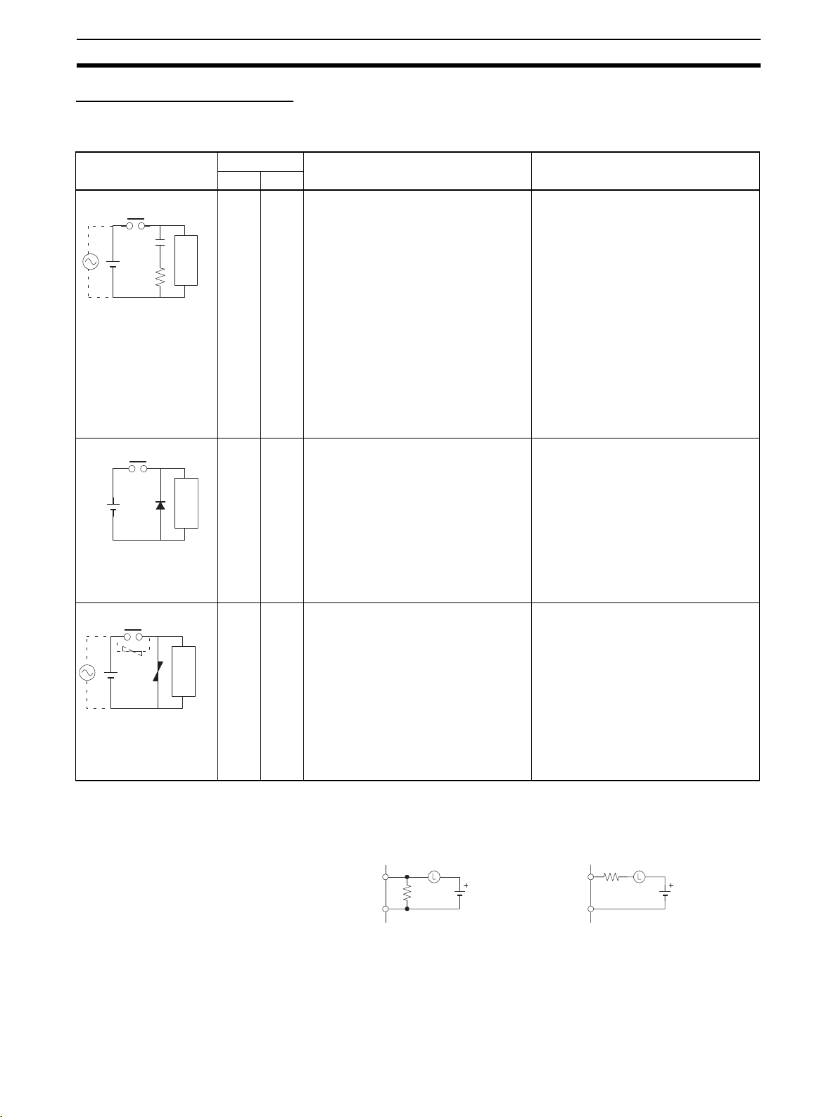
When switching an inductive load, connect an surge protector, diodes, etc., in
parallel with the load or contact as shown below.
Circuit Current Characteristic Required element
AC DC
CR method
Power
supply
Diode method
Power
supply
Varistor method
Power
supply
Yes Yes If the load is a relay or solenoid, there
is a time lag between the moment the
circuit is opened and the moment the
load is reset.
If the supply voltage is 24 or 48 V,
Inductive
load
insert the surge protector in parallel
with the load. If the supply voltage is
100 to 200 V, insert the surge protector
between the contacts.
No Yes The diode connected in parallel with
the load changes energy accumulated
by the coil into a current, which then
flows into the coil so that the current
will be converted into Joule heat by the
Inductive
load
resistance of the inductive load.
This time lag, between the moment the
circuit is opened and the moment the
load is reset, caused by this method is
longer than that caused by the CR
method.
Yes Yes The varistor method prevents the impo-
sition of high voltage between the contacts by using the constant voltage
characteristic of the varistor. There is
time lag between the moment the cir-
Inductive
load
cuit is opened and the moment the load
is reset.
If the supply voltage is 24 or 48 V,
insert the varistor in parallel with the
load. If the supply voltage is 100 to
200 V, insert the varistor between the
contacts.
The capacitance of the capacitor must
be 1 to 0.5 µF per contact current of
1 A and resistance of the resistor must
be 0.5 to 1 Ω per contact voltage of 1 V.
These values, however, vary with the
load and the characteristics of the
relay. Decide these values from experiments, and take into consideration that
the capacitance suppresses spark discharge when the contacts are separated and the resistance limits the
current that flows into the load when
the circuit is closed again.
The dielectric strength of the capacitor
must be 200 to 300 V. If the circuit is an
AC circuit, use a capacitor with no
polarity.
The reversed dielectric strength value
of the diode must be at least 10 times
as large as the circuit voltage value.
The forward current of the diode must
be the same as or larger than the load
current.
The reversed dielectric strength value
of the diode may be two to three times
larger than the supply voltage if the
surge protector is applied to electronic
circuits with low circuit voltages.
---
xx
When switching a load with a high inrush current such as an incandescent
lamp, suppress the inrush current as shown below.
Countermeasure 1
OUT
R
COM
Providing a dark current of
approx. one-third of the rated
value through an incandescent
lamp
Countermeasure 2
R
OUT
COM
Providing a limiting resistor
Page 20

Features and System Configuration
This section describes the features and system configuration of an ID Sensor Unit.
1-1 Outline of Features and Functions . . . . . . . . . . . . . . . . . . . . . . . . . . . . . . . . . 2
1-2 System Configuration . . . . . . . . . . . . . . . . . . . . . . . . . . . . . . . . . . . . . . . . . . . 4
1-2-1 Basic System Configuration . . . . . . . . . . . . . . . . . . . . . . . . . . . . . . . 4
1-2-2 Mounting Restrictions . . . . . . . . . . . . . . . . . . . . . . . . . . . . . . . . . . . 5
1-2-3 Mounting Units. . . . . . . . . . . . . . . . . . . . . . . . . . . . . . . . . . . . . . . . . 6
1-2-4 Unit Handling Precautions . . . . . . . . . . . . . . . . . . . . . . . . . . . . . . . . 8
1-3 Functions by Application . . . . . . . . . . . . . . . . . . . . . . . . . . . . . . . . . . . . . . . . 8
SECTION 1
1
Page 21
Outline of Features and Functions Section 1-1
1-1 Outline of Features and Functions
SYSMAC CS-series ID Sensor Units
Single-head ID Sensor Unit
(CS1W-V600C11)
V600C11
RUN
ERP
ERC
ERH
T/R
NORM/ERR
TEST
ON
HEAD
Double-head ID Sensor Unit
(CS1W-V600C12)
V600C12
RUN
ERP
ERC
HEAD1
NORM/ERR
DC24V
INPUT
ERH
HEAD2
T/R
T/R
NORM/ERR
TEST
ON
HEAD1
HEAD2
+
-
These ID Sensor Units read and write data for V600-series Data Carriers for
SYSMAC CS-series PLCs. There are two models: a Single-head ID Sensor
Unit (CS1W-V600C11) and a Double-head ID Sensor Unit (CS1W-V600C12).
CS-series Units can be mounted to a CS-series CPU Rack or CS-series
Expansion Rack.
SYSMAC CJ-series ID Sensor Units
Single-head ID Sensor Unit
These ID Sensor Units read and write data for V600-series Data Carriers for
SYSMAC CJ-series PLCs. There are two models: a Single-head ID Sensor
Unit (CJ1W-V600C11) and a Double-head ID Sensor Unit (CJ1W-V600C12).
CJ-series Units can be connected in a CJ-series CPU Rack or CJ-series
Expansion Rack.
(CJ1W-V600C11)
V600C11
RUN ERC
ERP ERH
T/R NORM/ERR
TEST
ON
HEAD
Double-head ID Sensor Unit
(CJ1W-V600C12)
V600C12
RUN ERC
ERP ERH
HEAD1
HEAD2
HEAD1
HEAD2
T/R NORM/ERR
T/R NORM/ERR
TEST
ON
2
Page 22

Outline of Features and Functions Section 1-1
Applicable Products and Commands
CS1W-V600C11 CS1W-V600C12 CJ1W-V600C11 CJ1W-V600C12
R/W Head V600-series (V600-H@@)
Maximum
number of
connected
Heads
Applicable
Data
Carriers
Commands Read
1212
V600-series Data Carriers (V600-D@@R@@ or V600-D@@P@@)
Write
Bit Set
Bit Clear
Mask Bit Write
Calculation Write
Data Fill
Data Check
Number of Writes Control
Read
Write
Bit Set
Bit Clear
Mask Bit Write
Calculation Write
Data Fill
Data Check
Number of Writes Control
Copy
Read
Write
Bit Set
Bit Clear
Mask Bit Write
Calculation Write
Data Fill
Data Check
Number of Writes Control
Read
Write
Bit Set
Bit Clear
Mask Bit Write
Calculation Write
Data Fill
Data Check
Number of Writes Control
Copy
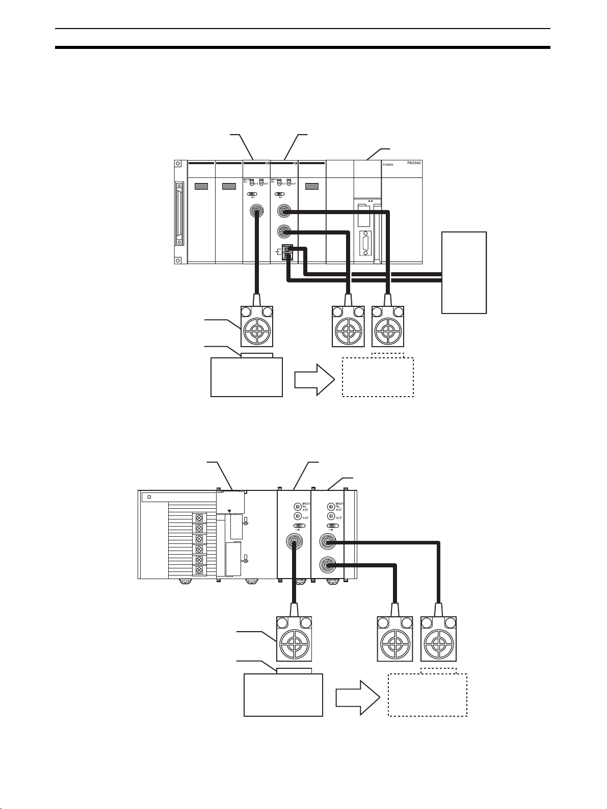
An RFID system consists of an ID Sensor Unit in a CS-series/CJ-series CPU
Rack or CS-series/CJ-series Expansion Rack, a R/W Head(s) connected to
the ID Sensor Unit, and Data Carriers connected to moving bodies.
The ID Sensor Unit operates through the R/W Head(s) to write data from the
CS/CJ-series CPU Unit to the Data Carriers and read data from the Data Carriers to the CS/CJ-series CPU Unit.
3
Page 23
System Configuration Section 1-2
1-2 System Configuration
1-2-1 Basic System Configuration
CS-series PLCs
Single-head ID Sensor Unit
R/W Head
NORM/ERR
V600C11
V600C12
RUN
ERP
RUN
ERC
ERH
ERC
HEAD1
T/R
T/R
NORM/ERR
TEST
TEST
ON
ON
HEAD
DC24V
INPUT
+
-
Double-head ID Sensor Unit
ERP
ERH
HEAD2
T/R
NORM/ERR
HEAD1
HEAD2
CPU Unit
24 V DC
power
supply
CJ-series PLCs
Data Carrier
Workpiece
(moving body)
Moves
Workpiece
(moving body)
Note The above example uses one Single-head ID Sensor Unit (CS1W-V600C11)
and one Double-head ID Sensor Unit (CS1W-V600C12).
CPU Unit Single-head ID Sensor Unit
Double-head ID Sensor Unit
SYSMAC
CJ1G-CPU44
PROGRAMMABLE
CONTROLLER
MCPWR
BUSY
R/W Head
OPEN
ERR/ALM
PERIHERAL
PORT
RUN
INH
PRPHL
COMM
V600C11
RUN ERC
ERP ERH
V600C12
T/R NORM/ERR
RUN ERC
T/R NORM/ERR
HEAD1
HEAD2
T/R NORM/ERR
ERP ERH
TEST
HEAD
TEST
ON
ON
HEAD1
HEAD2
Data Carrier
Workpiece
(moving body)
Moves
Workpiece
(moving body)
4
Page 24

System Configuration Section 1-2
Note The above example uses one Single-head ID Sensor Unit (CJ1W-V600C11)
and one Double-head ID Sensor Unit (CJ1W-V600C12).
1-2-2 Mounting Restrictions
CS-series PLCs CS-series ID Sensor Units are classified as CS-series Special I/O Units.
• These Units can be mounted to a CS-series CPU Rack or CS-series
Expansion Rack.
• The number of Units per CPU Rack or Expansion Rack depends on the
maximum supply current of the Power Supply Unit and current consumption of other Units on the Rack.
The following table lists the maximum number of Units per Rack when only ID
Sensor Units are mounted.
Power Supply Unit CS1W-V600C11 CS1W-V600C12
C200HW-PA204
C200HW-PA204S
C200HW-PA204R
C200HW-PD204
C200HW-PA209R
CJ-series PLCs CJ-series ID Sensor Units are classified as CJ-series Special I/O Units.
• These Units can be mounted to a CJ-series CPU Rack or CJ-series
Expansion Rack.
• The number of Units per CPU Rack or Expansion Rack depends on the
maximum supply current of the Power Supply Unit and current consumption of other Units on the Rack.
The following table lists the maximum number of Units per Rack when only ID
Sensor Units are mounted.
Power Supply Unit CJ1W-V600C11 CJ1W-V600C12
CJ1W-PA205R 4 2
CJ1W-PA202 2 1
510
Note The I/O words allocated to Special I/O Units are determined by the setting of
the unit number switches on the front of the Unit. They are not affected by the
slots (positions) in which the Units are mounted.
5
Page 25
System Configuration Section 1-2
1-2-3 Mounting Units
CS-series PLCs Use the following procedure to mount an ID Sensor Unit to the Backplane.
1,2,3... 1. Lock the top of the ID Sensor Unit into the slot on the Backplane and rotate
the Unit downwards as shown in the following diagram.
Hook
Backplane
2. While making sure to align the Unit properly with the connectors, tighten
the mounting screws securely to a tightening torque of 0.4 N·m.
3. To remove the Unit, first loosen the mounting screws using a Phillips
screwdriver.
Mounting screw
Note Leave enough space below each Rack, as shown in the following diagram, for
mounting and removing the Units.
20 mm min.
Backplane
20 mm min.
Phillips screwdriver
6
Page 26
System Configuration Section 1-2
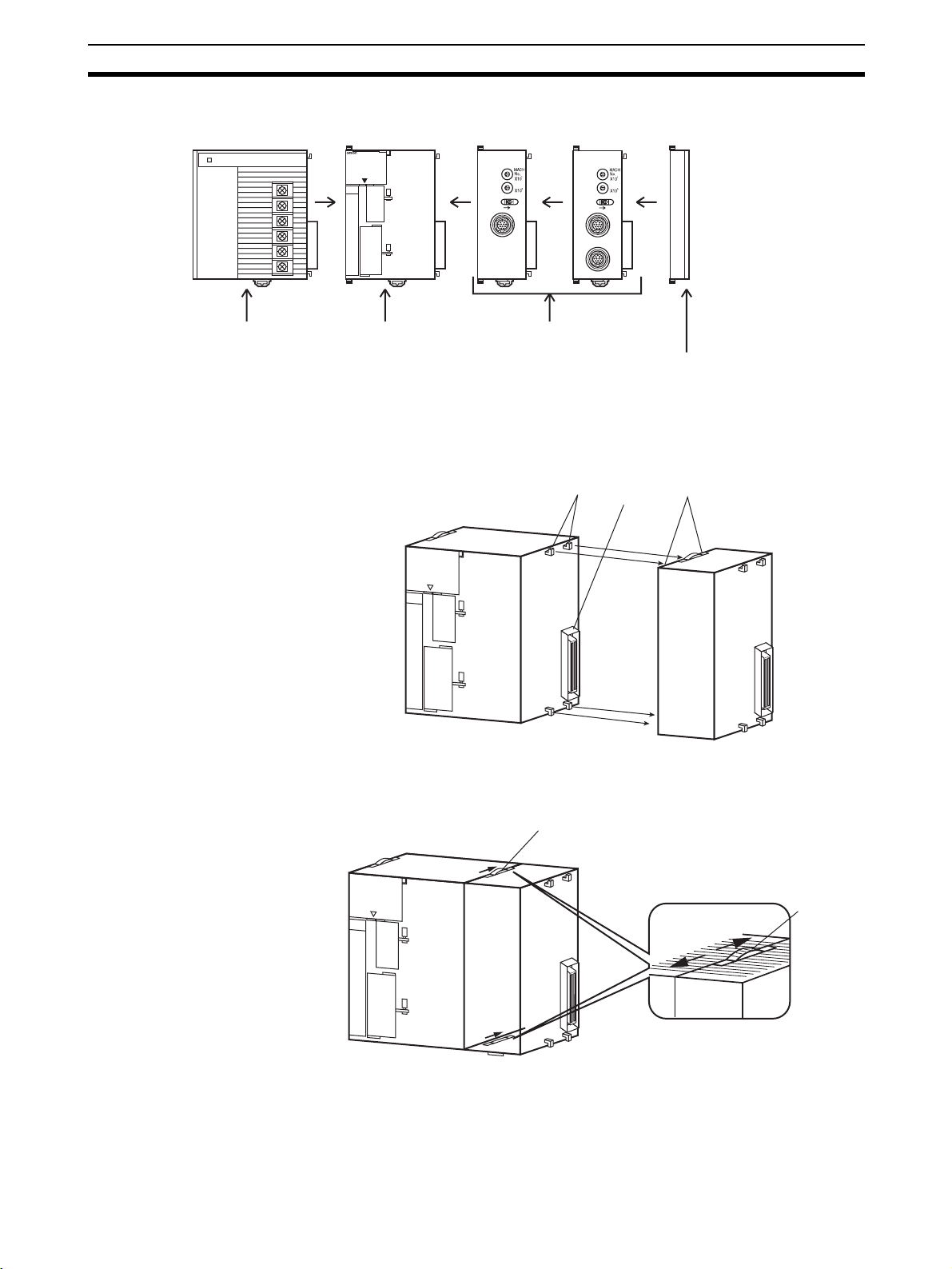
CJ-series PLCs ID Sensor Units are connected as I/O Units in the system configuration, as
shown below.
SYSMAC
CJ1G-CPU44
PROGRAMMABLE
CONTROLLER
RUN
ERR/ALM
INH
PRPHL
COMM
OPEN
MCPWR
BUSY
PERIHERAL
V600C11
RUN ERC
T/R NORM/ERR
ERP ERH
TEST
ON
HEAD
V600C12
RUN ERC
T/R NORM/ERR
HEAD1
HEAD2
T/R NORM/ERR
ERP ERH
TEST
ON
HEAD1
HEAD2
Power Supply Unit
PORT
CPU Unit I/O Units
(10 Units max.)
End Cover
(included with CPU Unit)
Use the following procedure to connect an ID Sensor Unit.
1,2,3... 1. Align the connectors and press in firmly on the Units to connect them com-
pletely.
Hooks
Connector
Hook holes
2. Move the yellow sliders on the top and bottom of the Unit to the lock position to secure the Units. The sliders should click into place.
Move the sliders to the back
until they click into place.
Slider
Locked
Released
3. Attach an End Cover to the Unit on the right end of the Rack.
Note The CJ-series PC may not operate properly if the sliders are not locked firmly
into place.
7
Page 27
Functions by Application Section 1-3
1-2-4 Unit Handling Precautions
Be sure to turn OFF the power supply to the PLC before installing or disconnecting Units, or connecting lines.
To reduce the risk of malfunctioning due to electrical noise, wire input and output lines in separate ducts from high-voltage and power lines.
When wiring a Unit, leave the label in place on the top of the Unit to prevent
wire clippings or other materials from getting inside the Unit. When wiring has
been completed, remove the label to ensure proper heat dissipation.
CS-series PLCs
Remove the label after
wiring has been completed.
CJ-series PLCs
Remove the label after
wiring has been completed.
1-3 Functions by Application
Application Function Reference
Performing communications test with Data Carriers without programming
the CPU Unit
Adjusting communications timing with Data Carriers
Examples:
Communicating with Data Carriers stopped in front of the R/W Head
Communicating with Data Carriers passing by the R/W Head
Protecting Data Carrier memory once it has been written Write protection Page 61
Managing Data Carrier life Data Carrier life check Page 64
Checking the suitability of Data Carrier memory Data check Page 69
Communications test mode Page 52
Communications specifications Page 52
8
Page 28

SECTION 2
CS-series ID Sensor Units
This section describes the specifications, operation, and installation of ID Sensor Units for CS-series PLCs.
2-1 Specifications . . . . . . . . . . . . . . . . . . . . . . . . . . . . . . . . . . . . . . . . . . . . . . . . . 10
2-1-1 General Specifications . . . . . . . . . . . . . . . . . . . . . . . . . . . . . . . . . . . 10
2-1-2 Performance Specifications . . . . . . . . . . . . . . . . . . . . . . . . . . . . . . . 10
2-1-3 Communications Specifications . . . . . . . . . . . . . . . . . . . . . . . . . . . . 11
2-2 Operating Procedure . . . . . . . . . . . . . . . . . . . . . . . . . . . . . . . . . . . . . . . . . . . . 12
2-2-1 Overall Procedure . . . . . . . . . . . . . . . . . . . . . . . . . . . . . . . . . . . . . . . 12
2-2-2 Operating Procedure Example . . . . . . . . . . . . . . . . . . . . . . . . . . . . . 13
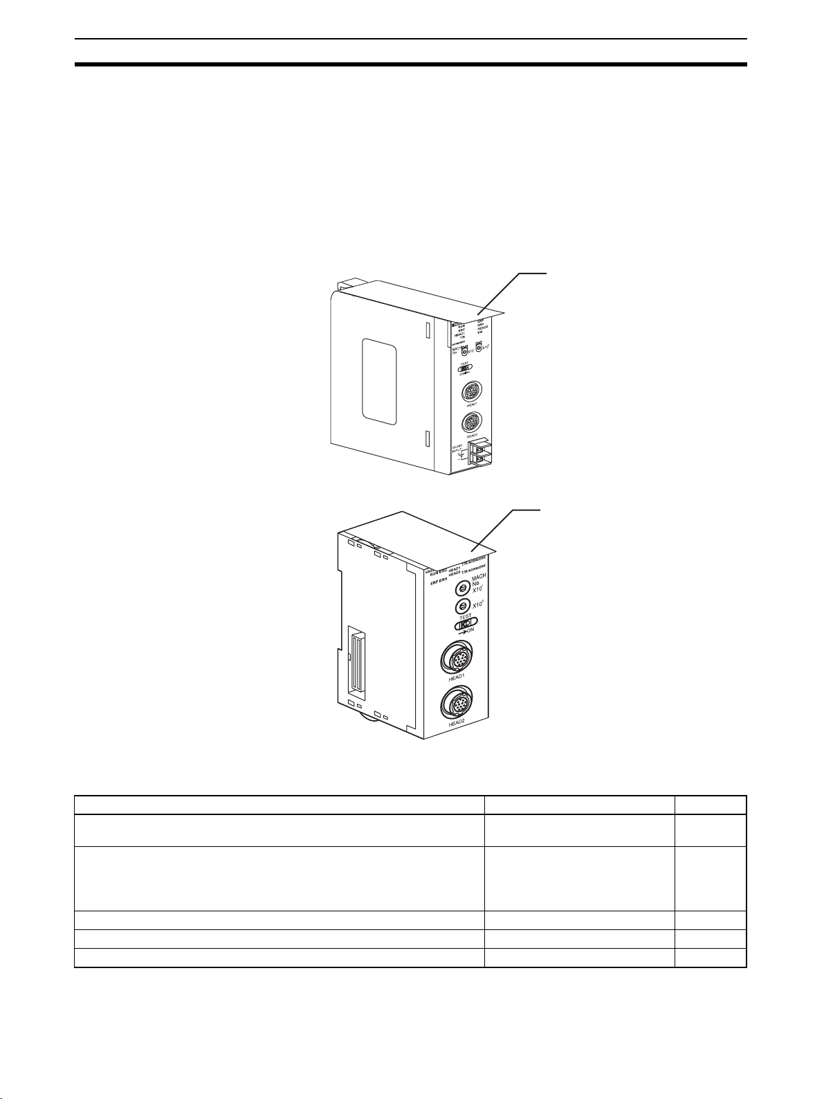
2-3 Part Names and Functions. . . . . . . . . . . . . . . . . . . . . . . . . . . . . . . . . . . . . . . . 17
2-3-1 Part Names . . . . . . . . . . . . . . . . . . . . . . . . . . . . . . . . . . . . . . . . . . . . 17
2-3-2 Indicators . . . . . . . . . . . . . . . . . . . . . . . . . . . . . . . . . . . . . . . . . . . . . 18
2-3-3 Unit Number Switches . . . . . . . . . . . . . . . . . . . . . . . . . . . . . . . . . . . 18
2-3-4 Communications Test Switch . . . . . . . . . . . . . . . . . . . . . . . . . . . . . . 18
2-4 Connections and Wiring . . . . . . . . . . . . . . . . . . . . . . . . . . . . . . . . . . . . . . . . . 19
2-4-1 Connecting R/W Heads . . . . . . . . . . . . . . . . . . . . . . . . . . . . . . . . . . 19
2-4-2 Wiring the External Power Supply (CS1W-V600C12 Only) . . . . . . 20
2-4-3 Wiring for Safety and Noise Immunity . . . . . . . . . . . . . . . . . . . . . . 21
9
Page 29

Specifications Section 2-1
2-1 Specifications
2-1-1 General Specifications
General specifications conform to those of SYSMAC CS-series Special I/O
Units.
2-1-2 Performance Specifications
CS1W-V600C11 CS1W-V600C12
Unit classification
Influence on
CPU Unit’s cycle
time
Input power supply
Internal current
consumption
Dimensions 35 × 130 × 101 mm (W×H×D)
Weight 180 g max. 300 g max.
Mounting loca-
tion
No. of Units per
Rack
Connectable
Heads
Applicable Data
Carriers
No. of allocated
unit numbers
No. of allocated
words
Control protocol Special protocol
Data exchange
methods with
CPU Unit
Data transfer
quantity
Operating
modes
Diagnostic functions
Special I/O Unit
0.15 ms 0.3 ms
--- 24 V DC +10%/−15%, 360 mA
5 V DC, 260 mA max.; 26 V DC, 120 mA max. 5 V DC, 320 mA max.; 26 V DC, 0 mA max.
CS-series CPU Rack or CS-series Expansion Rack
(Cannot be mounted to C200H Expansion I/O Racks or SYSMAC BUS Slave Racks.)
5 per Rack (CPU Rack or Expansion Rack) 10 per Rack (CPU Rack or Expansion Rack)
V600-series R/W Heads
(V600-H@@) 1 Head
V600-series Data Carriers (V600-D@@)
12
10 words 20 words
Special I/O Unit Area in
CIO Area
CIO 2000 to CIO 2959
Special I/O Unit words
in DM Area
D20000 to D29599
2,048 bytes max.
(160 bytes/scan)
Normal Mode/Test Mode (changed with communications test switch)
(1) ID Sensor Unit error
(2) Communications error detection with Data Carriers
(3) Head 24-V power supply error
Constant data exchange
of 10 words/Unit
100 words/Unit transferred when power is
turned ON or when
restarting the Unit
V600-series R/W Heads
(V600-H@@) 1 or 2 Heads
CPU Unit
→ ID Sensor Unit
ID Sensor Unit
→ CPU Unit
CPU Unit
→ ID Sensor Unit
2,048 bytes max./Head
(160 bytes/scan)
Unit Controls, Communications Processing
specification, Data storage area specification
Unit information,
Results information
Processing results monitor
System Settings
Auto Wait Time Setting
10
Page 30

Specifications Section 2-1
2-1-3 Communications Specifications
CS1W-V600C11 CS1W-V600C12
Communications frequency 530 kHz
Communications controls (1) Changing EEPROM (battery-free) Data Carrier communications mode (distance prior-
ity or time priority)
(2) Write verification
(3) Auto Wait Time Setting
Commands Read
Write
Bit Set/Bit Clear
Mask Bit Write
Calculation Write
Data Fill
Data Check
Number of Writes Control
Communications specification Trigger, Single auto, Repeat auto
Read
Write
Bit Set/Bit Clear
Mask Bit Write
Calculation Write
Data Fill
Data Check
Number of Writes Control
Copy
11
Page 31

Operating Procedure Section 2-2
2-2 Operating Procedure
2-2-1 Overall Procedure
The operating procedure for an ID Sensor Unit is shown in the following flowchart.
Installation and settingsTrail operationOperation
Set switch on front of Unit
Wire
Set unit number
Turn ON PLC power
Create I/O tables
Set words allocated in DM Area
Turn PLC power OFF and ON
Set switch on front of Unit
Test communications
Change DIP switch on front of Unit
Turn OFF the communications test switch.
Set unit number switches on front of Unit.
Set communications mode.
Enable/disable verification when writing.
Set auto wait time
OR, turn ON Special I/O Unit Restart Bit.
Turn ON the communications test switch.
Place PLC in PROGRAM mode.
12
Turn ON PLC power
Ladder program operation
OR, turn ON Special I/O Unit Restart Bit.
Note 1. When using CX-Programmer V3.0 or later with the CS1W-V600C12, “I” will
be displayed before addresses for inputs in the ladder diagram and “Q” will
be displayed before addresses for outputs for operation data. In the CXProgrammer’s I/O Table Window, select SIOU/C200H ASCII Unit (A) and
then, from the Enter SIOU Details Window, set the Address per Unit to 2,
the Input Words to 3, and the Output Words to 7, and select the Repeat IN/
OUT for each Address per Unit option.
2. When using CX-Programmer V2.0 or later with the CS1W-V600C11, “I” will
be displayed in the ladder diagram before address for inputs and “Q” will
be displayed before addresses for outputs for operation data.
Page 32

Operating Procedure Section 2-2
2-2-2 Operating Procedure Example
The following is an operating procedure example for the following conditions.
Reading 10 Bytes of Data from Data Carrier Address 0010 Using a Trigger
ID Sensor Unit Settings
1,2,3... 1. Communications Test Switch (Set on Unit’s front panel.)
CS-series CPU Unit
Special I/O
Unit Area
Bit
15
D1000 01 02
D1001 03 04
D1002
D1003
D1004
→: Read data storage order
05 06
07 08
09 0A
Read command
Bit
00
Read data
Special I/O Unit Area Settings
Unit No.: 00
Command: Read
Communications specification: Trigger
Read data storage order: Leftmost
→ Rightmost
First Data Carrier read address: 0010 (hex)
Number of Data Carrier read bytes: 10 bytes
Read data storage destination: D1000 to D1004
CS1W-V600C11
V600C11
RUN
ERP
ERC
ERH
T/R
NORM/ERR
TEST
ON
HEAD
Communications
Data Carrier
Bit
Address
7
(hex)
0010 0 1
0011 0 2
0012 0 3
0013 0 4
0014 0 5
0015 0 6
0016 0 7
0017 0 8
0018 0 9
0019 0 A
Bit
0
2. Mounting and Installation
TEST
ON
Communications test switch
13
Page 33

Operating Procedure Section 2-2
3. Unit No. Setting
0
9
1
8
2
7
3
6
4
5
0
9
1
8
2
7
3
6
4
5
Set the unit number to 0, and the
following words will be allocated
to the Unit as a Special I/O Unit.
• CIO Area: CIO 2000 to CIO 2009
• DM Area: D20000 to D20099
4. PLC Power Supply ON
Power supply ON
Creating I/O Tables Always create the I/O tables after turning ON the PLC power supply. The I/O
tables can be created from the Programming Console or CX-Programmer.
Peripheral port
Programming Console
14
Page 34

Operating Procedure Section 2-2
Initial Settings
1,2,3... 1. Make the settings in the words allocated to Special I/O Units in the DM
Area (refer to page 41).
Peripheral port
Programming Console
First word allocated to Unit in DM Area: m = D20000 + (100
DM
address
D20000 0000Not used Communications
D20001 0000 Auto Wait Time Setting: Infinite
Contents Meaning
1514131211109876543210
test switch enabled
2. PLC Power Supply OFF and ON (or turn ON the Unit Restart Bit)
Ladder Programming
Verification for writing
Peripheral port
× 0) = D20000
Communications
mode: Distance
Programming Console
Set the Command, Communications Specification, Read Data Storage Order, First Data Carrier Read Address, Number of Bytes to Read, and Read
Data Storage Destination in words (n + 1) to (n + 6) allocated in the Special
I/O Unit Area (here, CIO 2001 to CIO 2006).
15
Page 35

Operating Procedure Section 2-2
First word allocated to Unit in CIO Area: CIO 2000 + 10 × 0 = CIO 2000
Word
address
CIO 2001 00 0 0 Command Communications
Contents Meaning
1514131211109876543210
Data order
specification
CIO 2002 00 10 First read address
CIO 2003 00 0A Number of read bytes
CIO 2004 10 00 Read data storage location (rightmost 4 digits)
CIO 2005 0 0 00 Data storage area Bank designation* Read data storage location (leftmost 2
digits)
CIO 2006 00 00 ---
Note *: Always 0 when DM is specified. ---: Ignored.
Execution
input
Waiting for
command
execution
(work bit)
0010.01
ID Busy
2007.00
Test Mode
2007.14
Unit Busy
2007.15
MOV
#0000
2001
MOV
#0010
2002
MOV
#000A
2003
Specification of command,
communications specification,
and read data storage order.
Specification of first read address.
Specification of number of read bytes.
Waiting for command
execution (work bit)
0010.01
Abort input
Waiting for abort
(work bit)
0010.02
Normal End Flag
2007.01
Error End Flag
2007.02
ID
Busy
2007.00
MOVL
#00001000
2004
0010.01
2000.00
2000.02
0010.02
Read data storage location
Waiting for command execution
(work bit)
Command Execution Bit
Abort Bit
Waiting for Abort
(work bit)
Normal end
Used to time getting
read data.
Error end
Used to time getting
resulting information.
16
Page 36

Part Names and Functions Section 2-3
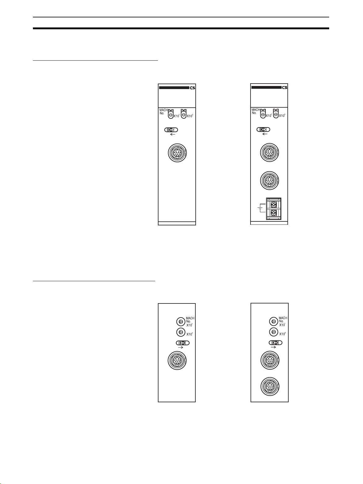
2-3 Part Names and Functions
2-3-1 Part Names
CS1W-V600C11 CS1W-V600C12
V600C11
RUN
ERC
NORM/ERR
(front)
T/R
ERP
ERH
V600C12
RUN
ERC
HEAD1
NORM/ERR
(front)
T/R
ERP
ERH
HEAD2
T/R
NORM/ERR
Status indicators
Unit number switches
ON
TEST
Communications test switch
TEST
ON
R/W Head connector
HEAD
DC24V
INPUT
HEAD1
HEAD2
+
-
R/W Head power terminals
(Back) (Side)
Backplane
connector
Terminal
block
17
Page 37

Part Names and Functions Section 2-3
2-3-2 Indicators
Indicators show the operating status of the Unit. The relationship between the
indicator status and the Unit status is shown in the following table.
Indicator Name Color Meaning
RUN RUN Green Lit The ID Sensor Unit is operating normally.
Not lit The ID Sensor Unit is stopped.
ERC
(Error I/O Controller)
ERH
(Error at Host)
ERP
(Head Power Error)
Head 1 T/R Communicating Yellow Lit Communications are active.
NORM/ERR Normal end Green Lit Communications with the Data Carrier ended
Head 2 T/R Communicating Yellow Lit Communications are active.
NORM/ERR Normal end Green Lit Communications with the Data Carrier ended
Unit error Red Lit An error has occurred in the ID Sensor Unit.
Not lit No error has occurred in the ID Sensor Unit.
CPU Unit error Red Lit An error has occurred in the CPU Unit.
Not lit No error has occurred in the CPU Unit.
Head power error Red Lit An error has occurred in the power supply to the
R/W Head.
Not lit The power supply to the R/W Head is normal.
normally.
Error end Red Lit Communications with the Data Carrier ended in
an error.
normally.
Error end Red Lit Communications with the Data Carrier ended in
an error.
2-3-3 Unit Number Switches
Data exchange between the CPU Unit and ID Sensor Unit is performed using
words allocated to the Unit in the Special I/O Unit Area and in the DM Area.
The words allocated to the ID Sensor Unit in these two areas are determined
by the setting of the unit number switches on the Unit’s front panel.
0
9
1
8
2
7
3
6
4
5
0
9
1
8
2
7
3
6
4
5
Switch
No.
Unit
No.
allocated in
Special I/O
Unit Area
0 Unit 0 CIO 2000 to
CIO 2009
1 Unit 1 CIO 2010 to
CIO 2019
::: : : :
94 Unit 94 CIO 2940 to
CIO 2949
95 Unit 95 CIO 2950 to
CIO 2959
2-3-4 Communications Test Switch
The communications test switch on the Unit’s front panel is used to switch
between Normal Mode and Test Mode.
TEST
ON
Status Description
OFF Normal status (factory setting)
ON Communications test
CS1W-V600C11 CS1W-V600C12
Words
Words
allocated in
DM Area
Words
allocated in
Special I/O
Unit Area
D20000 to
D20099
D20100 to
D20199
D29400 to
D29499
D29500 to
CIO 2000 to
CIO 2019
CIO 2010 to
CIO 2029
CIO 2940 to
CIO 2959
(Cannot be set)
D29599
Words
allocated in
DM Area
D20000 to
D20199
D20100 to
D20299
D29400 to
D29599
18
Page 38

Connections and Wiring Section 2-4
2-4 Connections and Wiring
2-4-1 Connecting R/W Heads
Connection Method
1,2,3... 1. Holding the rubber molding on the connector, align the connector with the
key groove and press in.
2. Press in on the connector until it locks in place.
Rubber molding
Ring
Note The connector will not lock into place if you hold onto the ring. Always hold
onto the rubber molding.
Removal Method Hold onto the ring and pull straight out.
Rubber molding
Ring
Note The connector cannot be removed if you hold onto the rubber molding. Never
pull on the cable with excessive force. The conductors may be broken or damaged.
19
Page 39

Connections and Wiring Section 2-4
2-4-2 Wiring the External Power Supply (CS1W-V600C12 Only)
Wiring the power supply as shown below.
CS1W-V600C12
Connection Example
Line filter
+24 V DC
0 V
M3 self-lifting screws are used as the connection terminals for the power supply. When necessary, use the following crimp terminals. The tightening torque
is approximately 0.59 N·m.
Examples of Applicable Crimp Connectors
Manufacturer Model number Applicable wire size Shape
J.S.T Mfg. Co., Ltd. 1.25-N3A AWG24 to 16 Forked
J.S.T Mfg. Co., Ltd. 1.25-Y3A
6.5 mm max.
Recommended DC Power Supplies (Miniature, by OMRON)
Model number Output capacity Input voltage
S82K-03024 24 V DC, 1.3 A 100/200 V AC
S82J-0224 24 V DC, 1.1 A 100 V AC
Note 1. Although adequate measures have been taken inside the I/O Sensor Unit
for noise entering on the power supply line, supplying power through a line
filter can be used to greatly attenuate ground noise.
2. Although the rated power consumption of the CS1W-V600C12 is 360 mA
at 24 V DC, be sure to consider the surge current when determining capacities.
(For M3 terminal)
20
Page 40

Connections and Wiring Section 2-4
2-4-3 Wiring for Safety and Noise Immunity
R/W Head Cables and I/O
Signal Lines
Countermeasures for
Inductive Loads
Wire the R/W Head cables and I/O signal lines in separate ducts from power
circuit cables both inside and outside the control panel.
(1): I/O cables
(2): Power lines
(1)
(2)
Suspended ducts
(1) (2)
Floor ducts
(1) (2)
Conduits
If the same ducts must be used, shielded cables can be used to increase
resistance to noise. If a shielded cable is used, connect one end of the shield
to ground.
If I/O is connected to an inductive load, connect a surge killer or diode in parallel with the load.
IN
Diode
L
DC input
COM
Relay contact output
Triac output
OUT
COM
L
Surge killer
Noise Countermeasures
for External Wiring
OUT
Relay contact output
Transistor output
COM
Diode
Note Use surge killers and diodes that meet the following conditions:
Surge Killers
Resistance: 50 Ω
Capacitance: 0.47 µF
Voltage: 200 V
Diodes
Inrush withstand voltage: 3 times load voltage min.
Average rectified current: 1 A
Consider the following items when wiring external lines, such as the R/W
Head cables, I/O lines, power supply lines, and high-power lines.
• When using multiconductor cables for signal lines, do not use the same
cable for both I/O lines and other control lines.
+
21
Page 41

Connections and Wiring Section 2-4
• When Racks are installed in parallel with each other, keep them separated by at least 300 mm.
Low-power cables
R/W Head cables and
PLC I/O lines
Control cables
SYSMAC power supply
lines and general
control circuit lines
Power lines
High-power cables
Ground to 100 Ω or less.
• When placing cables in the same duct, separate them with grounded iron
plates.
SYSMAC power supply
lines and general
control circuit lines
Power linesPLC I/O lines
300 mm min.
300 mm min.
Iron plate
200 mm min.
Ground to 100 Ω or less.
22
Page 42

SECTION 3
CJ-series ID Sensor Units
This section describes the specifications, operation, and installation of ID Sensor Units for CJ-series PLCs.
3-1 Specifications . . . . . . . . . . . . . . . . . . . . . . . . . . . . . . . . . . . . . . . . . . . . . . . . . 24
3-1-1 General Specifications . . . . . . . . . . . . . . . . . . . . . . . . . . . . . . . . . . . 24
3-1-2 Performance Specifications . . . . . . . . . . . . . . . . . . . . . . . . . . . . . . . 24
3-1-3 Communications Function Specifications . . . . . . . . . . . . . . . . . . . . 25
3-2 Operating Procedure . . . . . . . . . . . . . . . . . . . . . . . . . . . . . . . . . . . . . . . . . . . . 26
3-2-1 Overall Procedure . . . . . . . . . . . . . . . . . . . . . . . . . . . . . . . . . . . . . . . 26
3-2-2 Operating Procedure Example . . . . . . . . . . . . . . . . . . . . . . . . . . . . . 27
3-3 Part Names and Functions. . . . . . . . . . . . . . . . . . . . . . . . . . . . . . . . . . . . . . . . 31
3-3-1 Part Names . . . . . . . . . . . . . . . . . . . . . . . . . . . . . . . . . . . . . . . . . . . . 31
3-3-2 Indicators . . . . . . . . . . . . . . . . . . . . . . . . . . . . . . . . . . . . . . . . . . . . . 32
3-3-3 Unit Number Switches . . . . . . . . . . . . . . . . . . . . . . . . . . . . . . . . . . . 32
3-3-4 Communications test Switch . . . . . . . . . . . . . . . . . . . . . . . . . . . . . . 32
3-4 Connections and Wiring . . . . . . . . . . . . . . . . . . . . . . . . . . . . . . . . . . . . . . . . . 33
3-4-1 Connecting R/W Heads . . . . . . . . . . . . . . . . . . . . . . . . . . . . . . . . . . 33
3-4-2 Wiring for Safety and Noise Immunity . . . . . . . . . . . . . . . . . . . . . . 34
23
Page 43

Specifications Section 3-1
3-1 Specifications
3-1-1 General Specifications
General specifications conform to those of SYSMAC CJ-series Special I/O
Units.
3-1-2 Performance Specifications
CJ1W-V600C11 CJ1W-V600C12
Unit classification
Influence on
CPU Unit’s cycle
time
Internal current
consumption
Dimensions 31 × 90 × 65 mm (W×H×D)
Weight 120 g max. 130 g max.
Mounting loca-
tion
No. of Units per
Rack
Connectable
Heads
Applicable Data
Carriers
No. of allocated
unit numbers
No. of allocated
words
Control protocol Special protocol
Data exchange
methods with
CPU Unit
Data transfer
quantity
Operating
modes
Diagnostic functions
Special I/O Unit
0.15 ms 0.3 ms
5 V DC, 260 mA max.; 24 V DC, 120 mA max. 5 V DC, 320 mA max.; 24 V DC, 240 mA max.
CJ-series Rack or CJ-series Expansion Rack
(Cannot be mounted to C200H Expansion I/O Racks or SYSMAC BUS Slave Racks.)
4 Units maximum per Rack 2 Units maximum per Rack
V600-series R/W Heads
(V600-H@@) 1 Head
V600-series Data Carriers (V600-D@@)
1 unit number 2 unit numbers
10 words 20 words
Special I/O Unit Area
CIO 2000 to CIO 2959
Special I/O Unit words
in DM Area
D20000 to D29599
2,048 bytes max.
(160 bytes/scan)
Normal Mode/Test Mode (changed with communications test switch)
(1) ID Sensor Unit error
(2) Communications error detection with Data Carriers
(3) Head 24-V power supply error
Constant data exchange
of 10 words/Unit
100 words/Unit transferred when power is
turned ON or when
restarting the Unit
V600-series R/W Heads
(V600-H@@) 1 or 2 Heads
CPU Unit
→ ID Sensor Unit
ID Sensor Unit
→ CPU Unit
CPU Unit
→ ID Sensor Unit
2,048 bytes max./Head
(160 bytes/scan)
Unit Controls, Communications Processing
Specification, Data Storage Area Specification
Unit information,
Results Information,
Processing Results
Monitor
System Settings,
Auto Wait Time Setting
24
Page 44

Specifications Section 3-1
3-1-3 Communications Function Specifications
CJ1W-V600C11 CJ1W-V600C12
Communications frequency 530 kHz
Communications control (1) Changing EEPROM (battery-free) Data Carrier communications mode (distance prior-
ity or time priority)
(2) Write verification
(3) Auto Wait Time Setting
Commands Read
Write
Bit Set/Bit Clear
Mask Bit Write
Calculation Write
Data Fill
Data Check
Number of Writes Control
Communications specification Trigger, Single auto, Repeat auto
Read
Write
Bit Set/Bit Clear
Mask Bit Write
Calculation Write
Data Fill
Data Check
Number of Writes Control
Copy
25
Page 45

Operating Procedure Section 3-2
3-2 Operating Procedure
3-2-1 Overall Procedure
The operating procedure for an ID Sensor Unit is shown in the following flowchart.
Set switch on front of Unit
Set unit number
Turn ON PLC power
Create I/O tables
Installation and settings
Set words allocated in DM Area
Turn PLC power OFF and ON.
Set switch on front of Unit
Test communications
Trail operationOperation
Change DIP switch on front of Unit
Turn OFF the communications test switch.
Wire
Set unit number switches on front of Unit.
Set communications mode.
Enable/disable verification when writing.
Set auto wait time
OR, turn ON Special I/O Unit Restart Bit.
Turn ON the communications test switch.
Place PLC in PROGRAM mode.
26
Turn ON PLC power
Ladder program operation
OR, turn ON Special I/O Unit Restart Bit.
Note 1. When using CX-Programmer V3.0 or later with the CJ1W-V600C12, “I” will
be displayed before addresses for inputs in the ladder diagram and “Q” will
be displayed before addresses for outputs for operation data. In the CXProgrammer’s I/O Table Window, select SIOU/C200H ASCII Unit (A) and
then, from the Enter SIOU Details Window, set the Address per Unit to 2,
the Input Words to 3, and the Output Words to 7, and select the Repeat IN/
OUT for each Address per Unit option.
2. When using CX-Programmer V2.0 or later with the CJ1W-V600C11, “I” will
be displayed in the ladder diagram before address for inputs and “Q” will
be displayed before addresses for outputs for operation data.
Page 46

Operating Procedure Section 3-2
3-2-2 Operating Procedure Example
The following is an operating procedure example for the following conditions.
Reading 10 Bytes of Data from Data Carrier Address 0010 Using a Trigger
ID Sensor Unit Settings
1,2,3... 1. Communications Test Switch (Set on Unit’s front panel.)
CJ-series CPU Unit
Special I/O
Unit Area
Bit
15 00
Read command
Bit
D1000 01 02
D1001 03 04
D1002
D1003
D1004
05 06
07 08
09 0A
Read data
→: Read data storage order
Special I/O Unit Area Settings
Unit No.: 00
Command: Read
Communications specification: Trigger
Read data storage order: Leftmost
→ Rightmost
First Data Carrier read address: 0010 (hex)
Number of Data Carrier read bytes: 10 bytes
Read data storage destination: D1000 to D1004
CJ1W-V600C11
V600C11
RUN ERC
T/R NORM/ERR
ERP ERH
TEST
ON
HEAD
Address
Communications
Data Carrier
Bit
70
(hex)
0010 0 1
0011 0 2
0012 0 3
0013 0 4
0014 0 5
0015 0 6
0016 0 7
0017 0 8
0018 0 9
0019 0 A
Bit
NORM/ERR
R
/
T
1
1
C
0
0
6
V
C
R
E
N
U
R
H
R
E
P
R
E
T
S
E
T
N
O
2. Mounting and Installation
TEST
ON
M
S
Y
S
CJ1G
PROG
ROL
T
N
CO
Communications test switch
/ERR
NORM
T/R
1
1
C
0
V60
N ERC
RU
7
6
5
14 15
34
1
2
6
2
D
15
01
O
ERP ERH
4
910111213
13 1
8
234567
12
I
01
2
91011
8
I
I
3
0
RUN
ALM
/
R
R
E
NH
I
C
A
4
4
U
P
E
C
PRPHL
L
-
B
A
M
M
M
COM
RA
R
E
L
EN
P
O
R
W
MCP
Y
BUS
AL
R
IHE
R
PE
T
R
PO
I
1
I
I
1
20
CN1
3A
0.
V
DC24
1
B/A
TEST
ON
CN2
20
A/B
27
Page 47

Operating Procedure Section 3-2
3. Unit No. Setting
7
8
1
6
2
123
D
0
O
891011 1
I
01
9
8
I
I
0
2
1
N
C
DC24V 0.3A
1
/A A
B
6
9
5
0
4
1
3
2
7
8
6
9
5
0
4
1
3
2
M/ERR
NOR
T/R
1
1
C
0
0
6
V
RUN ERC
7
56
15
4
7
21314
56
5
1
ERP ERH
4
13 14
23
2
1
11
10
2
3
0
I
1
I
I
1
T
S
E
T
N
O
2
N
C
0
2
/B
4. PLC Power Supply ON
NORM/ERR
T/R
1
1
C
0
0
6
V
C
R
E
N
U
R
H
R
E
P
ER
T
S
E
T
N
O
Set the unit number to 0, and the
following words will be allocated
to the Unit as a Special I/O Unit.
• CIO Area: CIO 2000 to CIO 2009
• DM Area: D20000 to D20099
N
U
R
M
L
A
/
R
R
E
H
N
I
C
A
M
4
S
L
4
Y
H
U
S
P
P
R
E
C
P
L
-
B
G
A
1
M
M
J
M
M
C
O
A
C
R
G
R
O
E
R
L
P
L
O
R
T
N
O
C
N
E
P
O
R
PW
MC
Y
S
U
B
L
A
R
E
IH
R
E
P
T
R
O
P
Creating I/O Tables Always create the I/O tables after turning ON the PLC power supply. The I/O
tables can be created from the Programming Console or CX-Programmer.
Peripheral port
NORM/ERR
T/R
1
C1
0
V60
RUN ERC
7
56
15
13 14
7
1
H
6
12
2
1234
D
15
0
O
ERP ER
10 11
456
14
9
3
3
1
8
2
2
1
I
1
0
2
91011
8
I
I
3
0
RUN
M
/AL
R
R
E
INH
C
A
M
4
S
L
4
Y
U
S
P
E
C
PRPH
L
-
B
A
M
M
M
CJ1G
OM
C
GRA
R
E
L
PRO
ROL
T
N
CO
PEN
O
MCPWR
Y
BUS
AL
R
IHE
R
PE
ORT
P
I
1
I
I
1
20
CN1
3A
0.
DC24V
1
/A
B
TEST
ON
CN2
20
A/B
Programming Console
28
Page 48

Operating Procedure Section 3-2
Initial Settings
1,2,3... 1. Make the settings in the words allocated to Special I/O Units in the DM
Area (refer to page 41).
Peripheral port
M/ERR
NOR
/R
T
1
C1
0
V60
RUN ERC
15
4567
13 14
7
1
23
6
12
6
2
1
D
15
0
O
ERP ERH
10 11
45
14
9
3
3
1
8
2
12
I
1
0
2
91011
8
I
I
3
0
UN
R
/ALM
R
R
E
INH
C
A
M
4
S
L
4
Y
U
S
P
E
C
PRPH
L
-
B
A
M
M
M
CJ1G
OM
C
GRA
R
E
L
PRO
ROL
T
N
CO
PEN
O
MCPWR
Y
BUS
AL
PERIHER
T
R
O
P
I
1
I
I
1
20
CN1
3A
0.
DC24V
1
/A
B
TEST
ON
CN2
20
A/B
Programming Console
First word allocated to Unit in DM Area: m = D20000 + (100
DM
address
D20000 0000Not used Communications
D20001 0000 Auto Wait Time Setting: Infinite
Contents Meaning
1514131211109876543210
test switch enabled
2. PLC Power Supply OFF and ON (or turn ON the Unit Restart Bit)
R
R
E
C
A
M
4
S
4
Y
U
S
P
R
E
C
P
L
-
B
G
A
1
M
J
M
C
A
C
R
G
R
O
E
R
L
P
L
O
R
T
N
O
C
N
E
P
O
R
MCPW
Y
S
U
B
IH
R
E
P
O
P
Ladder Programming
Peripheral port
M
S
Y
S
CJ1G
GRA
PRO
T
N
CO
Verification for writing
4
3
1
6
2
12
D
0
O
456
891011 12 13 14
23
I
11 12
01
10
9
8
I
I
0
N
U
R
M
L
A
/
H
N
I
L
H
P
M
M
O
L
A
R
E
T
R
C
A
4
U
P
C
-
M
M
E
L
ROL
O
MCPWR
BUS
I
1
I
I
0
2
1
N
C
DC24V 0.3A
1
/A A
B
D
O
I
I
I
RUN
/ALM
R
R
E
INH
4
L
E
PRPH
L
B
A
M
OM
C
R
PEN
Y
PE
20
CN1
AL
R
IHE
R
1
/A
B
T
R
O
P
× 0) = D20000
Communications
mode: Distance
R
M/ER
OR
N
T/R
1
1
C
0
0
6
V
RUN ERC
7
56
15
7
ERP ERH
13 14 15
2
3
1
T
S
E
T
N
O
2
N
C
0
2
/B
NORM/ERR
T/R
1
C1
0
V60
RUN ERC
7
56
15
4
13 14
7
1
H
23
6
12
2
1
15
0
ERP ER
10 11
456
14
9
3
3
1
8
2
1
0
2
9101112
8
3
0
I
1
I
I
1
TEST
ON
CN2
3A
0.
DC24V
20
A/B
Programming Console
Set the Command, Communications Specification, Read Data Storage Order, First Data Carrier Read Address, Number of Bytes to Read, and Read
Data Storage Destination in words (n + 1) to (n + 6) allocated in the Special
I/O Unit Area (here, CIO 2001 to CIO 2006).
29
Page 49

Operating Procedure Section 3-2
First word allocated to Unit in CIO Area: CIO 2000 + 10 × 0 = CIO 2000
Word
address
CIO 2001 00 0 0 Command Communications
Contents Meaning
1514131211109876543210
Data order
specification
CIO 2002 00 10 First read address
CIO 2003 00 0A Number of read bytes
CIO 2004 10 00 Read data storage location (rightmost 4 digits)
CIO 2005 0 0 00 Data storage area Bank designation* Read data storage location (leftmost 2
digits)
CIO 2006 00 00 ---
Note *: Always 0 when DM is specified. ---: Ignored.
Execution
input
Waiting for
command
execution
(work bit)
0010.01
ID Busy
2007.00
Test Mode
2007.14
Unit Busy
2007.15
MOV
#0000
2001
MOV
#0010
2002
MOV
#000A
2003
Specification of command,
communications specification,
and read data storage order.
Specification of first read address.
Specification of number of read bytes.
Waiting for command
execution (work bit)
0010.01
Abort input ID
Waiting for abort
(work bit)
0010.02
Normal End Flag
2007.01
Error End Flag
2007.02
Busy
2007.00
MOVL
#00001000
2004
0010.01
2000.00
2000.02
0010.02
Read data storage location
Waiting for command execution
(work bit)
Command Execution Bit
Abort Bit
Waiting for Abort
(work bit)
Normal end
Used to time getting
read data.
Error end
Used to time getting
resulting information.
30
Page 50

Part Names and Functions Section 3-3
3-3 Part Names and Functions
3-3-1 Part Names
CJ1W-V600C11 CJ1W-V600C12
(front) (front)
V600C11
RUN ERC
ERP ERH
T/R NORM/ERR
V600C12
RUN ERC
ERP ERH
HEAD1
HEAD2
T/R NORM/ERR
T/R NORM/ERR
Status indicators
Unit number switches
HEAD
TEST
ON
(Side)
HEAD1
HEAD2
Slider
TEST
ON
Communications test switch
R/W Head connector
Expansion connector
Slider
31
Page 51

Part Names and Functions Section 3-3
3-3-2 Indicators
The indicators show the operating status of the Unit. The relationship between
the indicator status and the Unit status is shown in the following table.
Indicator Name Color Meaning
RUN RUN Green Lit The ID Sensor Unit is operating normally.
Not lit The ID Sensor Unit is stopped.
ERC
(Error I/O Controller)
ERH
(Error at Host)
ERP
(Head Power Error)
Head 1 T/R Communicating Yellow Lit Communications are active.
NORM/ERR Normal end Green Lit Communications with the Data Carrier ended
Head 2 T/R Communicating Yellow Lit Communications are active.
NORM/ERR Normal end Green Lit Communications with the Data Carrier ended
Unit error Red Lit An error has occurred in the ID Sensor Unit.
Not lit No error has occurred in the ID Sensor Unit.
CPU Unit error Red Lit An error has occurred in the CPU Unit.
Not lit No error has occurred in the CPU Unit.
Head power error Red Lit An error has occurred in the power supply to the
R/W Head.
Not lit The power supply to the R/W Head is normal.
normally.
Error end Red Lit Communications with the Data Carrier ended in
an error.
normally.
Error end Red Lit Communications with the Data Carrier ended in
an error.
3-3-3 Unit Number Switches
Data exchange between the CPU Unit and ID Sensor Unit is performed using
words allocated to the Unit in the Special I/O Unit Area and in the DM Area.
The words allocated to the ID Sensor Unit in these two areas are determined
by the setting of the unit number switches on the Unit’s front panel.
7
8
6
9
5
0
4
1
3
2
7
8
6
9
5
0
4
1
3
2
Switch
No.
Unit
No.
allocated in
Special I/O
Unit Area
0 Unit 0 CIO 2000 to
CIO 2009
1 Unit 1 CIO 2010 to
CIO 2019
::: : : :
94 Unit 94 CIO 2940 to
CIO 2949
95 Unit 95 CIO 2950 to
CIO 2959
3-3-4 Communications test Switch
The communications test switch on the Unit’s front panel is used to switch
between Normal Mode and Test Mode.
TEST
ON
Status Description
OFF Normal status (factory setting)
ON Communications test
CJ1W-V600C11 CJ1W-V600C12
Words
Words
allocated in
DM Area
Words
allocated in
Special I/O
Unit Area
D20000 to
D20099
D20100 to
D20199
D29400 to
D29499
D29500 to
CIO 2000 to
CIO 2019
CIO 2010 to
CIO 2029
CIO 2940 to
CIO 2959
(Cannot be set)
D29599
Words
allocated in
DM Area
D20000 to
D20199
D20100 to
D20299
D29400 to
D29599
32
Page 52

Connections and Wiring Section 3-4
3-4 Connections and Wiring
3-4-1 Connecting R/W Heads
Connection Method
1,2,3... 1. Holding the rubber molding on the connector, align the connector with the
key groove and press in.
2. Press in on the connector until it locks in place.
Rubber molding
Ring
Note The connector will not lock into place if you hold onto the ring. Always hold
onto the rubber molding.
Removal Method Hold onto the ring and pull straight out.
Rubber molding
Ring
Note The connector cannot be removed if you hold onto the rubber molding. Never
pull on the cable with excessive force. The conductors may be broken or damaged.
33
Page 53

Connections and Wiring Section 3-4
3-4-2 Wiring for Safety and Noise Immunity
R/W Head Cables and I/O
Signal Lines
Countermeasures for
Inductive Loads
Wire the R/W Head cables and I/O signal lines in separate ducts from power
circuit cables both inside and outside the control panel.
(1): I/O cables
(2): Power lines
(1)
(2)
Suspended ducts
(1) (2)
Floor ducts
(1) (2)
Conduits
If the same ducts must be used, shielded cables can be used to increase
resistance to noise. If a shielded cable is used, connect one end of the shield
to ground.
If I/O is connected to an inductive load, connect a surge killer or diode in parallel with the load.
IN
Diode
L
DC input
COM
Relay contact output
Triac output
OUT
COM
L
Surge killer
Noise Countermeasures
for External Wiring
OUT
Relay contact output
Transistor output
COM
Diode
Note Use surge killers and diodes that meet the following conditions:
Surge Killers
Resistance: 50 Ω
Capacitance: 0.47 µF
Voltage: 200 V
Diodes
Inrush withstand voltage: 3 times load voltage min.
Average rectified current: 1 A
Consider the following items when wiring external lines, such as the R/W
Head cables, I/O lines, power supply lines, and high-power lines.
• When using multiconductor cables for signal lines, do not use the same
cable for both I/O lines and other control lines.
+
34
Page 54

Connections and Wiring Section 3-4
• When Racks are installed in parallel with each other, keep them separated by at least 300 mm.
Low-power cables
R/W Head cables and
PLC I/O lines
Control cables
SYSMAC power supply
lines and general
control circuit lines
Power lines
High-power cables
Ground to 100 Ω or less.
• When placing cables in the same duct, separate them with grounded iron
plates.
SYSMAC power supply
lines and general
control circuit lines
Power linesPLC I/O lines
300 mm min.
300 mm min.
Iron plate
200 mm min.
Ground to 100 Ω or less.
35
Page 55

Connections and Wiring Section 3-4
36
Page 56

SECTION 4
Data Exchange with the CPU Unit
This section describes the methods used to exchange data with the CPU Unit and the data that is exchanged.
4-1 Outline of Data Exchange . . . . . . . . . . . . . . . . . . . . . . . . . . . . . . . . . . . . . . . . 38
4-1-1 Unit Number Setting. . . . . . . . . . . . . . . . . . . . . . . . . . . . . . . . . . . . . 39
4-1-2 Special I/O Unit Restart Bits . . . . . . . . . . . . . . . . . . . . . . . . . . . . . . 40
4-2 Initial Settings Data. . . . . . . . . . . . . . . . . . . . . . . . . . . . . . . . . . . . . . . . . . . . . 41
4-2-1 DM Area Allocations and Contents . . . . . . . . . . . . . . . . . . . . . . . . . 41
4-2-2 DM Area Contents (Same for Normal or Test Mode) . . . . . . . . . . . 42
4-3 I/O Data Allocations . . . . . . . . . . . . . . . . . . . . . . . . . . . . . . . . . . . . . . . . . . . . 43
4-3-1 Special I/O Unit Area Allocations and Contents . . . . . . . . . . . . . . . 43
4-3-2 Special I/O Unit Bit Allocations. . . . . . . . . . . . . . . . . . . . . . . . . . . . 44
37
Page 57

Outline of Data Exchange Section 4-1
4-1 Outline of Data Exchange
Data is exchanged between the CS/CJ-series CPU Unit and CS1W-V600C11/
C12 or CJ1W-V600C11/C12 ID Sensor Unit through I/O words allocated in
the Special I/O Unit Area and initial setting words allocated in the DM Area.
I/O Data Words are allocated in the Special I/O Unit Area of the CPU Unit for ID Sensor
Unit I/O data, including Unit Controls, commands, results information, etc.,
according to the unit number. This data is exchanged continuously during the
I/O refresh period.
Initial Settings Data Words are allocated to the ID Sensor Unit as a Special I/O Unit Area in the
DM Area of the CPU Unit for ID Sensor Unit initial settings, including the System Settings and Auto Wait Time Setting, etc., according to the unit number.
This data is transferred when the power supply is turned ON or when restarting the Unit.
SYSMAC CS/CJ-series CPU Unit
Special I/O Unit Area
CIO 2000 + 10 × n
10 words
to CIO 2000 + 10 + 6 × n
CIO 2000 + 10 + 7 × n
to CIO 2000 + 10 + 9 × n
DM Area
D20000 + 100 × n System Settings
100 words
D20000 + 100 × n + 1
D20000 + 100 × n + 99
Output data
Input data
Auto Wait Time
(Not used.)
I/O refresh period
Power turned ON
or Unit restarted.
CS1W-V600C11/CJ1W-V600C11
ID Sensor Unit
I/O Data
• Output data
• Input data
Exchanged continuously.
Initial Settings
Unit Settings, Auto Wait
Time Setting, and other
initial settings transferred.
SYSMAC CS/CJ-series CPU Unit
Special I/O Unit Area
Head 1
10 words
Head 2
10 words
Head 1
100 words
Head 2
100 words
CIO 2000 + 10 × n
to CIO 2000 + 10 × n + 6
CIO 2000 + 10 × n + 7
to CIO 2000 + 10 × n + 9
CIO 2010 + 10 × n
to CIO 2010 + 10 × n + 6
CIO 2010 + 10 × n + 7
to CIO 2010 + 10 × n + 9
DM Area
D20000 + 100 × n
D20000 + 100 × n + 1
D20000 + 100 × n + 99
D20100 + 100 × n
D00100 + 100 × n + 1
D20100 + 100 × n + 99
Output data
Input data
Output data
Input data
System Settings
Auto Wait Time
(Not used.)
System Settings
Auto Wait Time
(Not used.)
I/O refresh period
Power turned ON
or Unit restarted.
CS1W-V600C12/CJ1W-V600C12
ID Sensor Unit
I/O Data
• Output data
• Input data
Exchanged continuously.
Head 1Head 2Head 1Head 2
• Output data
• Input data
Exchanged continuously.
Initial Settings
Unit Settings, Auto Wait
Time Setting, and other
initial settings transferred.
Unit Settings, Auto Wait
Time Setting, and other
initial settings transferred.
38
Page 58

Outline of Data Exchange Section 4-1
4-1-1 Unit Number Setting
The words allocated to the ID Sensor Unit in the Special I/O Unit Area and DM
Area are determined by the unit number setting on the Unit’s front panel.
CS1W-V600C11/C12
CJ1W-V600C11/C12
0
9
1
8
2
7
3
6
4
5
CS1W-V600C12/
CJ1W-V600C12
Words
allocated in
DM Area
D20000 to
D20199
D20100 to
D20299
Switch
No.
Unit
No.
CS1W-V600C11/
CJ1W-V600C11
Words
allocated in
Special I/O
Unit Area
0 Unit 0 CIO 2000 to
CIO 2009
1 Unit 1 CIO 2010 to
CIO 2019
NORM/ERR
R
/
T
1
1
C
0
0
6
V
C
R
E
N
U
R
H
R
E
P
ER
TEST
ON
Words
allocated in
DM Area
D20000 to
D20099
D20100 to
D20199
0
9
1
8
2
7
3
6
4
5
7
8
6
9
5
0
4
1
3
2
7
8
6
9
5
0
4
1
3
2
Words
allocated in
Special I/O
Unit Area
CIO 2000 to
CIO 2019
CIO 2010 to
CIO 2029
::: : : :
94 Unit 94 CIO 2940 to
CIO 2949
95 Unit 95 CIO 2950 to
CIO 2959
D29400 to
D29499
D29500 to
D29599
CIO 2940 to
CIO 2959
(Cannot be set)
D29400 to
D29599
Note 1. If the same unit number is set for more than one Special I/O Unit, a fatal
error (No. duplication error on CX-Programmer or Unit No. Duplication on
Programming Console), and the PLC will not operate.
2. When a Double-head ID Sensor Unit (CS1W-V600C12,CJ1W-V600C12)
is used, two unit numbers are allocated.
39
Page 59

Outline of Data Exchange Section 4-1
4-1-2 Special I/O Unit Restart Bits
Unit operation can be restarted after DM Area settings have been changed or
after an error has been corrected by turning the power supply to the PLC OFF
and ON or by turning ON the Special I/O Unit Restart Bit.
CS-series Special I/O Unit Restart Bits
Bit address Function
A50200 Unit 0 Restart Bit The Unit will be restarted
A50201 Unit 1 Restart Bit
.
.
.
A50215 Unit 15 Restart Bit
A50300 Unit 16 Restart Bit
.
.
.
A50715 Unit 95 Restart Bit
CJ-series Special I/O Unit Restart Bits
Bit address Function
A50200 Unit 0 Restart Bit The Unit will be restarted
A50201 Unit 1 Restart Bit
.
.
.
A50215 Unit 15 Restart Bit
A50300 Unit 16 Restart Bit
.
.
.
A50715 Unit 95 Restart Bit
.
.
.
.
.
.
.
.
.
.
.
.
when the corresponding bit is
turned ON.
when the corresponding bit is
turned ON.
Exchanged data will be all zeros while the Unit is being restarted.
Note Replace the ID Sensor Unit if an error cannot be cleared even after turning
the power supply OFF and ON or after turning ON the Special I/O Unit Restart
Bit.
40
Page 60

Initial Settings Data Section 4-2
4-2 Initial Settings Data
4-2-1 DM Area Allocations and Contents
The initial settings for the ID Sensor Unit are performed using the words allocated to the ID Sensor Unit as a Special I/O Unit in the DM Area.
SYSMAC CS-/CJ-series PLC
Special I/O Unit Words in DM Area
Unit 0
Unit 1
Unit 2
Unit 3
Unit 4
Unit 5
Unit 6
Unit 7
Unit 8
Unit 9
Unit 10
Unit n
Unit 95
Allocated Words
D20000 to D20099
D20100 to D20199
D20200 to D20299
D20300 to D20399
D20400 to D20499
D20500 to D20599
D20600 to D20699
D20700 to D20799
D20800 to D20899
D20900 to D20999
D21000 to D21099
D20000 + 100 × n to
D20000 + 100 × n + 99
D29500 to D29599
Transferred automatically
according to unit
number when power is
turned ON or the Unit
is restarted.
CS1W-V600C11/CJ1W-V600C11
ID Sensor Unit
Initial Settings
(m = D20000 + 100 × Unit No.)
m
m + 1
System Settings
Auto Wait Time
SYSMAC CS-/CJ-series PLC
Special I/O Unit Words in DM Area
D20000
Unit 0
to D20199
D20200
Unit 2
to D20399
D20400
Unit 4
to D20599
D20600
Unit 6
to D20799
D20800
Unit 8
to D20999
D21000
Unit 10
to D21199
D20000 + 100 × n to
Unit n
D20100 + 100 × n + 99
Unit 94
D29400 to 29599
Allocated Words
D20100
to D20299
D20300
to D20499
D20500
to D20699
D20700
to D20899
D20900
to D21099
Unit 1
Unit 3
Unit 5
Transferred automatically
according to unit
number when power is
Unit 7
turned ON or the Unit
is restarted.
Unit 9
ID Sensor Unit
CS1W-V600C12/CJ1W-V600C12
Initial Settings
m + 100
m + 101
System Settings
m
Auto Wait Time
m + 1
(Not used)
to
System Settings
Auto Wait Time
(Not used)
to
(m = D20000 + 100 × Unit No.)
Note 1. The words allocated to the ID Sensor Unit in the DM Area are determined
by the setting of the unit number switches on the Unit’s front panel. Set unit
numbers so that the same words are not allocated to more than one Unit.
(Refer to page 39 for the setting method.)
2. If the same unit number is set for more than one Special I/O Unit, a fatal
error (No. duplication error on CX-Programmer or Unit No. Duplication on
Programming Console), and the PLC will not operate.
41
Page 61

Initial Settings Data Section 4-2
4-2-2 DM Area Contents (Same for Normal or Test Mode)
The following initial settings are set in the words allocated in the DM Area.
DM Area address Bit No. Type Description Setting Reference
Head 1 of
CS1W-
V600C11,
CS1W-
V600C12,
CJ1WV600C11,
or CJ1W-
V600C12
m m + 100 12 to 15 System
m + 1 m + 101 00 to 15 Auto Wait
Head 2 of
CS1W-
V600C12
or CJ1W-
V600C12
Not used --- ---
08 to 11 Operating mode switch
04 to 07 Setting for write verifica-
00 to 03 Communications mode
Settings
Time Setting
setting
tion
setting
The Data Carrier timeout
time when the Communications Specification is
single auto or repeat
auto. A Data Carrier
Missing Error will be
returned if this value is
exceeded.
0: Enabled (1-digit BCD)
1: Disabled (1-digit BCD)
0: Verification (1-digit
BCD)
1: No verification (1-digit
BCD)
0: Communications distance priority (1-digit
BCD)
1: Communications time
priority (1-digit BCD)
0001 to 9999 (× 0.1 s)
0000: Infinite
Page 56
Page 56
Page 57
Page 58
Note First word allocated to Unit in DM Area: m = D20000 + 100
× unit No.
42
Page 62

I/O Data Allocations Section 4-3
4-3 I/O Data Allocations
4-3-1 Special I/O Unit Area Allocations and Contents
I/O data exchange for the ID Sensor Unit is performed using the words allocated to the ID Sensor Unit as a Special I/O Unit in the Special I/O Unit Area.
SYSMAC CS-/CJ-series PLC
Special I/O Unit Area
Unit 0
CIO 2000 to CIO 2009
Unit 1
CIO 2010 to CIO 2019
Unit 2
CIO 2020 to CIO 2029
Unit 3
CIO 2030 to CIO 2039
Unit 4
CIO 2040 to CIO 2049
Unit 5
CIO 2050 to CIO 2059
Unit 6
CIO 2060 to CIO 2069
Unit 7
CIO 2070 to CIO 2079
Unit 8
CIO 2080 to CIO 2089
Unit 9
CIO 2090 to CIO 2099
Unit 10
CIO 2100 to CIO 2109
CIO 2000 + 10 × n to
Unit n
CIO 2000 + 10 × n + 9
Unit 95
CIO 2950 to CIO 2959
Allocated Words
I/O refresh period
Refreshed every scan
during PLC's I/O
refresh period.
Outputs (CPU to ID
Sensor Unit) are
refreshed first,
followed by inputs
(ID Sensor Unit to
CPU Unit).
ID Sensor Unit
CS1W-V600C11/CJ1W-V600C11
n + 7 to
(n = CIO 2000 + 10 × unit No.)
n to
n + 6
n + 9
I/O Data
Output refresh data
Input refresh data
SYSMAC CS-/CJ-series PLC
Special I/O Unit Area
CIO 2000
Unit 0
to CIO 2019
CIO 2020
Unit 2
to CIO 2039
CIO 2040
Unit 4
to CIO 2059
CIO 2060
Unit 6
to CIO 2079
CIO 2080
Unit 8
to CIO 2099
CIO 2100
Unit 10
to CIO 2119
CIO 2000 + 10 × n to
Unit n
CIO 2010 + 10 × n + 9
Unit 94
CIO 2940 to CIO 2959
Allocated Words
CIO 2010
to CIO 2029
CIO 2030
to CIO 2049
CIO 2050
to CIO 2069
CIO 2070
to CIO 2089
CIO 2090
to CIO 2109
Unit 1
Unit 3
Unit 5
Unit 7
Unit 9
I/O refresh period
Refreshed every scan
during PLC's I/O
refresh period.
Outputs (CPU to ID
Sensor Unit) are
refreshed first,
followed by inputs
(ID Sensor Unit to
CPU Unit).
ID Sensor Unit
CS1W-V600C12/CJ1W-V600C12
to n + 16
to n + 19
I/O Data
Head 1
n
to n + 6
to n+ 9
n + 10
n + 17
Output refresh data
Head 1
n + 7
Input refresh data
Head 2
Output refresh data
Head 2
Input refresh data
(n = CIO 2000 + 10 × unit No.)
Note 1. The words allocated to the ID Sensor Unit in the Special I/O Unit Area are
determined by the setting of the unit number switches on the Unit’s front
panel. Set unit numbers so that the same words are not allocated to more
than one Unit. (Refer to page 39 for the setting method.)
2. If the same unit number is set for more than one Special I/O Unit, a fatal
error (No. duplication error on CX-Programmer or Unit No. Duplication on
Programming Console), and the PLC will not operate.
43
Page 63

I/O Data Allocations Section 4-3
4-3-2 Special I/O Unit Bit Allocations
The words in the Special I/O Unit Area are allocated as shown in the following
table.
Outputs
I/O Word address Bit No. Type Bit name Description
Head 1 of
CS1W-
V600C11,
CS1W-
V600C12,
CJ1W-
V600C11, or
CJ1W-V600C12
Output n n + 10 03 to 15 Unit Con-
n + 1 n + 11 08 to 15 Command Command Code Specify the command to be
n + 2 n + 12 00 to 15 Processing
n + 3 n + 13 00 to 15 Number of Pro-
n + 4 n + 14 00 to 15 Data Stor-
n + 5 n + 15 12 to 15 Data Storage
n + 6 n + 16 00 to 15 Option Command
Head 2 of
CS1W-
V600C12 or
CJ1W-V600C12
02 Abort Bit Execution is aborted if this bit
01 Error Reset Bit If this bit is turned ON while
00 Command Exe-
04 to 07 Communica-
00 to 03 Processing
08 to 11 Bank Specifica-
00 to 07 Data Storage
trols
age Area
--- Not used
is turned ON during command
execution.
the ID Sensor Unit is waiting
for the Command Execution
Bit to be turned ON, the
Results Information in word (n
+ 8) will be cleared.
cution Bit
tions Specification
Specification
Address
cessing Bytes
Data Storage
Word Address
(rightmost 4 digits)
Area
tion
Word Address
(leftmost 2 digits)
Option
When this bit is turned ON,
the ID Sensor Unit will interpret the command and start
execution.
executed.
Specify the communications
method with the Data Carrier.
Specify details of command
execution.
Specify the processing start
address in the Data Carrier.
Specify the number of processing bytes in the Data Carrier
Specify the storage word
address in BCD.
Specify the data storage area.
If the EM Area is specified,
specify the bank number.
Specify the storage word
address in BCD.
Specify command option.
44
Note First word allocated to Unit in CIO Area: n = CIO 2000 + 10 × unit No.
Page 64

I/O Data Allocations Section 4-3
Command and Option Settings
Command
name
Read 00 0: Trigger
Write 01 0000 to
Bit Set 02 0000 to
Bit Clear 03 0000 to
Mask Bit Write 04 0000 to
Calculation Write 05 0: Add
Data Fill 06 0: Bytes
Data Check 07 0: Trigger
Number of Writes
Control
Copy (See note
1.)
Type Command Option Data stored in
Word
address
Name Com-
mand
Code
(BCD)
08 0: Add
09 --- Read
n + 1 n + 2 n + 3 n + 6
Communi-
cations
Specifica-
tion (BCD)
(See note
2.)
1: Single
auto
2: Repeat
auto
1: Single
auto
Process-
ing Speci-
fication
(BCD)
(See note
3.)
Data storage order
0: Leftmost →
Rightmost
1: Rightmost →
Leftmost
1: Subtract
1: Words
0: Calculation
1: Verification
1: Subtract
Process-
ing
Address
(hex)
0000 to
FFFF
FFFF
FFFF
FFFF
FFFF
0000 to
FFFF
0000 to
FFFF
0000 to
FFFF
0000 to
FFFF
address
0000 to
FFFF
Number of
Process-
ing Bytes
(hex)
0001 to
0800
0001 to
0800
0001 to
0004
0001 to
0004
--- Designa-
0001 to
0004
0001 to
0800
0000: All
0003 to
0800
--- No. to add
0001 to
0800
Command
Option
--- Read data Page 79
--- Write data Page 80
--- Designation
--- Designation
tion Data
for Mask
0000 to
FFFE
Operation
value
0000 to
FFFF
Fill data
0000 to
FFFF
--- --- Page 88
0000 to
00FF
Write
address
0000 to
FFFF
Data Storage
Area (See
note 4.)
Data for Bit
Set
Data for Bit
Clear
Write data Page 84
Calculation
result
--- Page 87
Result of number of writes
calculation
--- Page 90
Refer-
ence
Page 81
Page 82
Page 85
Page 89
Note 1. The Copy command cannot be used on the CS1W-V600C11/CJ1W-
V600C11.
2. Refer to 5-2 Communications Specifications for communications specifica-
tions.
3. Refer to Designating Processing Specifications on page 46 for designation
methods.
4. Refer to Designating Data Storage Areas on page 46 for designation methods.
45
Page 65

I/O Data Allocations Section 4-3
Designating Processing Specifications
Commands Processing Specification
Read
Write
Bit Set
Bit Clear
Mask Bit Write
0: Leftmost to Rightmost
Data Carrier
Bit
Address
70
(hex)
CIO 0010 0 1
CIO 0011 0 2
CIO 0012 0 3
CIO 0013 0 4
CIO 0014 0 5
CIO 0015 0 6
CIO 0016 0 7
CIO 0017 0 8
CIO 0018 0 9
CIO 0019 0 A
Bit
CPU Unit Memory
Bit
D1000
D1001
D1002
D1003
D1004
15 00
01 02
03 04
05 06
07 08
09 0A
→: Read data storage order
Bit
1: Rightmost to Leftmost
Data Carrier
Calculation Write
Number of Writes
Address
(hex)
CIO 0010
CIO 0011
CIO 0012
CIO 0013
CIO 0014
CIO 0015
CIO 0016
CIO 0017
CIO 0018
CIO 0019
0: Add
1: Subtract
Bit
70
Bit
01
02
03
04
05
06
07
08
09
0A
Control
Data Fill 0: Bytes (Rightmost 8 bits)
1: Words
Data Check 0: Calculation (write)
1: Verification
Designating Data Storage Areas
Word address n + 5 n + 4
Bit No. 15 to 12 11 to 08 07 to 00 15 to 00
Area Specifiable range Area
specification
DM D00000 to D32767 0 (hex) Always 0 000000 to 032767 (BCD)
CIO CIO 0000 to CIO 6143 1 (hex) Always 0 000000 to 006143 (BCD)
WR W000 to W511 2 (hex) Always 0 000000 to 000511 (BCD)
HR H000 to H511 3 (hex) Always 0 000000 to 000511 (BCD)
AR A000 to A959 4 (hex) Always 0 000000 to 000959 (BCD)
EM 00000 to 32767 5 (hex) 0 to C (hex) 000000 to 032767 (BCD)
TIM T0000 to T4095 6 (hex) Always 0 000000 to 004095 (BCD)
CNT C0000 to C4095 7 (hex) Always 0 000000 to 004095 (BCD)
Bank
specification
Address (leftmost 2
digits)
CPU Unit Memory
Bit
D1000
D1001
D1002
D1003
D1004
15 00
02
04
06
08
0A
→: Read data storage order
01
03
05
07
09
Address (rightmost 4
digits)
Bit
46
Note 1. If there is a mistake in designating the command and option, the Command
Error Flag (word (n + 8), bit 00) in the Results Information will turn ON, and
the command will not be executed.
2. If there is a mistake in designating the data storage area, the Data Storage
Area Specification Error Flag (word (n + 8), bit 01) in the Results Information will turn ON, and the command will not be executed.
Page 66

I/O Data Allocations Section 4-3
Inputs
I/O Word address Bit No. Type Bit name Description
Head 1 of CS1WV600C11, CS1WV600C12, CJ1W-
V600C11, or
CJ1W-V600C12
Input n + 7 n + 17 15 Unit
Head 2 of CS1W-
V600C12 or
CJ1W-V600C12
Status
14 Test Mode Flag Turns ON during Test Mode.
13 Head Power Sup-
12 Memory Error
03 to 11 --- Not used
02 Error End Flag ON for one scan when processing ends in
01 Normal End Flag ON for one scan when processing ends nor-
00 ID Busy Flag Turns ON while communications are in
Unit Busy Flag Turns ON when there is an ID Sensor Unit
ply Error Flag
Flag
error.
Turns ON when there is an error in the
Unit’s 24-V power supply or the input power
supply.
Turns ON when there is an error in ID Sensor Unit memory.
an error.
mally.
progress.
47
Page 67

I/O Data Allocations Section 4-3
I/O Word address Bit No. Type Bit name Description
Input
(cont’d)
Head 1 of CS1WV600C11, CS1WV600C12, CJ1W-
V600C11, or
CJ1W-V600C12
n + 8 n + 18 15 Results
n + 9 n + 19 00 to 15 Monitor Processing
Head 2 of CS1W-
V600C12 or
CJ1W-V600C12
Information
14 Verification Error
13 Data Carrier
12 Data Carrier Com-
11 Write Protection
10 Data Carrier Miss-
06 to 09 --- Not used
05 Battery Warning
04 Status Flag
02 and
03
01 Data Storage Area
00 Command Error Turns ON when there is an error in the set-
Head Error Flag
(Error Code: 7C)
Flag
(Error Code: 71)
Address Error
Flag
(Error Code: 7A)
munications Error
Flag
(Error Code: 70)
Error Flag
(Error Code: 7D)
ing Error Flag
(Error Code: 72)
Flag
(Error Code: 7B)
(Error Code: 76)
--- Not used
Specification Error
Results Monitor
Turns ON when an error occurs because a
R/W Head is not connected.
Turns ON when the 24-V power is not corrected supplied to the R/W Head.
Turns ON when data cannot be written correctly to the Data Carrier (only when verification is specified).
Turns ON when execution is not possible
because the processing address is not
specified correctly.
Turns ON when communications cannot be
completed normally because an error
occurred in communications with the Data
Carrier.
Turns ON when an attempt is made to write
to a write-protected area.
Turns ON when the Data Carrier is not an
applicable model.
Turns ON when the communications specification is designated as a trigger but there is
no Data Carrier in the R/W Head’s communications area.
Turns ON when there is no Data Carrier in
the R/W Head’s communications area
before the auto wait time elapses.
Turns ON when an error occurs outside of
the write area.
Turns ON when a battery warning occurs.
Turns ON for a Calculation Write command
if addition results in an overflow or subtraction results in an underflow.
Turns ON when a difference is found for the
verification results for a Data Check command.
Turns ON when the specified number of
writes is exceeded for a Number of Writes
Control command.
Turns ON for a Copy command if an error
occurs when writing after data has been
read.
Turns ON when processing specified in data
storage area cannot be executed.
ting for the Command, Communications
Specification, Processing Address, or Number of Processing Bytes.
Turns ON when an attempt is made to execute the Copy command for the CS1WV600C11/CJ1W-V600C11.
Normal end: Processing time (1 to 9999
Error end: “E0” + “Error Code”
Cleared when the power supply is turned
ON or command execution starts.
10 ms)
Max. error: 10 ms
×
48
Page 68

I/O Data Allocations Section 4-3
Processing Results Monitor Data
Word address n + 9
Bit No. 15 to 12 11 to 08 07 to 04 03 to 00
Error Codes
When the power supply is turned ON or
communications are started
At a normal end Processing time (1 to 9999 × 10 ms) (hex)
At an error end E 0 Error code
Error classification Error Codes Error
Communications
error with Data Carrier
7C Head error
71 Verification error
7A Data Carrier address error
70 Data Carrier communications error
7D Write protection error
72 Data Carrier missing error
7B Battery warning
76 Status Flag
Note The processing results monitor will not change for a command setting error.
0000
49
Page 69

I/O Data Allocations Section 4-3
50
Page 70

ID Sensor Unit Functions
This section describes the operation of the ID Sensor Units.
5-1 Operating Modes. . . . . . . . . . . . . . . . . . . . . . . . . . . . . . . . . . . . . . . . . . . . . . . 52
5-1-1 Normal Mode . . . . . . . . . . . . . . . . . . . . . . . . . . . . . . . . . . . . . . . . . . 52
5-1-2 Communications Test Mode . . . . . . . . . . . . . . . . . . . . . . . . . . . . . . . 52
5-2 Communications Specifications . . . . . . . . . . . . . . . . . . . . . . . . . . . . . . . . . . . 52
5-2-1 Trigger . . . . . . . . . . . . . . . . . . . . . . . . . . . . . . . . . . . . . . . . . . . . . . . 53
5-2-2 Single Auto . . . . . . . . . . . . . . . . . . . . . . . . . . . . . . . . . . . . . . . . . . . . 54
5-2-3 Repeat Auto . . . . . . . . . . . . . . . . . . . . . . . . . . . . . . . . . . . . . . . . . . . 55
5-3 System Settings and Auto Wait Time Setting . . . . . . . . . . . . . . . . . . . . . . . . . 56
5-3-1 System Settings. . . . . . . . . . . . . . . . . . . . . . . . . . . . . . . . . . . . . . . . . 56
5-3-2 Auto Wait Time Setting . . . . . . . . . . . . . . . . . . . . . . . . . . . . . . . . . . 58
5-4 Data Carrier Memory . . . . . . . . . . . . . . . . . . . . . . . . . . . . . . . . . . . . . . . . . . . 59
5-4-1 EEPROM (Battery-free) Data Carriers. . . . . . . . . . . . . . . . . . . . . . . 59
5-4-2 SRAM (Built-in Battery) Data Carriers . . . . . . . . . . . . . . . . . . . . . . 60
5-5 Write Protection . . . . . . . . . . . . . . . . . . . . . . . . . . . . . . . . . . . . . . . . . . . . . . . 61
5-5-1 EEPROM (Battery-free) Data Carriers. . . . . . . . . . . . . . . . . . . . . . . 61
5-5-2 SRAM (Built-in battery) Data Carriers . . . . . . . . . . . . . . . . . . . . . . 62
5-6 Data Carrier Life Check . . . . . . . . . . . . . . . . . . . . . . . . . . . . . . . . . . . . . . . . . 64
5-6-1 EEPROM (Battery-free) Data Carriers. . . . . . . . . . . . . . . . . . . . . . . 64
5-6-2 SRAM (Built-in battery) Data Carrier . . . . . . . . . . . . . . . . . . . . . . . 68
5-7 Data Check . . . . . . . . . . . . . . . . . . . . . . . . . . . . . . . . . . . . . . . . . . . . . . . . . . . 69
SECTION 5
51
Page 71

Operating Modes Section 5-1
5-1 Operating Modes
The ID Sensor Unit has two operating modes: Normal Mode and Test Mode.
The mode to be used is set on the communications test switch on the Unit’s
front panel.
5-1-1 Normal Mode
In normal mode, communications are performed when the Command Execution Bit (word n, bit 0) in the Special I/O Unit Area turns ON. All commands
can be used in this mode. Communications results and Unit status are shown
on the status indicators and in the Unit Status (word (n + 7)), Results Information (word (n + 8)), and Processing Results Monitor (word (n + 9)) in the Special I/O Unit Area.
5-1-2 Communications Test Mode
Communications tests can be performed by turning ON the communications
test switch on the Unit’s front panel. Communications tests are performed
without reference to the CS/CJ-series CPU Unit operating status. The Test
Mode Flag (word (n + 7), bit 14) in the Unit Status in the Special I/O Unit Area
will turn ON while the ID Sensor Unit is in this mode.
Communications test results and Unit status can be checked on the Unit’s
front panel indicators and in the Processing Results Monitor (word (n + 9)) in
the Special I/O Unit Area (refer to page 48). The status in Results Information
(word (n + 8)) the Special I/O Unit Area will hold the status that existed before
Test Mode was entered.
Communications Test
Mode Operation
Note 1. If the ID Sensor Unit is changed to Test Mode while a command is being
Read and write operation will be repeated at 1-second intervals for Data Carrier address 0000 (hex). For a Double-head Unit, status will be read and written alternately for both Heads.
executed, command execution will be completed and then Test Mode will
be entered.
2. If an ID Sensor Unit error occurs, communications will stop regardless of
the operating mode.
3. First word allocated to Unit in CIO Area: n = CIO 2000 + 10
× unit No.
5-2 Communications Specifications
There are three execution sequences that can be used to communicate with
the Data Carrier. The sequence is specified in the Communications Specification (word (n + 1), bit 04 to 07) in the command settings in the Special I/O Unit
Area.
Name Communications
specification
Trigger 0 When the Command Execution Bit turns ON, communications are performed with the
Data Carrier in the communications area and processing is ended.
Single auto 1 After the Command Execution Bit turns ON, the ID Sensor Unit waits until a Data
Carrier is detected in the communications area, communications are performed, and
processing is ended.
Repeat auto 2 The operation for a single auto designation is repeated. Once communications have
been completed with a specific Data Carrier, communications will not be performed
with it again even if it remains in the communications area. Processing is ended
when the Abort Bit is turned ON.
Description
52
Page 72

Communications Specifications Section 5-2
5-2-1 Trigger
When a trigger is specified, communications are performed with the Data Carrier when the Command Execution Bit (word n, bit 0) in the Special I/O Unit
Area turns ON and command execution is ended when communications have
been completed. If there is no Data Carrier in the communications area when
the Command Execution Bit turns ON, Data Carrier Missing Error Flag (word
(n + 8), bit 10) in the Results Information in the Special I/O Unit Area will turn
ON and an error code (E072) will be stored in the Processing Results Monitor
(word (n + 9)). Use a sensor or other method to detect the presence of a Data
Carrier before turning ON the Command Execution Bit.
Communications are
performed with a Data
Carrier already in the
communications area
when the Command
Data Carrier
R/W Head
Execution Bit turns ON.
Communications area
Trigger Specification
Command Execution Bit
ID Busy Flag
Normal End Flag
Error End Flag
Communications with
Data Carrier
Data Carrier movement
Results
Comm. A Comm. B
Data Carrier A
Data Carrier B (missing)
Note: Results are returned on whether or not
a Data Carrier is detected.
Data Carrier Missing Error
Results
53
Page 73

Communications Specifications Section 5-2
(
g)
5-2-2 Single Auto
With a single auto specification, the presence of a Data Carrier is automatically detected, and communications are performed, eliminating the need for
detecting the Data Carrier as is required for a trigger specification. Command
execution is ended as soon as communications are completed with one Data
Carrier. Execution can also be ended by turning ON the Abort Bit (word n, bit
02) while the ID Sensor Unit is waiting for the Data Carrier.
A Data Carrier is
detected as it enters the
communications area
and communications are
performed.
Data Carrier
R/W Head
Single Auto Specification
Command Execution Bit
Execution Abort Bit
ID Busy Flag
Normal End Flag
Error End Flag
Communications with
Data Carrier
Data Carrier movement
Waiting for Data Carrier
Comm. A
Data Carrier A
Results
Communications area
Waiting for Data Carrier
Data Carrier B
missin
Abort processing
54
Page 74

Communications Specifications Section 5-2
a
5-2-3 Repeat Auto
With a repeat auto specification, the presence of Data Carriers is automatically detected, and communications are performed, eliminating the need for
detecting the Data Carrier as is required for a trigger specification. As
opposed to a single auto specifications, command execution is not ended
when communications with the first Data Carrier have been completed, rather
the ID Sensor Unit waits for the next Data Carrier. Once communications
have been completed with a specific Data Carrier, communications will not be
performed with it again even if it remains in the communications area. Processing is ended when the Abort Bit (word n, bit 02) turns ON.
Data Carriers are detected as they enter
the communications
Data Carrier B
Data Carrier A
R/W Head
area and communications are performed.
Communications are
Repeat Auto Specification
Command Execution Bit
Execution Abort Bit
ID Busy Flag
Normal End Flag
Error End Flag
Communications with
Data Carrier
Data Carrier movement
Waiting for Data Carrier
Comm. A
Data Carrier A
Results
Waiting for Data Carrier
Comm. B
Data Carrier B
Results Results
Waiting for Data Carrier
Comm. C
Data Carrier C
Abort processing
55
Page 75

System Settings and Auto Wait Time Setting Section 5-3
5-3 System Settings and Auto Wait Time Setting
Parameter settings (including System Settings and an Auto Wait Time Setting) can be adjusted to the user application to optimize the performance and
reliability of the ID Sensor Unit. Although the default settings can be used for
most applications without any problems, the parameters can be changed to
optimize the system.
5-3-1 System Settings
Communications Test
Mode Switch Setting
The communications test mode switch on the Unit’s front panel can be used
to enable and disable the communications test. The communications test
mode switch can be set to disable test mode to prevent accidentally entering
test mode.
DM Area address Bit No. Description Default
Head 1 of
CS1W-
V600C11,
CS1W-
V600C12,
CJ1W-
V600C11,
or CJ1W-
V600C12
m m + 100 08 to 110 Communications test mode
Head 2 of
CS1W-
V600C12
or CJ1W-
V600C12
switch enabled.
1 Communications test mode
switch disabled. (Always Normal Mode.)
0
(Enabled)
Verification Setting Verification can be enabled for write operations, or verification can be dis-
abled to shorten the communications time. The verification setting is valid for
all commands except for Read and Data Check with a processing specification of verification.
DM Area address Bit No. Description Default
Head 1 of
CS1W-
V600C11,
CS1W-
V600C12,
CJ1W-
V600C11,
or CJ1W-
V600C12
m m + 100 04 to 070 Verify write operations. 0
Head 2 of
CS1W-
V600C12
or CJ1W-
V600C12
1 Do not verify write operations.
(Verification)
56
Page 76

System Settings and Auto Wait Time Setting Section 5-3
Communications Mode
Setting
Note 1. First word allocated to Unit in DM Area: m = D20000 + 100
This setting is valid only when accessing EEPROM (battery-free) Data Carriers. It is ignored for SRAM (built-in battery) Data Carriers. For details, refer to
the user manual for the R/W Heads and Data Carriers.
DM Area address Bit No. Description Default
Head 1 of
CS1W-
V600C11,
CS1W-
V600C12,
CJ1W-
V600C11,
or CJ1W-
V600C12
m m + 100 00 to 030 Communicate using the Com-
Head 2 of
CS1W-
V600C12
or CJ1W-
V600C12
munications Distance Priority
Mode.
1 Communicate using the Com-
munications Time Priority
Mode.
0
(distance
priority)
× unit No.
2. Always turn the power supply to the PLC OFF and ON or turn ON the Special I/O Unit Restart Bit after changing settings in the DM Area from a Programming Device. DM Area setting data is transferred to Special I/O Units
only when the power supply is turned ON or the Special I/O Unit Restart
Bit is turned ON.
57
Page 77

System Settings and Auto Wait Time Setting Section 5-3
(
g)
r
5-3-2 Auto Wait Time Setting
If a normal response is not received in communications with a Data Carrier
when the Data Carrier has been detected, retry processing will be performed
to resend the same command. Retry processing is performed until the Auto
Wait Time has expired while the ID Sensor Unit is waiting for a Data Carrier.
The Data Carrier wait status begins for a single auto specification, when command execution is started. From the second Data Carrier for a repeat auto
specification, it begins when communications with the previous Data Carrier
have been completed.
Command Execution Bit
ID Busy Flag
Normal End Flag
Error End Flag
Communications with
Data Carrier
Data Carrier movement
Results
Waiting for Data Carrier
Comm. A
Data Carrier A
Waiting for Data Carrier,
Auto Wait Time exceeded.
Data Carrier B
missin
DM Area address Bit No. Description Default
Head 1 of
CS1W-
V600C11,
CS1W-
V600C12,
Head 2 of
CS1W-
V600C12
or CJ1W-
V600C12
CJ1W-
V600C11,
or CJ1W-
V600C12
m + 1 m + 101 00 to 150000 to
9999
Data Carrier
Missing Erro
Results
1 to 9999 × 0.1 s
0: Infinite (Time not
monitored)
0
(Infinite)
Note 1. First word allocated to Unit in DM Area: m = D20000 + 100
2. Always turn the power supply to the PLC OFF and ON or turn ON the Special I/O Unit Restart Bit after changing settings in the DM Area from a Programming Device. DM Area setting data is transferred to Special I/O Units
only when the power supply is turned ON or the Special I/O Unit Restart
Bit is turned ON.
× unit No.
58
Page 78

Data Carrier Memory Section 5-4
5-4 Data Carrier Memory
The memory access area for the ID Sensor Unit is 64 Kbytes from address
0000 (hex) to address FFFF (hex). The area that can actually be accessed is
determined by the memory capacity of the Data Carrier. The manufacturing
date area, write protection setting area and handling methods, and the life
control method depend on the type of memory in the Data Carrier.
Contents EEPROM (battery-free)
Data Carrier
Manufacturing
None Addresses 0000 and
date area
Write-protectable
range
Either addresses 01 to 7F
(hex) or addresses 01 to
FF (hex) (Start address is
fixed.)
Life control
method
Memory life control using
the Number of Writes
Control command
5-4-1 EEPROM (Battery-free) Data Carriers
Data Carrier Memory Map
Address
(hex)
00FC
00FD
Bit
70
0000
0001
0002
0003
0006
0007
0008
0009
000F
0010
Write protection setting
SRAM (built-in battery)
Data Carrier
0001 (hex) (2 bytes)
Any range within the fol-
lowing settings:
Start address: 0006 to
7FFF (hex),
End address: 0006 to
FFFF (hex)
Battery life control using a
low battery check.
Bit
Page
(8 bytes)
Page
(8 bytes)
•
•
•
•
•
Refer-
ence
Page 59
Page 61
Page 64
Manufacturing Date
Format
1 byte
There is no manufacturing date area. The start address is the write protection
setting.
Note A Data Carrier address error will occur if the Processing Address or Number
of Processing Bytes specified for a Bit Set, Bit Clear, Mask Bit Write, Calculation Write, or Number of Writes Control command results in communications
across multiple pages. When using these commands, specify the Processing
Address and Number of Processing Bytes so that all processing is performed
on the same page. The address ranges for individual pages are as follows:
0000 to 0007, 0008 to 000F, 0010 to 0017, 0018 to 001F, . . . , 00F0 to 00F7,
and 00F8 to 00FD.
59
Page 79

Data Carrier Memory Section 5-4
5-4-2 SRAM (Built-in Battery) Data Carriers
Data Carrier Memory Map
Manufacturing Date
Format
Address
The manufacturing date is written to the first two bytes at the factory to facilitate managing the life of the Data Carrier. The data in these bytes can be
read, but it cannot be written by the user. If an attempt is made to write this
data, a write protection error will occur.
Bit Bit
(hex)
70
0000
0001
0002
0005
0009
000A
000B
000C
000F
0010
00FF
0100
Manufacturing date
Write protection setting
1 byte
Manufacturing Date
Address Bit No.
76543210
0000 10s digit of month 1s digit of month
0001 10s digit of year 1s digit of year
Note 1. The rightmost two digits are given for the year (1992: “92”)
2. The month is expressed as a 2-digit number
(March: “03” and October: “10”)
Example: Manufacturing Date of September 1992
Address Bit No.
76543210
0000 00001001
09
0001 10010010
92
60
Page 80

Write Protection Section 5-5
5-5 Write Protection
The write protection function is provided so that product model numbers and
other important product information stored in the Data Carrier can be protected from being lost though careless write operations. We recommend that
write protection be set after important data has been written.
5-5-1 EEPROM (Battery-free) Data Carriers
Setting Write Protection If the write protection end address is written to address 0000 (hex) of the Data
Carrier, address 0001 (hex) to the specified end address will be write-protected. Write protection can be enabled and disabled by setting bit 7 of
address 0000 (hex).
Address Bit No.
76543210
0000 Pro-
tected
/Not
protected
• Write Protection Bit
Address 0000 (hex), bit 7 Description
1 Enable write protection.
0 Disable write protection.
End address
Note 1. Address 00 (hex) cannot be write-protected.
Write Protection Settings
Example for Data Carrier
with a Memory Capacity of
254 Bytes
• Write Protection Setting Range
Address Write protection setting range
Start address Always 01 (hex)
End address 00 (hex), or 01 (hex) to 7F (hex)
2. Addresses 80 (hex) to FD (hex) cannot be set as the end address.
3. If the end address is set to 00 (hex), all addressed from address 01 (hex)
to FF (hex) will be write-protected.
4. Write any data to be write-protected starting at address 0001 (hex). The
start address for write protection is 0001 (hex) fixed.
The following settings will write-protect addresses 0001 (hex) to 0012 (hex).
Address Bit No.
76543210
0000 10010010
92
Address (hex)
0000
0001
Write-protected
area
0012
00FD
61
Page 81

Write Protection Section 5-5
If the end address is set to 00 (hex), the entire area except for address 0000
(hex) will be write-protected.
Example: End Address Set to 00 (hex)
Address Bit No.
76543210
0000 10000000
80
Address (hex)
0000
0001
Write-protected
area
00FD
Clearing Write Protection To clear write protection, set bit 7 of address 0000 (hex) to 0. Write protection
will be cleared and the end address set in address 0000 (hex) will be disabled. When clearing write protection, write only to the write protection setting
area (1 byte starting from address 0000). If other addresses are written to, a
write protection error will occur and write protection will not be cleared.
5-5-2 SRAM (Built-in battery) Data Carriers
Setting Write Protection The write protection setting uses 4 bytes of the Data Carrier, from address
0002 (hex) to 0005 (hex). Write protection can be enabled and disabled by
setting bit 7 of address 0002 (hex).
Address Bit No.
76543210
0002 Pro-
tected/
Not
pro-
tected
0003 Rightmost 2 digits of start address
0004 Leftmost 2 digits of end address
0005 Rightmost 2 digits of end address
Write Protection Bit
Address 0002 (hex), bit 7 Description
1 Enable write protection.
0 Disable write protection.
Write Protection Setting Range
Address Write protection setting range
Start address 0006 (hex) to 7FFF (hex)
End address 0006 (hex) to FFFF (hex)
Leftmost 2 digits of start address
62
Page 82

Write Protection Section 5-5
d
Write Protection Settings Example for Data Carrier with a Memory Capacity of 2 Kbytes
1,2,3... 1. The following settings will write-protect addresses 0015 (hex) to 0120
(hex) (start address < end address).
Address Bit No.
76543210
000210000000
80
000300010101
15
000400000001
01
000500100000
20
Address (hex)
0000
0015
Write-protected
area
0120
07FF
2. To write-protect only 1 byte, (start address = end address), set the start address and the end address to the same address.
Address (hex)
0000
0120
07FF
Write-protected
area
3. If the specified end address exceeds the end address of the Data Carrier
(end address > 07FF (hex)), the Data Carrier memory area will be writeprotected through address 07FF (hex), i.e., through the end of the Data
Carrier memory area.
Address (hex)
0000
0120
Write-protecte
area
07FF
63
Page 83

Data Carrier Life Check Section 5-6
s
4. If the start address exceeds the end address (start address > end address), the areas from the start address to the end of the Data Carrier
memory area (address 07FF (hex)) and from address 0006 (hex) to the
specified end address will be write-protected.
Address (hex)
0000
0006
End address
Start addres
07FF
Clearing Write Protection To clear write protection, set bit 7 of address 0002 (hex) to 0. Write protection
will be cleared and the end address and start address set in addresses 0002
(hex) to 0005 (hex) will be disabled. When clearing write protection, write only
to the write protection setting area (4 bytes starting from address 0002). If
other addresses are written to, a write protection error will occur and write protection will not be cleared.
5-6 Data Carrier Life Check
The method used to control the life of the Data Carriers depends on the Data
Carrier memory type (SRAM or EEPROM).
For SRAM (built-in battery) Data Carriers, the life of the battery is controlled.
For EEPROM (battery-free) Data Carriers, the number of writes is controlled
(100,000 writes or user setting).
5-6-1 EEPROM (Battery-free) Data Carriers
The Number of Writes Control command can be used to manage the life of
EEPROM (battery-free) Data Carriers. The end of the life of a Data Carrier is
detected by using the Number of Writes Control command to detect when the
number of times a EEPROM (battery-free) Data Carrier has been written
exceeds either 100,000 writes or a specified number of writes.
There are two ways to manage the number of writes. One is to add to the
number of writes and then detect when the total exceeds 100,000 writes. The
other is to subtract from a user-specified number of writes and then detect
when the specified value has been exceeded (i.e., when 0 is reached).
Number of Writes Control 1 (Life Control = Preset Number of Writes)
The Number of Writes Control Area consists of 3 bytes from the start address.
The Number of Writes Control command is executed with an Add specification. The specified numbers of writes are added and the total is written to the
control area.
When the value in the number of writes control area exceeds the preset number of writes (100,000 writes), the Status Flag (word (n + 8), bit 04) in the
64
Page 84

Data Carrier Life Check Section 5-6
Results Information turns ON. If the value in the control area already exceeds
100,000 writes, the value will not be changed.
Area start
address
Upper digit
Middle digit
Lower digit
3 bytes
Application Method The life of the Data Carrier can be managed by updating the number of writes
value when data is written to the address most frequently written. (The life of
the Data Carrier is 100,000 writes for any one address, so the number of
writes must be counted for the address that is written most frequently.) It is
also possible to confirm the number of writes without updating the number of
writes value.
Write stage
Life confirmation
stage
Data written
No. of writes updated/
life checked
Life checked
Note For any one Data Carrier, use only an Add specification or a Subtract specifi-
cation for the Number of Writes Control command. If both specifications are
used for the same Data Carrier, the number of writes control will not be possible.
Application Example The following example uses 3 bytes starting at address 0010 (hex) as the
number of writes control area.
1,2,3... 1. A Write command is executed to clear the control area.
Address
Bit
70
Bit
(hex)
000F
0010 0 0
0011 0 0
0012 0 0
0013
65
Page 85

Data Carrier Life Check Section 5-6
t
t
2. The Number of Writes Control command is executed with an Add specification and the number of writes set to 4.
Address
3. The Number of Writes Control command is executed with an Add specification and the number of writes set to 5.
Address
4. The following illustration shows memory status when the total number of
writes has reached 100,000 writes. If the Number of Writes Control command is executed with an Add specification and the number of writes set
to 5, the Status Flag (word (n + 8), bit 04) in the Results Information will
turn ON.
Bit
70
(hex)
000F
0010 0 0
0011 0 0
0012 0 4
0013
Bit
70
(hex)
000F
0010 0 0
0011 0 0
0012 0 9
0013
Bi
Bit
Address
Bit
70
(hex)
000F
0010 0 1
0011 8 6
0012 A 0
0013
Number of Writes Control 2 (Life Control = User Setting)
The Number of Writes Control Area consists of 3 bytes from the start address.
The Number of Writes Control command is executed with a Subtract specification. The specified number of writes is subtracted and the result is written to
the control area. When the value in the number of writes control area is less
than 0, the Status Flag (word (n + 8), bit 04) in the Results Information turns
Bi
66
Page 86

Data Carrier Life Check Section 5-6
t
ON. If the value in the control area is already less than 0, the value will not be
changed.
Area start
address
Upper digit
Middle digit
Lower digit
3 bytes
Application Method A user-specified number of writes can be used for life control by writing the
desired value in the Number of Writes Control Area in advance. The life of the
Data Carrier can be managed by updating the number of writes value when
data is written to the address most frequently written. (The Data Carrier has a
limited life for any one address, so the number of writes must be counted for
the address that is written most frequently.) It is also possible to confirm the
number of writes without updating number of writes value.
Write stage
Life confirmation
stage
Data written
No. of writes updated/
life checked
Life checked
Note 1. For any one Data Carrier, use only an Add specification or a Subtract spec-
ification for the Number of Writes Control command. If both specifications
are used for the same Data Carrier, the number of writes control will not be
possible.
2. The number of writes value can be set as high as 16,700,000 write. The
life of an EEPROM Data Carrier, however, is 300,000 writes (= 0493E0
(hex)) at 40
°C or lower. Do not set values that exceed 300,000.
Application Example The following example uses 3 bytes starting at address 0010 (hex) as the
number of writes control area.
1,2,3... 1. A Write command is executed to set the control area to 300,000 writes.
Address
Bit
70
Bi
(hex)
000F
0010 0 4
0011 9 3
0012 E 0
0013
67
Page 87

Data Carrier Life Check Section 5-6
t
2. The Number of Writes Control command is executed with a Subtract specification and the number of writes set to 5.
Address
3. The following illustration shows memory status when the total number of
writes has reached 300,000 writes. If the Number of Writes Control command is executed with a Subtract specification and the number of writes
set to 5, the Status Flag (word (n + 8), bit 04) in the Results Information will
turn ON.
Address
Bit
70
(hex)
000F
0010 0 4
0011 9 3
0012 D B
0013
Bit
70
(hex)
000F
0010 0 0
0011 0 0
0012 0 0
0013
Bi
Bit
5-6-2 SRAM (Built-in battery) Data Carrier
The method used to control the life of the Data Carriers depends on the Data
Carrier memory type (SRAM or EEPROM). For SRAM (built-in battery) Data
Carriers, the life of the battery is controlled.
Low Battery Check Method
1,2,3... 1. The low battery check for a Data Carrier is not performed constantly. It is
performed only when specific access is performed. This is because a specific current flows in internal circuits when the battery is checked, meaning
that the life of the battery would be reduced if the low battery check was
performed each time the Data Carrier was accessed.
We recommend that the system be programmed to routinely check the life
of the battery once a day.
2. The low battery check is performed only when the data in addresses 0000
(hex) and 0001 (hex) (2 bytes) is read.
3. Response for a Low Battery
The Battery Warning Flag (word (n + 8), bit 05) in the Results Information
will turn ON if the battery is low.
Data Carrier Life after a
Low Battery Is Detected
A Data Carrier with a built-in battery can be used for approximately one month
under normal conditions after a low battery is detected. Nevertheless, replace
the Data Carrier as soon as possible.
A Data Carrier with a replaceable battery (V600-D2KR16) can be used for
approximately two weeks under normal conditions after a low battery is
detected. Nevertheless, replace the Data Carrier (battery) as soon as possible.
68
Page 88

Data Check Section 5-7
k
Note 1. For a Data Carrier with a replaceable battery (V600-D2KR16), the battery
is checked when any address is read or written.
2. The Data Carriers contain a lithium/thionyl chloride battery. If this battery
is not used for several months, the internal resistance in the battery will increase. Because of this, the low battery check may detect a low battery for
a Data Carrier even though the battery has sufficient life remaining. This is
due to the increased internal resistance in the battery and not to the life of
the battery. When using a Data Carrier that has not been used for months
after purchase, perform read operations for about 10 minutes to activate
the battery and return the internal resistance of the battery to normal status. This will not meaningfully affect the life of the battery.
!WARNING
The SRAM-type Data Carrier has a built-in lithium battery which can combust or explode if mishandled. Do not disassemble the Data Carrier, or subject it to high pressure or high temperatures (of 100
°C or more), or dispose
of it by incineration.
5-7 Data Check
A check code can be attached to data in a Data Carrier to detect data errors
caused by a low battery in SRAM Data Carriers, an expired EEPROM Data
16
Carrier, or other factors. A CRC code generated with the polynomial X
+ X5 + 1 is used as the check code.
A memory check is performed by using the Data Check command with a Cal-
culation processing specification to write the check code and a Verification
processing specification to verify the check code. The start address and the
number of bytes determine the specified check block. All but the last 2 bytes
are the area to calculate and the last 2 bytes are the check code area.
When the Data Check command is executed to write the check code, the
CRC code is calculated for the area to calculate and written in the check code
area.
Address (hex)
00
01
+ X
12
Area start
address
Area for check
Number of
check block
bytes
CRC (upper digit)
CRC (lower digit)
When the Data Check command is executed to verify the check code, the
code calculation
(number of check bloc
bytes minus 2)
Check code
area (2 bytes)
CRC code is calculated for the area to calculate and compared with the data
in the check code area. If the calculated code is the same as the data in the
check code area, the Normal End Flag (word (n + 7), bit 01) in Unit Status will
69
Page 89

Data Check Section 5-7
turn ON. If they are not the same, the Error End Flag (word (n + 7), bit 02) in
Unit Status will turn ON, and the Status Flag (word (n + 8), bit 04) in the
Results Information will turn ON as a warning.
Application Method After writing the data, the Data Check command is executed with a Calcula-
tion processing specification to calculate and write the check code. Before
reading the data, the Data Check command is executed with a Verification
processing specification to verify the check code. This enables detecting internal data corruption that might occur in the Data Carrier when the data is not
being accessed.
Write stage
Read stage
Data written
Check code calculated
Check code verified
Data read
Application Example The following example checks the data in addresses 0010 (hex) to 0012 (hex).
1,2,3... 1. Assume that the following data is initially in memory.
Address
Bit
70
Bit
(hex)
000F
0010 1 2
0011 3 4
0012 5 6
0013
0014
0015
70
2. The Data Check command is executed to calculate the check code for
5 bytes beginning with address 0010 (hex). The CRC Code 5CD6 (hex)
Page 90

Data Check Section 5-7
r
calculated from the data “123456” is written to addresses 0013 (hex) and
0014 (hex).
Address
Bit
70
Bit
(hex)
000F
0010 1 2
0011 3 4
0012 5 6
0013
5C
0014 D 6
0015
3. The Data Check command is executed to verify the check code for 5 bytes
beginning with address 0010 (hex). If the data is normal, the Normal End
Flag in Unit Status (word (n+7), bit 01) is turned ON.
Address
Bit
70
Bit
(hex)
000F
0010 1 2
0011 3 4
0012 5 6
0013
5C
0014 D 6
0015
If the check codes are not the same, the Error End Flag (word (n + 7), bit
02) in Unit Status is turned ON.
Address
Bit
70
Bit
(hex)
000F
0010 0 0
Data erro
0011 3 4
0012 5 6
0013
5C
0014 D 6
0015
71
Page 91

Data Check Section 5-7
72
Page 92

SECTION 6
Controlling the ID Sensor Unit
This section describes how to control the ID Sensor Unit using commands from the PLC’s CPU Unit.
6-1 ID Sensor Unit Operation . . . . . . . . . . . . . . . . . . . . . . . . . . . . . . . . . . . . . . . . 74
6-1-1 Outline of Operation . . . . . . . . . . . . . . . . . . . . . . . . . . . . . . . . . . . . . 74
6-1-2 Read Command: Read . . . . . . . . . . . . . . . . . . . . . . . . . . . . . . . . . . . 75
6-1-3 Commands Used to Write Data . . . . . . . . . . . . . . . . . . . . . . . . . . . . 76
6-1-4 Copy Command: Copy . . . . . . . . . . . . . . . . . . . . . . . . . . . . . . . . . . . 77
6-2 Communications Commands . . . . . . . . . . . . . . . . . . . . . . . . . . . . . . . . . . . . . 78
6-2-1 Commands . . . . . . . . . . . . . . . . . . . . . . . . . . . . . . . . . . . . . . . . . . . . 78
6-2-2 Command Descriptions . . . . . . . . . . . . . . . . . . . . . . . . . . . . . . . . . . 79
6-3 Communications Time . . . . . . . . . . . . . . . . . . . . . . . . . . . . . . . . . . . . . . . . . . 91
6-3-1 Data Carrier Communications Time. . . . . . . . . . . . . . . . . . . . . . . . . 91
6-3-2 TAT Calculation . . . . . . . . . . . . . . . . . . . . . . . . . . . . . . . . . . . . . . . . 92
73
Page 93

ID Sensor Unit Operation Section 6-1
6-1 ID Sensor Unit Operation
The user program in the CS/CJ-series CPU Unit is used to operate the ID
Sensor Unit. The ID Sensor Unit performs communications with Data Carriers
though the R/Write Head according to data set in the Special I/O Unit Area of
the CS/CJ-series CPU Unit.
6-1-1 Outline of Operation
CS/CJ-series CPU Unit
User Program
MOV, OUT, etc.
Unit controls
Commands
Data storage area
MOV, LD, etc.
Unit status
Resulting information
Processing results monitor
Read data
Calculation results
Write data
Special I/O
Unit Area
n to (n + 6)
(n + 7) to (n + 9)
Data storage
area
ID Sensor Unit
Command
interpretation
and execution
Execution
results
Storing
read data.
Getting
write data.
R/W
Head
Data Carrier
Note 1. The ID Sensor Unit will complete execution of any command that is being
executed even if the CPU Unit is changed to PROGRAM mode.
2. If an ID Sensor Unit error occurs, communications will stop regardless of
the operating mode.
3. First word allocated to Unit in CIO Area: n = CIO 2000 + 10
× unit No.
74
Page 94

ID Sensor Unit Operation Section 6-1
6-1-2 Read Command: Read
CS/CJ-series CPU Unit
Special I/O
Unit Area
n to (n + 6)
(n + 7)
(n + 8)
to (n + 9)
Data storage
area
(1) (2)
(4)
(7) (8)
(6)
(6)
ID Sensor Unit
(3)
Read
data
(5) (5)
R/W
Head
(5) (5)
1,2,3... 1. Use the MOV, OUT, or other instructions in the user program to set data in
the Special I/O Unit Area.
2. Turn ON the Command Execution Bit (word n, bit 00).
3. The ID Sensor Unit will interpret the command when the Command Execution Bit is turned ON.
4. If the command is correct, the ID Busy Flag (word (n + 7), bit 00) will turn
ON. If there is an error in the command or data storage area specifications,
the Command Error Flag (word (n + 8), bit 00) or Data Storage Area Error
Flag (word (n + 8), bit 01) will turn ON and processing will end.
5. The ID Sensor Unit will execute the processing specified by the command
for the Data Carrier.
6. If command execution ends normally, the Results Information and Processing Results Monitor will be set and the read data will be transferred to
the data storage area. Data transfer to CPU Unit memory will be split into
transmissions of 160 bytes each.
7. After data is stored, the Normal End Flag (word (n + 7), bit 01) will turn ON,
and the ID Busy Flag will turn OFF.
8. The Normal End Flag will turn ON for one scan only, but the Results Information will be held until the Error Reset Bit is turned ON or until the next
communications command is received.
Data Carrier
Note If communications with the Data Carrier fail or an error occurs, communica-
tions will be aborted at that point, the bits in the Results Information (word (n +
8)) will turn ON accordingly and the error code will be placed in the Process-
ing Results Monitor (word (n + 9)). Then the Error End Flag (word (n + 7), bit
02) will turn ON and the ID Busy Flag will turn OFF. The Error End Flag will
turn ON for one scan only.
75
Page 95

ID Sensor Unit Operation Section 6-1
6-1-3 Commands Used to Write Data
The following commands are used to write data: Write, Bit Set, Bit Clear,
Mask Bit Write, Calculation Write, Data Fill, Data Check, and Number of
Writes Control
CS/CJ-series CPU Unit
Special I/O
Unit Area
n to (n + 6)
(n + 7)
(n + 8)
to (n + 9)
Data storage
area
(1) (2)
(4)
(8) (9)
(7)
(5)
ID Sensor Unit
(3)
Read
data
(6) (6)
R/W
Head
(6) (6)
1,2,3... 1. Use the MOV, OUT, or other instructions in the user program to set data in
the Special I/O Unit Area.
2. Turn ON the Command Execution Bit (word n, bit 00).
3. The ID Sensor Unit will interpret the command when the Command Execution Bit is turned ON.
4. If the command is correct, the ID Busy Flag (word (n + 7), bit 00) will turn
ON. If there is an error in the command or data storage area specifications,
the Command Error Flag (word (n + 8), bit 00) or Data Storage Area Error
Flag (word (n + 8), bit 01) will turn ON and processing will end.
5. The data will be transferred from the specified data storage area. Data
transfer from CPU Unit memory will be split into transmissions of 160 bytes
each.
6. The ID Sensor Unit will execute the processing specified by the command
for the Data Carrier.
7. If command execution ends normally, the Results Information (word (n +
8)) and Processing Results Monitor (word (n + 9)) will be set.
8. The Normal End Flag (word (n + 7), bit 01) will turn ON, and the ID Busy
Flag will turn OFF.
9. The Normal End Flag will turn ON for one scan only, but the Results Information will be held until the Error Reset Bit is turned ON or until the next
communications command is received.
Data Carrier
76
Note If communications with the Data Carrier fail or an error occurs, communica-
tions will be aborted at that point, the bits in the Results Information (word (n +
8)) will turn ON accordingly and the error code will be placed in the Process-
ing Results Monitor (word (n + 9)). Then the Error End Flag (word (n + 7), bit
02) will turn ON and the ID Busy Flag will turn OFF. The Error End Flag will
turn ON for one scan only.
Page 96

ID Sensor Unit Operation Section 6-1
6-1-4 Copy Command: Copy
The following example shows writing the data from Data Carrier A for R/W
Head 1 to Data Carrier B for R/W Head 2.
CS/CJ-series CPU Unit
Special I/O
Unit Area
n to (n + 6)
(n + 7)
(n + 8)
to (n + 9)
Data storage
area
(1) (2)
(4)
(8) (9)
(7)
ID Sensor Unit
(3)
Read
data
(5) (5)
R/W
Head 1
(5) (5)
(6) (6)
R/W
Head 2
(6) (6)
1,2,3... 1. Use the MOV, OUT, or other instructions in the user program to set data in
the Special I/O Unit Area.
2. Turn ON the Command Execution Bit (word n, bit 00).
3. The ID Sensor Unit will interpret the command when the Command Execution Bit is turned ON.
4. If the command is correct, the ID Busy Flag (word (n + 7), bit 00) will turn
ON. If the command is not correct, the Command Error Flag (word (n + 8),
bit 00) will turn ON and processing will be ended.
5. Data will be read from Data Carrier A.
6. The data read from Data Carrier A will be written to Data Carrier B.
7. If command execution ends normally, the Results Information (word (n +
8)) and Processing Results Monitor (word (n + 9)) will be set.
8. The Normal End Flag (word (n + 7), bit 01) will turn ON, and the ID Busy
Flag will turn OFF.
9. The Normal End Flag will turn ON for one scan only, but the Results Information will be held until the Error Reset Bit is turned ON or until the next
communications command is received.
Data Carrier AData Carrier B
Note If communications with either Data Carrier fail or an error occurs, communica-
tions will be aborted at that point, the bits in the Results Information (word (n +
8)) will turn ON accordingly and the error code will be placed in the Process-
ing Results Monitor (word (n + 9)). Then the Error End Flag (word (n + 7), bit
02) will turn ON and the ID Busy Flag will turn OFF. The Error End Flag will
turn ON for one scan only.
77
Page 97

Communications Commands Section 6-2
6-2 Communications Commands
6-2-1 Commands
Command
name
Read 00 Reads data from Data Carrier memory.
Write 01 Writes data to Data Carrier memory.
Bit Set 02 Sets the specified bits of the specified area in the
Bit Clear 03 Clears the specified bits of the specified area in the
Mask Bit Write 04 Masks the specified bits in the specified area of the
Calculation
Write
Data Fill 06 Writes the specified data to the specified area of the
Data Check 07 Calculates and verifies check codes for Data Carrier
Number of
Writes Control
Copy 09 Writes the data read from a Data Carrier by one R/
Command
code
Data Carrier.
Data Carrier.
Data Carrier and writes data to the bits that are not
masked.
05 Writes the calculation result between memory data
and the specified data to the Data Carrier.
Data Carrier.
memory.
08 Controls Data Carrier write life.
W Head to the Data Carrier for the other R/W Head.
This command is supported by Double-head ID
Sensor Units only.
Function
Note 1. The Data Fill command will write data to the user area in the Data Carrier
regardless of the setting of write protection.
2. If there is an error in the command or option specifications, the Command
Error Flag (word (n + 8), bit 00) in the Results Information will turn ON and
the command will not be executed.
78
Page 98

Communications Commands Section 6-2
6-2-2 Command Descriptions
Read Reads the specified number of bytes from the specified start address in the
Data Carrier.
Up to 2,048 bytes (i.e., 1,024 words) can be read with one command execu-
tion.
Word address Bit No. Type Bit name Description
Head 1 of
CS1W-
V600C11,
CS1W-
V600C12,
CJ1W-
V600C11,
or CJ1W-
V600C12
n + 1 n + 11 08 to 15 Command Command code 00 (hex)
n + 2 n + 12 00 to 15 Processing Address Specify the first Data Carrier address to
n + 3 n + 13 00 to 15 Number of Processing
n + 4 n + 14 00 to 15 Data stor-
n + 5 n + 15 12 to 15 Data Storage Area
n + 6 n + 16 00 to 15 Option Command Option Not used
Head 2 of
CS1W-
V600C12
or CJ1W-
V600C12
04 to 07 Communications Specifi-
00 to 03 Processing Specification
age area
08 to 11 Bank Specification
00 to 07 Data Storage Word
cation (Refer to page 52.)
(Refer to page 46.)
Bytes
Data Storage Word
Address (rightmost 4 digits)
Address (leftmost 2 digits)
Specify the communications method
with the Data Carrier.
0 Trigger
1 Single auto
2 Repeat auto
Specify the read data storage order.
0 Leftmost → Rightmost
1Rightmost → Leftmost
read.
Specify the number of Data Carrier
read bytes.
Specify the read data storage destina-
tion. Refer to page 46 for details.
Note Check the memory capacity of the Data Carriers before setting the Process-
ing Address and Number of Processing Bytes. If the Processing Address and
Number of Processing Bytes are not suitable for the Data Carriers for which
communications are being performed, the Data Carrier Address Error Flag
(word (n + 8), bit 13) will turn ON.
79
Page 99

Communications Commands Section 6-2
Write Writes the specified number of bytes of data beginning at the specified start
address in the Data Carrier.
Up to 2,048 bytes (i.e., 1,024 words) can be written with one command execu-
tion.
Word address Bit No. Type Bit name Description
Head 1 of
CS1W-
V600C11,
CS1W-
V600C12,
CJ1W-
V600C11,
or CJ1W-
V600C12
n + 1 n + 11 08 to 15 Command Command code 01 (hex)
n + 2 n + 12 00 to 15 Processing Address Specify the first Data Carrier address to
n + 3 n + 13 00 to 15 Number of Processing
n + 4 n + 14 00 to 15 Data stor-
n + 5 n + 15 12 to 15 Data Storage Area
n + 6 n + 16 00 to 15 Option Command Option Not used
Head 2 of
CS1W-
V600C12
or CJ1W-
V600C12
04 to 07 Communications Specifi-
00 to 03 Processing Specification
age area
08 to 11 Bank Specification
00 to 07 Data Storage Word
cation (Refer to page 52.)
(Refer to page 46.)
Bytes
Data Storage Word
Address (rightmost 4 digits)
Address (leftmost 2 digits)
Specify the communications method
with the Data Carrier.
0 Trigger
1 Single auto
2 Repeat auto
Specify the write data storage order.
0 Leftmost → Rightmost
1Rightmost → Leftmost
write.
Specify number of Data Carrier write
bytes.
Specify the write data storage destina-
tion. Refer to page 46 for details.
80
Note 1. Verification will not be performed if No Verification is set for writing.
2. Check the memory capacity of the Data Carriers before setting the Processing Address and Number of Processing Bytes. If the Processing Address and Number of Processing Bytes are not suitable for the Data
Carriers for which communications are being performed, the Data Carrier
Address Error Flag (word (n + 8), bit 13) will turn ON.
Page 100

Communications Commands Section 6-2
Bit Set Reads the specified number of bytes from the specified start address and sets
the specified bits to 1. For the Designation Data, set a hexadecimal value with
the bits to be set to 1 turned ON.
Up to 4 bytes (i.e., 2 words) can be specified for one command execution.
The following example shows specifying 0120 (hex) for 2 bytes of data to set
bit 0 in byte 1 and bit 5 in byte 2.
Data Carrier Data
Bit
7
1
1 0 0 0 0 0 0 0
Bit
0
Designation Data in
Data Storage Area
Bit
7
1
0 0 0 0 0 0 0 1
Bit
0
=
2
0 0 0 0 0 0 0 1
The data in boxes is set.
Word address Bit No. Type Bit name Description
Head 1 of
CS1W-
V600C11,
CS1W-
V600C12,
Head 2 of
CS1W-
V600C12
or CJ1W-
V600C12
CJ1W-
V600C11,
or CJ1W-
V600C12
n + 1 n + 11 08 to 15 Command Command code 02 (hex)
04 to 07 Communications Specifica-
tion (Refer to page 52.)
00 to 03 Processing Specification
(Refer to page 46.)
n + 2 n + 12 00 to 15 Processing Address Specify the first Data Carrier address to
n + 3 n + 13 00 to 15 Number of Processing
Bytes
n + 4 n + 14 00 to 15 Data stor-
age area
Data Storage Word
Address (rightmost 4 digits)
n + 5 n + 15 12 to 15 Data Storage Area
08 to 11 Bank Specification
00 to 07 Data Storage Word
Address (leftmost 2 digits)
n + 6 n + 16 00 to 15 Option Command Option Not used
2
0 0 1 0 0 0 0 0
Specify the communications method with
the Data Carrier.
0 Trigger
1 Single auto
2 Repeat auto
Specify the storage order for the Desig-
nation Data.
0 Leftmost → Rightmost
1Rightmost → Leftmost
process.
Specify number of Data Carrier bytes to
process.
Specify the storage area for the Designa-
tion Data. Refer to page 46 for details.
Data Written to
Data Carrier
Bit
7
1
1 0 0 0 0 0 0 1
2
0 0 1 0 0 0 0 1
Bit
0
Note 1. Data status will not be changed for any bit that is OFF in the Designation
Data.
2. Verification will not be performed if No Verification is set for writing.
3. When using EEPROM (battery-free) Data Carriers, be sure the write area
is all on one page (refer to
page 59). If processing is performed for which
the write area extends across more than one page is performed for this
Data Carrier, the Data Carrier Address Error Flag (word (n + 8), bit 13) in
the Results Information will turn ON and the command will not be executed.
81
 Loading...