

Page 1
www.omega.com
e-mail: info@omega.com
User’s Guide
OME-PCI-1202/1602/1800/1802
PCI Data Acquisition Boards
Hardware Manual
Shop online at
Page 2

Servicing North America:
USA: One Omega Drive, P.O. Box 4047
ISO 9001 Certified Stamford CT 06907-0047
TEL: (203) 359-1660 FAX: (203) 359-7700
e-mail: info@omega.com
Canada: 976 Bergar
Laval (Quebec) H7L 5A1, Canada
TEL: (514) 856-6928 FAX: (514) 856-6886
e-mail: info@omega.ca
For immediate technical or application assistance:
USA and Canada: Sales Service: 1-800-826-6342 / 1-800-TC-OMEGA
®
Customer Service: 1-800-622-2378 / 1-800-622-BEST
®
Engineering Service: 1-800-872-9436 / 1-800-USA-WHEN
®
TELEX: 996404 EASYLINK: 62968934 CABLE: OMEGA
Mexico: En Espan˜ol: (001) 203-359-7803 e-mail: espanol@omega.com
FAX: (001) 203-359-7807 info@omega.com.mx
Servicing Europe:
Benelux: Postbus 8034, 1180 LA Amstelveen, The Netherlands
TEL: +31 (0)20 3472121 FAX: +31 (0)20 6434643
Toll Free in Benelux: 0800 0993344
e-mail: sales@omegaeng.nl
Czech Republic: Frystatska 184, 733 01 Karviná, Czech Republic
TEL: +420 (0)59 6311899 FAX: +420 (0)59 6311114
Toll Free: 0800-1-66342 e-mail: info@omegashop.cz
France: 11, rue Jacques Cartier, 78280 Guyancourt, France
TEL: +33 (0)1 61 37 29 00 FAX: +33 (0)1 30 57 54 27
Toll Free in France: 0800 466 342
e-mail: sales@omega.fr
Germany/Austria: Daimlerstrasse 26, D-75392 Deckenpfronn, Germany
TEL: +49 (0)7056 9398-0 FAX: +49 (0)7056 9398-29
Toll Free in Germany: 0800 639 7678
e-mail: info@omega.de
United Kingdom: One Omega Drive, River Bend Technology Centre
ISO 9002 Certified Northbank, Irlam, Manchester
M44 5BD United Kingdom
TEL: +44 (0)161 777 6611 FAX: +44 (0)161 777 6622
Toll Free in United Kingdom: 0800-488-488
e-mail: sales@omega.co.uk
OMEGAnet®Online Service Internet e-mail
www.omega.com info@omega.com
It is the policy of OMEGA to comply with all worldwide safety and EMC/EMI regulations that
apply. OMEGA is constantly pursuing certification of its products to the European New Approach
Directives. OMEGA will add the CE mark to every appropriate device upon certification.
The information contained in this document is believed to be correct, but OMEGA Engineering, Inc. accepts
no liability for any errors it contains, and reserves the right to alter specifications without notice.
WARNING: These products are not designed for use in, and should not be used for, patient-connected applications.
Page 3

OME-PCI-1202/1602/1800/1802 Hardware User’s Manual
Table of Contents
1. INTRODUCTION ................................................................................................... 5
1.1 GENERAL DESCRIPTION .....................................................................................5
1.2 THE BLOCK DIAGRAMS ......................................................................................6
1.3 FEATURES ........................................................................................................ 7
1.4 SPECIFICATIONS ............................................................................................... 8
1.5 APPLICATIONS ................................................................................................ 14
1.6 PRODUCT CHECK LIST..................................................................................... 14
2. HARDWARE CONFIGURATION ........................................................................ 15
2.1 BOARD LAYOUT .............................................................................................. 15
2.2 JUMPER SETTING ............................................................................................ 18
2.3 DAUGHTER BOARDS ........................................................................................ 19
2.4 ANALOG INPUT SIGNAL CONNECTION................................................................23
2.5 THE CONNECTORS .......................................................................................... 27
3. I/O CONTROL REGISTER..................................................................................30
3.1 HOW TO FIND THE I/O ADDRESS....................................................................... 30
3.2 THE ASSIGNMENT OF I/O ADDRESS .................................................................. 31
3.3 THE I/O ADDRESS MAP ................................................................................... 31
3.4 SECTION 1: PCI CONTROLLER ......................................................................... 33
3.5 SECTION 2: TIMER CONTROL ........................................................................... 34
3.6 S
ECTION 3: CONTROL REGISTER ......................................................................37
3.7 SECTION 4: DI/O REGISTER.............................................................................60
3.8 SECTION 5: A/D & D/A REGISTERS .................................................................. 61
4. A/D CONVERSIONS ........................................................................................... 63
4.1 THE CONFIGURATION CODE TABLE................................................................... 63
4.2 UNIPOLAR/BIPOLAR MEASUREMENT ................................................................. 64
4.3 INPUT SIGNAL RANGE ......................................................................................64
4.4 THE SETTLING TIME ........................................................................................ 65
4.5 S
ETTLING TIME DELAY..................................................................................... 65
4.6 THE A/D CONVERSION MODE .......................................................................... 66
4.7 T
HE FIXED-CHANNEL MODE A/D CONVERSION .................................................. 68
4.8 THE MAGICSCAN MODE A/D CONVERSION ....................................................... 69
5. M_FUNCTION ..................................................................................................... 78
5.1 INTRODUCTION................................................................................................ 79
3
Page 4

OME-PCI-1202/1602/1800/1802 Hardware User’s Manual
6. CONTINUOUS AND BATCH CAPTURE FUNCTIONS ......................................83
6.1 G
ENERAL PURPOSE DRIVER ............................................................................83
6.2 HIGH SPEED BATCH CAPTURE ......................................................................... 88
7. CALIBRATION ....................................................................................................90
7.1 A/D CALIBRATION............................................................................................90
7.2 D/A CALIBRATION............................................................................................92
8. DRIVER AND DEMO PROGRAMS..................................................................... 94
9. DIAGNOSTIC PROGRAM................................................................................... 96
9.1 POWER-ON PLUG & PLAY TEST ........................................................................96
9.2 DRIVER PLUG & PLAY TEST ............................................................................. 96
9.3 D/O TEST .......................................................................................................98
9.4 D/A TEST .......................................................................................................98
9.5 A/D TEST .......................................................................................................98
10. PERFORMANCE EVALUATION ..................................................................... 99
4
Page 5

OME-PCI-1202/1602/1800/1802 Hardware User’s Manual
1. Introduction
1.1 General Description
The OME-PCI-1800(H/L) and OME-PCI-1802(H/L) are high performance, multifunction
analog and digital I/O PCI boards for PC and compatible computers. This series features a
continuous, 330K samples/second, gap-free data acquisition under DOS and Windows
95/98/NT/2000/XP. All models feature a 12-bit 330K AD converter, two 12-bit independent
DA converters, 16 channels of TTL compatible DI and 16 channels of TTL compatible DO.
The 1800H/L provides 16 single-ended or 8 differential analog input channels. The 1802H/L
provides 32 single-ended or 16 differential analog input channels. The ‘L’ in the part number
denotes low gain input range and the ‘H’ denotes high gain input range. The two DACs of this
multifunction card are independent with bipolar voltage output and jumper selectable output
range. The AD scan function of OME-PCI-1800 series is extremely versatile and is called “
MagicScan”. It uses two modes: the fix channel mode and the channel scan mode, both
modes can scan up to 330K samples per second. The boards also provide three trigger modes:
software trigger, pacer trigger and external trigger. Each trigger mode uses “MagicScan” to
perform the data acquisition. The external trigger can be programmed for one of the three
trigger types: pre-trigger, post-trigger and middle-trigger. The OME-PCI-1800/1802 fully
supports “Plug and Play” under Windows.
The OME-PCI-1202 (H/L) is very similar to OME-PCI-1802 (H/L). The differences are that
the OME-PCI-1202 boards only provide a 110K samples/second acquisition rate and a 2
Kword FIFO.
The OME-PCI-1602 features a 16 bit A/D converter. It is very similar to the OME-PCI-
1802L. The OME-PCI-1602F has a 200K sample/second acquisition rate and the OME-PCI-
1602 has a 100K acquisition rate.
5
Page 6
OME-PCI-1202/1602/1800/1802 Hardware User’s Manual
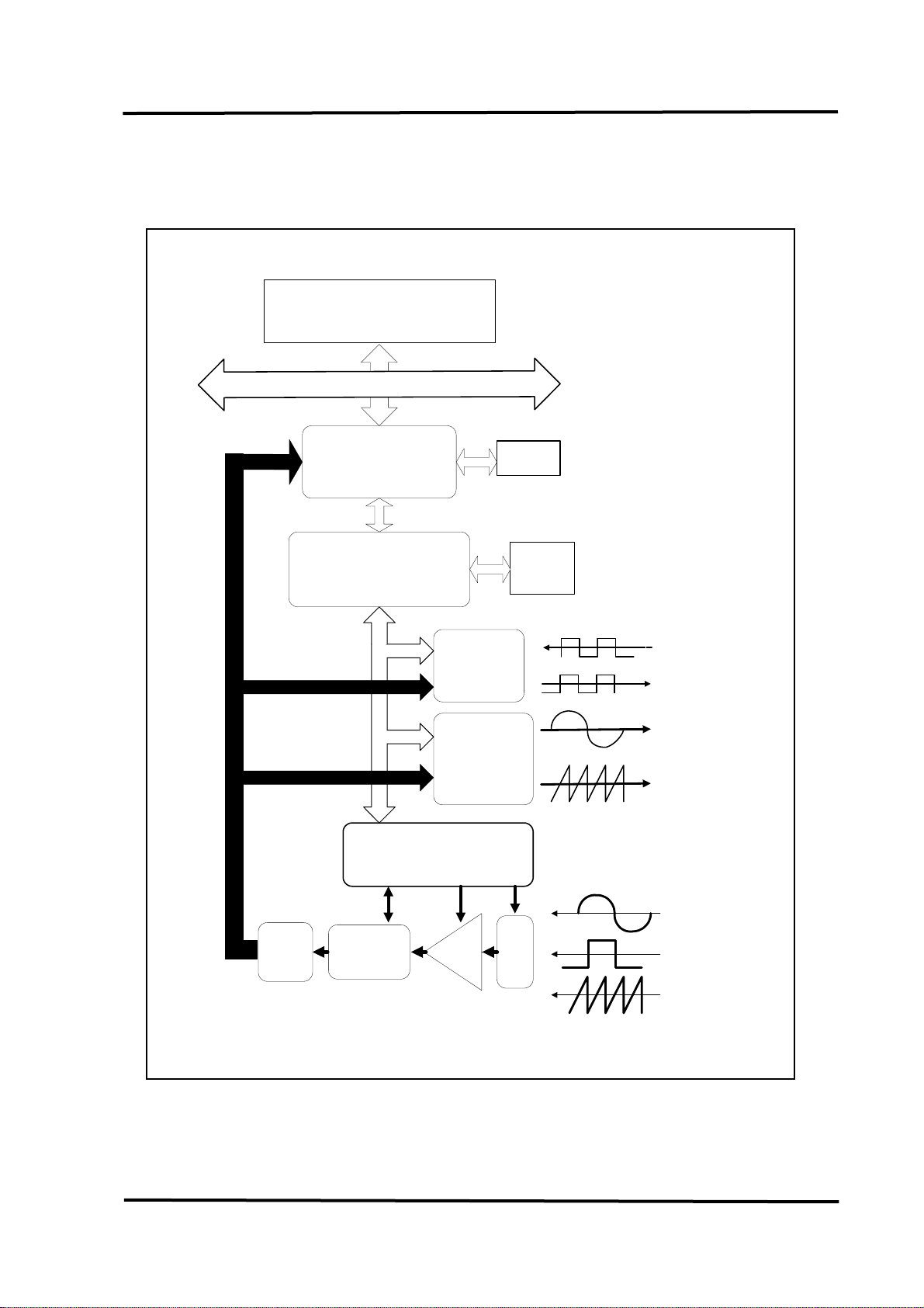
1.2 The Block Diagrams
The block diagram of OME-PCI-1202/1602/1800/1802 is given as follows:
X86 System
S
B
U
C
I
P
PCI Interface System
Local System Controller
16 bits DI
16 bits DO
2 channels
12 bit DA
Converter
Magic Scan Controller
EPROM
Status
Control
Digital Input
Digital Output
DAC OUT 0
DAC OUT 1
Analog Output
FIFO
1/2/4/8K
12/16bit A/D
Converter
MuxGain
Figure 1-1. The block diagram of OME-PCI-1202/1602/1800/1802.
6
Analog Input
Page 7

OME-PCI-1202/1602/1800/1802 Hardware User’s Manual
1.3 Features
The general features of OME-PCI-1202/1602/1800/1802 series are given as follows:
z Bus: 5V PCI (Peripherals Component Interconnect) bus.
z A/D:
1. OME-PCI-1800L/1802L: A/D converter = 330K samples/second
OME-PCI-1800H/1802H: A/D converter = 44K samples/second
OME-PCI-1602F: A/D converter = 200K samples/second
OME-PCI-1602: A/D converter = 100K samples/second
OME-PCI-1202L: A/D converter = 110K samples/second
OME-PCI-1202H: A/D converter = 44K samples/second
2. 32 single-ended / 16 differential analog inputs for OME-PCI-1202/1602/1802 H/L.
3. Three different A/D triggers: software, pacer and external trigger
. 4. Three different external triggers: pre-trigger, middle-trigger and post-trigger
5. Programmable input signal configuration.
6. “MagicScan” advanced scanning function
7. FIFO: 2K for OME-PCI-1202(H/L)/1800(H/L)
8K for OME-PCI-1602, OME-PCI-1602F and OME-PCI-1802(H/L)
z D/A:
1. Two channels independent 12 bits DACs.
2. Bipolar voltage output with +/-5V or +/- 10V jumper selectable.
3. High throughput: refer to chapter 10.
z DIO:
1. 16 channels TTL compatible DI and 16 channels TTL compatible DO .
2. High speed data transfer rate: refer to chapter 10.
z Timer:
1. Three 16-bits timer/counter (8254).
2. Timer 0 is used as the internal A/D pacer trigger timer.
3. Timer 1 is used as the external trigger timer.
4. Timer 2 is used as the machine independent timer for settling time delay.
7
Page 8

OME-PCI-1202/1602/1800/1802 Hardware User’s Manual
1.4 Specifications
1.4.1 Power Consumption:
z +5V @ 960mA maximum, OME-PCI-1202/1602/1800/1802.
z Operating temperature : 0°C to +70°C
1.4.2 Analog Inputs
z Channels: ( software programmable )
1. OME-PCI-1202/1602/1802: 32-single-ended/16-differential inputs, jumper select.
2. OME-PCI-1800: 16-single-ended/8-differential inputs, jumper select.
z Gain control: ( software programmable )
1. OME-PCI-1202/1800/1802 H: 0.5, 1, 5, 10, 50, 100, 500, 1000
2. OME-PCI-1202/1800/1802 L: 0.5, 1, 2, 4, 8
3. OME-PCI-1602/1602F: 1,2,4,8
z Bipolar input signal range :
1. OME-PCI-1202/1800/1802 L: ±10V,±5V, ±2.5V, ±1.25V, ±0.0625V
2. OME-PCI-1202/1800/1802 H: ±10V,±5V,±1V, ±0.5V, ±0.1V, ±0.05V, ±0.01V, ± 0.005V
3. OME-PCI-1602/1602F: ±10V,±5V,±2.5V,±1.25V
z Unipolar input signal range :
1. OME-PCI-1202/1800/1802 L: 0 to10V, 0 to5V, 0 to 2.5V, 0 to 1.25V
2. OME-PCI-1202/1800/1802 H: 0 to10V, 0 to1V, 0 to 0.1V, 0 to 0.01V
z Input current: 250 nA max (125 nA typical) at 25 °C.
z Over voltage : continuous single channel to 70Vp-p
z Input impedance :
OME-PCI-1202/1800/1802 H: 1010Ω // 6pF
OME-PCI-1202/1602/1800/1802 L: 1013Ω // 1pF
8
Page 9

OME-PCI-1202/1602/1800/1802 Hardware User’s Manual
1.4.3 A/D Converter
z Resolution: 12-bit for OME-PCI-1202/1800/1802 H/L
16-bit for OME-PCI-1602/1602F
z Conversion Cycle: 330K s/s for OME-PCI-1800L/1802L
44K s/s for OME-PCI-1800H/1802H
200K s/s for OME-PCI-1602F
100K s/s for OME-PCI-1602
110K s/s for OME-PCI-1202L
44K s/s for OME-PCI-1202H
z Internal sample and hold.
z 12-bit ADC Input Voltages and Output Codes for OME-PCI-1202/1800/1802 H/L
Analog Input Digital Output Binary Code Hex Code
+9.995V
0V
-4.88mv
-10V
MSB LSB
0111 1111 1111
0000 0000 0000
1111 1111 1111
1000 0000 0000
7FF
000
FFF
800
• 16-bit ADC Input Voltages and Output Codes for OME-PCI-1602/1602F
Analog Input Digital Output Binary Code Hex Code
+99.9V
+0V
-305µV
-10V
MSB LSB
0111 1111 1111 1111
0000 0000 0000 0000
1111 1111 1111 1111
1000 0000 0000 0000
7FFF
0000
FFFF
8000
9
Page 10
OME-PCI-1202/1602/1800/1802 Hardware User’s Manual
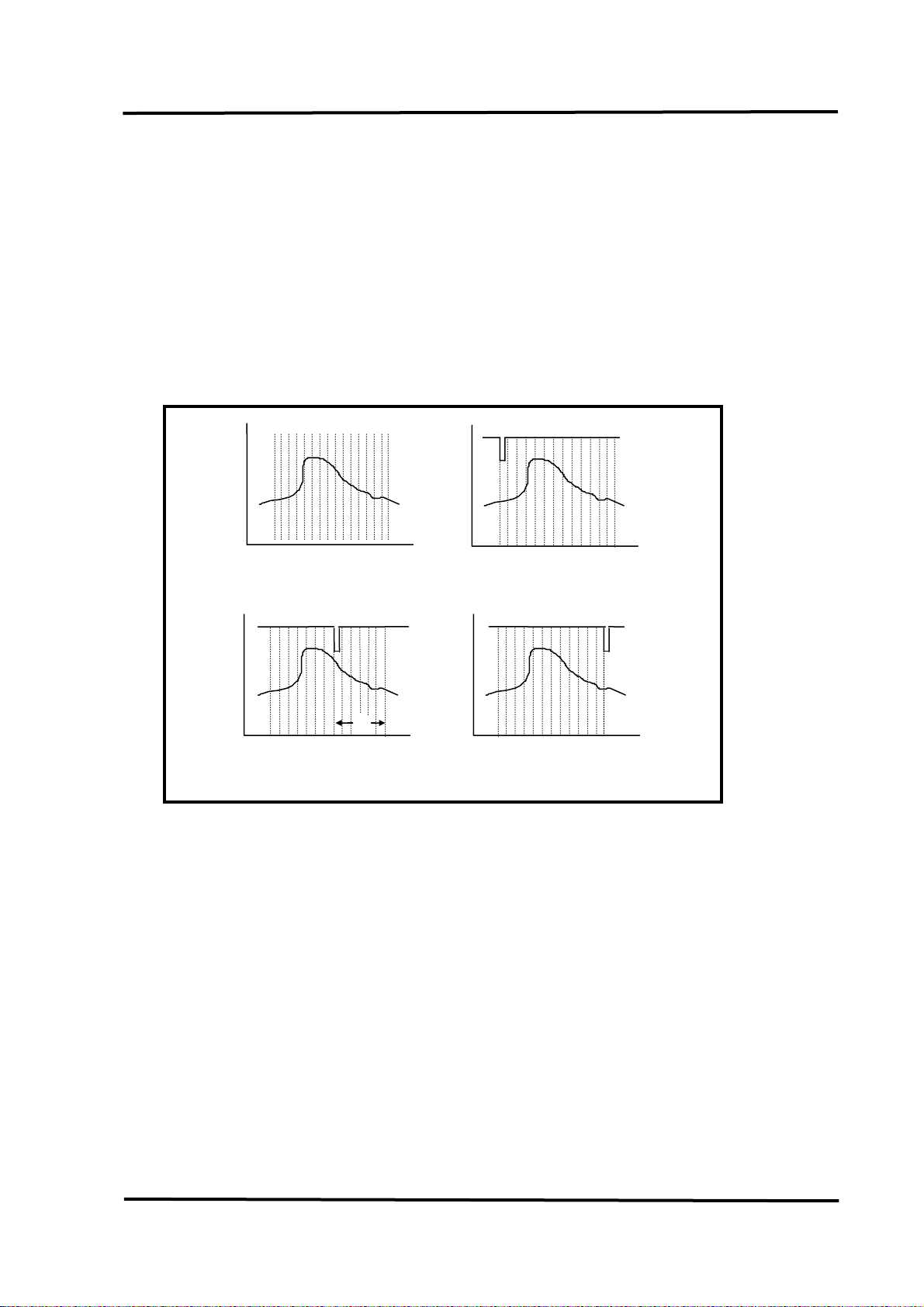
1.4.4 A/D Trigger Methods
z Trigger modes:
1. Internal software trigger
2. Internal pacer trigger
3. External trigger: pre-trigger, middle-trigger and post-trigger
CHn
CHn
External trigger
Start
Internal pacer trigger
t
Start
External post-trigger
External trigger
External trigger
CHn
CHn
External middle-trigger
N2
End
t
Start
External pre-trigger
Figure. 1-2. Trigger modes of OME-PCI-1202/1602/1800/1802.
t
t
10
Page 11

OME-PCI-1202/1602/1800/1802 Hardware User’s Manual
1.4.5 A/D Throughput
Throughput of OME-PCI-1800L/1802L
Gain Bipolar(V) Unipolar(V) Throughput
0.5 ±10V 0 to 10V 333 Ks/s
1 ±5V 0 to 10V 333 Ks/s
2 ±2.5V 0 to 5V 333 Ks/s
4 ±1.25V 0 to 2.5V 333 Ks/s
8 ±0.625V 0 to 1.25V 333 Ks/s
Throughput of OME-PCI-1602F/1602
Gain Bipolar(V) Throughput (1602F) Throughput (1602)
1 ±10V 200 Ks/s 100 Ks/s
2 ±5V 200 Ks/s 100 Ks/s
4 ±2.5V 200 Ks/s 100 Ks/s
8 ±1.25V 200 Ks/s 100 Ks/s
Throughput of OME-PCI-1202L
Gain Bipolar(V) Unipolar(V) Throughput
0.5 ±10V 0 to 10V 110 Ks/s
1 ±5V 0 to 10V 110 Ks/s
2 ±2.5V 0 to 5V 110 Ks/s
4 ±1.25V 0 to 2.5V 110 Ks/s
8 ±0.625V 0 to 1.25V 110 Ks/s
Throughput of OME-PCI-1202H/1800H/1802H
Gain Bipolar(V) Unipolar(V) Throughput
0.5/1 ±10/±5V 0 to 10V 40 Ks/s
5/10 ±1/±0.5V 0 to 1V 40 Ks/s
50/100 ±0.1/±0.05V 0 to 0.1V 10 Ks/s
500/1000 ±0.01/±0.005V 0 to 0.01V 1 Ks/s
11
Page 12

OME-PCI-1202/1602/1800/1802 Hardware User’s Manual
1.4.6 D/A Converter
z Channels: 2 independent.
z DAC Type: 12-bit multiplying DA converter.
z Accuracy: ±1 bit.
z Output type: 12-bit double buffered
z Output range: -5 to +5V or -10 to +10V jumper select.
z Output drive: ± 5mA
z Settling time: 0.4 µs (typical) to 0.01% for full scale step.
z Data transfer rate: 2.1 Mwords/second (non-burst mode).
12- bit DAC output code for OME-PCI-1202/1602/1800/1802 H/L
Data Input Analog Output
MSB LSB
1111 1111 1111
1000 0000 0001
1000 0000 0000
0111 1111 1111
0000 0000 0000
+Vref (2047/2048)
+Vref (1/2048)
0 Volts
-Vref (1/2048)
-Vref (2048/2048)
12
Page 13

OME-PCI-1202/1602/1800/1802 Hardware User’s Manual
1.4.7 Digital I/O
z Output port: 16-bit, TTL compatible
z Input port: 16-bit, TTL compatible
z Throughput: 2.1M word/sec (non-burst mode)
1.4.8 Interrupt Channel
z Interrupt: Automatically assigned by ROM BIOS.
z Enable/Disable: Via on-board control register.
1.4.9 Programmable Timer/Counter
z Type: 82C54 programmable timer/counter
z Timers: three 16-bit independent timer
1. Timer 0 is used as the internal A/D pacer trigger timer.
2. Timer 1 is used as the external trigger A/D pacer timer.
3. Timer 2 is used as the machine independent timer.
z Input clock: 8 MHz.
13
Page 14

OME-PCI-1202/1602/1800/1802 Hardware User’s Manual
1.5 Applications
z Signal analysis.
z FFT & frequency analysis.
z Transient analysis.
z Speech analysis.
z Temperature monitor.
z Production test.
z Process control.
z Vibration analysis.
z Energy management.
z Industrial and laboratory measurement and control.
1.6 Product Check List
In addition to this manual, the package includes the following items:
z OME-PCI-1202/1602/1800/1802 H/L multifunction card.
z NAPPCI/dos CD-ROM or diskette.
z Software User’s Manual on CD
Please read the release notes first, they contain the latest updates not found in this and the
other user manuals.
Note
If any of these items are missing or damaged, please contact OMEGA. It is
suggested that you save the shipping materials and carton in case you want to
ship or store the product in the future.
14
Page 15
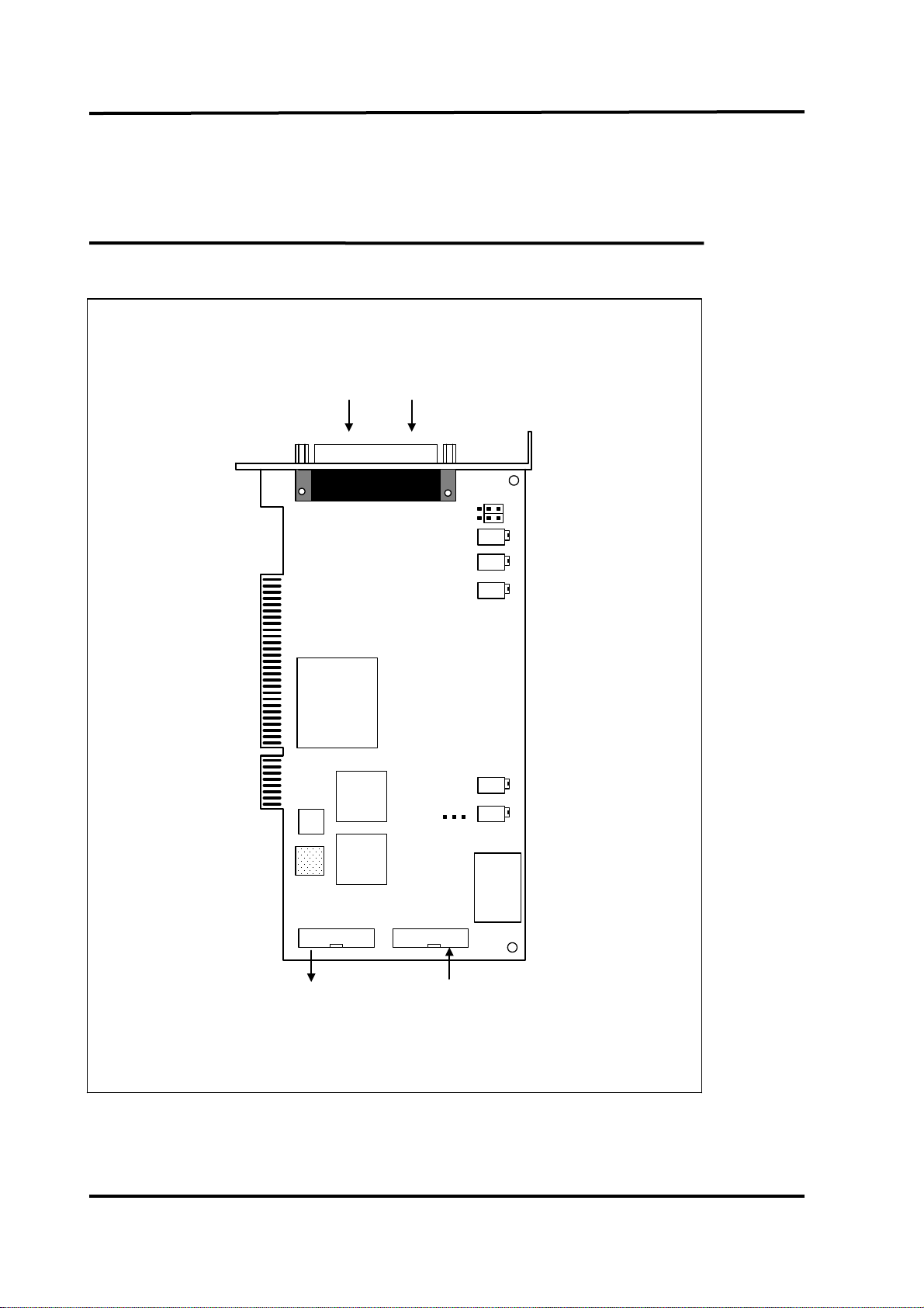
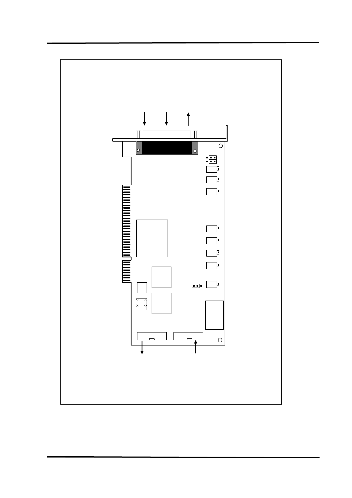
OME-PCI-1202/1602/1800/1802 Hardware User’s Manual
2. Hardware Configuration
2.1 Board Layout
ADC input
16 or 32
channels
External
Trigger Input
PCI-1800/1802L/NDA REV:C
CON3
JP1
1 2
5 6
VR1 VR101 VR2 VR3VR100
J1
10V
5V
CON1
16 channels
OUT
Digital Output
CON2
IN
Digital Input
16 channels
Figure 2-1. OME-PCI-180X(H/L) /NDA board layout.
15
Page 16
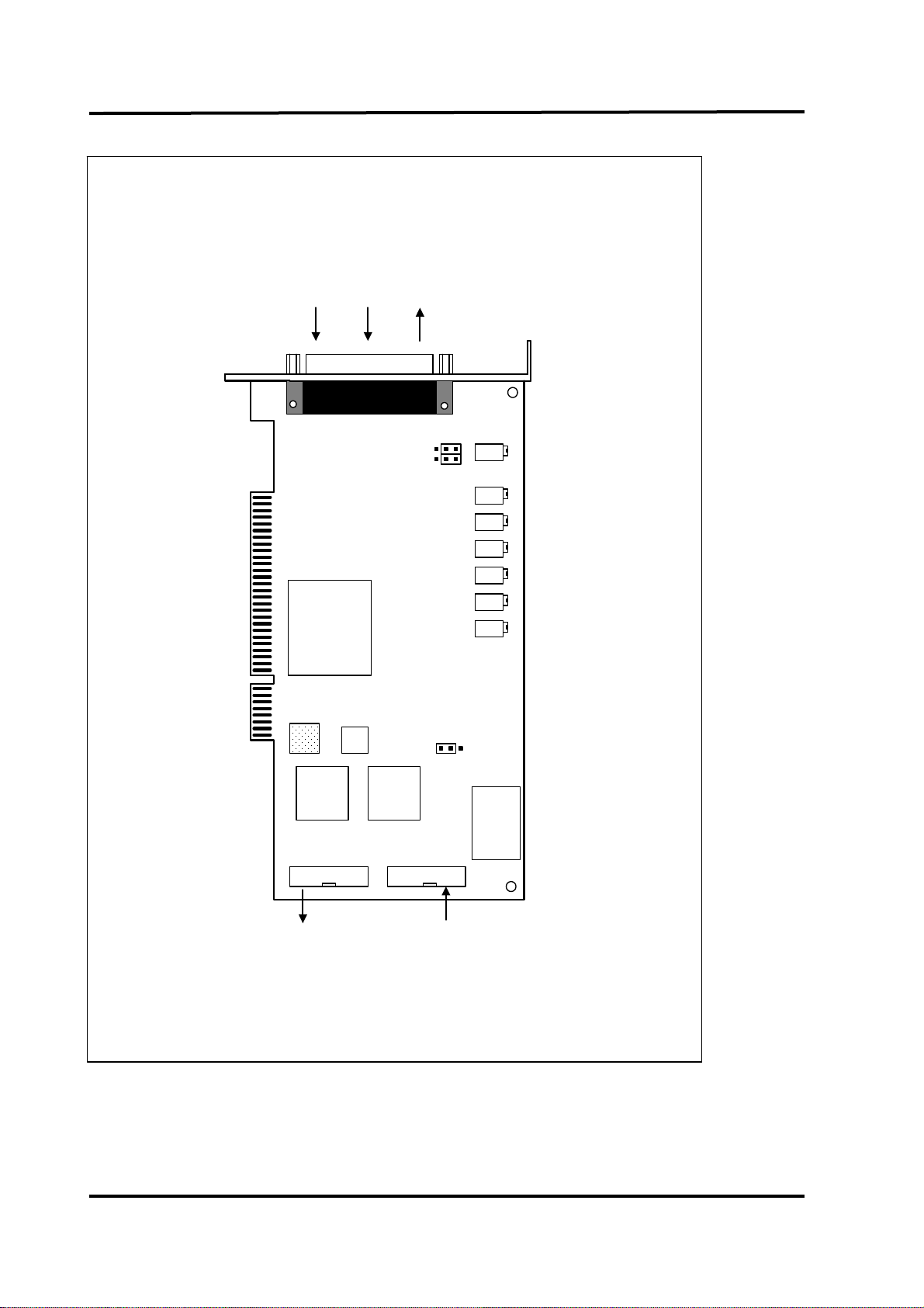
OME-PCI-1202/1602/1800/1802 Hardware User’s Manual
External
Trigger Input
16 or 32
channels
ADC input
DAC output
2 channels
PCI-1800/1802L REV:F
CON3
5 6
1 2
JP1
VR1 VR101
CON1
Digital Output
16 channels
OUT
CON2
J1
IN
5V
16 channels
VR201 VR202
VR200VR100
VR203
VR2
10V
Digital Input
Figure 2-2. OME-PCI-1202(H/L)/1800(H/L)/1802(H/L) board layout.
16
Page 17
OME-PCI-1202/1602/1800/1802 Hardware User’s Manual
DAC output
2 channels
ADC input
32 channels
External
Trigger Input
PCI-1602/1602F REV:1.0
CON3
1
5
JP1
2
6
10V
5V
VR1 VR3
VR2 VR4
VR5 VR6
VR7
J1
CON1
OUT
Digital Output
16 channels
IN
16 channels
Figure 2-3. OME-PCI-1602/1602F board layout.
17
CON2
Digital Input
Page 18
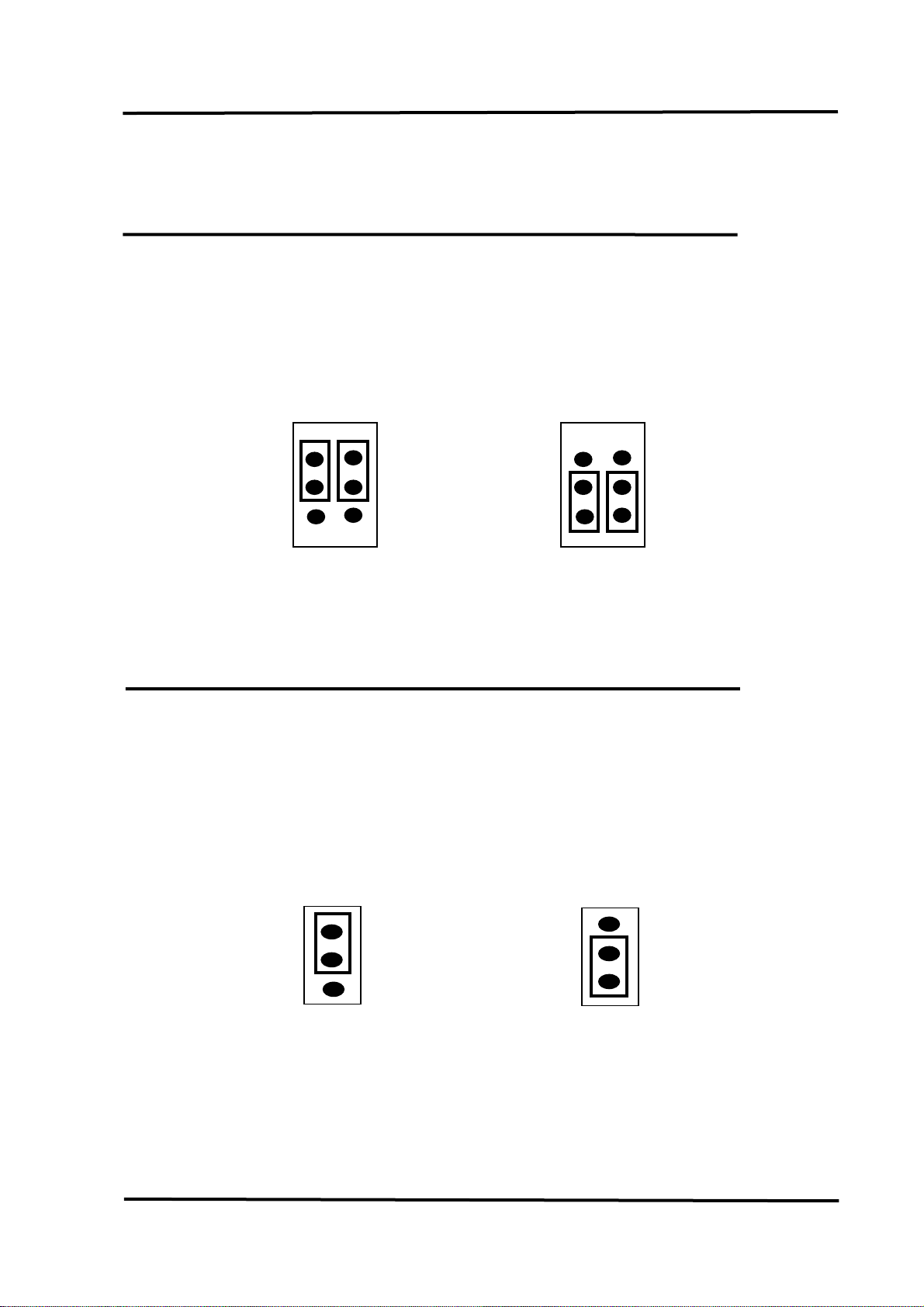
OME-PCI-1202/1602/1800/1802 Hardware User’s Manual
)
2.2 Jumper Setting
2.2.1 JP1: A/D Input Type Selection
This jumper is used to select the analog input type. For single-ended inputs, connect
pin 1,3 and pin 2,4. For differential inputs, pin 3,5 and pin 4,6 should be connected.
JP1 JP1
1
5 6
Single-Ended
Inputs (default
2
1
5
Differential
Inputs
2
6
2.2.2 J1: D/A Reference Voltage Selection
J1 is used to select the internal D/A output reference voltage. To select the ±10V
output, pin 1&2 should be connected. To select the ±5V output, pin 2&3 should be
connected.
J1 J1
1
± 10 Voltage
output (default)
18
1
± 5 Voltage
output
Page 19
OME-PCI-1202/1602/1800/1802 Hardware User’s Manual
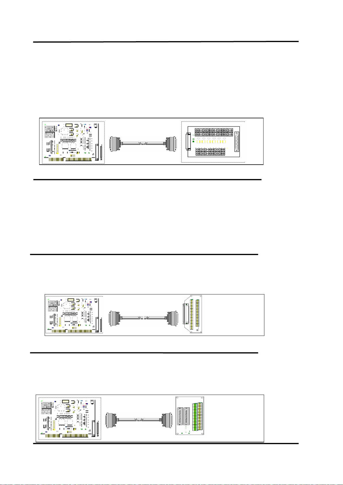
2.3 Daughter Boards
2.3.1 OME-DB-1825
The OME-DB-1825 is a daughter board designed for 32-channel AD cards such as the
OME-PCI-1202/1602/1802. Refer to Appendix A for details on the OME-DB-1825.
37pin cable
2.3.2 OME-DB-8225
The OME-DB-8225 provides a on-board CJC (Cold Junction Compensation) circuit for
thermocouple measurement and a terminal block for easy signal connection. The CJC is
connected to A/D channel_0. The OME-PCI-1800 can connect CON3 direct to an OME-DB-
8225 through a 37-pin D-sub connector. Refer to the OME-DB-8225 User Manual for details.
2.3.3 OME-DB-37
The OME-DB-37 is a general purpose daughter board for D-sub 37 pins. It is designed
for easy wire connection.
2.3.4 OME-DN-37
The OME-DN-37 is a general purpose daughter board for DIN Rail Mounting. It is
designed for easy wire connection and DIN-Rail mounting.
37pin cable
19
Page 20
OME-PCI-1202/1602/1800/1802 Hardware User’s Manual
2.3.5 OME-DB-16P Isolated Input Board
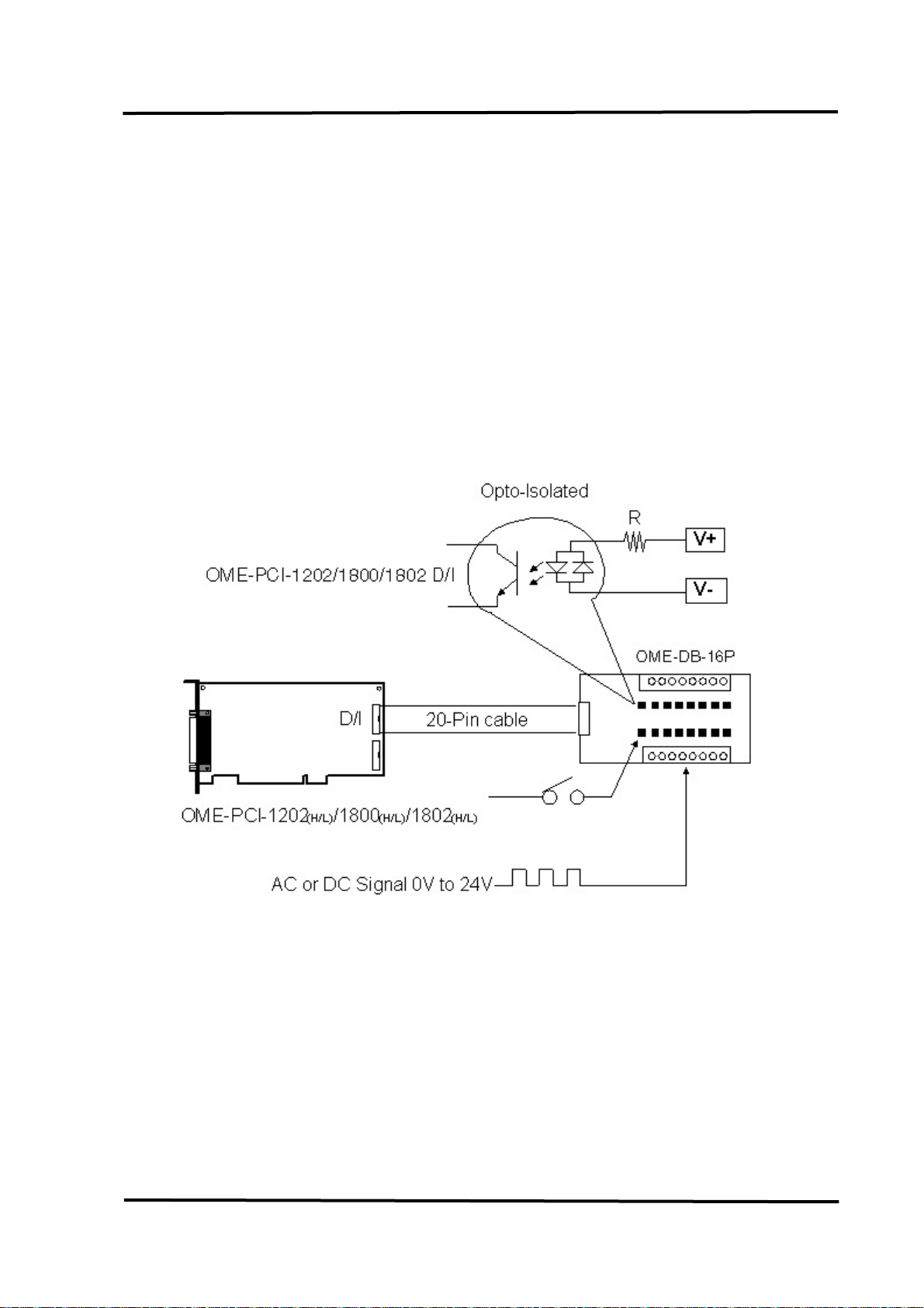
The OME-DB-16P is a 16-channel isolated digital input daughter board. The optically
isolated inputs of the OME-DB-16P consist of a bi-directional optocoupler with a resistor for
current sensing. You can use the OME-DB-16P to sense DC signals from TTL levels up to 24V
or use the OME-DB-16P to sense a wide range of AC signals. You can use this board to isolate
the computer from large common-mode voltages, ground loops and transient voltage spikes
that often occur in industrial environments.
20
Page 21
OME-PCI-1202/1602/1800/1802 Hardware User’s Manual
2.3.6 OME-DB-16R Relay Board
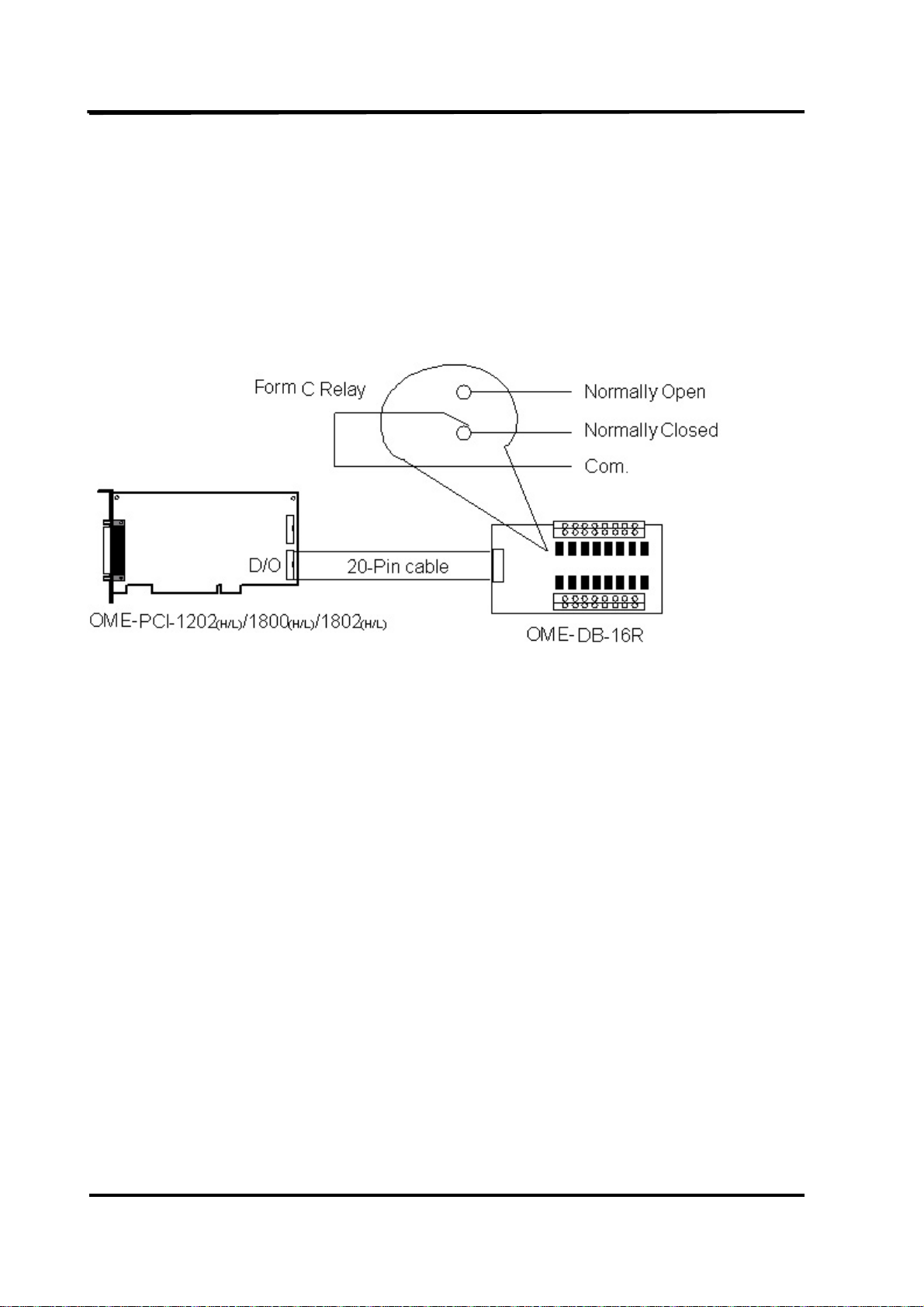
The OME-DB-16R, 16-channel relay output board consists of 16 from C relays used for
switching loads under program control. Applying 5 volts to the appropriated relay channel on
the 20-pin flat connector energizes the relays. There is 16 status LEDs for each relay, which
light when their associated relay is activated. To avoid overloading your PC’s power supply,
this board provides a screw terminal connection an for external power supply.
Note: Channel: 16 Form C Relay
Relay: Switching up to 0.5A at 110ACV or 1A at 24 DCV
21
Page 22
OME-PCI-1202/1602/1800/1802 Hardware User’s Manual
2.3.7 OME-DB-24PR Power Relay Board
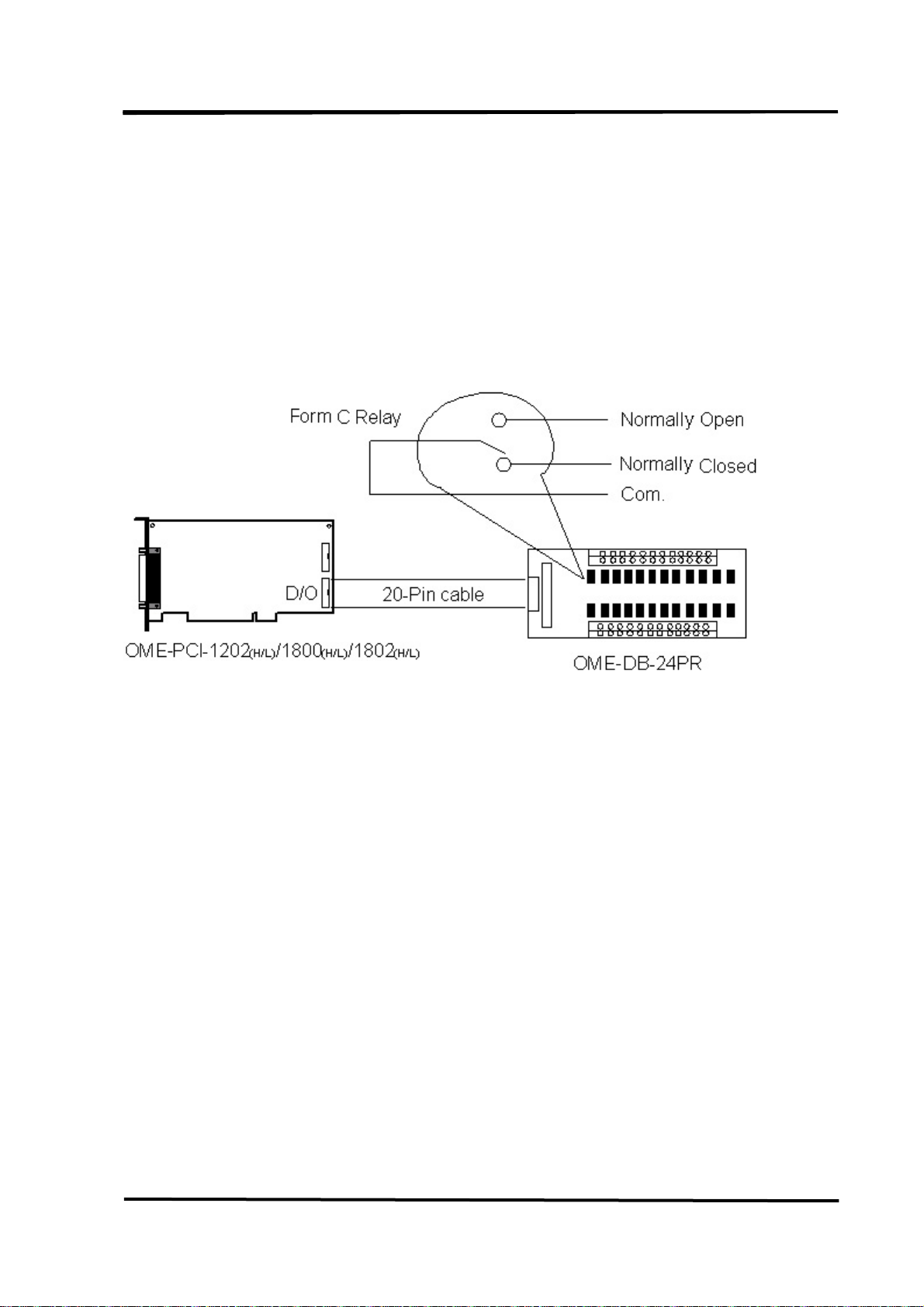
The OME-DB-24PR, 24-channel power relay output board consists of 8 form C and 16
form A electromechanical relays for switching a load under program control. Each relay
contact is rated to 5A at 250ACV/30VDCV. The relay is energized by applying a 5 volt signal
to the appropriate relay channel on the 20-pin flat cable connector or 50-pin flat cable
connector. Each channel has an LED which will light when the associated relay is activated.
To avoid overloading your PC’s power supply, the board requires a +12VDC or +24VDC
external power supply.
Channel: 16 Form A Relays, 8 Form C Relays
Relay: Switching up to 5A at 110ACV / 5A at 30DCV
22
Page 23

OME-PCI-1202/1602/1800/1802 Hardware User’s Manual
2.4 Analog Input Signal Connection
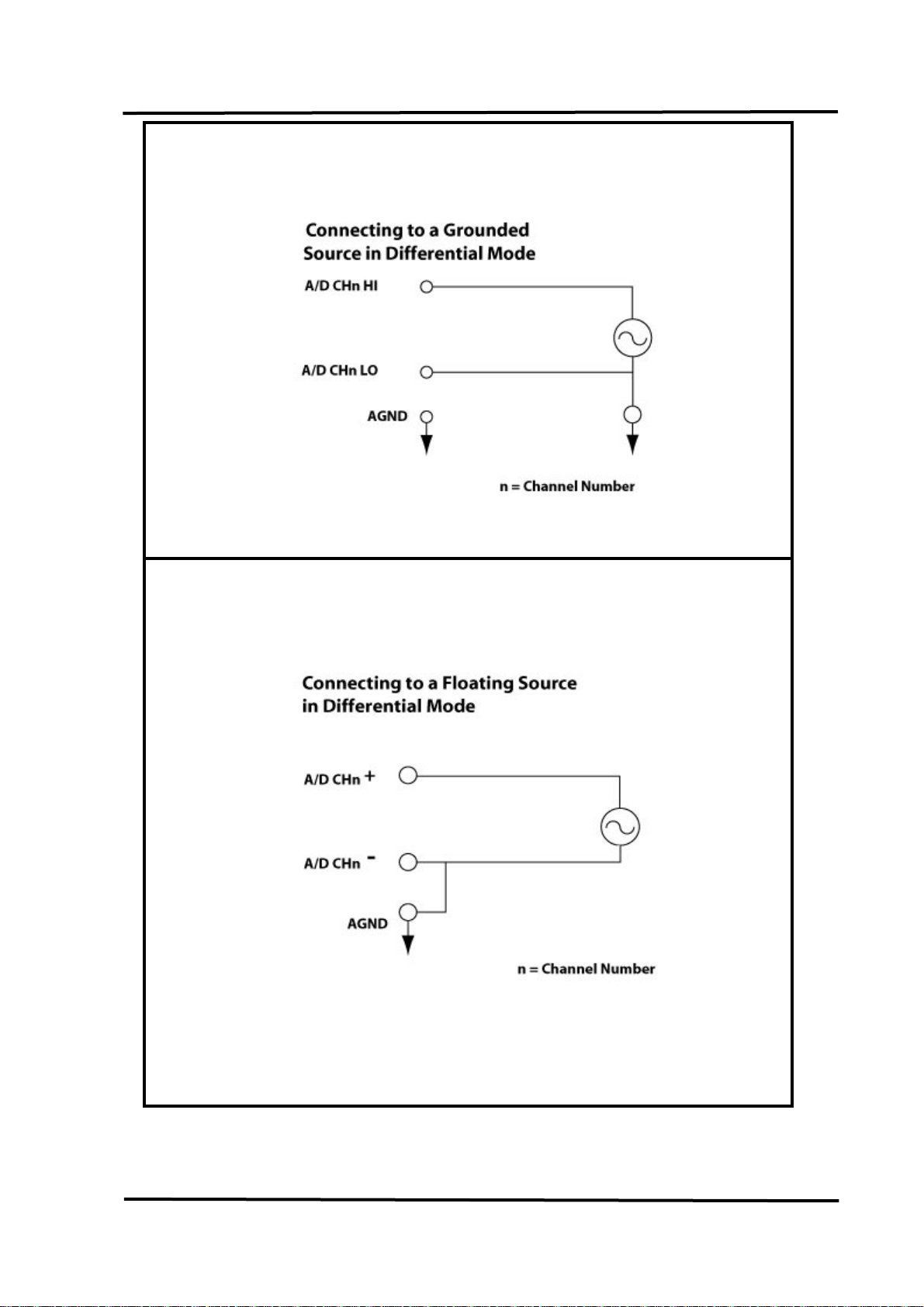
The OME-PCI-1202/1602/1800/1802 can measure signals in the single-ended or
differential mode. In the differential mode each channel has a unique signal HIGH and signal
LOW connection. In the single-ended mode all channels have a unique signal HIGH
connection but share a common LOW or ground connection. Differential connections are very
useful for low level signals (millivolt), since they better reject electrical noise that can affect
the quality of the measurement. A differential connection is also necessary when a common
ground is unacceptable. The benefit of using a single-ended connection is that twice the
number of channels is available. In general, a single-ended connection is often a good choice
when working with higher level signals (5V or 10V for example), especially if the signal is
coming from an isolated device such as a signal conditioner. Several different types of wiring
diagrams are discussed below.
Figure 2-4A shows a differential connection to a grounded source. If the source is
grounded, making a second connection to the card’s ground could cause a ground loop
resulting in erroneous data. It is important to note that the maximum common mode
voltage between the input source and AGND is 70Vp-p. If the card is connected to a
source with a common mode voltage greater than 70Vp-p, the input multiplexer will be
permanently damaged! When measuring common mode voltage, it is best to use an
oscilloscope rather than a multi-meter.
Figure 2-4B shows a differential connection to a floating source. In such cases a
connection should be made between the low channel input and analog ground.
Figure 2-5 shows connection of multiple sources in single-ended mode. This connection
assumes creating one common ground will not cause a problem. This is normally the case
when connecting to devices that are isolated or floating.
Figure 2-6 demonstrates how to connect bridge transducers. Bridge transducers include
strain gauges, load cells and certain type of pressure transducers. The diagram assumes that
there is a single external power supply providing power to the bridge. Each bridge is
connected to a differential channel. No connection is made between channel low and analog
ground. A connection should be made between analog ground and the negative of the power
supply. An isolated power supply is strongly suggested.
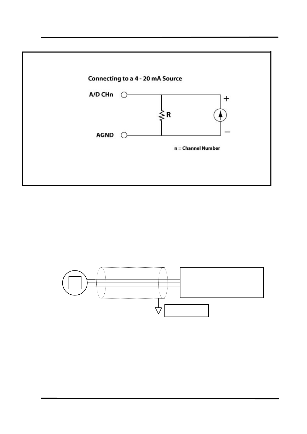
Figure 2-7 demonstrates how to connect a 4-20mA current loop. Since the card reads
voltages, the current is converted to voltage by passing it through a shunt resistor. By Ohms
law (V=IR), when using a 250Ω resistor, 4 mA will be converted to 1 volt and 20mA to 5V. If
the source is linear, the output voltage range will also be linear.
23
Page 24
OME-PCI-1202/1602/1800/1802 Hardware User’s Manual
Figure 2-4A
If the source is grounded, a second ground connection
on the card could result in a ground loop.
Figure 2-4B
24
Page 25
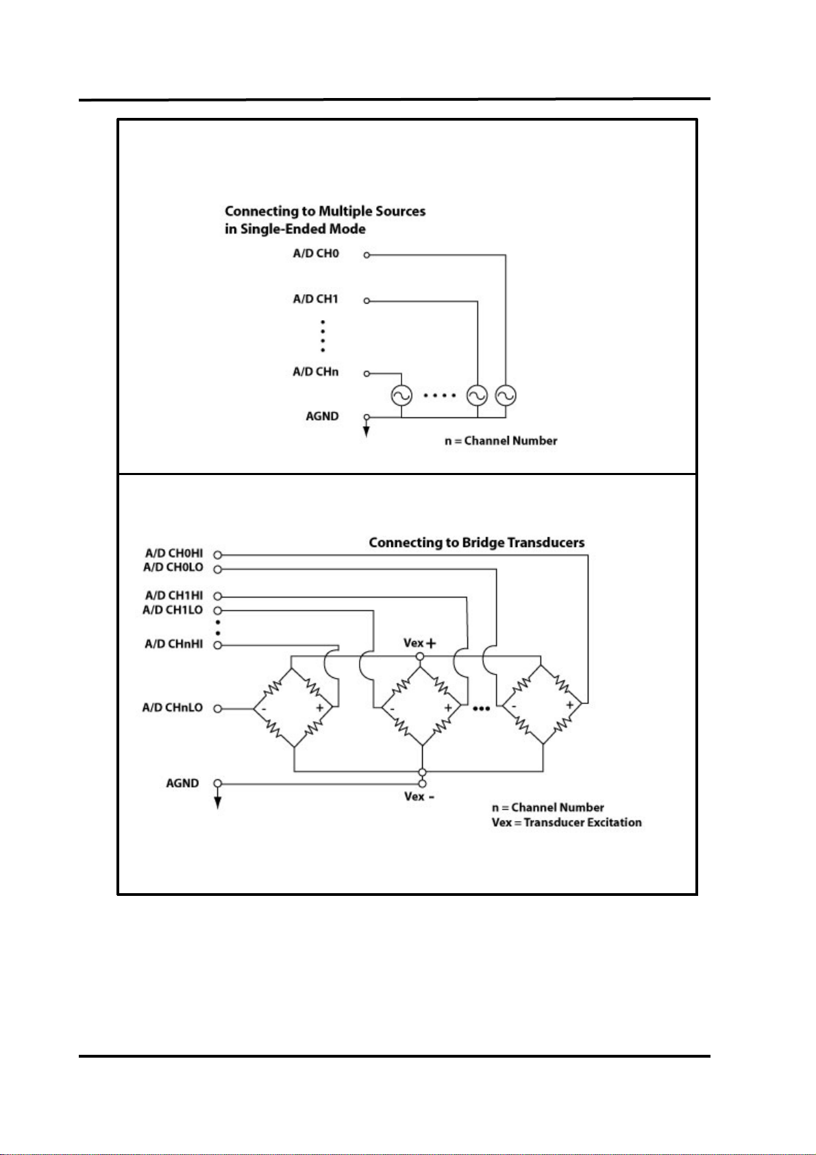
Figure 2-5
OME-PCI-1202/1602/1800/1802 Hardware User’s Manual
Figure 2-6
25
Page 26
OME-PCI-1202/1602/1800/1802 Hardware User’s Manual
Figure 2-7
R is a shunt resistor. A 250Ω shunt resistor converts 4-20mA to 1-5Vdc.
Signal Shielding
z The signal shielding connections in Figure 2-4 to Figure 2-7 are all the same
z Use a single connection to frame ground (not A.GND or D.GND)
Vin
OME-PCI-1202/1602/1800/1802
A.GND
D.GND
Frame Ground
26
Page 27

OME-PCI-1202/1602/1800/1802 Hardware User’s Manual
2.5 The Connectors
CON1: Pin assignment of the digital output connector
Pin Name Pin Name
1 Digital output 0 2 Digital output 1
3 Digital output 2 4 Digital output 3
5 Digital output 4 6 Digital output 5
17 Digital output 6 8 Digital output 7
9 Digital output 8 10 Digital output 9
11 Digital output 10 12 Digital output 11
13 Digital output 12 14 Digital output 13
15 Digital output 14 16 Digital output 15
17 PCB ground 18 PCB ground
19 PCB +5V 20 PCB +12V
CON2: Pin assignment of digital input connector
Pin Name Pin Name
1 Digital input 0 2 Digital input 1
3 Digital input 2 4 Digital input 3
5 Digital input 4 6 Digital input 5
7 Digital input 6 8 Digital input 7
9 Digital input 8 10 Digital input 9
11 Digital input 10 12 Digital input 11
13 Digital input 12 14 Digital input 13
15 Digital input 14 16 Digital input 15
17 PCB ground 18 PCB ground
19 PCB +5V 20 PCB +12V
27
Page 28

OME-PCI-1202/1602/1800/1802 Hardware User’s Manual
C0N3: pin assignment of single-ended/differential inputs (for OME-PCI-
1202/1602/1802H/L)
Pin Name Pin Name
1 Analog input 0/0+ 20 Analog input 16/0-
2 Analog input 1/1+ 21 Analog input 17/1-
3 Analog input 2/2+ 22 Analog input 18/2-
4 Analog input 3/3+ 23 Analog input 19/3-
5 Analog input 4/4+ 24 Analog input 20/4-
6 Analog input 5/5+ 25 Analog input 21/5-
7 Analog input 6/6+ 26 Analog input 22/6-
8 Analog input 7/7+ 27 Analog input 23/7-
9 Analog input 8/8+ 28 Analog input 24/8-
10 Analog input 9/9+ 29 Analog input 25/9-
11 Analog input 10/10+ 30 Analog input 26/10-
12 Analog input 11/11+ 31 Analog input 27/11-
13 Analog input 12/12+ 32 Analog input 28/12-
14 Analog input 13/13+ 33 Analog input 29/13-
15 Analog input 14/14+ 34 Analog input 30/14-
16 Analog input 15/15+ 35 Analog input 31/15-
17 Analog ground 36 Analog output 1
18 Analog output 0 37 Digital ground
19 External trigger
28
Page 29

OME-PCI-1202/1602/1800/1802 Hardware User’s Manual
CON3: pin assignment of single-ended/differential input.(for OME-PCI-1800H/L)
Pin Name Pin Name
1 Analog input 0/0+ 20 Analog input 8/0-
2 Analog input 1/1+ 21 Analog input 9/1-
3 Analog input 2/2+ 22 Analog input 10/2-
4 Analog input 3/3+ 23 Analog input 11/3-
5 Analog input 4/4+ 24 Analog input 12/4-
6 Analog input 5/5+ 25 Analog input 13/5-
7 Analog input 6/6+ 26 Analog input 14/6-
8 Analog input 7/7+ 27 Analog input 15/7-
9 Analog Ground 28 Analog Ground
10 Analog Ground 29 Analog Ground
11 N.C. 30 Analog output 0
12 N.C. 31 N.C.
13 PCB +12V 32 Analog output 1
14 Analog Ground 33 N.C.
15 Digital Ground 34 N.C.
16 N.C. 35 N.C.
17 External Trigger 36 N.C.
18 N.C. 37 N.C.
19 PCB +5V
N. C.: Abbreviation of “Not Connected “.
29
Page 30

OME-PCI-1202/1602/1800/1802 Hardware User’s Manual
3. I/O Control Register
3.1 How to Find the I/O Address
During the computer’s power-on stage the plug&play BIOS will assign a valid I/O address
to each OME-PCI-1800/1802 card. The P180X_DriverInit(..) can detect how many OME-
PCI-1800/1802 cards are in the system and the I/O addresses of these cards. The
P180X_DriverInit(..) is supported in both DOS and Windows driver versions. The
P180X_DriverInit(..) must be called before any other driver function. The
P180X_DriverInit(..) will:
1. Detect how many OME-PCI-1800/1802 cards in the system?
2. Detect and save the I/O control address of every OME-PCI-1800/1802 card
Sample program code is shown below:
wRetVal=P180X_DriverInit(&wBoards); /* call P180X_DriverInit(..) first */
printf("Threre are %d P180X Cards in this PC\n",wBoards);
/* dump every P180X card's configuration address space */
printf("The Configuration Space -> Timer Control DIO AD/DA \n");
for (i=0; i<wBoards; i++)
{
printf("Card %02d: %04xH %04xH %04xH %04xH\n", i,wConfigSpace[i][0],
wConfigSpace[i][1], wConfigSpace[i][2],wConfigSpace[i][3]);
}
/* The P180X_ActiveBoard() function must be used to activate a board, */
/* then all operations will apply to the active board. */
printf("Now Active First P180X Card...\n");
P180X_ActiveBoard( 0 );
z P1202_DriverInit(…) is designed for OME-PCI-1202H/L
z P1602_DriverInit(…) is designed for OME-PCI-1602 andOME-PCI-1602F
30
Page 31

OME-PCI-1202/1602/1800/1802 Hardware User’s Manual
3.2 The Assignment of I/O Address
The plug & play BIOS will assign a valid I/O address to OME-PCI-
1202/1602/1800/1802. If there is only one OME-PCI-1202/1602/1800/1802, the user can
easily identify board_1. If there are two OME-PCI-1202/1602/1800/1802 cards in the system,
identifying each board is a little more complicated. The software driver can support up to 16
boards. Therefore the user can install 16 boards in one PC system.
The simplest way to find the board number is to use the DEMO15.EXE program.
This demo program will send a value the digital output and read back from digital input. If
the user installs a 20-pin flat cable between CON1 & CON2, the value read from digital input
will be the same as digital output. The steps are given as follows:
1. If present, remove the 20-pin flat cable between CON1 and CON2
2. Install the OME-PCI-1202/1602/1800/1802 cards into the PC
3. Power-on and run DEMO15.EXE
4. At this time, all D/I values will be different from the D/O values
5. Install on any OME-PCI-1202/1602/1800/1802 card, a 20-pin flat cable between
CON1 & CON2
6. In the software one of the cards will have the same D/I value and D/O value. That is
the card with the cable.
7. Repeat the process to identify the remaining cards
3.3 The I/O Address Map
The I/O address of OME-PCI-1202/1602/1800/1802 is automatically assigned by
the computer’s ROM BIOS. The I/O address can also be reassigned by the user. It is
strongly recommended that the user not change the I/O address assigned by the
BIOS. There are five sections of I/O addresses used by this card and each section can
be assigned to an unused I/O space. The hardware I/O ports are described below:
31
Page 32

OME-PCI-1202/1602/1800/1802 Hardware User’s Manual
Section Address Name Operation Access
1
2
3
4
Section1 + 0h PCI controller add-on
W 32-bits
mail box
Section1 + 38h PCI interrupt control
R/W 32bits
register
Section1 + 3Ch
(or 3Eh, 3Fh)
On board NV-RAM
access control register
R/W 32 bits
(8 bits)
Section2 + 00h 8254 timer1 R/W 8/16/32 bits
Section2 + 04h 8254 timer2 R/W 8/16/32 bits
Section2 + 08h 8254 timer3 R/W 8/16/32 bits
Section2 + 0Ch 8254 control W 8/16/32 bits
Section3 +00h Control register W 16/32 bits
Section3 + 00h Status register R 8/16/32 bits
Section3 + 04h A/D sofware trigger W 8/16/32 bits
Section4 + 00h DI port R 16 bits
Section4 + 00h DO port W 16 bits
Section5 + 00h A/D data port R 16 bits
5
Section5 + 00h D/A channel 1. W 16 bits
Section5 + 04h D/A channel 2. W 16 bits
The driver name of these address are given as follows:
section_2 : wAddrTimer Æ save in wConfigSpace[Board][0]
section_3 : wAddrCtrl Æ save in wConfigSpace[Board][1]
section_4 : wAddrDio Æ save in wConfigSpace[Board][2]
section_5 : wAddrAdda Æ save in wConfigSpace[Board][3]
32
Page 33

OME-PCI-1202/1602/1800/1802 Hardware User’s Manual
3.4 Section 1: PCI Controller
Although 64 I/O ports are used by the on-board OME-PCI-controller, only 3 registers
can be directly accessed by the user.
Address Access Functions Operation
+3C
+ 0
+38
+3F
(8bits)
Write only
(32 bit)
Write
(32bit)
Read (32bit)
Write
(8bit)
Read
Out-going mail-box Write a 0 to wait for add-on interrupt.
Enable/Re-enable/
Disable target interrupt
Read interrupt status.
Write command to
nvRAM control register
Read status from
1. Enable : Write 00010010h to this
port.
2. Re-enable: Write 00010010h to
this port.
3. Disable : Write 0 to this port.
Bit 16 : 1 Æ interrupt generated.
0 Æ no interrupt.
0x80 : load low address
0xA0: load high address
0xC0: begin write.
0xE0: begin read.
Bit 7 : 1 Æ busy
(32bit)
+3E
(8bits)
The user does not normally need to access this register. Refer to “AMCC S5933 PCI
Controllers User Manual” for all registers details.
(8bit)
Write
(8bit)
Read
(8bit)
nvRAM control register
Write nvRAM address or
nvRAM data to register. After finish writing to nvRAM control
Read nvRAM data from
this register.
33
0 Æ ready
register, write data to this port.
After finish writing to nvRAM control
register, read data from this port..
Page 34

OME-PCI-1202/1602/1800/1802 Hardware User’s Manual
3.5 Section 2: Timer Control
The timer-0 is used as the internal trigger A/D pacer timer. The timer-1 is used for the
external trigger pacer timer. The timer-2 is used as the machine independent timer. Timer-2 is
used for settling time delay, a critical function. Refer to Intel’s “Microsystem Components
Handbook” for 8254 programming. The block diagram of the 8254 timer is show below:
8Mhz
CLK
Timer 0
OUT0
Internal Pacer timer
Local Data Bus
D0,D1 ... D7
CLK
Timer 1
OUT1
CLK
Timer 2
OUT2
ADC
External Pacer timer
Machine indenpedent Timer
Figure 3-1: The block diagram of OME-PCI-1202/1602/1800/1802 8254 timer.
The I/O address of 8254 timer is given as follows:
z I/O address of timer/counter_0 = wAddrTimer+0*4
z I/O address of timer/counter_1 = wAddrTimer+1*4
z I/O address of timer/counter_2 = wAddrTimer+2*4
z I/O address of control register = wAddrTimer+3*4
34
Page 35

OME-PCI-1202/1602/1800/1802 Hardware User’s Manual
// timer0 Æ for pacer trigger
void enable_timer0(WORD divv) // for internal pacer trigger
{
outport((WORD)(wAddrTimer+3*4), 0x34); /* enable pacer timer_0 */
outport((WORD)(wAddrTimer+0*4), (WORD)(divv & 0xff));
outport((WORD)(wAddrTimer+0*4), (WORD)((divv>>8) & 0xff));
}
void disable_timer0(void)
{
outport((WORD)(wAddrTimer+3*4), 0x34); /* disable pacer timer_0 */
outport((WORD)(wAddrTimer+0*4), 0x01);
outport((WORD)(wAddrTimer+0*4), 0x00);
}
// timer1 Æ for external trigger
void enable_timer1(WORD divv) /* for external trigger pacer timer */
{
outport((WORD)(wAddrTimer+3*4), 0x74); /* enable pacer timer_1 */
outport((WORD)(wAddrTimer+1*4), (WORD)(divv & 0xff));
outport((WORD)(wAddrTimer+1*4), (WORD)((divv>>8) & 0xff));
}
void disable_timer1(void)
{
outport((WORD)(wAddrTimer+3*4), 0x74); /* disable timer_1 */
outport((WORD)(wAddrTimer+1*4), 0x01);
outport((WORD)(wAddrTimer+1*4), 0x00);
}
35
Page 36

OME-PCI-1202/1602/1800/1802 Hardware User’s Manual
// timer2 Æ for Machine Independent Timer
/* address of timer 2 = wAddrTimer+2*4
address of ctrl = wAddrTimer+3*4
input clock = 8M
down count 8 time = 1 us
down count 65536/8 = 8192 uS --> max 8191 uS
*/
WORD P180X_DelayUs(WORD wDelayUs)
{
WORD wDownCount,wLow,wHigh,wVal;
double fTimeOut;
if (wDelayUs>=8191) return(InvalidateDelay);
wDownCount=wDelayUs*8;
wLow=wDownCount&0xff;
wHigh=(wDownCount>>8)&0xff;
outport((wAddrTimer+3*4), 0xb0); /* timer_2 mode_0 0xb0 */
outport((wAddrTimer+2*4), wLow);
outport((wAddrTimer+2*4), wHigh);
fTimeOut=1.0; // wait 1 to stop
for (;;)
{
wVal=inport(wAddrCtrl)&0x01;
if (wVal!=0) return(NoError); /* if the timer is up, this bit will be 1 */
fTimeOut+=1.0;
if (fTimeOut>6553500.0)
return(DelayTimeOut);
}
}
z P1202_DelayUs(…) is designed forOME-PCI-1202H/L
z P1602_DelayUs(…) is designed forOME-PCI-1602 andOME-PCI-1602F
36
Page 37

OME-PCI-1202/1602/1800/1802 Hardware User’s Manual
3.6 Section 3: Control Register
z I/O address of control register = wAddrCtrl + 0
z I/O address of status register = wAddrCtrl + 0
z I/O address of trigger register = wAddrCtrl + 1 *4
The flow path of analog input signal is given as follows:
Signals
Max=+/-10V Max=+/-5V
Single-ended
Differential
MUX
4,3,2,1,0 7,6
AMP1
Gain Rang
Figure 3-2: The flow diagram of an analog input signal.
3.6.1 The Control Register
The format of the control register is given as follows:
AMP1
9,8
ADC
0
1
0
:
:
:
:
.
1
B15 B14 B13 B12 toB10 B9, B8 B7, B6 B5 B4 to B0
z B4 - B0: A/D channel select
z B7, B6: A/D gain control.
z B9, B8: A/D input range control.
z B12 -B10: external trigger control.
z B13: handshake control to MagicScan controller.
z B15: clear FIFO.
z B5, B14: reserved
37
Page 38

OME-PCI-1202/1602/1800/1802 Hardware User’s Manual
3.6.1.1 Bit4 - Bit0: A/D channel select
A/D channel B4 B3 B2 B1 B0
0 0 0 0 0 0 1800/1202/1602/1802
15 0 1 1 1 1 1800/1202/1602/1802
16 1 0 0 0 0 1202/1602/1802
31 1 1 1 1 1 1202/1602/1802
3.6.1.2 Gain control
[B7, B6] PCI-1XXXL PCI-1XXXH
[0, 0] PGA=1 PGA=1
[0, 1] PGA=2 PGA=10
[1, 0] PGA=4 PGA=100
[1, 1] PGA=8 PGA=1000
3.6.1.3 Input Range Control
[B9, B8] Output
[0, 0] PGA
[1, 0] PGA-5
[0, 1] PGA/2
[1, 1] PGA/2 - 5
38
Page 39

OME-PCI-1202/1602/1800/1802 Hardware User’s Manual
3.6.1.4 Configuration Table
Configuration table for OME-PCI-1202L/1800L/1802L
Bipolar/Unipolar Input Signal Range Gain Settling Time [B9,B8,B7,B6]
Bipolar +/- 5V 1 3 us 0000
Bipolar +/- 2.5V 2 3 us 0001
Bipolar +/- 1.25V 4 3 us 0010
Bipolar +/- 0.625V 8 3 us 0011
Bipolar +/- 10V 0.5 3 us 0100
Bipolar +/- 5V 1 3 us 0101
Bipolar +/- 2.5V 2 3 us 0110
Bipolar +/- 1.25V 4 3 us 0111
Unipolar 0V to 10V 1 3 us 1000
Unipolar 0V to 5V 2 3 us 1001
Unipolar 0V to 2.5V 4 3 us 1010
Unipolar 0V to 1.25V 8 3 us 1011
Configuration table of OME-PCI-1202H/1800H/1802H
Bipolar/Unipolar Input Signal Range Gain Settling Time [B9,B8,B7,B6]
Bipolar +/- 5V 1 23 us 0000
Bipolar +/- 0.5V 10 28 us 0001
Bipolar +/- 0.05V 100 140 us 0010
Bipolar +/- 0.005V 1000 1300 us 0011
Bipolar +/- 10V 0.5 23 us 0100
Bipolar +/- 1V 5 28 us 0101
Bipolar +/- 0.1V 50 140 us 0110
Bipolar +/- 0.01V 500 1300 us 0111
Unipolar 0V to 10V 1 23 us 1000
Unipolar 0V to 1V 10 28 us 1001
Unipolar 0V to 0.1V 100 140 us 1010
Unipolar 0V to 0.01V 1000 1300 us 1011
39
Page 40

OME-PCI-1202/1602/1800/1802 Hardware User’s Manual
3.6.1.5 Set Channel Configuration
The SetChannelConfig command sets the channel/gain:
WORD P180X_SetChannelConfig(WORD wAdChannel, WORD wAdConfig)
{
WORD wConfig,wChannel;
wChannel = (wAdChannel&0x1f);
wSysConfig = (wAdConfig&0x1f); // store for P1802_AdPolling
wConfig = (wAdConfig&0x0f);
wConfig = wConfig << 6;
wConfig += wChannel;
/* Bit15=1 --> no reset FIFO
Bit14=?
Bit13=?
Bit12=0 --> command [001] --> set channel&Config command
Bit11=0
Bit10=1
Bit9 =B --> Range control code [BB] --> unipolar/bipolar & divided by 2
Bit8 =B
Bit7 =B --> gain control code [BB] --> 1/10/100/1000 or 1/2/4/8
Bit6 =B
Bit5 =?
Bit4-Bit0 --> channel number */
wConfig+= 0x8400; // this is set channel config command
return(pic_control(wConfig));
}
z P1202_SetChannelConfig(…) is used for OME-PCI-1202H/L
z P1602_SetChannelConfig(…) is used for OME-PCI-1602 and OME-PCI-1602F
40
Page 41

OME-PCI-1202/1602/1800/1802 Hardware User’s Manual
3.6.1.6 Calculate the A/D Value
Converting A/D value to a real number:
double ComputeRealValue(DWORD dwAdConfig, DWORD dwAdHex)
{
WORD wZERO;
double dfMAX, dfVal;
switch (dwAdConfig)
{ case 0 : wZERO=2048; dfMAX=5.0; break;
case 1 : wZERO=2048; dfMAX=2.5; break;
case 2 : wZERO=2048; dfMAX=1.25; break;
case 3 : wZERO=2048; dfMAX=0.625; break;
case 4 : wZERO=2048; dfMAX=10.0; break;
case 5 : wZERO=2048; dfMAX=5.0; break;
case 6 : wZERO=2048; dfMAX=2.5; break;
case 7 : wZERO=2048; dfMAX=1.25; break ;
case 8 : wZERO= 0; dfMAX=10.0/2.0; break;
case 9 : wZERO= 0; dfMAX=5.0/2.0; break;
case 10: wZERO= 0; dfMAX=2.5/2.0; break;
case 11: wZERO= 0; dfMAX=1.25/2.0; break;
case 0x10 : wZERO=2048; dfMAX=5.0; break;
case 0x11 : wZERO=2048; dfMAX=0.5; break;
case 0x12 : wZERO=2048; dfMAX=0.05; break;
case 0x13 : wZERO=2048; dfMAX=0.005; break;
case 0x14 : wZERO=2048; dfMAX=10.0; break;
case 0x15 : wZERO=2048; dfMAX=1.0; break ;
case 0x16 : wZERO=2048; dfMAX=0.1; break;
case 0x17 : wZERO=2048; dfMAX=0.01; break;
case 0x18 : wZERO= 0; dfMAX=10.0/2.0; break ;
case 0x19 : wZERO= 0; dfMAX=1.0/2.0; break;
case 0x1A : wZERO= 0; dfMAX=0.1/2.0; break;
For OM-EPCI-1202/1800/1802L
Note: B4=0 is used
to identify PGL
For OME-PCI-
1202/1800/1802H
Note: B4=1 is used to
identify PGH
case 0x1B : wZERO= 0; dfMAX=0.01/2.0; break;
default: return(ConfigCodeError); }
dfVal=(((double)(wAdHex)-wZERO)/2048.0)*dfMAX;
return(dfVal);
}
41
Page 42

OME-PCI-1202/1602/1800/1802 Hardware User’s Manual
3.6.1.7 MagicScan Controller Commands
Command [B12toB10] Descriptions
Reset [0 0 0] Reset the MagicScan controller. The software driver
must send this command once after power-on.
Set channel/gain [0 0 1] Set the channel/gain value of the fixed-channel mode. It
will not affect the scan queue.
Add to scan queue [1 0 0] Add the channel/gain code to the scan queue.
(At most 48 scan-channels can be stored in the
MagicScan controller.)
Start MagicScan [1 0 1] Start the MagicScan controller
Stop MagicScan [0 1 0] Stop the MagicScan controller.
Get ODM number [1 1 0] Get the ODM number of the OME-PCI-
1202/1602/1800/1802.
Resetting the MagicScan controller:
wVal=pic_control(0xC000); /* 11?0 00?? ???? ???? cmd_000=reset */
The program code to clear the MagicScan queue is shown below:
WORD P180X_ClearScan(void)
{
WORD i;
for(i=0; i<32; i++) wMagicScanSave[i]=0;
disable_timer0();
disable_timer1();
return(pic_control(0xC000)); /* 11?0 00?? ???? ???? cmd_000=reset */
}
z P1202_ClearScan(…) is designed for OME-PCI-1202H/L
z P1602_ClearScan(…) is designed for OME-PCI-1602 and OME-PCI-1602F
42
Page 43

OME-PCI-1202/1602/1800/1802 Hardware User’s Manual
Sending commands to the MagicScan controller is shown below:
WORD pic_control(WORD i)
{
WORD j;
if ((inport(wAddrCtrl)&0x04)==0)
{
outport(wAddrCtrl,0xffff); /* send a recovery to PIC */
}
j=0;
while ((inport(wAddrCtrl)&0x04)==0)
{
j++;
if (j>65530) return(AdControllerError); /* time out */
}
i = i & 0xDFFF; /* set pic low !! */
outport(wAddrCtrl,i);
j=0;
while ((inport(wAddrCtrl)&0x04)!=0)
{
j++;
if (j>65530) return(AdControllerError); /* time out */
}
outport(wAddrCtrl,(WORD)(i | 0x2000)); /* set pic high !! */
j=0;
while ((inport(wAddrCtrl)&0x04)==0)
{
j++;
if (j>65530) return(AdControllerError); /* time out */
}
return(NoError);
}
43
Page 44

OME-PCI-1202/1602/1800/1802 Hardware User’s Manual
The program code to set the channel/gain is shown below:
WORD P180X_SetChannelConfig(WORD wAdChannel, WORD wAdConfig)
{
WORD wConfig,wChannel;
wChannel = (wAdChannel&0x1f);
wSysConfig = (wAdConfig&0x1f); // store for P1802_AdPolling
wConfig = (wAdConfig&0x0f);
wConfig = wConfig << 6;
wConfig += wChannel;
/* Bit15=1 --> no reset FIFO
Bit14=?
Bit13=?
Bit12=0 --> command [001] --> set channel&Config command
Bit11=0
Bit10=1
Bit9 =B --> Range control code [BB] --> unipolar/bipolar & divided by 2
Bit8 =B
Bit7 =B --> gain control code [BB] --> 1/10/100/1000 or 1/2/4/8
Bit6 =B
Bit5 =?
Bit4-Bit0 --> channel number */
wConfig+= 0x8400; // this is set channel config command
return(pic_control(wConfig));
}
z P1202_SetChannelConfig(…) is designed for OME-PCI-1202H/L
z P1602_SetChannelConfig(…) is designed for OME-PCI-1602 and OME-PCI-
1602F
44
Page 45

OME-PCI-1202/1602/1800/1802 Hardware User’s Manual
The program code to add to the MagicScan queue is shown below:
WORD P180X_AddToScan(WORD wAdChannel, WORD wAdConfig, WORD
wAverage, WORD wLowAlarm, WORD wHighAlarm, WORD wAlarmType)
{WORD wConfig,wChannel,wRetVal;
if (wAlarmType>=5) return(AlarmTypeError);
wMagicLowAlarm[wMP]=wLowAlarm;
wMagicHighAlarm[wMP]=wHighAlarm;
wMagicAlarmType[wMP]=wAlarmType;
wChannel = wAdChannel&0x1f;
wMagicChannel[wMP]=wChannel;
wSysConfig = wAdConfig&0x1f; /* Store for P180X_AdPolling */
wMagicConfig[wMP]=wSysConfig;
wMagicAve[wMP]=wAverage;
wConfig = wAdConfig&0x0f;
wConfig = wConfig << 6;
wConfig += wChannel;
/* Bit15=1 --> no reset FIFO
Bit14=1
Bit13=?
Bit12=1 --> command [100] --> add_to_scan command
Bit11=0
Bit10=0
Bit9 =B --> Range control code [BB] --> unipolar/bipolar & divided by 2
Bit8 =B
Bit7 =B --> gain control code [BB] --> 1/10/100/1000 or 1/2/4/8
Bit6 =B
Bit5 =?
Bit4-Bit0 --> channel number */
wConfig+= 0xD000; /* this is add_to_scan_queue command */
wRetVal=pic_control(wConfig);
if (wRetVal!=0) return(wRetVal);
return(NoError);
}
z P1202_AddToScan(…) is designed for OME-PCI-1202H/L
z P1602_AddToScan(…) is designed for OME-PCI-1602 and OME-PCI-1602F
45
Page 46

OME-PCI-1202/1602/1800/1802 Hardware User’s Manual
The program code to start the MagicScan operation is shown below:
WORD P180X_StartScan(WORD wSampleRate, WORD wNum)
{
WORD wVal;
WORD wRetVal;
wMagicNum=wNum;
disable_timer0(); /* Disable pacer timer first */
/* start MagicScan controller */
wRetVal=pic_control(0xD400); /* 11?1 01?? ???? ???? cmd_101=start scan */
if (wRetVal!=0) return(wVal);
/* Clear FIFO to clear all data */
outport(wAddrCtrl,0x2000); /* Bit15=0=clear FIFO, Bit13=1=not PIC cmd */
outport(wAddrCtrl,0xA000); /* Bit15=1=no reset FIFO, BIT13=1=not PIC cmd */
enable_timer0(wSampleRate); /* Enable pacer timer, sampling rate=8M/dwSample */
magic_scan(); /* Call MagicScan subroutine(DOS) or thread(Windows) */
return(NoError);
}
z P1202_StartScan(…) is designed for OME-PCI-1202H/L
z P1602_StartScan(…) is designed for OME-PCI-1602 and OME-PCI-1602F
46
Page 47

OME-PCI-1202/1602/1800/1802 Hardware User’s Manual
3.6.1.8 External Trigger Control
Setting a post-trigger
Step 1: Disable all external triggers
Step 2: Set the pacer rate of timer-1
Step 3: Clear FIFO & disable timer-1
Step4: Wait until external trigger signal
to enable timer-1
Step 5: Fetch N data(N=End-Start)
Step 6: Stop all timers
Setting a pre-trigger
Step 1: Disable all external triggers
Step 2: Set the pacer rate of timer-1
Step 3: Clear FIFO & enable timer-1
Step 4: Circular-fetch N-data until
external trigger signal to disable
timer-1 (N=End-Start)
Step 5: Stop all timers
NOTE: The circular-fetch operation is performed by software
External trigger signal
CHn
Start
External post-trigger timing
External trigger signal
CHn
Start
External pre-trigger timing diagram
t
t
Setting a middle-trigger:
Step 1: Disable all external triggers
External trigger signal
Step 2: Set the pacer rate of timer-1
Step 3: Clear FIFO & enable timer-1
CHn
Step4: Circular-fetch N-data until
external trigger signal (N=End-
Start)
External middle-trigger timing diagram
N2
End
t
Step 5:Fetch more N2-data & stop timer-1
Step 6: Stop all timers
NOTE: The circular-fetch operation is performed by software
z Note 1: The external trigger operation must use the MagicScan controller.
The software flowchart for the external trigger is given in next page.
z Note 2: The post-trigger operation can use all MagicScan functions.
z Note 3: The user should not enable the MagicScan HI/LO alarms and/or digital
filter functions when using a pre-trigger or middle-trigger.
47
Page 48

OME-PCI-1202/1602/1800/1802 Hardware User’s Manual
Flowchart for External Trigger
P180X_ClearScan
Clear the MagicScan controller
P180X_AddToScan
P180X_SaveScan
P180X_AddToScan
P180X_SaveScan
P180X_AddToScan
P180X_SaveScan
Add channel 1 to circular queue
Save AD data if needed
Add channel 2 to circular queue
Save AD data if needed
Add channel ? to circular queue
Save AD data if needed
z Refer to chapter 4 for additional details
z This flowchart is valid for the OME-PCI-1202/1602/1800/1802
P180X_StartScanPostTrg
or
P180X_StartScanPreTrg
or
P180X_StartScanMiddleTrg
P180X_WaitMagicScanFinish
Perform analysis
Start the external trigger
Wait external trigger signal
48
Page 49

OME-PCI-1202/1602/1800/1802 Hardware User’s Manual
Sample Program Code for Post-trigger
wRetVal=P180X_ClearScan();
wRetVal += P180X_AddToScan(0,0,1,0,0,0); // CH:0 to scan
wRetVal += P180X_SaveScan(0,wV0);
wRetVal += P180X_AddToScan(2,0,1,0,0,0); // CH:2 to scan
wRetVal += P180X_SaveScan(1,wV2); // Notice: 1 not 2
// ^ : This is an ordinal number in
// Scan Queue not a channel number.
wRetVal += P180X_StartScanPostTrg(wSampleRateDiv,DATALENGTH,nPriority);
if (wRetVal==0) sprintf(cShow,"2. External Post-Trigger Setup OK");
else sprintf(cShow,"2. External Post-Trigger Setup Error");
TextOut(hdc,x*dx,(y+iLine)*dy,cShow,strlen(cShow)); iLine++;
for (; ;)
{
P180X_ReadScanStatus(&wStatus,&dwLowAlarm,&dwHighAlarm);
if (wStatus>1) break;
Sleep(10);
}
sprintf(cShow,"3. ScanStatus=%x",wStatus);
TextOut(hdc,x*dx,(y+iLine)*dy,cShow,strlen(cShow)); iLine++;
wRetVal=P180X_StopMagicScan();
if (wRetVal!=NoError)
{
sprintf(cShow,"4. StopMagicScan Error");
TextOut(hdc,x*dx,(y+iLine)*dy,cShow,strlen(cShow)); iLine++;
for (dwI=0; dwI<100; dwI++) Beep(10,10);
}
SHOW_WAVE(hwnd,LINE1,wV0,1);
SHOW_WAVE(hwnd,LINE2,wV2,1);
z Refer to DEMO23.C for complete source code
49
Page 50

OME-PCI-1202/1602/1800/1802 Hardware User’s Manual
Bit B13 must set to 1 to enable the external trigger logic. The external trigger controller commands
are given as follows:
Trigger Command sequences
[B12, B11, B10 ]
Disable external trigger
(for OME-PCI-
1800/1X02)
Post-trigger
(for OME-PCI-
1202/1602/ 1800/1802)
Pre-trigger
(for OME-PCI-
1202/1602 & OME-
PCI-1800/1802/ver-F)
[ 1, 0, X] Disable all external triggers.
[ 1, 0, X]
[ 1, 0, X ]
[ 1, 1, 1 ]
[ 1, 0, X]
[ 1, 0, X ]
[ 0, 1, X ]
[ 1, 1, 0 ]
(1) disable all external triggers
(2) set pacer time-1
(3) clear FIFO and disable timer-1
(4) wait for external signal to enable timer-1
(5) fetch N data
(6) stop all timers & disable all external triggers
(1) disable all external triggers
(2) set pacer timer-1
(3) clear FIFO and enable timer-1
(4) wait for the external signal to stop timer-1.
(5) circular-fetch the last N data
Descriptions
Middle-trigger
(for OME-PCI-
1202/1602 & OME-
PCI-1800/1802/ver-F)
Pre-trigger
(for OME-PCI-
1800/1802) (version-C)
Middle-trigger
(for OME-PCI-
1800/1802) (version-C)
[ 1, 0, X]
[ 1, 0, X ]
[ 0, 1, X ]
[ 1, 1, 1]
[ 1, 0, X]
[ 1, 0, X ]
[ 0, 1, X ]
[ 1, 1, 1]
[ 1, 0, X]
[ 1, 0, X ]
[ 0, 1, X ]
(6) stop all timers & disable all triggers
(1) disable all external triggers
(2) set pacer timer-1
(3) clear FIFO and enable timer-1
(4) wait for the external signal.
(5) fetch more N2 data (circular-fetch)
(6) stop all timers & disable all triggers
(1) disable all external triggers
(2) set pacer timer-1
(3) clear FIFO and enable timer-1
(4) wait for the external signal to stop timer-1.
(5) keep the last N data (circular-fetch)
(6) stop all timer & disable all trigger
(1) disable all external trigger
(2) set pacer timer-1
(3) clear FIFO and enable timer-1
[ 1, 1, 0]
[ 0, 1, X]
[ 1, 0, X]
(4) wait for the external signal to stop timer-1
(5) enable timer-1
(6) fetch more N2 data
(7) stop all timers & disable all triggers
50
Page 51

OME-PCI-1202/1602/1800/1802 Hardware User’s Manual
The Windows program code for a post-trigger is given as follows:
WORD CALLBACK P180X_StartScanPostTrg(WORD wSampleRateDiv, DWORD dwNum,
SHORT nPriority)
{
disable_timer0(); // disable internal pacer timer
disable_timer1(); // disable external pacer timer
wVal=pic_control(0xD400); /* 11?1 01?? ???? ???? cmd_101=start scan */
if (wVal!=0) return(wVal);
_outpw(wAddrCtrl,0xf000); // 1. disable all external trigger
enable_timer1(wSampleRateDiv); // 2. Sampling rate=8M/dwSampleRateDiv
_outpw(wAddrCtrl,0x7000); // 3. B15=0,S2=1,S1=S0=0 --> clr FIFO
_outpw(wAddrCtrl,0xf000); // 3. B15=1,S2=1,S1=S0=0 --> disable timer-1
_outpw(wAddrCtrl,0xfc00); // 4. S2=1, S1=1, S0=1 --> wait ext signal to
// enable timer-1
// create magicscan thread
InitializeCriticalSection(&MagicScan_CS);
wThreadStatus=0; wAskThreadStop=0;
hThread=CreateThread(NULL,0,(LPTHREAD_START_ROUTINE)magic_scan,
NULL, 0,&dwThreadID);// can use all MagicScan functions
SetThreadPriority(hThread,nPriority);
i=0;
for(;;)
{
EnterCriticalSection(&MagicScan_CS);
j=wThreadStatus;
LeaveCriticalSection(&MagicScan_CS);
if (j!=0) break;
i++; Sleep(1);
if (i>1000) return(ThreadCreateError);
}
return(NoError);
}
z P1202_StartScanPostTrg(…) is designed for OME-PCI-1202H/L
z P1602_StartScanPostTrg(…) is designed for OME-PCI-1602 and OME-PCI-
1602F
51
Page 52

OME-PCI-1202/1602/1800/1802 Hardware User’s Manual
The windows driver of pre-trigger is given as follows:
WORD CALLBACK P180X_StartScanPreTrg(WORD wSampleRateDiv, DWORD dwNum,
SHORT nPriority)
{
disable_timer0(); // disable internal pacer timer
disable_timer1(); // disable external pacer timer
wVal=pic_control(0xD400); /* 11?1 01?? ???? ???? cmd_101=start scan */
if (wVal!=0) return(wVal);
_outpw(wAddrCtrl,0xf000); // 1. disable all external trigger
enable_timer1(wSampleRateDiv); // 2. Sampling rate=8M/dwSampleRateDiv
_outpw(wAddrCtrl,0x6800); // 3. B15=0,S2=0,S1=1,S0=0 --> clr FIFO
_outpw(wAddrCtrl,0xE800); // 3. B15=1,S2=0,S1=1,S0=0 --> enable timer-1
_outpw(wAddrCtrl,0xF800); // 4. S2=1; S1=1; S0=0 --> wait ext signal to
// disable timer-1
// create magicscan thread
InitializeCriticalSection(&MagicScan_CS);
wThreadStatus=0; wPreMid=0; wAskThreadStop=0; // pre-trigger
hThread=CreateThread(NULL,0,(LPTHREAD_START_ROUTINE)
magic_scan_pre_mid_trg, NULL, 0,&dwThreadID);
SetThreadPriority(hThread,nPriority); // can not use HI/LO alarm & digital filter
i=0;
for(;;)
{
EnterCriticalSection(&MagicScan_CS);
j=wThreadStatus;
LeaveCriticalSection(&MagicScan_CS);
if (j!=0) break;
i++; Sleep(1);
if (i>1000) return(ThreadCreateError);
}
return(NoError);
}
z P1202_StartScanPostTrg(…) is designed for OME-PCI-1202H/L
z P1602_StartScanPostTrg(…) is designed for OME-PCI-1602 and OME-PCI-
1602F
52
Page 53

OME-PCI-1202/1602/1800/1802 Hardware User’s Manual
Windows Program code for Middle-trigger:
WORD CALLBACK P180X_StartScanMiddleTrg(WORD wSampleRateDiv, DWORD
dwNum, SHORT nPriority)
{
disable_timer0(); // disable internal pacer timer
disable_timer1(); // disable external pacer timer
wVal=pic_control(0xD400); /* 11?1 01?? ???? ???? cmd_101=start scan */
if (wVal!=0) return(wVal);
_outpw(wAddrCtrl,0xf000); // 1. disable all external trigger
enable_timer1(wSampleRateDiv); // 2. Sampling rate=8M/dwSampleRateDiv
_outpw(wAddrCtrl,0x6800); // 3. B15=0,S2=0,S1=1,S0=0 --> clr FIFO
_outpw(wAddrCtrl,0xE800); // 3. B15=1,S2=0,S1=1,S0=0 --> enable timer-1
_outpw(wAddrCtrl,0xFC00); // 4. S2=1; S1=1; S0=1 --> wait for ext signal
// create magicscan thread
InitializeCriticalSection(&MagicScan_CS);
wThreadStatus=0; wPreMid=1; wAskThreadStop=0; // middle-trigger
hThread=CreateThread(NULL,0,(LPTHREAD_START_ROUTINE,
magic_scan_pre_mid_trg, NULL, 0,&dwThreadID);
SetThreadPriority(hThread,nPriority); // can not use HI/LO alarm & digital filter
i=0;
for(;;)
{
EnterCriticalSection(&MagicScan_CS);
j=wThreadStatus;
LeaveCriticalSection(&MagicScan_CS);
if (j!=0) break;
i++; Sleep(1);
if (i>1000) return(ThreadCreateError);
}
return(NoError);
}
z P1202_StartScanPostTrg(…) is designed for OME-PCI-1202H/L
z P1602_StartScanPostTrg(…) is designed for OME-PCI-1602 and OME-PCI-
1602F
53
Page 54

OME-PCI-1202/1602/1800/1802 Hardware User’s Manual
Program Code for Pre-trigger for OME-PCI-1800/1802/ver-C
WORD CALLBACK P180X_StartScanPreTrgVerC(WORD wSampleRateDiv, DWORD
dwNum, SHORT nPriority)
{
disable_timer0(); // disable internal pacer timer
disable_timer1(); // disable external pacer timer
wVal=pic_control(0xD400); /* 11?1 01?? ???? ???? cmd_101=start scan */
if (wVal!=0) return(wVal);
_outpw(wAddrCtrl,0xf000); // 1. disable all external trigger
enable_timer1(wSampleRateDiv); // 2. Sampling rate=8M/dwSampleRateDiv
_outpw(wAddrCtrl,0x6800); // 3. B15=0,S2=0,S1=1,S0=0 --> clr FIFO
_outpw(wAddrCtrl,0xE800); // 3. B15=1,S2=0,S1=1,S0=0 --> enable timer-1
_outpw(wAddrCtrl,0xF800); // 4. S2=1; S1=1; S0=0 --> wait ext signal to
// disable timer-1
// create magicscan thread
InitializeCriticalSection(&MagicScan_CS);
wThreadStatus=0; wPreMid=0; wAskThreadStop=0; // pre-trigger
hThread=CreateThread(NULL,0,(LPTHREAD_START_ROUTINE,
magic_scan_pre_mid_trg_ver_c, NULL, 0,&dwThreadID);
SetThreadPriority(hThread,nPriority);
i=0;
for(;;)
{
EnterCriticalSection(&MagicScan_CS);
j=wThreadStatus;
LeaveCriticalSection(&MagicScan_CS);
if (j!=0) break;
i++; Sleep(1);
if (i>1000) return(ThreadCreateError);
}
return(NoError);
}
z This function is designed for the OME-PCI-1800/1802 version-C
54
Page 55

OME-PCI-1202/1602/1800/1802 Hardware User’s Manual
Program Code for Middle-trigger for the OME-PCI-1800/1802/ver-C :
WORD CALLBACK P180X_StartScanMiddleTrgVerC(WORD wSampleRateDiv, DWORD
dwNum, SHORT nPriority)
{
disable_timer0(); // disable internal pacer timer
disable_timer1(); // disable external pacer timer
wVal=pic_control(0xD400); /* 11?1 01?? ???? ???? cmd_101=start scan */
if (wVal!=0) return(wVal);
_outpw(wAddrCtrl,0xf000); // 1. disable all external trigger
enable_timer1(wSampleRateDiv); // 2. Sampling rate=8M/dwSampleRateDiv
_outpw(wAddrCtrl,0x6800); // 3. B15=0,S2=0,S1=1,S0=0 --> clr FIFO
_outpw(wAddrCtrl,0xE800); // 3. B15=1,S2=0,S1=1,S0=0 --> enable timer-1
_outpw(wAddrCtrl,0xF800); // 4. S2=1; S1=1; S0=0 --> wait ext signal to
// disable timer-1
// create magicscan thread
InitializeCriticalSection(&MagicScan_CS);
wThreadStatus=0; wPreMid=1; wAskThreadStop=0; // middle-trigger
hThread=CreateThread(NULL,0,(LPTHREAD_START_ROUTINE,
magic_scan_pre_mid_trg_ver_c, NULL, 0,&dwThreadID);
SetThreadPriority(hThread,nPriority);
i=0;
for(;;)
{
EnterCriticalSection(&MagicScan_CS);
j=wThreadStatus;
LeaveCriticalSection(&MagicScan_CS);
if (j!=0) break;
i++; Sleep(1);
if (i>1000) return(ThreadCreateError);
}
return(NoError);
}
z This function is designed for the OME-PCI-1800/1802 version-C
55
Page 56

OME-PCI-1202/1602/1800/1802 Hardware User’s Manual
The external trigger drivers are given as follows:
Function Name Demo
program
P180X_StartScanPostTrg(…) demo23.c for OME-PCI-1800/1802 ver-C
P180X_StartScanPreTrg(…) demo24.c for OME-PCI-1800/1802 ver-F
P180X_StartScanMiddleTrg(…) demo25.c for OME-PCI-1800/1802 ver-F
P180X_StartScanPreTrgOld(…) demo26.c for OME-PCI-1800/1802 ver-C
P180X_StartScanMiddleTrgOld(…) demo27.c for OME-PCI-1800/1802 ver-C
P1202_StartScanPostTrg(…) demo23.c forOME-PCI-1202
P1202_StartScanPreTrg(…) demo24.c forOME-PCI-1202
P1202_StartScanMiddleTrg(…) demo25.c forOME-PCI-1202
P1602_StartScanPostTrg(…) demo23.c forOME-PCI-1602
P1602_StartScanPreTrg(…) demo24.c forOME-PCI-1602
P1602_StartScanMiddleTrg(…) demo25.c forOME-PCI-1602
Applications
& ver-F
3.6.1.9 Clear FIFO Bit
Bit B15 is used to reset the on-board FIFO. When set to low, the FIFO will be cleared.
The FIFO must be cleared once after power-on.
Program Code for Clearing FIFO:
// Clear FIFO to clear all data
outport(wAddrCtrl,0x2000); /* Bit15=0=clear FIFO, Bit13=1=not PIC cmd */
outport(wAddrCtrl,0xA000); /* Bit15=1=no reset FIFO, BIT13=1=not PIC cmd */
56
Page 57

OME-PCI-1202/1602/1800/1802 Hardware User’s Manual
3.6.1.10 Handshake Control Bit
Set B13 to 0 when a command is sent to the MagicScan controller, otherwise keep this bit
high.
The program code below demonstrates the use of the of handshaking control bit:
WORD pic_control(WORD i)
{
WORD j;
if ((inport(wAddrCtrl)&0x04)==0)
{
outport(wAddrCtrl,0xffff); /* send a recovery to PIC */
}
j=0;
while ((inport(wAddrCtrl)&0x04)==0)
{
j++;
if (j>65530) return(AdControllerError); /* time out */
}
i = i & 0xDFFF; /* set pic low !! */
outport(wAddrCtrl,i);
j=0;
while ((inport(wAddrCtrl)&0x04)!=0)
{
j++;
if (j>65530) return(AdControllerError); /* time out */
}
outport(wAddrCtrl,(WORD)(i | 0x2000)); /* set pic high !! */
j=0;
while ((inport(wAddrCtrl)&0x04)==0)
{
j++;
if (j>65530) return(AdControllerError); //time out
}
return(NoError);
}
57
Page 58

OME-PCI-1202/1602/1800/1802 Hardware User’s Manual
3.6.2 The Status Register
The format of the status register is shown below:
Bit7 Bit6 Bit5 Bit4 Bit3 Bit2 Bit1 Bit0
Bit 7: FIFO half-full : 0 Æ FIFO is half-full.
Bit 6: FIFO full : 0 Æ FIFO is full.
Bit 5: FIFO empty : 0 Æ FIFO is empty.
Bit 4: ADC busy : 0 Æ ADC is busy.
Bit 3: External trigger :
For OME-PCI-180x Ver. C: 0 Æ timer-1 is disabled
For OME-PCI-180x Ver. F: 0 Æ waiting external trigger signal
Bit 2: handshake signal between host (PC) and MagicScan controller.
Bit 1: ODM indicator: non-ODM version Æ 0.
ODM version Æ ODM bit string.
Bit 0: Output of the machine independent timer. This bit will be set to 0 when the machine
MSB
1 Æ timer-1 is enabled
1 Æexternal trigger signal is active.
independent timer is started. This bit will be set to 1 when the time period has elapsed.
LSB
58
Page 59

OME-PCI-1202/1602/1800/1802 Hardware User’s Manual
3.6.3 The A/D software trigger register
Writing to this port will software trigger an A/D conversion. Although the PC can send
very fast trigger signals (more than 333K ), the max. sampling rate of A/D conversion can not
exceed 330K samples/second. The timing diagram is shown below:
Figure 3-3: Trigger delay time.
Sample program code for software trigger :
WORD P180X_AdPollingHex(Word *AdVal)
{
WORD wVal, wTime;
//Clear FIFO
outport(wAddrCtrl,0x2000); //B15=0=clear FIFO, B13=1=not MagicScan controller cmd
outport(wAddrCtrl,0xA000); //B15=1=no clear FIFO, B13=1= not MagicScan controller cmd
outport((WORD)(wAddrCtrl+4),0xffff); /* generate a software trigger pulse */
Software
trigger
A/D
Busy
Delay time
3µs
Conversion Time
wTime=0;
for (;;)
{
wVal=inport(wAddrCtrl)&0x20; // wait for ready signal
if (wVal!=0) break; /* If B4==1 Æ A/D data ready */
wTime++;
if (wTime>32760) return(AdPollingTimeOut);
}
AdVal=inport(wAddrAdda)&0x0fff; /* Read the available A/D data from FIFO */
return(NoError); /* 0xffff for OME-PCI-1602/1602F */
}
z P1202_AdPollingHex(…) is designed forOME-PCI-1202H/L
z P1602_AdPollingHex(…) is designed for OME-PCI-1602 and OME-PCI-1602F
59
Page 60

OME-PCI-1202/1602/1800/1802 Hardware User’s Manual
3.7 Section 4: DI/O Register
z I/O address of D/I = wAddrDio
z I/O address of D/O = wAddrDio
The OME-PCI-1800/1802 provides 16-channel digital input and 16-channel digital
output. All levels are TTL compatible. The connections and block diagram are given below:
I/O read
signal.
Local Data Bus
D0,D1 ... D15
DI port
I/O write
signal
DO port
CON2
CoN1
Figure 3-4: DIO block diagram.
The D/I port can be connected to the OME-DB-16P. The OME-DB-16P is a 16-channel
isolated digital input daughter board. The D/O port can be connected to the OME-DB-16R or
OME-DB-24PR. The OME-DB-16R is a 16-channel relay output board. The OME-DB-24R is
a 24-channel power relay output board.
Sample program code for the D/I/O:
WORD P180X_Di(WORD *wDi)
z P1202_Di(…) forOME-PCI-1202
{
z P1602_Di(…) forOME-PCI-1602
*wDi=inport(wAddrDio)&0xffff;
return(NoError);
}
WORD P180X_Do(WORD wDo)
{
outport(wAddrDio,wDo);
z P1202_Do(…) forOME-PCI-1202
z P1602_Do(…) forOME-PCI-1602
return(NoError);
}
60
Page 61

OME-PCI-1202/1602/1800/1802 Hardware User’s Manual
3.8 Section 5: A/D & D/A Registers
z I/O address of DA-0 = wAddrAdda
z I/O address of DA-1 = wAddrAdda + 1*4
z I/O address of FIFO = wAddrAdda
Writing data to this section will write data to the DACs and reading data from this
port will read the data from A/D FIFO. The read/write operation is given as follows:
Port Read Write
Section + 0 A/D FIFO. DAC1 write.
Section + 4 Reserved DAC2 write.
The OME-PCI-1800/1802 provides 2 independent 12-bit D/A converters with double
buffered, bipolar voltage output. The output voltage can be ±5V or ±10V selected by the J1
jumper. When the OME-PCI-1800/1802 is first powered-on, the D/A will be in the floating
state. The D/A will go to the programmed state after a D/A output command is executed. The
block diagram is given below:
5 or 10
Vref
Section5 + 0
Section5 + 4
Local Data Bus
D0,D1…D11
Select
Select
DA1
DA2
Analog Output 1
Double Buffer
Analog Output2
Figure 4-2 : D/A output diagram.
Note: The D/A output is floating after upon power-on. The D/A output will be enabled after
executing a D/A output command. This applies to all boards in the OME-PCI-
1202/1602/1800/1802 family.
61
Page 62

OME-PCI-1202/1602/1800/1802 Hardware User’s Manual
Sample program code for D/A conversion:
WORD P180X_Da(WORD wDaChannel, WORD wDaVal)
{
if (wDaChannel==0) /* channel 0 */
{
outport(wAddrAdda,wDaVal);
return(NoError);
}
else if (wDaChannel==1) /* channel_1 */
{
outport((wAddrAdda+4),wDaVal);
return(NoError);
}
else return(DaChannelError);
}
z P1202_Da(…) forOME-PCI-1202
z P1602_Da(…) forOME-PCI-1602
Sample program code for software triggered A/D conversion:
WORD P180X_AdPollingHex(Word *AdVal)
{
WORD wVal, wTime ;
//Clear FIFO
outport(wAddrCtrl,0x2000); // B15=0=clear FIFO, B13=1=not MagicScan controller cmd
outport(wAddrCtrl,0xA000); // B15=1=no clear FIFO, B13=1= not MagicScan controller cmd
outport((WORD)(wAddrCtrl+4),0xffff); /* generate a software trigger pulse */
wTime=0;
for (;;)
{
wVal=inport(wAddrCtrl)&0x20; // wait for ready signal
if (wVal!=0) break; /* if B4==1 Æ A/D data ready */
z P1202_AdPollingHex(…) for OME-PCI-1202
z P1602_AdPollingHex(…) for OME-PCI-1602
wTime++;
if (wTime>32760) return(AdPollingTimeOut);
}
AdVal=inport(wAddrAdda)&0x0fff; /* Read the available A/D data from FIFO */
return(NoError); /* 0x0fff for 12-bit ADC, 0xffff for 16-bit ADC */
}
62
Page 63

OME-PCI-1202/1602/1800/1802 Hardware User’s Manual
4. A/D Conversions
4.1 The Configuration Code Table
OME-PCI-1202L/1800L/1802L Configuration Code Table
Bipolar/Unipolar Input Signal Range Gain Settling Time Configuration Code
Bipolar +/- 5V 1 3 us 0x00
Bipolar +/- 2.5V 2 3 us 0x01
Bipolar +/- 1.25V 4 3 us 0x02
Bipolar +/- 0.625V 8 3 us 0x03
Bipolar +/- 10V 0.5 3 us 0x04
Bipolar +/- 5V 1 3 us 0x05
Bipolar +/- 2.5V 2 3 us 0x06
Bipolar +/- 1.25V 4 3 us 0x07
Unipolar 0V to 10V 1 3 us 0x08
Unipolar 0V to 5V 2 3 us 0x09
Unipolar 0V to 2.5V 4 3 us 0x0A
Unipolar 0V to 1.25V 8 3 us 0x0B
OME-PCI-1602 Configuration Code Table
Bipolar/Uniploar Input Signal Range Gain Settling Time Configuration Code
Bipolar +/-10V 1 10 us 0
Bipolar +/-5V 2 10 us 1
Bipolar +/-2.5V 4 10 us 2
Bipolar +/-1.25V 8 10 us 3
OME-PCI-1602F Configuration Code Table
Bipolar/Uniploar Input Signal Range Gain Settling Time Configuration Code
Bipolar +/-10V 1 5 us 0
Bipolar +/-5V 2 5 us 1
Bipolar +/-2.5V 4 5 us 2
Bipolar +/-1.25V 8 5 us 3
63
Page 64

OME-PCI-1202/1602/1800/1802 Hardware User’s Manual
OME-PCI-1202H/1800H/1802H Configuration Code Table
Bipolar/Unipolar Input Signal Range Gain Settling Time Configuration Code
Bipolar +/- 5V 1 23 us 0x10
Bipolar +/- 0.5V 10 28 us 0x11
Bipolar +/- 0.05V 100 140 us 0x12
Bipolar +/- 0.005V 1000 1300 us 0x13
Bipolar +/- 10V 0.5 23 us 0x14
Bipolar +/- 1V 5 28 us 0x15
Bipolar +/- 0.1V 50 140 us 0x16
Bipolar +/- 0.01V 500 1300 us 0x17
Unipolar 0V to 10V 1 23 us 0x18
Unipolar 0V to 1V 10 28 us 0x19
Unipolar 0V to 0.1V 100 140 us 0x1A
Unipolar 0V to 0.01V 1000 1300 us 0x1B
4.2 Unipolar/Bipolar Measurement
If the analog input signal is unipolar, you can measure this signal on the bipolar setting
(this will reduce resolution). If the analog input is bipolar, you must select bipolar
configuration code to measure the signal.
4.3 Input Signal Range
If the input range of the analog signal is +/- 1V, you can measure this signal with +/-10V,
+/- 5V, +/-2.5V and +/- 1.25V configuration code setting. The only difference is the resolution.
The resolution of the +/- 2.5V range is 4 times higher than in +/- 10V range. Selecting the
correct range will provide the best resolution.
64
Page 65

OME-PCI-1202/1602/1800/1802 Hardware User’s Manual
4.4 The Settling Time
If the channel number or gain factor is changed, the hardware requires extra time for
make a measurement. This is called the settling time. This limitation will apply both to the
Fixed-channel mode and MagicScan mode AD conversions. So the user must take care to
avoid settling error. In the MagicScan mode, the MagicScan controller will control settling
time details. The MagicScan controller will change the channel number and gain control right
after every pacer trigger signal. Therefore the limitation is “settling time <= pacer timer”
in MagicScan mode.
4.5 Settling Time Delay
In the software triggered mode, the software steps are as follows:
1. Send software trigger pulse
2. Delay the settling time
3. Read the A/D data
The P180X_DelayUs(...) is a machine independent timer function. It can be used to
create the settling time delay. In the pacer trigger mode, the software does not have to call
P180X_DelayUs(...) The only limitation is that the pacer timer period must be longer than
the settling time. Refer to Sec. 4.1 for settling time details.
65
Page 66

OME-PCI-1202/1602/1800/1802 Hardware User’s Manual
4.6 The A/D Conversion Mode
The A/D conversion operation of OME-PCI-1202/1602/1800/1802 can be
divided into two different modes: Fixed-channel mode and the MagicScan mode.
•
The fixed-channel mode functions are given as follows:
1. P180X_SetChannelConfig
2. P180X_AdPolling
3. P180X_AdsPolling
4. P180X_AdsPacer
•
The MagicScan mode functions are shown below:
1. P180X_ClearScan
2. P180X_StartScan
3. P180X_ReadScanStatus
4. P180X_AddToScan
5. P180X_SaveScan
6. P180X_WaitMagicScanFinish
7. P180X_StartScanPostTrg
8. P180X_StartScanPreTrg
9. P180X_StartScanMiddleTrg
Data in 12 bits HEX format
The reading data is in
double format
7. For external trigger
8. For external trigger
9. For external trigger
•
The M_functions are shown below:
1. P180X_M_FUN_1
2. P180X_M_FUN_2
3. P180X_M_FUN_3
4. P180X_M_FUN_4
66
Page 67

OME-PCI-1202/1602/1800/1802 Hardware User’s Manual
•
Continuous capture functions that store data to main memory are shown below: (two
boards operating simultaneously)
1. P180X_FunA_Start
2. P180X_FunA_ReadStatus
3. P180X_FunA_Stop
4. P180X_FunA_Get
•
Continuous capture functions with that data to main memory are shown below:
(single board operating)
1. P180X_FunB_Start
2. P180X_FunB_ReadStatus
3. P180X_FunB_Stop
4. P180X_FunB_Get
•
Continuous capture functions are shown below:
1. P180X_Card0_StartScan
2. P180X_Card0_ReadStatus
3. P180X_Card0_StopScan
4. P180X_Card1_StartScan
5. P180X_Card1_ReadStatus
6. P180X_Card1_StopScan
Group-0: for card_0 continuous capture function
Group-1: for card_1 continuous capture function
67
Page 68

OME-PCI-1202/1602/1800/1802 Hardware User’s Manual
4.7 The Fixed-channel Mode A/D Conversion
The P180X_SetChannelConfig will activate the selected channel and its configuration
code. Then the other functions will refer to that channel and configuration. The general flow
chart is given as follows:
P180X_SetChannelConfig
P180X_DelayUs
P180X_AdPolling
AD data Analysis
P180X_SetChannelConfig
P180X_DelayUs
P180X_AdPolling
AD data Analysis
Select the active channel 1
Delay the settling time (if needed)
Perform one AD conversion
Analyses of the AD dada 1
Select the active channel 2
Delay the settling time (if needed)
Perform one AD conversion
Analyses of the AD dada 2
P180X_SetChannelConfig
P180X_DelayUs
P180X_AdPolling
AD data Analysis
z P1202_SetChannelConfig(…) is designed for OME-PCI-1202H/L
z P1602_SetChannelConfig(…) is designed for OME-PCI-1602 andOME-PCI-1602F
68
Select the active channel ?
Delay the settling time (if needed)
Perform one AD conversion
Analyses of the AD dada ?
Page 69

OME-PCI-1202/1602/1800/1802 Hardware User’s Manual
4.8 The MagicScan Mode A/D Conversion
The P180X_ClearScan will set the MagicScan controller to its initial state. The
P180X_AddToScan will add the channels to MagicScan circular queue one by one. The order
of P180X_AddToScan is the scan order. The maximum queue size is 48. The scan order is
random and can be repeated. The A/D data is not automatically saved. The A/D data can be
saved in an array if the P180X_SaveScan is used. The flowchart is shown below:
P180X_ClearScan
P180X_AddToScan
P180X_SaveScan
P180X_AddToScan
P180X_SaveScan
P180X_AddToScan
Clear the MagicScan controller
Add channel 1 to circular queue
If the A/D data needs to saved
Add channel 2 to circular queue
If the A/D data needs to saved
Add channel ? to circular queue
P180X_SaveScan
P180_StartScan
P180X_WaitMagicScanFinish
Perform Aanlysis
If the A/D data needs to saved
Start the MagicScan operation
Wait until MagicScan finished
z P1202_ClearScan(…) is designed for OME-PCI-1202H/L
z P1602_ClearScan(…) is designed for OME-PCI-1602 andOME-PCI-1602F
69
Page 70

OME-PCI-1202/1602/1800/1802 Hardware User’s Manual
4.8.1 The MagicScan Circular_Scan_Queue
The MagicScan controller creates a circular scan sequence control queue. The scan
increments the sequence one by one and is repeatable with the limitation of maximum 48
channels. The following scan sequences are all valid:
0
0
1
0
1
1
0
0
2 3
One channel MagicScan
Two channel MagicScan, scan sequence=010101
Two channels MagicScan, scan sequence=101010
Two channels MagicScan, scan sequence=000000
Three channels MagicScan : 123123123
2
2
1
5 1
5 2
2 3
1
Three channels MagicScan : 251251251
Three channels MagicScan : 252252252
Four channels MagicScan : 12131213
70
Page 71

OME-PCI-1202/1602/1800/1802 Hardware User’s Manual
4.8.2 The MagicScan Digital Filter
The digital filter is an averaging filter.
Filter value = (V_1+V_2+……+V_n)/n, where n is the number of samples averaged
This filter is useful for smoothing noisy signals.
4.8.3 Sampling at Different Rates with MagicScan
The MagicScan controller scans the analog inputs at a fixed-sampling-rate.
Different sampling rates for each channel can be achieved by using the averaging
function. This is the same technique as used by the digital filter described in Sec. 4.8.2.
If the user wishes to sample at different rates, the digital filter will be active at the same
time. To sample at different rates the digital filter must also be active.
P180X_ClearScan();
P180X_AddToScan(?,?,10,….); Æ only one channel scan
P180X_StartScan(?,24); Æ the AD sampling rate = 8M/24=333K
Æ the factor=10 Æ sampling rate=333K/10=33.3K
P180X_ClearScan();
P180X_AddToScan(A,?,1,….);
P180X_AddToScan(B,?,2,….);
P180X_AddToScan(C,?,3,….);
P180X_StartScan(?,24); Æ the AD sampling rate = 8M/24=333K
Æ scan sampling rate=333K/3=111K
channel_A sampling rate=111K/1=111K
channel_B sampling rate=111K/2=55.5K
channel_C sampling rate=111K/3=37K
z P1202_ClearScan(…) is designed for OME-PCI-1202H/L
z P1602_ClearScan(…) is designed for OME-PCI-1602 andOME-PCI-1602F
71
Page 72

OME-PCI-1202/1602/1800/1802 Hardware User’s Manual
4.8.4 MagicScan High/Low Alarms
There are 5 MagicScan alarm types a given below:
Type 0 : no alarm
Type 1 : high alarm Æ any AD data > High_alarm_value
Type 2 : low alarm Æ any AD data < Low_alarm_value
Type 3 : in alarm Æ Low_alarm_value < any AD data < High_alarm_value
Type 4 : out alarm Æ any AD data < Low_alarm_value or
any AD data > High_alarm_value
All alarm_value are defined in HEX format
72
Page 73

OME-PCI-1202/1602/1800/1802 Hardware User’s Manual
4.8.5 The MagicScan Function
The features of MagicScan are given below:
1. Different gain for each channel
2. Non-sequential order for channel scan
3. Different sampling rates for each channel (use with digital filter)
4. Programmable different digital filter for each scan channel
5. Programmable HI/LO alarm for each channel
6. Three external triggers: post-trigger, pre-trigger and middle-trigger
7. Maintains 330K max. for total channel scan
8. Easy programming
The MagicScan function is implemented with software and hardware. Features 1 and
feature 2 are implemented in hardware. The other features are implemented in software. The
block diagram of the MagicScan function is given as follows:
Magic Scan
Controller
Analog
Signal
MUX PGA
:
:
A/D
Converter
Pacer Trigger
Timer
FIFO
X86
(1) The Magic Scan controller is a high performance RISC-like controller. It can scan the
analog input signals in non-sequential order. It also sets the PGA to different
predefined gains for each channel.
(2) The pacer trigger timer will generate the trigger signal for the A/D converter.
(3) The A/D data is placed in the FIFO.
(4) The X86 will read and analyze the A/D data from FIFO when the CPU is ready. The
FIFO is 2K for OME-PCI-1800 and 8K for OME-PCI-1802. The X86 will analyze the A/D
data while the A/D conversion is going. Therefore the speed of X86 must be compatible with
the speed of A/D conversion. The A/D conversion can be 330K max. in channel/scan mode.
Therefore the X86 must handle 330K samples per second to avoid overflow. A Pentium-120
CPU or more powerful CPU is recommended.
73
Page 74

OME-PCI-1202/1602/1800/1802 Hardware User’s Manual
The A/D data in the FIFO are of the same sampling rate (refer to (1), (2), (3)).
For example,
z the scan channel is 1Æ 2 Æ 3
z the pacer sampling rate is 330K
z the desired sampling rate for channel 1 is 110K
z the desired sampling rate for channel 2 is 55K
z the desired sampling rate for channel 3 is 11K
The hardware will scan the analog data into the FIFO as follows:
1,2,3,1,2,3,1,2,3,1,2,3,1,2,3,1,2,3……
Æ total sample rate is 330K
Æ channel 1 sampled at 110K
Æ channel 2 sampled at 110K
Æ channel 3 sampled at 110K
The desired sample rate for channel 2 is 55K, therefore the software will average two
samples into one to achieve the 55K sample rate.
The desired sample rate for channel 3 is 11K, therefore the software will average ten
samples into one to achieve the 11K sample rate.
Some of the MagicScan functions put a high processing load on the computer’s CPU.
These fucntions include:
1. averaging the continuous N data into one sample to get different sampling rates
2. comparing each A/D data with the HI/LO alarm limit
3. saving the A/D data into memory if the save flag is enabled
The recommended system requirements for these functions are a minimum a Pentium-120 &
Windows 95.
Refer to Sec. 4.8.6 for driver source.
Refer to Chapter 8 for demo program.
Refer to Chapter 10 for performance evaluation.
74
Page 75

OME-PCI-1202/1602/1800/1802 Hardware User’s Manual
4.8.6 The MagicScan Thread
//----------------------------------------------------------------------
// wThreadStatus : 0x01=MagicScan start
// 0x02=timeout1
// 0x04=timeout2
// 0x08=FIFO overflow
// 0x80=MagicScan OK
WORD magic_scan()
{
WORD wVal,w1,w3;
DWORD i,dwTime,j,k,dwIndex;
for (j=0; j<wMP; j++) dwMagicSum[j]=0;
for (j=0; j<wMP; j++) wMagicNow[j]=wMagicAve[j];
for (j=0; j<wMP; j++) wMagicP[j]=0;
for (i=0; i<wMP; i++) // skip the MagicScan settling time
{
dwTime=0;
for (;;)
{
wVal=inport(wAddrCtrl)&0x20;
if(wVal!=0) break;
dwTime++;
if(dwTime>100000)
return TimeOut;
}
inport(wAddrAdda)&0xffff;
}
dwMagicLowAlarm=0;
dwMagicHighAlarm=0;
for(i=0; i<wMagicNum; i++)
{
for (j=0; j<wMP; j++)
{
dwTime=0;
75
Page 76

OME-PCI-1202/1602/1800/1802 Hardware User’s Manual
for (;;)
{
wVal=inport(wAddrCtrl)&0x60;
if (wVal==0x20) return FifoOverflow;
if (wVal==0x60) break;
dwTime++;
if (dwTime>100000) return TimeOut;
}
dwMagicSum[j]+=(inport(wAddrAdda)&0x0fff); /* 0x0fff for 12-bitADC, 0xffff for 16-bit ADC */
wMagicNow[j]--;
w1=wMagicNow[j];
if (w1==0)
{
wVal=(WORD)(dwMagicSum[j]/wMagicAve[j]);
if (wMagicScanSave[j]==1)
{
*((wMagicScanBuf[j])+wMagicP[j])=wVal;
wMagicP[j]++;
}
w3=wMagicAlarmType[j];
if(w3>0) // 0 = no alarm
{
dwIndex=0x01; k=j;
while (k>0)
{
dwIndex=dwIndex<<1;
k--;
}
if (w3==2) // 2 = low alarm
{
if (wVal<wMagicLowAlarm[j]) dwMagicLowAlarm |= dwIndex;
}
else if (w3==1) // 1 = high alarm
{
if (wVal>wMagicHighAlarm[j]) dwMagicHighAlarm |= dwIndex;
}
else if (w3==4) // 4 = high or low alarm
{
76
Page 77

OME-PCI-1202/1602/1800/1802 Hardware User’s Manual
if (wVal<wMagicLowAlarm[j]) dwMagicLowAlarm |= dwIndex;
if (wVal>wMagicHighAlarm[j]) dwMagicHighAlarm |= dwIndex;
}
else if (w3==3) // 3 = in [low,high] alarm
{
if ((wVal>wMagicLowAlarm[j])&& (wVal<wMagicHighAlarm[j]))
{
dwMagicLowAlarm |= dwIndex;
dwMagicHighAlarm |= dwIndex;
}
}
}
dwMagicSum[j]=0;
wMagicNow[j]=wMagicAve[j];
} // end if(w1
} // end for(j=
} // end for(i=
ret_label:
disable_timer0();
return 0;
}
77
Page 78

OME-PCI-1202/1602/1800/1802 Hardware User’s Manual
5. M_Function
Some real world applications require sending a pre-defined pattern to an external
device and measuring the output responses for analysis. This requires an arbitrary wave form
generator and a high speed A/D converter. The M_Functions, provided by OME-PCI-
1202/1602/1800/1802, can generate an arbitrary waveform and perform the A/D
conversion at the same time.
Refer to application note OME-EP001 for details. The application note OME-
EP001, contains 33 pages that can be divided into four parts. The introduction and common
questions are given in part 1. The demo and analysis VIs for LabVIEW 4.0 are given in part 2.
The function descriptions and demo program for VC/C++ 4.0 are given in part 3. The usage for
HP-VEE 3.21 is provided in part 4.
The M_Functions can be executed under DOS and Windows. Programming
languages(VC++, BC++, VB, Delphi, BCB) and software packages(LabVIEW and more)
can call the M_Functions. An example spectrum analyzer created LabView 4.0 using the
M_Functions is shown below.
Figure 5-1: Spectrum analyzer created using M-FUN_1.
78
Page 79

OME-PCI-1202/1602/1800/1802 Hardware User’s Manual
5.1 Introduction
What Are M_Functions?
z
M_Functions features are given as follows:
1. Arbitrary wave form generation from D/A output port (2 channels max.)
2. MagicScan A/D conversion at the same time (32 channels max.)
3. Only one function call is needed
4. Very easy to use
The user can send the D/A wave form output to the external device and measure the
response(32 channels max.) at the same time. The block diagram of the M_Functions is given
as follows:
M Functions
DA1
DA2
ADn
AD1
External Device
Input 1
Input 2
Response 1
Response N
Figure 5-2: The block diagram of M-Functions.
z Types of waveforms that can be generated by the M_Functions ?
The M_Functions uses wave-form-image-data format to reconstruct the output waveform.
Therefore nearly any types of waveform can be generated. The only limitations are resolution
and frequency. It is very difficult to generate a very high resolution and high frequency
waveform.
If the user wants to generate a periodic wave form such as a sine, cosine,...., the
M_Functions can provide the output wave form at over 100K samples/sec. The +/- 5V 100Ks/s
sine wave shown in Figure 5-3 and +/- 5V 200Ks/s sine wave shown in Figure 5-4 are all
generated by M_Function1. Figure 5-4 was captured from the display of an oscilloscope. The
display resolution of oscilloscope is limited, so the output waveform appears much less smooth
than the actual waveform.
79
Page 80

OME-PCI-1202/1602/1800/1802 Hardware User’s Manual
Figure 5-3: The M_Function_1 used to create a 100K, +/- 5V sine wave.
(measured by an oscilloscope)
Figure 5-4: The M_Function_1 used to create a 200K, +/-5V sine wave.
(measured by oscilloscope)
80
Page 81

OME-PCI-1202/1602/1800/1802 Hardware User’s Manual
z M_Functions, Types 1 through 4
There are four M_Functions, P180X_M_FUN_1, P180X_M_FUN_2, P180X_M_FUN_3
and M_FUN_4. The M_FUN_1 will automatically compute a sine wave output image.
M_FUN_2 is designed for arbitrary waveform generation, the user can create a custom
waveform. M_FUN_3 is similar to M_FUN_1 except the A/D input channels are
programmable. The comparison table is given as follows:
driver name D/A A/D
P180X_M_FUN_1 Channel_0, sine wave
P180X_M_FUN_2 Channel_0, arbitrary wave form
P180X_M_FUN_3 Channel_0, sine wave channel/gain programmable
P180X_M_FUN_4 Channel_0, square wave or semi-
square-wave or sine wave
channel_0, ±10V
channel_0, ±10V
(32 channels max.)
channel/gain programmable
(32 channels max.)
z Which cards support the M_Functions ?
The OME-PCI-1800H/L, OME-PCI-1802H/L, OME-PCI-1602, OME-PCI-1602F and
OME-PCI-1202H/L currently support the M_Functions.
z Which operating systems support the M_Functions ?
The M_Functions can be executed under DOS and Windows.
81
Page 82

OME-PCI-1202/1602/1800/1802 Hardware User’s Manual
Limitations
Under Windows operating systems, periodic system level interrupts could interfere with
the driver operation. Since the D/A arbitrary waveform generation is partially implemented in
software, the output wave form could be distorted. Refer to Figure 5-5 for details.
For periodic waveforms such as sin, cos, etc.; small distortions in the waveform will
have minimal impact on the spectrum analysis. The user can RUN the demo3.vi given in
OME-EP001 and select CONTINUE RUN. The D/A output maybe distorted but the
spectrum response is still very stable.
Under DOS, the D/A output waveform will not be distorted.
The future versions of the OME-PCI-1802 H/L, will include on-board memory to house
the D/A output waveform image. The output will be generated in hardware, so it will create
continuous non-distorted waveforms.
Figure 5-5: The D/A waveform is distorted but the spectrum response is nearly the same.
82
Page 83

OME-PCI-1202/1602/1800/1802 Hardware User’s Manual
6. Continuous and Batch Capture
Functions
The batch and continuous capture functions are very useful for many real world
applications. These applications include:
1. Low speed data continuous collection, real-time processing, continuous capture
2. High speed batch data collection, data saved in PC main memory, time limited by memory
size
(Refer to P180X_FunA function and P180X_FunB function in section 6.2 for additional
details)
3. High speed data collection, data saved in the external NVRAM, time is limited by memory
size
6.1 General Purpose Driver
The OME-PCI-1202/1602/1800/1802 is well suited for the above three applications. The
software driver can support up to 16 cards in one PC (version 2.0 only support 2 cards for the
continuous capture function, version 3.0 will support 3 cards). The continuous capture
functions are grouped by card as shown below:
1. P180X_Card0_StartScan(…)
2. P180X_Card0_ReadStatus(…)
3. P180X_Card0_StopScan(….)
1. P180X_Card1_StartScan(…)
2. P180X_Card1_ReadStatus(…)
3. P180X_Card1_StopScan(….)
Group-0: for card_0 continous capture function
Group-1: for card_1 continuous capture function
Features of these functions are shown below:
z Support DOS and Windows
z Single-card solution Æ group0, refer to DEMO13.C
z Multiple-card solution Æ group0 & group1 RUN at the same time, refer to DEMO14.C.
z Will support more cards in the next version software
83
Page 84

OME-PCI-1202/1602/1800/1802 Hardware User’s Manual
z P1202_Card0_StartScan(…) is designed for the OME-PCI-1202H/L
z P1602_Card0_StartScan(…) is designed for the OME-PCI-1602 andOME-PCI-
1602F
84
Page 85

OME-PCI-1202/1602/1800/1802 Hardware User’s Manual
The block diagram for the continuous capture function is shown below:
Analog
Signal
MUX PGA
:
:
Magic Scan
Controller
Card?_StartScan(...) Buffer
A/D
Converter
Pacer Trigger
Timer
FIFO
Card?_ReadData(...)
X86
Figure 6-1: The block diagram of the continuous capture.
z The P180X_Card?_StartScan(…) will perform the following functions
1. Setup scan-queue
2. Setup channel/gain data
3. Setup continuous capture data
4. Create a multi-task thread for long term data acquisition
5. When the group A/D data is ready Æ signal P180X_Card?_ReadStatus(…) to read data
z The P180X_Card?_ReadStatus(…) will read from the buffer prepared by
P180X_Card?_StartScan(…). This function runs at the same time as the
P180X_Card?_StartScan(…) thread. If the group A/D data is ready, the
z The P180X_Card?_StopScan(…) will stop all threads and released all resources
Note: DOS & Windows 3.1 do not support multi-tasking. The software coding is a little
different but the coding principle is the same.
85
Page 86

OME-PCI-1202/1602/1800/1802 Hardware User’s Manual
Sample program code for a single board is shown below:
wRetVal=P180X_Card0_StartScan(……); // setup continuous capture function
// this function will create thread
if (wRet != NoError)
{
Show error message & return
}
// now the thread is active and the continuous capture function is running
for(;;)
{
wRetVal=P180X_Card0_ReadStatus(…);
if (wRetVal != 0)
{
show these A/D data or
save these A/D data or
analyze these A/D data
}
if (stop flag is ON) // for example, the user press Stop key here
{
Card0_StopScan(…);
return OK
}
}
Sample program code for multiple boards is shown below::
wRetVal=P180X_Card0_StartScan(……); // setup continuous capture function
// this function will create thread
if (wRet != NoError) { Show error message & return }
wRetVal=P180X_Card1_StartScan(……); // setup continuous capture function
// this function will create thread
if (wRet != NoError) { Show error message & return }
wRetVal=P180X_Card?_SartScan(……); // setup continuous capture function
// this function will create thread
if (wRet != NoError) { Show error message & return }
// now the thread is active and the continuous capture function is running now
for(;;)
86
Page 87

OME-PCI-1202/1602/1800/1802 Hardware User’s Manual
{
wRetVal=P180X_Card0_ReadStatus(….);
if(wRetVal != 0)
{
show these A/D data or
save these A/D data or
analyze these A/D data
}
wRetVal=P180X_Card1_ReadStatus(….);
if (wRetVal != 0)
{
show these A/D data or
save these A/D data or
analyze these A/D data
}
wRetVal=P180X_Card?_ReadStatus(….);
if (wRetVal != 0)
{
show these A/D data or
save these A/D data or
analyze these A/D data
}
if (stop flag is ON) // for example, the user press StoP key here
{
Card0_StopScan(…);
return OK
}
}
Refer to DEMO13.C & DEMO14.C for details.
87
Page 88

OME-PCI-1202/1602/1800/1802 Hardware User’s Manual
6.2 High Speed Batch Capture
The P180X_FunA & P180X_FunB functions are used for batch capture and can save the
data into PC memory. The features for P180X_FunA and P180X_FunB are listed below:
z High speed A/D data sampling(for example, 330K)
z Batch capture for extended periods(for example 2.5 minutes)
z A/D data saved in the PC memory
(Memory size=330K*60*2.5=330K*150=49.5M word=99M bytes)
z Refer to demo22.c for 330K, 2.5 minutes, continuous capture 99M bytes PC memory
The P180X_FunA is designed for two-board and the P180X_FunB (Figure 6-2) is
designed for a single-board as follows:
P180X_FunA_Start
z Supports two board
P180X_FunA_ReadStatus
P180X_FunA_Stop
P180X_FunA_Get
P180X_FunB_Start
P180X_FunB_ReadStatus
P180X_FunB_Stop
P180X_FunB_Get
z batch capture
z data saved in PC memory
(can be as large as 256M)
z refer to demo20.c
z Supports single board
z batch capture
z data saved in PC memory
(can be as large as 256M)
z refer to demo21.c
88
Page 89

OME-PCI-1202/1602/1800/1802 Hardware User’s Manual
Figure 6-2. The Continuous Capture example.
89
Page 90

OME-PCI-1202/1602/1800/1802 Hardware User’s Manual
7. Calibration
7.1 A/D Calibration
z For OME-PCI-1202/1800/1802
Step 1: Apply 0V to channel 0
Step 2: Apply 4.996V to channel 1
Step 3: Apply +0.6245V to channel 2 for OME-PCI-1202(L)/1800(L)/1802(L)
Step 4: Apply +4.996mV to channel 2 for OME-PCI-1202(H)/1800(H)/1802(H)
Step 5: Run DEMO19.EXE
Step 6: Adjust VR101 until CAL_0 = 7FF or 800
Step 7: Adjust VR100 until CAL_1 = FFE or FFF
Step 8: Repeat Step6 & Step7 until all OK
Step 9: Adjust VR1 until CAL_2 = FFE or FFF
Step 10: Adjust VR2 until CAL_3 = 000 or 001
Power Supply
CH 0
5.0001 V0.0001 V 0.6250 V
Output Vlotage
CH 1
CH 2
COM
ICP DAS
POWER
OFF
CE
On
DN-37 I/O CONNECTOR BLOCK
CH 16
A. GND
VR1 VR3
VR2 VR4
JP1
2
1
6
5
CON1
PCI-1602/1602F REV:1.0
VR5 VR6
VR7
J1
CON2
10V
5V
IN
CON3
OUT
Figure 7-1. A/D Calibration
Note: The CH 16 is the analog signal GND for OME-PCI-1202/1602.1802 card
The CH 9/10 are the analog signal GND for OME-PCI-1800 card
90
Page 91

OME-PCI-1202/1602/1800/1802 Hardware User’s Manual
z ForOME-PCI-1602/1602F
Step 1: Apply 0V to channel 0
Step 2: Apply 4.996V to channel 1
Step 3: Apply +0.6245V to channel 2
Step 4: Run DEMO19.EXE
Step 5: Adjust VR3 until channel 0 = 0000 or FFFF
Step 6: Adjust VR2 until channel 1 = 7FFF or 7FFE
Step 7: Repeat Step5 & Step6 until all OK
Step 8: Adjust VR1 until channel 2 = 0FFC or 0FFD
91
Page 92

OME-PCI-1202/1602/1800/1802 Hardware User’s Manual
7.2 D/A Calibration
• For OME-PCI-1800/1802 version_F & OME-PCI-1202
Step 1: J1 select +10V
Step 2: Connect the D/A channel 0 to volt meter
Step 3: Send 0x800 to D/A channel 0
Step 4: Adjust VR200 until voltage meter = 0V
Step 5: Send 0 to D/A channel 0
Step 6: Adjust VR201 until volt meter = -10V
Step 7: Connect the D/A channel 1 to volt meter
Step 8: Send 0x800 to D/A channel 1
Step 9: Adjust VR202 until volt meter = 0V
Step 10: Send 0 to D/A channel 1
Step 11: Adjust VR203 until volt meter = -10V
CH 16 A.GND
Figure 7-2. D/A Calibration
CE
DN-37 I/O CONNECTOR BLOCK
CH 17 DAC
output channel 0
VR1 VR3
VR2 VR4
JP1
2
1
6
5
CON1
PCI-1602/1602F REV:1.0
VR5 VR6
VR7
J1
10V
5V
CON2
IN
CON3
OUT
Note: The CH 18/36 are the output channels 0/1 of DAC for OME-PCI-1202/1602/1802
card
The CH 30/32 are the output channels 0/1 of DAC for OME-PCI-1800 card
92
Page 93

OME-PCI-1202/1602/1800/1802 Hardware User’s Manual
• For the OME-PCI-1800/1802 version_C
Step 1: J1 select +10V
Step 2: Connect the D/A channel 0 to volt meter
Step 3: Send 0 to D/A channel 0
Step 4: Adjust VR3 until voltage meter = -10V
z For the OME-PCI-1602
Step 1: J1 select +10V
Step 2: Connect the D/A channel 0 to voltage meter
Step 3: Send 0x800 to D/A channel 0
Step 4: Adjust VR4 until voltage meter = 0V
Step 5: Send 0 to D/A channel 0
Step 6: Adjust VR5 until voltage meter = -10V
Step 7: Connect the D/A channel 1 to voltage meter
Step 8: Send 0x800 to D/A channel 1
Step 9: Adjust VR7 until voltage meter = 0V
Step 10: Send 0 to D/A channel 1
Step 11: Adjust VR6 until voltage meter = -10V
93
Page 94

OME-PCI-1202/1602/1800/1802 Hardware User’s Manual
8. Driver and Demo Programs
The software drivers can be classified as follows:
z NAPPCI/dos: huge and large mode library for TC, MSC and BC
z NAPPCI/w31: DLLs for VC++, VB
z NAPPCI/win: DLLs for VC++, BC++, VB, Delphi, BCB, LabVIEW
z NAPPCI/wnt: DLLs for VC++, BC++, VB, Delphi, BCB, LabVIEW
The different demo programs are listed below:
z demo1: one board, D/I/O test, D/A test, A/D polling test, general test
z demo2: two boards, same as demo1
z demo3: one board, A/D by software trigger(polling) and A/D by pacer trigger demo
z demo4: two boards, same as demo3
z demo5: one board, M_function_1 demo
z demo6: two boards, same as demo5
z demo7: one board, M_function_2 demo
z demo8: two boards, same as demo7
z demo9: one board, M_function_3 demo
z demo10: two boards, same as demo9
z demo11: one board, MagicScan demo
z demo12: two boards, same as demo11
z demo13: one board, continuous capture demo
z demo14: two boards, continuous capture demo
z demo15: all installed boards, D/I/O test for board number identification
z demo16: one board, performance evaluation demo
z demo17: one board, MagicScan demo, scan sequence: 1Æ2Æ0
z demo18: one board, MagicScan demo, scan 32 channel, show channel 0/1/15/16/17
z demo19: one board, A/D calibration.
z demo20: two boards, P180X_FUNA, continuous capture demo
z demo21: single board, P180X_FUNB, continuous capture demo
z demo22: single board, P180X_FUNB, 330K, 2.5 min, continuous capture 99M bytes
z demo23: single board, post-trigger demo
z demo24: single board, pre-trigger demo
z demo25: single board, middle-trigger demo
z demo26: single board, pre-trigger demo for version-C
94
Page 95

OME-PCI-1202/1602/1800/1802 Hardware User’s Manual
z demo27: single board, middle-trigger demo for version-C
z demo28: multi-task, critical section driver demo
z demo29: testing for MagicScan controller.
z demo30: testing for Pacer Trigger.
z Demo31: testing for Polling.
z Demo32: monitoring the incoming data from MagicScan, then set a digital out bit when
the incoming data exceeds a pre-defined threshold.
z Demo33: MagicScan total sample rate=176k/sec for 8 channels.
z Demo34: continuous capture, sample rate=33.3K/sec for 32 channels and save to disk (for
DOS only).
95
Page 96

OME-PCI-1202/1602/1800/1802 Hardware User’s Manual
9. Diagnostic Program
9.1 Power-on Plug & Play Test
The sequence of steps for the power-on plug & play test are given as follows:
Step 1: Power-off PC
Step 2: Install OME-PCI-1202/1602/1800/1802 without any external connections
Step 3: Power-on PC and observe the PC screen for error messages
Step 4: The PC will perform its self-test first
Step 5: The PC will detect the non-PCI physical devices installed in the system
Step 6: The PC will display the information for these devices
Step 7: The PC will detect the PCI plug & play devices installed in the system
Display all OME-PCI-device information Æ check here carefully
Æ There will be a PCI device with vendor_ID=1234, device_ID=5678 (OME-PCI-
1800/1802)
vender_ID=1234, device_ID=5678 (PCI-1602)
vender_ID=1234, device_ID=5672 (PCI-1202)
If the plug & play ROM-BIOS can detect the OME-PCI-1202/1602/1800/1802 in the
power-on stage, the software driver for DOS and Windows will function properly. If the plug
& play ROM-BIOS can not find the OME-PCI-1202/1602/1800/1802, the software driver will
not function. Therefore the user must be certain that the power-on detection is correct.
9.2 Driver Plug & Play Test
Step 1: Power-off PC
Step 2: Install OME-PCI-1202/1602/1800/1802 without any extra external connections
Step 3: Power-on PC, run DEMO15.EXE
Step 4: The I/O base address of allOME-PCI-1xxx cards installed in the system will be shown
on the screen.
Step 5: Is the total board number correct?
Step 6: Install a 20-pin flat cable on one of these OME-PCI-1202/1602/1800/1802 cards
96
Page 97

OME-PCI-1202/1602/1800/1802 Hardware User’s Manual
Step 7: One card’s D/O=D/I Æ this is the physical card number, remember this number.
Step 8: Repeat the previous two steps to find the physical card number of all boards.
97
Page 98

OME-PCI-1202/1602/1800/1802 Hardware User’s Manual
9.3 D/O Test
Step 1: Power-off PC
Step 2: Install one OME-PCI-1202/1602/1800/1802 card with a 20-pin flat cable between
CON1 & CON2
Step 3: Power-on PC, run DEMO15.EXE
Step 4: Check the value of D/O and D/I Æ must be the same.
9.4 D/A Test
Step 1: Power-off PC
Step 2: Install one OME-PCI-1202/1602/1800/1802 card with DA channel 0 connected to A/D
channel 0.
Step 3: Power-on PC, run DEMO1.EXE
Step 4: Check the value of A_0 Æ = 1.25 volt.
Step 5: Run DEMO5.EXE
Step 6: The wave form shown in screen should be a sine wave
9.5 A/D Test
Step 1: Power-off PC
Step 2: Install one OME-PCI-1202/1602/1800/1802 card with DA channel 0 connected to A/D
channel 0.
Step 3: Power-on PC, run DEMO1.EXE
Step 4: Check the value of A_0 Æ = 1.25 volt.
Step 5: Run DEMO5.EXE
Step 6: The waveform shown in screen must be a sine wave
Step 7: Apply analog signals to all A/D channels
Step 8: Run DEMO3.EXE to check all A/D channels
98
Page 99

OME-PCI-1202/1602/1800/1802 Hardware User’s Manual
10. Performance Evaluation
Demo Program Performance Description
DEMO16.EXE. 1.7 Ms/s D/I performance
DEMO16.EXE. 2.1 Ms/s D/O performance
DEMO16.EXE. 2.0 Ms/s D/A performance
DEMO13.EXE 20 Ks/s Continuous capture function, one card, two channels
Total=20 Ks/s Æ 10K s/s per channels
DEMO14.EXE 20 Ks/s Continuous capture function, two cards, two channels
Total=20 Ks/s Æ 10K s/s per channels
DEMO5.EXE 20 K sine max. M_function demo, D/A channel_0 to A/D channel_0
20 KHz sine wave max.
20 Hz sine wave min.
DEMO11.EXE 330 K
110 K
200 K
100 K
Note:
1. s/s Æ samples/second
2. All tests are under Windows with a Pentium-200 CPU
MagicScan demo for OME-PCI-1800/1802
MagicScan demo for OME-PCI-1202
MagicScan demo for OME-PCI-1602F
MagicScan demo for OME-PCI-1602
99
Page 100

OME-PCI-1202/1602/1800/1802 Hardware User’s Manual
R
R
R
R
Appendix A: The OME-DB-1825 user manual
A.1: PCB layout for connecting to OME-ISO-AD32:
For differential input (R=0 ohm)
OME-DB-1825
D1 : for connecting to OME-ISO-AD32
Agnd 14- 14+ Agnd 12- 12+ Agnd 10- 10+ Agnd 8- 8+ Agnd Agnd Dgnd
Agnd 15- 15+ Agnd 13- 13+ Agnd 11- 11+ Agnd 9- 9+ +5V Agnd Extrg
R
R
R
D2 : for connecting to OME-DB-889D D2 : for connecting to OME-DB-889D
R
R
Agnd 7- 7+ Agnd 5- 5+ Afnd 3- 3+ Agnd 1- 1+
Agnd 6- 6+ Agnd 4- 4+ Agnd 2- 2+ Agnd 0- 0+
For single-ended input (R=0 ohm)
OME-DB-1825
D1 : for connecting to OME-ISO-AD32
R
R
Agnd 30 14 Agnd 28 12 Agnd 26 10 Agnd 24 8 Agnd Agnd Dgnd
Agnd 31 15 Agnd 29 13 Agnd 27 11 Agnd 25 9 +5V Agnd Extrg
R
R
R
Agnd 23 7 Agnd 21 5 Agnd 19 3 Agnd 17 1
Agnd 22 6 Agnd 20 4 Agnd 18 2 Agnd 16 0
R
Pin assignment of D1 same as CN1 of OME-ISO-AD32
Pin assignment of D2 same as CN1 of OME-DB-889D
100
R
R
R
 Loading...