


E2O0017-27-X2
¡ Semiconductor MSM82C51A-2RS/GS/JS
¡ Semiconductor
This version: Jan. 1998
Previous version: Aug. 1996
MSM82C51A-2RS/GS/JS
UNIVERSAL SYNCHRONOUS ASYNCHRONOUS RECEIVER TRANSMITTER
GENERAL DESCRIPTION
The MSM82C51A-2 is a USART (Universal Synchronous Asynchronous Receiver Transmitter)
for serial data communication.
As a peripheral device of a microcomputer system, the MSM82C51A-2 receives parallel data
from the CPU and transmits serial data after conversion. This device also receives serial data
from the outside and transmits parallel data to the CPU after conversion.
The MSM82C51A-2 configures a fully static circuit using silicon gate CMOS technology.
Therefore, it operates on extremely low power at 100 mA (max) of standby current by
suspending all operations.
FEATURES
• Wide power supply voltage range from 3 V to 6 V
• Wide temperature range from –40°C to 85°C
• Synchronous communication upto 64 Kbaud
• Asynchronous communication upto 38.4 Kbaud
• Transmitting/receiving operations under double buffered configuration.
• Error detection (parity, overrun and framing)
• 28-pin Plastic DIP (DIP28-P-600-2.54): (Product name: MSM82C51A-2RS)
• 28-pin Plastic QFJ (QFJ28-P-S450-1.27): (Product name: MSM82C51A-2JS)
• 32-pin Plastic SSOP(SSOP32-P-430-1.00-K): (Product name: MSM82C51A-2GS-K)
1/26
¡ Semiconductor MSM82C51A-2RS/GS/JS
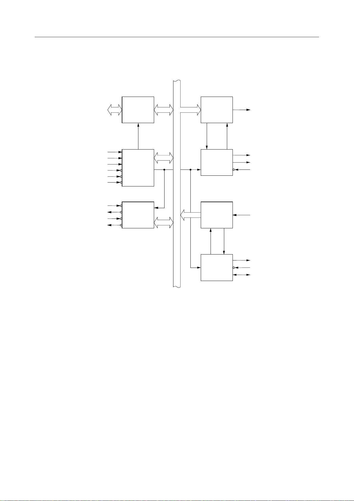
FUNCTIONAL BLOCK DIAGRAM
D
7 - D0
RESET
CLK
C/D
RD
WR
DSR
DTR
CTS
RTS
CS
Data Bus
Buffer
Read/Write
Control
Logic
Modem
Control
Transmit
Buffer
(P - S)
Transmit
Control
Internal Bus Line
Recieve
Buffer
(S - P)
Recieve
Control
TXD
TXRDY
TXE
TXC
RXD
RXRDY
RXC
SYNDET/BD
2/26
¡ Semiconductor MSM82C51A-2RS/GS/JS
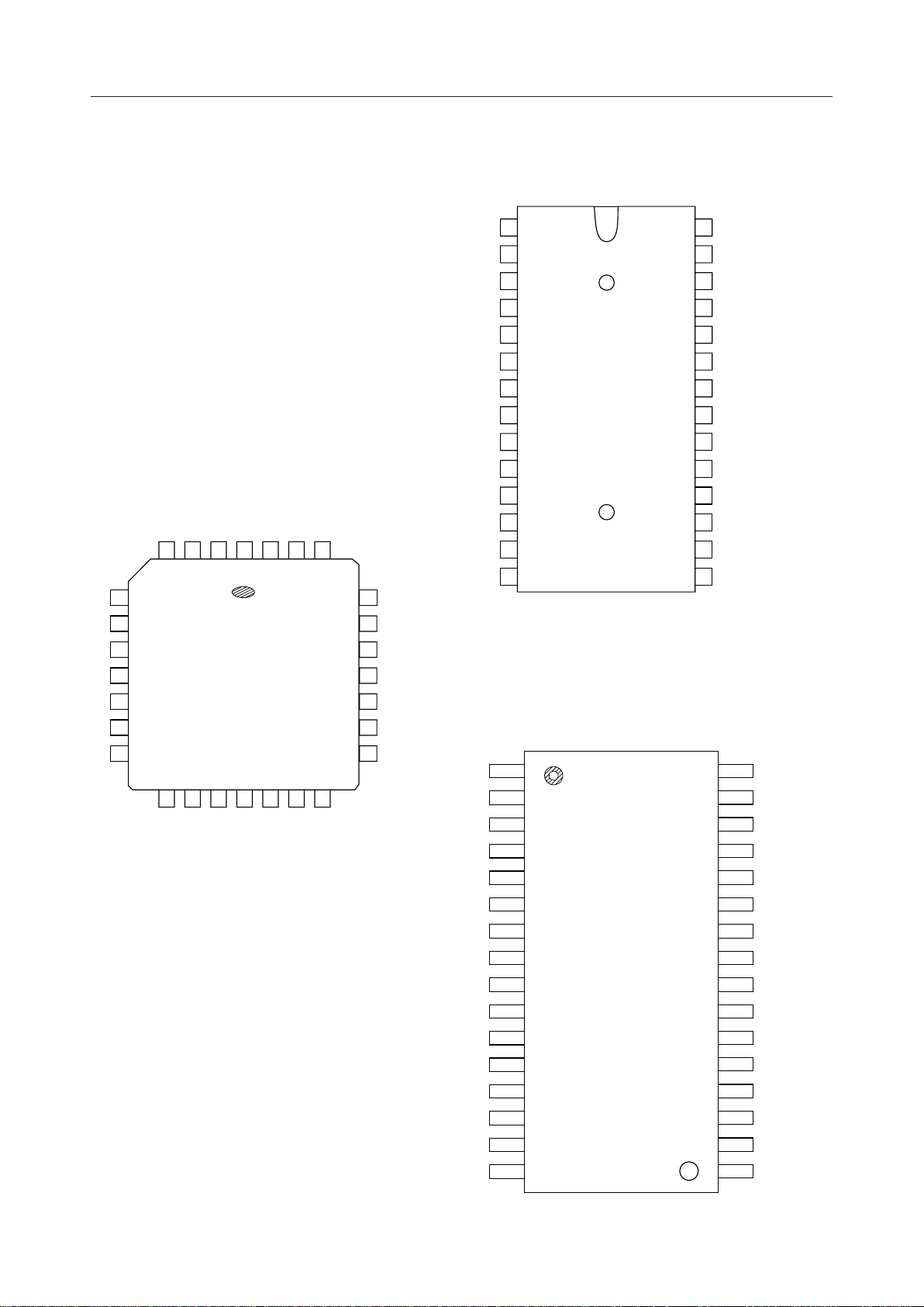
PIN CONFIGURATION (TOP VIEW)
28 pin Plastic DIP
D
D
D
D
TXC
WR
CS
D
1
2
D
2
3
RXD
3
GND
4
D
5
4
D
6
5
D
7
6
8
D
7
9
TXC
10
RXRDY
RXD
NC
GND
TXC
WR
C/D
RXRDY
D
D
D
D
D
D
CS
NC
RD
WR
CS
C/D
RD
2
3
4
5
6
7
11
12
13
14
32 pin Plastic SSOP
1
2
3
4
5
6
7
8
9
10
11
12
13
14
15
16
28 pin Plastic QFJ
RXD
3
3D2D1
D
2
1
GND
4
5
4
6
5
7
6
8
7
9
10
11
12
13
14
15
RD
C/D
TXRDY
RXRDY
0
CC
D
V
28
27
26
16
17
18
CTS
SYNDET/BD
TXEMPTY
25
24
23
22
21
20
19
RXC
DTR
RTS
DSR
RESET
CLK
TXD
28
D
D
27
26
V
25
RXC
24
DTR
23
RTS
22
DSR
RESET
21
20
CLK
TXD
19
TXEMPTY
18
CTS
17
SYNDET/BD
16
TXRDY
15
1
0
CC
32
31
30
29
28
27
26
25
24
23
22
21
20
19
18
17
D
1
D
0
V
CC
NC
RXC
DTR
RTS
DSR
RESET
CLK
TXD
TXEMPTY
NC
CTS
SYNDET/BD
TXRDY
3/26
¡ Semiconductor MSM82C51A-2RS/GS/JS
FUNCTION
Outline
The MSM82C51A-2's functional configuration is programed by software.
Operation between the MSM82C51A-2 and a CPU is executed by program control. Table 1
shows the operation between a CPU and the device.
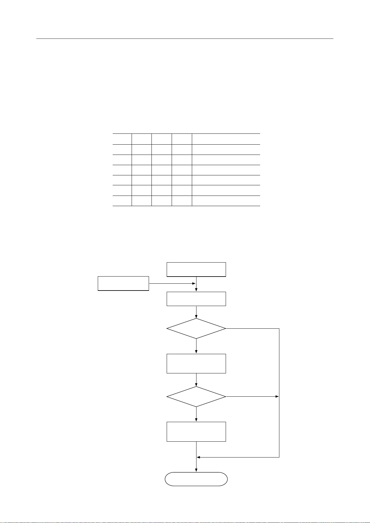
Table 1 Operation between MSM82C51A and CPU
CS
C/D
1
0
0
0
0
0
RD
¥
¥
1
1
0
0
WR
¥
1
0
1
0
1
¥
1
1
0
1
0
Data Bus 3-State
Data Bus 3-State
Status Æ CPU
Control Word ¨ CPU
Data Æ CPU
Data ¨ CPU
It is necessary to execute a function-setting sequence after resetting the MSM82C51A-2. Fig. 1
shows the function-setting sequence.
If the function was set, the device is ready to receive a command, thus enabling the transfer of
data by setting a necessary command, reading a status and reading/writing data.
External Reset
Internal Reset
Write Mode Instruction
Asynchronous
no
Write First Sync
Charactor
Single
Sync Mode
no
Write Second Sync
Charactor
End of Mode Setting
yes
yes
Fig. 1 Function-setting Sequence (Mode Instruction Sequence)
4/26
¡ Semiconductor MSM82C51A-2RS/GS/JS
)
Control Words
There are two types of control word.
1. Mode instruction (setting of function)
2. Command (setting of operation)
1) Mode Instruction
Mode instruction is used for setting the function of the MSM82C51A-2. Mode instruction
will be in “wait for write” at either internal reset or external reset. That is, the writing of a
control word after resetting will be recognized as a “mode instruction.”
Items set by mode instruction are as follows:
• Synchronous/asynchronous mode
• Stop bit length (asynchronous mode)
• Character length
• Parity bit
• Baud rate factor (asynchronous mode)
• Internal/external synchronization (synchronous mode)
• Number of synchronous characters (Synchronous mode)
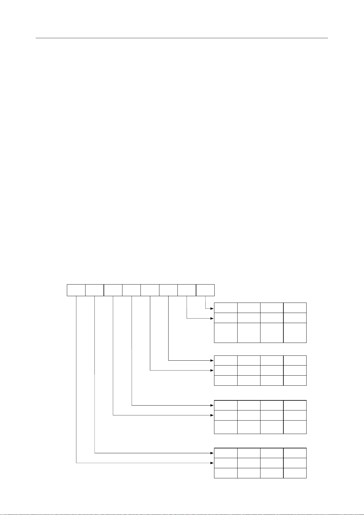
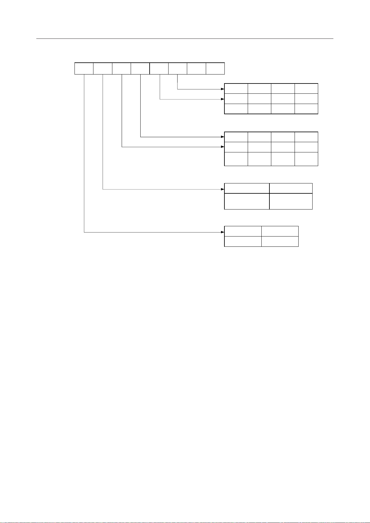
The bit configuration of mode instruction is shown in Figures 2 and 3. In the case of
synchronous mode, it is necessary to write one-or two byte sync characters.
If sync characters were written, a function will be set because the writing of sync characters
constitutes part of mode instruction.
D
S
D
7
1
6
S
1
D
EP PEN L
D
5
D
4
D
3
2
D
2
L
B
1
D
1
0
B
2
1
Baud Rate Factor
0 1 0 1
0 0 1 1
Refer to
Fig. 3
SYNC
0 1 0
0 0 1
5 bits 6 bits 7 bits
0 1 0 1
0 0 1 1
Disable
1 ¥ 16 ¥ 64 ¥
Charactor Length
Odd
Parity
Parity Check
Disable
1
1
8 bits
Even
Parity
Stop bit Length
0 1 0
0 0 1
Inhabit 1 bit 1.5
bits
Fig. 2 Bit Configuration of Mode Instruction (Asynchronous
1
1
2 bits
5/26
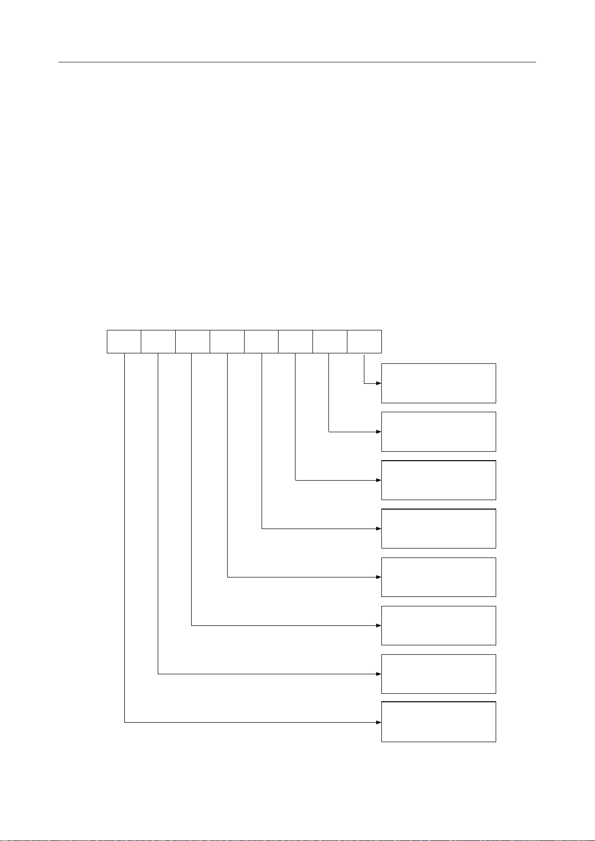
¡ Semiconductor MSM82C51A-2RS/GS/JS
)
D
D
7
SCS ESD EP PEN L
D
6
D
5
D
4
D
3
2
D
2
L
1
1
0 0
D
0
Charactor Length
0 1 0
0 0 1
5 bits 6 bits 7 bits
1
1
8 bits
Parity
0 1 0 1
0 0 1 1
Disable
Odd
Parity
Disable
Even
Parity
Synchronous Mode
0 1
Internal
Synchronization
External
Synchronization
Number of Synchronous Charactors
0 1
2 Charactors 1 Charactor
Fig. 3 Bit Configuration of Mode Instruction (Synchronous
6/26
¡ Semiconductor MSM82C51A-2RS/GS/JS
g
2) Command
Command is used for setting the operation of the MSM82C51A-2.
It is possible to write a command whenever necessary after writing a mode instruction and
sync characters.
Items to be set by command are as follows:
• Transmit Enable/Disable
• Receive Enable/Disable
• DTR, RTS Output of data.
• Resetting of error flag.
• Sending to break characters
• Internal resetting
• Hunt mode (synchronous mode)
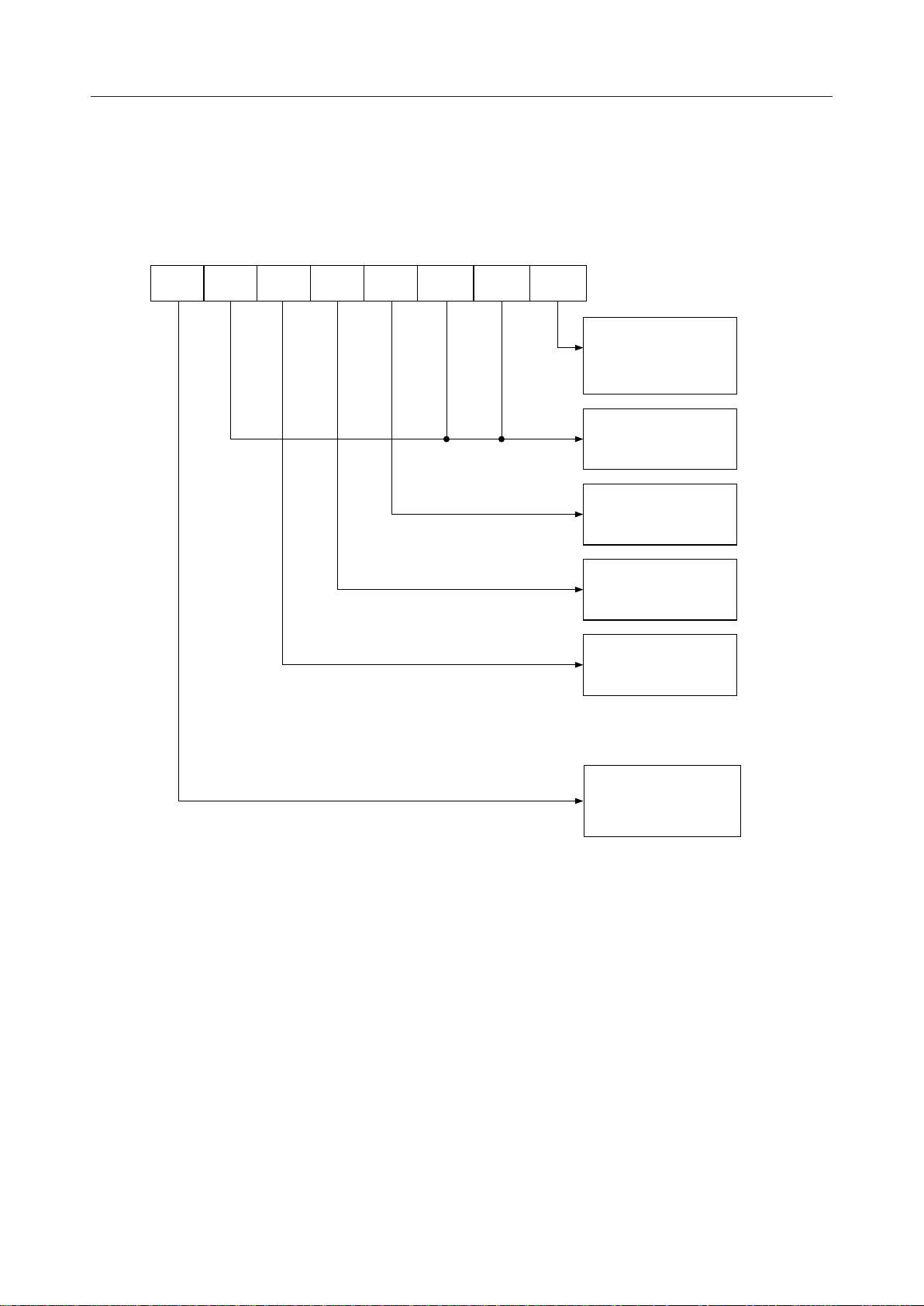
The bit configuration of a command is shown in Fig. 4.
D
EH
D
7
IR
D
6
RTS
D
5
ER
D
4
SBRK
D
3
RXE
D
2
DTR
D
1
0
TXEN
1ºTransmit Enable
0ºDisable
DTR
1 Æ DTR = 0
0 Æ DTR = 1
1ºRecieve Enable
0ºDisable
1ºSent Break Charactor
0ºNormal Operation
1ºReset Error Flag
0ºNormal Operation
RTS
1 Æ RTS = 0
0 Æ RTS = 1
1ºInternal Reset
0ºNormal Operation
1ºHunt Mode (Note)
0ºNormal Operation
Note: Seach mode for synchronous
charactors in synchronous mode.
. 4 Bit Configuration of Command
Fi
7/26
¡ Semiconductor MSM82C51A-2RS/GS/JS
g
Status Word
It is possible to see the internal status of MSM82C51A-2 by reading a status word.
The bit configuration of status word is shown in Fig. 5.
D
DSR
D
7
SYNDET
/BD
D
6
FE
D
5
OE
D
4
PE
3
D
2
TXEMPTY
D
1
RXRDY
D
0
TXRDY
Parity Different from
TXRDY Terminal.
Refer to "Explanation"
of TXRDY Terminals.
Same as terminal.
Refer to "Explanation"
of Terminals.
1ºParity Error
1ºOverrun Error
1ºFraming Error
Note:
Only asynchronous mode.
Stop bit cannot be detected.
Shows Terminal DSR
1ºDSR = 0
0ºDSR = 1
Fi
. 5 Bit Configuration of Status Word
Standby Status
It is possible to put the MSM82C51A-2 in “standby status”
When the following conditions have been satisfied the MSM82C51A-2 is in “standby status.”
(1) CS terminal is fixed at Vcc level.
(2) Input pins other CS , D0 to D7, RD, WR and C/D are fixed at Vcc or GND level (including
SYNDET in external synchronous mode).
Note: When all output currents are 0, ICCS specification is applied.
8/26

¡ Semiconductor MSM82C51A-2RS/GS/JS
Pin Description
D0 to D7 (l/O terminal)
This is bidirectional data bus which receive control words and transmits data from the CPU and
sends status words and received data to CPU.
RESET (Input terminal)
A “High” on this input forces the MSM82C51A-2 into “reset status.”
The device waits for the writing of “mode instruction.”
The min. reset width is six clock inputs during the operating status of CLK.
CLK (Input terminal)
CLK signal is used to generate internal device timing.
CLK signal is independent of RXC or TXC.
However, the frequency of CLK must be greater than 30 times the RXC and TXC at Synchronous
mode and Asynchronous “x1” mode, and must be greater than 5 times at Asynchronous “x16”
and “x64” mode.
WR (Input terminal)
This is the “active low” input terminal which receives a signal for writing transmit data and
control words from the CPU into the MSM82C51A-2.
RD (Input terminal)
This is the “active low” input terminal which receives a signal for reading receive data and
status words from the MSM82C51A-2.
C/D (Input terminal)
This is an input terminal which receives a signal for selecting data or command words and status
words when the MSM82C51A-2 is accessed by the CPU.
If C/D = low, data will be accessed.
If C/D = high, command word or status word will be accessed.
CS (Input terminal)
This is the “active low” input terminal which selects the MSM82C51A-2 at low level when the
CPU accesses.
Note: The device won’t be in “standby status”; only setting CS = High.
Refer to “Explanation of Standby Status.”
TXD (output terminal)
This is an output terminal for transmitting data from which serial-converted data is sent out.
The device is in “mark status” (high level) after resetting or during a status when transmit is
disabled. It is also possible to set the device in “break status” (low level) by a command.
9/26

¡ Semiconductor MSM82C51A-2RS/GS/JS
TXRDY (output terminal)
This is an output terminal which indicates that the MSM82C51A-2 is ready to accept a
transmitted data character. But the terminal is always at low level if CTS = high or the device
was set in “TX disable status” by a command.
Note: TXRDY status word indicates that transmit data character is receivable,
regardless
of CTS or command.
If the CPU writes a data character, TXRDY will be reset by the leading edge or WR
signal.
TXEMPTY (Output terminal)
This is an output terminal which indicates that the MSM82C51A-2 has transmitted all the
characters and had no data character.
In “synchronous mode,” the terminal is at high level, if transmit data characters are no longer
remaining and sync characters are automatically transmitted. If the CPU writes a data
character, TXEMPTY will be reset by the leading edge of WR signal.
Note : As the transmitter is disabled by setting CTS “High” or command, data written
before disable will be sent out. Then TXD and TXEMPTY will be “High”.
Even if a data is written after disable, that data is not sent out and TXE will be
“High”.After the transmitter is enabled, it sent out. (Refer to Timing Chart of
Transmitter Control and Flag Timing)
TXC (Input terminal)
This is a clock input signal which determines the transfer speed of transmitted data.
In “synchronous mode,” the baud rate will be the same as the frequency of TXC.
In “asynchronous mode”, it is possible to select the baud rate factor by mode instruction.
It can be 1, 1/16 or 1/64 the TXC.
The falling edge of TXC sifts the serial data out of the MSM82C51A-2.
RXD (input terminal)
This is a terminal which receives serial data.
RXRDY (Output terminal)
This is a terminal which indicates that the MSM82C51A-2 contains a character that is ready to
READ.
If the CPU reads a data character, RXRDY will be reset by the leading edge of RD signal.
Unless the CPU reads a data character before the next one is received completely, the preceding
data will be lost. In such a case, an overrun error flag status word will be set.
RXC (Input terminal)
This is a clock input signal which determines the transfer speed of received data.
In “synchronous mode,” the baud rate is the same as the frequency of RXC.
In “asynchronous mode,” it is possible to select the baud rate factor by mode instruction.
It can be 1, 1/16, 1/64 the RXC.
10/26

¡ Semiconductor MSM82C51A-2RS/GS/JS
SYNDET/BD (Input or output terminal)
This is a terminal whose function changes according to mode.
In “internal synchronous mode.” this terminal is at high level, if sync characters are received and
synchronized. If a status word is read, the terminal will be reset.
In “external synchronous mode, “this is an input terminal.
A “High” on this input forces the MSM82C51A-2 to start receiving data characters.
In “asynchronous mode,” this is an output terminal which generates “high level”output upon
the detection of a “break” character if receiver data contains a “low-level” space between the
stop bits of two continuous characters. The terminal will be reset, if RXD is at high level.
After Reset is active, the terminal will be output at low level.
DSR (Input terminal)
This is an input port for MODEM interface. The input status of the terminal can be recognized
by the CPU reading status words.
DTR (Output terminal)
This is an output port for MODEM interface. It is possible to set the status of DTR by a command.
CTS (Input terminal)
This is an input terminal for MODEM interface which is used for controlling a transmit circuit.
The terminal controls data transmission if the device is set in “TX Enable” status by a command.
Data is transmitable if the terminal is at low level.
RTS (Output terminal)
This is an output port for MODEM interface. It is possible to set the status RTS by a command.
11/26

¡ Semiconductor MSM82C51A-2RS/GS/JS
ABSOLUTE MAXIMUM RATING
Parameter Unit
Power Supply Voltage
Input Voltage
Output Voltage
Storage Temperature
Power Dissipation
Symbol
V
CC
V
IN
V
OUT
T
STG
P
D
MSM82C51A-2RS
MSM82C51A-2GS MSM82C51A-2JS
–0.5 to +7
–0.5 to V
–0.5 to V
CC
CC
+0.5
+0.5
–55 to +150
0.7
0.90.9
OPERATING RANGE
Rating
Parameter UnitSymbol
Power Supply Voltage
Operating Temperature
V
CC
T
op
Range
3 - 6
–40 to 85
RECOMMENDED OPERATING CONDITIONS
Parameter UnitSymbol
Power Supply Voltage
Operating Temperature
"L" Input Voltage V
"H" Input Voltage
V
CC
T
op
IL
V
IH
Min.
4.5
–40
–0.3
2.2
Typ.
5V
+25
—
—
Max.
+85
+0.8
V
CC
5.5
V
V
V
°C
W
+0.3
Conditions
With respect
to GND
—
Ta = 25°C
V
°C
°C
V
V
DC CHARACTERISTICS
Parameter Unit
"L" Output Voltage
"H" Output Voltage
Input Leak Current
Output Leak Current
Operating Supply
Current
Standby Supply
Current
Symbol
V
OL
V
OH
I
LI
I
LO
I
CCO
I
CCS
Min.
—
3.7
–10
–10
—
—
Typ. Max.
— 0.45 V
——V
—10mA
—10mA
—5mA
— 100 mA
(V
= 4.5 to 5.5 V Ta = –40°C to +85°C)
CC
Measurement Conditions
I
= 2.5 mA
OL
I
= –2.5 mA
OH
IN
OUT
£ V
£ V
CC
CC
0 £ V
0 £ V
Asynchronous X64 during Transmitting/
Receiving
All Input voltage shall be fixed at V
CC
or
GND level.
12/26

¡ Semiconductor MSM82C51A-2RS/GS/JS
AC CHARACTERISTICS
CPU Bus Interface Part
(VCC = 4.5 to 5.5 V, Ta = –40 to 85°C)
Parameter UnitSymbol
Address Stable before RD t
Address Hold Time for RD t
RD Pulse Width t
Data Delay from RD
RD to Data Float
Recovery Time between RD t
Address Stable before WR t
Address Hold Time for WR
WR Pulse Width
Data Set-up Time for WR t
Data Hold Time for WR t
Recovery Time between WR
RESET Pulse Width
t
AR
RA
RR
t
RD
t
DF
RVR
AW
t
WA
t
WW
DW
WD
t
RVW
RESW
Min.
20
20
130
6
20
100
0
6
6
Max.
—
—
—
100
75
—
—
—
—
—
—
—
—
t
t
t
ns
ns
ns
ns—
ns10
CY
ns
ns20
ns100
ns
ns
CY
CY
Remarks
Note 2
Note 2
—
—
—
Note 5
Note 2
Note 2
—
—
—
Note 4
—
13/26

¡ Semiconductor MSM82C51A-2RS/GS/JS
Serial Interface Part
Parameter UnitSymbol
Main Clock Period t
Clock Low Tme t
Clock High Time t
Clock Rise/Fall Time
TXD Delay from Falling Edge of TXC
1 ¥ Baud
Transmitter Clock Frequency
Transmitter Clock Low Time
Transmitter Clock High Time
Receiver Clock Frequency
Receiver Clock Low Time
Receiver Clock High Time
Time from the Center of Last Bit to the Rise of
TXRDY
Time from the Leading Edge of WR to the Fall
of TXRDY
16 ¥ Baud
64 ¥ Baud
1 ¥ Baud
16 ¥, 64 ¥ Baud
1 ¥ Baud
16 ¥ Baud
64 ¥ Baud
1 ¥ Baud
16 ¥, 64 ¥ Baud
1 ¥ Baud
16 ¥, 64 ¥ Baud
t
t
TXRDY CLEAR
CY
f
f
t
r, tf
t
DTX
f
TX
f
TX
f
TX
t
TPW
t
TPW
t
TPD
t
TPD
f
RX
f
RX
f
RX
t
RPW
t
RPW
t
RPD
t
RPD
TXRDY
Min.
160
50
70
DC
DC
13
2
15
316 ¥, 64 ¥ Baud
DC
DC
13
2
15
3
—
= 4.5 to 5.5 V, Ta = –40 to 85°C)
(V
CC
Max.
—
—
tCY –50
20
1
64
615
615
—
—
—
—
64DC
615
615
—
—
—
—
8
400
ns
ns
ns
ns—
mS—
kHz
kHz
kHzDC
t
t
t
t
kHz1 ¥ Baud
kHz
kHz
t
t
t
t
t
ns—
Remarks
CY
CY
CY
CY
CY
CY
CY
CY
CY
Note 3
—
—
—
—
Note 3
—
—
—
—
Note 3
—
—
—
—
—
—
Time From the Center of Last Bit to the Rise of RXRDY
Time from the Leading Edge of RD to the Fall
of RXRDY
t
t
RXRDY CLEAR
Internal SYNDET Delay Time from Rising Edge of RXC
SYNDET Setup Time for RXC t
TXE Delay Time from the Center of Last Bit t
TXEMPTY
MODEM Control Signal Delay Time from Rising Edge
of WR
MODEM Control Signal Setup Time for Falling Edge
of RD
RXD Setup Time for Rising Edge of RXC (1X Baud)
RXD Hold Time for Falling Edge of RXC (1X Baud)
t
t
RXRDY
t
IS
ES
t
WC
t
CR
RXDS
RXDH
—
—
18
20
8
20
11
17
26
400
26
—
—
—
—
—
—
t
CY
ns—
t
CY
t
CY
t
CY
t
CY
t
CY
t
CY
t
CY
—
—
—
—
—
—
—
—
—
Notes: 1. AC characteristics are measured at 150 pF capacity load as an output load based on 0.8 V at
low level and 2.2 V at high level for output and 1.5 V for input.
2. Addresses are CS and C/D.
3. fTX or fRX £ 1/(30 Tcy) 1¥ Baud
f
or fRX £ 1/(5 Tcy) 16¥, 64¥ Baud
TX
4. This recovery time is mode Initialization only. Recovery time between command writes for
Asynchronous Mode is 8 t
and for Synchronous Mode is 18 tCY.
CY
Write Data is allowed only when TXRDY = 1.
5. This recovery time is Status read only.
Read Data is allowed only when RXRDY = 1.
6. Status update can have a maximum delay of 28 clock periods from event affecting the status.
14/26

¡ Semiconductor MSM82C51A-2RS/GS/JS
TIMING CHART
Sytem Clock Input
CLK
Transmitter Clock and Data
t
TXC (1 ¥ MODE)
TPW
TXC (16 ¥ MODE)
t
DTX
TXD
Receiver Clock and Data
t
t
t
f
r
f
t
TPD
t
DTX
t
f
t
CY
RXD
RXC (1 ¥ Mode)
RXC (16 ¥ Mode)
INT Sampling
Pulse
(RXBAUD Counter starts here)
Start bit
t
t
RPW
8RXC Periods
(16¥Mode)
RPD
16 RXC Periods (16 ¥ Mode)
3t
CY
t
f
Data bit Data bit
3t
CY
15/26

¡ Semiconductor MSM82C51A-2RS/GS/JS
Write Data Cycle (CPU Æ USART)
TXRDY
t
TXRDY Clear
t
WR
Don't Care Don't Care
DATA IN (D. B.)
WW
t
DW
Data Stable
t
WD
t
C/D
CS
AW
t
AW
Read Data Cycle (CPU ¨ USART)
RXRDY
RD
DATA OUT (D. B.)
C/D
CS
Data Float Data Float
t
AR
t
AR
Write Control or Output Port Cycle (CPU Æ USART)
t
RXRDY Clear
t
RR
t
RD
Data Out Active
t
t
WA
WA
t
DF
t
RA
t
RA
DTR. RTS
WR
DATA IN
(D. B.)
C/D
CS
Don't Care
t
t
AW
AW
Read Control or Input Port Cycle (CPU ¨ USART)
DSR. CTS
t
CR
RD
DATA OUT
(D. B.)
C/D
CS
Data Float
t
AR
t
AR
t
WW
t
DW
Data Stable
Data Out Active
t
WC
t
WD
Don't Care
t
WA
t
WA
t
RR
t
t
RA
t
RA
DF
Data Float
t
RD
16/26

¡ Semiconductor MSM82C51A-2RS/GS/JS
Transmitter Control and Flag Timing (ASYNC Mode)
CTS
TXEMPTY
TXRDY
(STATUS BIT)
t
TXRDY
TXRDY
(PIN)
C/D
Wr DATA 1 Wr DATA 2 Wr DATA 3 Wr DATA 4
Wr TxEn
WR
TXD
DATA CHAR 1 DATA CHAR 2 DATA CHAR 3 DATA CHAR 4
Note: The wave-form chart is based on the case of 7-bit data length + parity bit + 2 stop bit.
Receiver Control and Flag Timing (ASYNC Mode)
BREAK DETECT
FRAMING ERROR
(Status Bit)
OVERRUN ERROR
(Status Bit)
RXRDY
C/D
WR
RD
RXDATA
Wr RxEn
t
RXRDY
Data CHAR 1 Data CHAR 2 Data CHAR 3
DATA
CHAR2
Lost
Rd Data
Wr Error
Break
t
TXEMPTY
RxEn Err Res
Wr SBRK
0123456
START BIT
RxEn
STOP BIT
Data Bit
Start Bit
Stop Bit
Parity Bit
Note: The wave-form chart is based on the case of 7 data bit length + parity bit + 2 stop bit.
Transmitter Control and Flag Timing (SYNC Mode)
CTS
TXEMPTY
TXRDY
(StatusBit)
TXRDY (Pin)
C/D
WR
Marking State
TXD
Note: The wave-form chart is based on the case of 5 data bit length + parity bit and 2 synchronous charactors.
Wr Data
Wr Data
CHAR2
CHAR1
Data
CHAR1
01234 01234 01234
Data
CHAR2
Wr Data
CHAR3
SYNC
CHAR1
Wr Data
CHAR4
SYNC
SYNC CHAR2
CHAR3
01234 01234 0 123 4
Data
CHAR4
Wr Commond
SBRK
Marking
State
Spacing
State
Wr Data
CHAR5
Marking
State
Data
CHAR5
01234 01234 01
SYNC
CHAR ETC
PARPARPARPARPARPARPARPAR
17/26

¡ Semiconductor MSM82C51A-2RS/GS/JS
y
Receiver Control and Flag Timing (SYNC Mode)
SYNDET
(Pin) (Note 1)
SYNDET (SB)
OVERRUN
ERROR (SB)
RXRDY (PIN)
Note:
(Note 2)
t
t
IS
Data
CHAR2
Lost
C/D
Wr EH
RxEn
WR
RD
Don't
Care
x x x x x x 0 1 2 3 4 0 1 2 3 4 0 1 2 3 4 0 1 2 3 4 0 1 2 3 4 0 1 2 3 4 0 1 2 3 4 x x x x x x x 0 1 2 3 4 0 1 x 3 4
RXD
RXC
SYNC
CHAR 1
SYNC
Data
CHAR 2
CHAR 1
PAR PAR PAR PAR PAR PAR PAR PAR PAR PAR
CHAR ASSY Begins
Exit Hunt Mode
Set SYNDET
Rd Status Wr Err Res
Rd Data
CHAR 1
Data
CHAR 2
Data
CHAR 3
Rd Data
CHAR 3
SYNC
CHAR 1
Rd SYNC
CHAR 1
SYNC
CHAR 2
Exit Hunt Mode
Set SYNDET (Status bit)
ES
Rd Status
Wr EH
o
Don't Care
Rd Status
Data
CHAR 1
Data
CHAR 2
CHAR ASSY
Begins
Set SYNDET (Status bit)
ETC
1. Internal Synchronization is based on the case of 5 data bit length + parity bit and 2 synchronous charactor.
2. External S
nchronization is based on the case of 5 data bit length + parity bit.
Note: 1. Half-bit processing for the start bit
When the MSM82C51A-2 is used in the asynchronous mode, some problems are
caused in the processing for the start bit whose length is smaller than the 1-data bit
length. (See Fig. 1.)
Start bit Length Mode
Smaller than 7-Receiver Clock Length ¥16
Smaller than 31-Receiver Clock Length ¥64
8-Receiver Clock Length ¥16
32-Receiver Clock Length
9 to 16-Receiver Clock Length
¥64 Data cannot be received correctly due to a malfunction.
¥16 The bit is regarded as a start bit. (normal)
The short start bit is ignored. (Normal)
The short start bit is ignored. (Normal)
Data cannot be received correctly due to a malfunction.
33 to 64-Receiver Clock Length ¥64 The bit is regarded as a start bit. (normal)
Operation
2. Parity flag after a break signal is received (See Fig. 2.)
When the MSM82C51A-2 is used in the asynchrous mode, a parity flag may be set
when the next normal data is read after a break signal is received.
A parity flag is set when the rising edge of the break signal (end of the break signal)
is changed between the final data bit and the parity bit, through a RXRDY signal may
not be outputted.
If this occurs, the parity flag is left set when the next normal dats is received, and the
received data seems to be a parity error.
18/26

¡ Semiconductor MSM82C51A-2RS/GS/JS
Half-bit Processing Timing Chart for the Start bit (Fig. 1)
Normal Operation
RXD
ST D0D1D2D3D4D5D6D7PSP STD0D1D2D3D4D5D6D7PSP
RXRDY
The Start bit Is Shorter Than a 1/2 Data bit
ST D
RXD
0D1D2D3D4D5D6D7
ST
RXRDY
The Start bit Is a 1/2 Data bit (A problem of MSM82C51A-2)
ST D
RXD
0D1D2D3D4D5D6D7
ST
RXRDY
PSP
PSP
The Start bit Is Longer Than a 1/2 Data bit
RXD
ST
RXRDY
- D7:
0
Start bit
Stop bit
Parity bit
Data bits
ST:
SP:
P:
D
A RXRDY signal is outputted during data
reception due to a malfunction.
ST D
0D1D2D3D4D5D6D7
PSP
19/26

¡ Semiconductor MSM82C51A-2RS/GS/JS
p
Break Signal Reception Timing and Parity Flag (Fig. 2)
Normal Operation
ST D
0
RXD
RXRDY
Bug Timing
ST D
0
RXD
RXRDY
Normal Operation
D7P SP ST D
D7P SP ST D
D7P SP ST D0D1D2D3D4D5D6D7PBIT POS.
0
SP
≠
No parity flag is set. and no RXRDY signal
is outputted.
D7P SP ST D0D1D2D3D4D5D6D7PBIT POS.
0
SP
≠
A parity flag is set, but, no RXRDYsignal
is outputted.
RXD
RXRDY
ST D
D7P SP ST D
0
D7P SP ST D0D1D2D3D4D5D6D7PBIT POS.
0
SP
≠
A parity flag is set. and a RXRDY signal
is out
utted.
20/26

¡ Semiconductor MSM82C51A-2RS/GS/JS
NOTICE ON REPLACING LOW-SPEED DEVICES WITH HIGH-SPEED DEVICES
The conventional low speed devices are replaced by high-speed devices as shown below.
When you want to replace your low speed devices with high-speed devices, read the replacement
notice given on the next pages.
High-speed device (New)
M80C85AH
M80C86A-10
M80C88A-10
M82C84A-2
M81C55-5
M82C37B-5
M82C51A-2
M82C53-2
M82C55A-2
Low-speed device (Old)
M80C85A/M80C85A-2
M80C86A/M80C86A-2
M80C88A/M80C88A-2
M82C84A/M82C84A-5
M81C55
M82C37A/M82C37A-5
M82C51A
M82C53-5
M82C55A-5
Remarks
8bit MPU
16bit MPU
8bit MPU
Clock generator
RAM.I/O, timer
DMA controller
USART
Timer
PPI
21/26

¡ Semiconductor MSM82C51A-2RS/GS/JS
Differences between MSM82C51A and MSM82C51A-2
1) Manufacturing Process
These devices use a 3 m Si-Gate CMOS process technology and have the same chip size.
2) Function
These devices have the same logics except for changes in AC characteristics listed in (3-2).
3) Electrical Characteristics
3-1) DC Characteristics
Parameter
measurement conditions +2.0 mA +2.5 mA
V
OL
measurement conditions -400 mA -2.5 mA
V
OH
Symbol
I
OL
I
OH
MSM82C51A MSM82C51A-2
Although the output voltage characteristics of these devices are identical, but the measurement
conditions of the MSM82C51A-2 are more restricted than the MSM82C51A.
3-2) AC Characteristics
Parameter
RD Pulse Width 250 ns minimum 130 ns minimum
RD Rising to Data Difinition 200 ns maximum 100 ns maximum
RD Rising to Data Float 100 ns maximum 75 ns minimum
WR Pulse Width 250 ns minimum 100 ns minimum
Data Setup Time for WR Rising
Symbol
t
RR
t
RD
t
RF
t
WW
t
DW
MSM82C51A MSM82C51A-2
150 ns minimum 100 ns minimum
t
Data Hold Time for WR Rising 20 ns minimum 0 ns minimum
Master Clock Period 250 ns minimum 160 ns minimum
Clock Low Time 90 ns minimum 50 ns minimum
Clock High Time
WD
t
CY
t
t
f
f
120 ns minimum
t
90 ns maximum
CY-
70 ns minimum
t
50 ns maximum
CY-
As shown above, the MSM82C51A-2 satisfies the characteristics of the MSM82C51A.
22/26

¡ Semiconductor MSM82C51A-2RS/GS/JS
PACKAGE DIMENSIONS
(Unit : mm)
DIP28-P-600-2.54
Package material
Lead frame material
Pin treatment
Solder plate thickness
Package weight (g)
Epoxy resin
42 alloy
Solder plating
5 mm or more
4.30 TYP.
Notes for Mounting the Surface Mount Type Package
The SOP, QFP, TSOP, SOJ, QFJ (PLCC), SHP and BGA are surface mount type packages, which
are very susceptible to heat in reflow mounting and humidity absorbed in storage.
Therefore, before you perform reflow mounting, contact Oki’s responsible sales person for the
product name, package name, pin number, package code and desired mounting conditions
(reflow method, temperature and times).
23/26

¡ Semiconductor MSM82C51A-2RS/GS/JS
(Unit : mm)
QFJ28-P-S450-1.27
Spherical surface
Package material
Lead frame material
Pin treatment
Solder plate thickness
Package weight (g)
Epoxy resin
Cu alloy
Solder plating
5 mm or more
1.00 TYP.
Notes for Mounting the Surface Mount Type Package
The SOP, QFP, TSOP, SOJ, QFJ (PLCC), SHP and BGA are surface mount type packages, which
are very susceptible to heat in reflow mounting and humidity absorbed in storage.
Therefore, before you perform reflow mounting, contact Oki’s responsible sales person for the
product name, package name, pin number, package code and desired mounting conditions
(reflow method, temperature and times).
24/26

¡ Semiconductor MSM82C51A-2RS/GS/JS
(Unit : mm)
SSOP32-P-430-1.00-K
Mirror finish
Package material
Lead frame material
Pin treatment
Solder plate thickness
Package weight (g)
Epoxy resin
42 alloy
Solder plating
5 mm or more
0.60 TYP.
Notes for Mounting the Surface Mount Type Package
The SOP, QFP, TSOP, SOJ, QFJ (PLCC), SHP and BGA are surface mount type packages, which
are very susceptible to heat in reflow mounting and humidity absorbed in storage.
Therefore, before you perform reflow mounting, contact Oki’s responsible sales person for the
product name, package name, pin number, package code and desired mounting conditions
(reflow method, temperature and times).
25/26

¡ Semiconductor MSM82C51A-2RS/GS/JS
4) Notices on use
Note the following when replacing devices as the ASYNC pin is differently treated between the
MSM82C84A and the MSM82C84A-5/MSM82C84A-2:
Case 1: When only a pullup resistor is externally connected to.
The MSM82C84A can be replaced by the MSM82C84A-2.
Case 2: When only pulldown resistor is externally connected to.
When the pulldown resistor is 8 kiloohms or less, the MSM82C84A can be replaced by the
MSM82C84A-2.
When the pulldown resistor is greater than 8 kiloohms, use a pulldown resistor of 8 kiloohms or less.
Case 3: When an output of the other IC device is connected to the device.
The MSM82C84A can be replaced by the MSM82C84A-2 when the I
ASYNC pin of the MSM82C84A-2 has an allowance of 100 mA or more.
pin of the device to drive the
OL
26/26
 Loading...