

Page 1

查询MSM6679A-110供应商
MSM6679A-110
Voice Recognition Processor
Page 2

MSM6679A-110 Voice Recognition Processor ¡ Semiconductor
Contents
Description .......................................................................................................................................... 1
Features................................................................................................................................................ 1
Functional and I/O Diagrams .......................................................................................................... 2
Pin Descriptions ................................................................................................................................. 8
Electrical Specifications ..................................................................................................................... 12
Absolute Maximum Ratings ............................................................................................ 12
Operating Conditions ....................................................................................................... 12
DC Characteristics (VDD = 4.5 to 5.5 V, Ta = -40 to 80˚C) .......................................... 13
AC Characteristics ............................................................................................................ 14
Timing Diagrams .............................................................................................................. 15
Functional Description ...................................................................................................................... 17
Voice Recognition ............................................................................................................. 17
SI Recognition ................................................................................................... 17
SD Recognition ................................................................................................. 20
Name Tag Recording ........................................................................................................ 20
Audio Input Interface ....................................................................................................... 21
Audio Output Interface .................................................................................................... 21
Memory Interface .............................................................................................................. 21
External Voice Synthesis Control ................................................................................... 24
Serial Interface ................................................................................................................... 25
MSM6679A-110 Slave-Mode API .................................................................................................... 26
Command Summary ........................................................................................................ 27
Command Descriptions ................................................................................................... 31
Asynchronous Serial Protocol Example ........................................................................ 44
2
Page 3

¡ Semiconductor MSM6679A-110 Voice Recognition Processor
¡ Semiconductor
MSM6679A-110
SI/SD Voice Recognizer, Recorder/Player, and Speech Synthesizer
GENERAL DESCRIPTION
The MSM6679A-110 Voice Recognition Processor (VRP) is a slave-mode device that performs
five func-tions: speaker-independent (SI) voice recognition, speaker-dependent (SD) voice
recognition, solid-state sound recording, sound playback, and speech synthesis. The highly
integrated device also provides an on-chip memory controller, Flash memory interface, analog
data conversion, Oki speech synthesizer interface, and pulse width modulation (PWM) sound
output.
For SI recognition, the MSM6679A-110 contains a vocabulary template in external memory.
Pretrained SI vocabularies eliminate the need for laborious training, as usually required by SD
products. The memory requirements are dependent on the size of the vocabulary. The MSM6679A110 can tolerate background noise, while providing high recognition accuracy. In its designated
operating environment, the device achieves a typical recognition accuracy of >95% (using an
Oki-defined test procedure).
For SD recognition, the MSM6679A-110 stores SD vocabulary templates, as defined by the user,
in external SRAM. The MSM6679A-110 can create SD vocabularies of up to 61 words each, with
each word using approximately 50 bytes.
In addition to providing voice recognition capabilities, the MSM6679A-110 integrates a solidstate recorder/player, speech synthesis functions, and a tone generator. ADPCM recording/
playback provides high quality sound and efficient memory utilization. The MSM6679A-110 can
respond to spoken com-mands, verbally or with tones, via an on-chip speech synthesizer and
tone generator. For larger speech-synthesis requirements, the MSM6679A-110 also provides a
glueless MSM665x control interface for off-chip speech synthesis.
The MSM6679A-110 can interface to any application or personal computer via a serial interface
through an open, device-independent serial mode API (SMAPI). To accelerate code development,
Oki supplies an evaluation kit, and assembly and C language programs for this product.
FEATURES
• SI recognition
- Up to 20 - 25 words in each vocabulary
- Multiple vocabulary support
• SD recognition
- Up to 61 words in each vocabulary
- Multiple vocabulary support
• Speech synthesis
- Up to 2.3-sec internal and 27.6-sec external
speech synthesis on-chip; sample looping
and concatenation allows even longer
phrases.
- On-chip controller for MSM665x speech
synthesizer
- Standard beep tone outputs
- Pulse code modualation (PCM) and
adaptive differential pulse code
modualation (ADPCM) voice or soundeffect output
• Speech capture and playback
- 28-kbps ADPCM speech compression
• Serial ASCII command interface
• 6944-Hz audio input sample rate for record
and playback
• 10-kHz sample rate for voice recognition
• 200-msec recognition latency
• Flexible memory mapping for EPROM,
FLASH, and SRAM
• 32-MHz operation
• Packages: 84-pin PLCC (QFJ84-P-S115) or
100-pin TQFP (TQFP100-P-1414-0.50-K)
1
Page 4
MSM6679A-110 Voice Recognition Processor ¡ Semiconductor
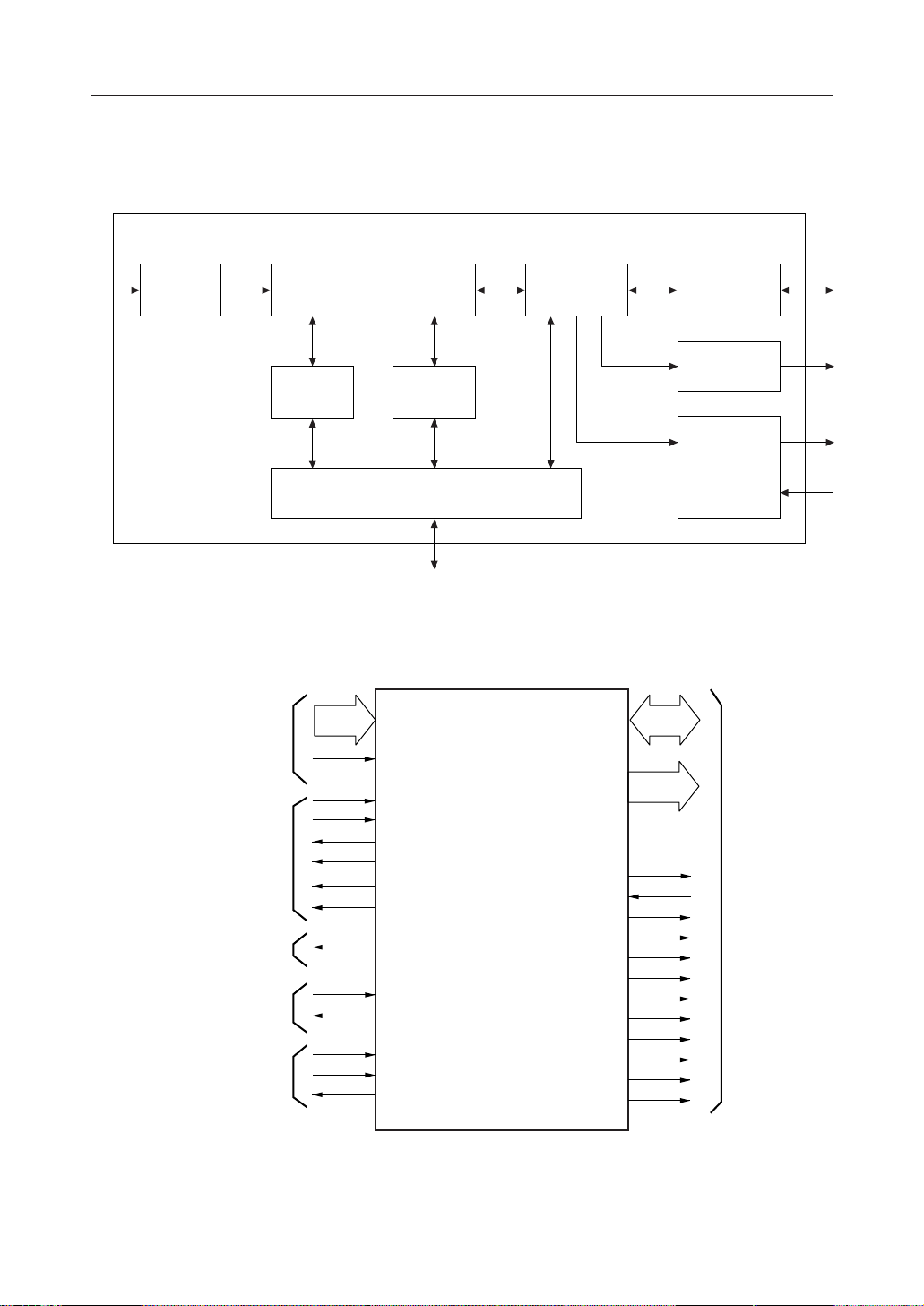
FUNCTIONAL AND I/O DIAGRAMS
Analog
Input
A/D Interface
Serial-Mode
MSM665x Interface
PWM Output
Serial Interface
IC Reset and Oscillator Inputs
Recognition and
Synthesis Engine
Vocabulary
Memory
Algorithm
Memory
External Memory Control
System
Controller
Figure 1. MSM6679A-110 Block Diagram
ADC0 ~ ADC9
VREF
NAR
BUSY
SI
SD
STROBE
RESOUT
VOICEOUT1
RXD1
TXD1
RES
OSC0
OSC1
AD0 ~ AD7
A8 ~ A15
ROMRD
WRRAM
RDRAM
LOADPGM
ROMPAGE0
ROMPAGE1
RAMPAGE0
RAMPAGE1
A15FLIP
EA
ALE
ES
Serial
Interface
PWM
Output
External
Speech
Synthesis
Control
Memory Interface
Figure 2. MSM6679A-110 Logic Symbol
2
Page 5
¡ Semiconductor MSM6679A-110 Voice Recognition Processor
N/C
N/C
N/C
N/C
N/C
N/C
RAMPAGE1
RAMPAGE0
LOADPGM
N/C
GNDSDSI
BUSY
N/C
ROMPAGE1
ROMPAGE0
STROBE
A15FLIP
N/C
N/C
747372717069686766656463626160595857565554
N/C
N/C
N/C
N/C
N/C
N/C+
RES
EA
V
DD
AV
DD
ADC0
ADC1
ADC2
ADC3
ADC4
ADC5
ADC6
ADC7
ADC8
ADC9
AGND
75
76
77
78
79
80
81
82
83
84
10
11
N/C
53
N/C
52
N/C–
51
A15
50
A14
49
A13
48
A12
47
A11
46
A10
45
A9
44
1
2
3
4
5
6
7
8
9
A8
43
V
42
DD
AD7
41
AD6
40
AD5
39
AD4
38
AD3
37
AD2
36
AD1
35
AD0
34
VOICEOUT1
33
121314151617181920212223242526272829303132
N/C+
VREF
N/C+
N/C
N/C
N/C
N/C
TXD1
RXD1
GND
OSC0
OSC1
ALE
ROMRD
RDRAM
WRRAM
N/C–
RESOUT
ES
NAR
N/C
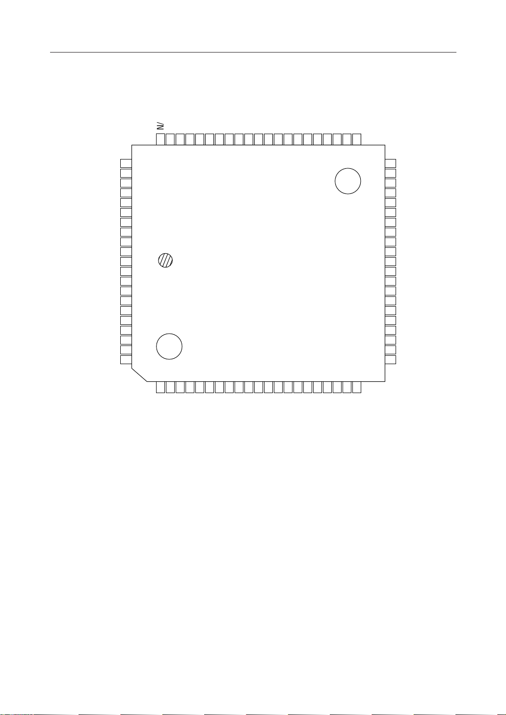
Figure 3. MSM6679A-110 84-Pin PLCC Pinout
3
Page 6

MSM6679A-110 Voice Recognition Processor ¡ Semiconductor
MSM6679A-110 Alphabetic Pin List
AD0
84-pin/
100-pin
34/28
Name
AD1 35/29
AD2 36/30
AD3 37/31
AD4 38/32
AD5 39/33
AD6 40/34
AD7 41/35
A8 43/39
A9 44/40
Name
84-pin/
100-pin
A10 45/41
A11 46/42
A12 47/43
A13 48/44
A14 49/45
A15 50/46
A15FLIP 56/54
ADC0 1/89
ADC1 2/90
ADC2 3/91
Name
84-pin/
100-pin
ADC3 4/92
ADC4 5/93
ADC5 6/94
ADC6 7/95
ADC7 8/96
ADC8 9/97
ADC9 10/98
AGND 11/99
ALE 24/16
AVDD 84/87
Name
84-pin/
100-pin
BUSY 61/60
13,14,80/3,4,82
N/C+
28,51/20,47
N/C–
EA 82/84
ES 30/22
GND
21,64/12,63
LOADPGM
66/66
Name
RAMPAGE0
RAMPAGE1
RDRAM 27/19
RESOUT 29/21
ROMPAGE0
ROMPAGE1
84-pin/
100-pin
67/67 SI 62/61
68/68
RES 81/83
58/56
59/57
NAR 31/23 ROMRD 25/17
OSC0 22/13 RXD1 19/9
OSC1 23/15 SD 63/62
Name
84-pin/
100-pin
STROBE 57/55
TXD1 20/10
VREF 12/2
VOICEOUT1
33/27
WRRAM 26/18
42,83/37,85
VDD
4
Page 7
¡ Semiconductor MSM6679A-110 Voice Recognition Processor
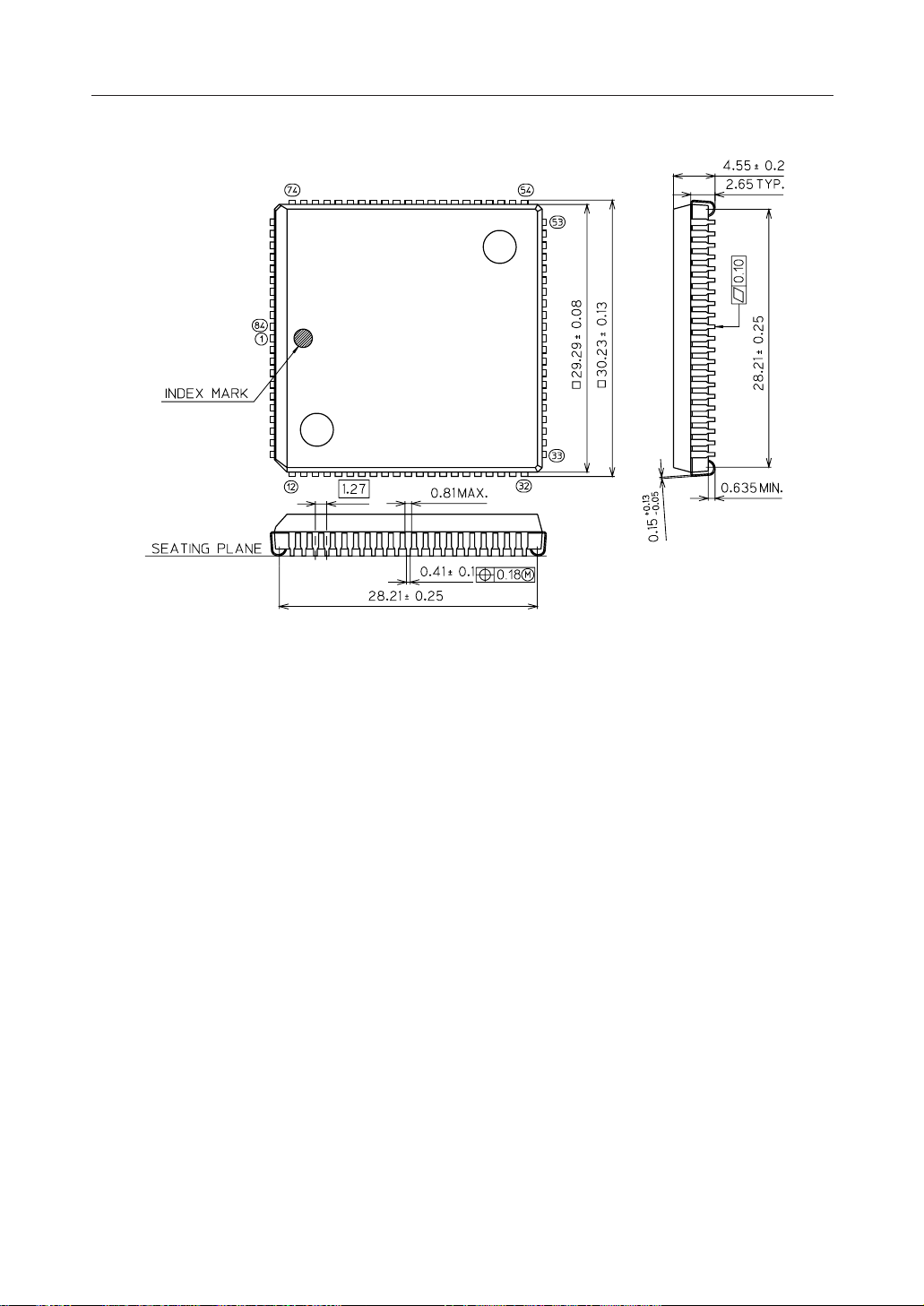
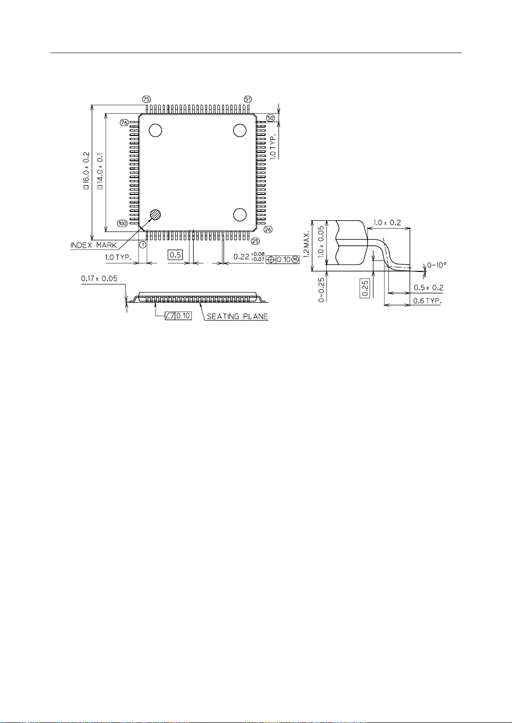
Figure 4. MSM6679A-110 84-Pin Package Mechanical Drawing
5
Page 8
MSM6679A-110 Voice Recognition Processor ¡ Semiconductor
N/C
VREF
N/C+
N/C+
N/C
N/C
N/C
N/C
RXD1
TXD1
N/C
GND
OSC0
N/C
OSC1
ALE
ROMRD
WRRAM
RDRAM
N/C–
RESOUT
NAR
N/C
N/C
DD
V
N/C
AVDDN/C
ADC0
ADC1
ADC2
ADC3
ADC4
ADC5
ADC6
ADC7
ADC8
ADC9
AGND
N/C
85
86
87
88
89
90
91
92
93
94
95
96
97
98
99
100
1
2
3
4
5
6
7
8
9
10
11
12
13
14
15
16
17
18
19
20
21
22
ES
23
24
25
N/C+
RES
EA
82
83
84
N/C
81
N/C
80
N/C
79
N/C
78
N/C
77
N/C
76
75
N/C
74
N/C
73
N/C
72
N/C
71
N/C
70
N/C
69
N/C
RAMPAGE1
68
67
RAMPAGE0
66
LOADPGM
65
N/C
64
N/C
GND
63
SD
62
SI
61
BUSY
60
59
N/C
N/C
58
ROMPAGE1
57
ROMPAGE0
56
STROBE
55
A15FLIP
54
53
N/C
N/C
52
N/C
51
50
49
48
47
46
45
44
43
42
41
40
39
38
37
36
35
34
33
32
31
30
29
28
27
26
N/C
VOICEOUT1
AD0
AD1
AD2
AD3
AD4
AD5
AD6
AD7
N/C
DD
V
N/C
A9
A8
A10
A11
A12
A13
A14
A15
N/C–
N/C
N/C
N/C
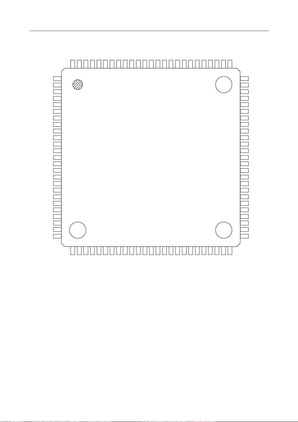
Figure 5. MSM6679A-110 100-Pin TQFP Pinout
6
Page 9
¡ Semiconductor MSM6679A-110 Voice Recognition Processor
Figure 6. MSM6679A-110 100-Pin Package Mechanical Drawing
7
Page 10

MSM6679A-110 Voice Recognition Processor ¡ Semiconductor
PIN DESCRIPTIONS
Pin #
84-pin/
100-pin
10/98 ADC9
11/99 AGND Analog ground
20/10 TXD1 Output Serial Port Transmit. This is the transmit data line for serial port.
21/12 GND Ground Ground.
22/13 OSC0 Input
23/15 OSC1 Output
24/16 ALE Output
Pin Name
-/1
1/89 ADC0
2/90 ADC1
3/91 ADC2
4/92 ADC3
5/93 ADC4
6/94 ADC5
7/95 ADC6
8/96 ADC7
9/97 ADC8
12/2 VREF
13/3 N/C+
14/4 N/C+
15/5 N/C
16/6 N/C
17/7 N/C
18/8 N/C
19/9 RXD1 Input Serial Port Receive. This is the receive data line for serial port.
-/11 N/C (not connected) Reserved. This pin is reserved for future use and should be left open.
-/14 N/C (not connected) Reserved. This pin is reserved for future use and should be left open.
N/C
Signal Type Description
(not connected) Reserved. This pin is reserved for future use and should be left open.
Analog Input. These ten inputs are tied together and serve as the
Analog input
Reference voltage
Input
(do not connected) Reserved. These pins are reserved for future use and must be left open.
analog input. Signal conditioning, via a bandpass filter and gain circuit,
is required before this input.
Analog Ground. This pin provides an analog ground point, allowing
independent grounding of the analog and digital circuitry. Separate
grounds reduce the impact of digital switching noise on analog
sampling accuracy.
Analog Reference Voltage. The MSM6679A-110's on-chip A/D
converter uses this analog reference voltage when converting an
analog signal into digital samples
Reserved. These pins are reserved for future use and must be tied to
VDD.
Oscillator 0/External Clock. When the MSM6679A-110 uses a crystal
oscillator, this input is the oscillator input pin. The pin is then
connected to one side of a crystal and load capacitor. When used with
an external clock, the external clock is applied to this input.
Oscillator 1. When the MSM6679A-110 uses a crystal oscillator, this
output is the oscillator output pin. The pin is then connected to one
side of a crystal and load capacitor. When used with an external clock,
this output is left unconnected.
Memory Address Latch Enable. An external memory latch is controlled
by this signal, the address latch enable output.
8
Page 11

¡ Semiconductor MSM6679A-110 Voice Recognition Processor
Pin #
84-pin/
100-pin
25/17
26/18 WRRAM Output
27/19 RDRAM Output
28/20 N/C– Input Reserved. This pin is reserved for future use and must be tied to GND.
29/21 RESOUT Output
30/22 ES Output
31/23 NAR Input
32/24 N/C (do not connect)
-/25,26 N/C (not connected)
33/27 VOICEOUT1 Output
34/28 AD0
35/29 AD1
36/30 AD2
37/31 AD3
38/32 AD4
39/33 AD5
40/34 AD6
41/35 AD7
42/37 VDD Digital Power Power.
43/39 A8
44/40 A9
45/41 A10
46/42 A11
47/43 A12
48/44 A13
Pin Name
ROMRD
-/36 N/C (not connected) Reserved. This pin is reserved for future use and should be left open.
-/38 N/C (not connected) Reserved. This pin is reserved for future use and should be left open.
Signal Type Description
ROM Read. This is a strobe signal for direct connection to an external
Output
Bidirectional I/O
Outputs Memory Address Bus. These are the upper eight address pins.
ROM's READ input. When asserted LOW, this signal indicates that the
MSM6679A-110 is ready to read data from the ROM.
RAM Write. This is a strobe signal for direct connection to an external
RAM's WR input. When asserted LOW, this signal indicates that the
MSM6679A-110 is ready to write data to RAM.
RAM Read. This is a strobe signal for direct connection to an external
RAM's RD input. When asserted LOW, this signal indicates that the
MSM6679A-110 is ready to read data from RAM.
MSM665x Reset. This pin provides a reset signal for an external
speech synthesis engine.
Flash Bank Control (Extended Segments). This is the control signal for
flash memory banking.
MSM665x Next Address Request. This pin signals to the
MSM6679A-110 that the external speech synthesis engine is ready for
another command.
Reserved. These pins are reserved for future use and must be left open.
Reserved. These pins are reserved for future use and should be left open.
Voice Out. This pin is the PWM output for speech synthesis, voice
sample playback, and voice prompts. An external integrator must be
used to convert this to an analog signal.
Memory Address/Data Bus. These are multiplexed address/data lines
for the eight data bits and the lower eight address bits (the upper eight
address bits are not multiplexed).
9
Page 12

MSM6679A-110 Voice Recognition Processor ¡ Semiconductor
Pin #
84-pin/
100-pin
49/45
50/46 A15
51/47 N/C– Input Reserved. This pin is reserved for future use and must be tied to GND.
52/48 N/C
53/49 N/C
-/50,51 N/C (not connected)
54/52 N/C
55/53 N/C
56/54 A15FLIP Output
57/55 STROBE Output
58/56 ROMPAGE0
59/57 ROMPAGE1
60/58 N/C (do not connect) Reserved. This pin is reserved for future use and must be left open.
61/60 BUSY Input
62/61 SI Output
63/62 SD Output
64/63 GND Digital Ground Ground.
65/65 N/C (do not connect) Reserved. This pin is reserved for future use and must be left open.
66/66 LOADPGM Output
67/67 RAMPAGE0
68/68 RAMPAGE1
69/69 N/C
70/70 N/C
71/71 N/C (do not connect)
72/72 N/C
73/73 N/C
74/74 N/C
-/75,76 N/C (not connected)
Pin Name
A14
-/59 N/C (not connected) Reserved. This pin is reserved for future use and should be left open.
-/64 N/C (not connected) Reserved. This pin is reserved for future use and should be left open.
Signal Type Description
Outputs Memory Address Bus. These are the upper eight address pins.
(do not connect)
(do not connect)
Outputs
Output
Reserved. These pins are reserved for future use and must be left open.
Reserved. These pins are reserved for future use and should be left open.
Reserved. These pins are reserved for future use and must be left open.
Memory Address A15 Flip. This signal inverts the A15 address signal
for 32-Kbyte bank switching on the local memory bus.
MSM665x Strobe. This output provides the LOAD signal for an external
speech synthesizer.
ROM Page Select. These signals select one of four 64-Kbyte ROM
pages.
MSM665x Busy. When using an external MSM665x device, this pin
monitors the MSM665x BUSY signal and connects directly to the
MSM665x BUSY signal output.
MSM665x Serial Clock. This MSM6679A-110 output connects to the
MSM665x SI input. The SI pin is the MSM665x serial clock input pin.
MSM665x Serial Data. This MSM6679A-110 output connects to the
MSM665x SD input. The SD pin is the MSM665x serial data input pin.
Load Program. This signal allows the MSM6679A-110 to write data to
program memory. When asserted low, this signal should set the
program memory in write mode.
RAM Page Select. These signals support selection of one out of four
RAM pages. Each page is 64kbytes in size.
Reserved. These pins are reserved for future use and must be left open.
Reserved. These pins are reserved for future use and should be left open.
10
Page 13
¡ Semiconductor MSM6679A-110 Voice Recognition Processor
Pin #
84-pin/
100-pin
75/77
76/78 N/C
77/79 N/C (do not connect)
78/80 N/C
79/81 N/C
80/82 N/C+ Input Reserved. This pin is reserved for future use and must be tied to VDD.
81/83 RES Input
82/84 EA Input
83/85 VDD
84/87 AVDD
-/100 N/C (not connected) Reserved. This pin is reserved for future use and should be left open.
Pin Name
N/C
-/86 N/C (not connected) Reserved. This pin is reserved for future use and should be left open.
-/88 N/C (not connected) Reserved. This pin is reserved for future use and should be left open.
Signal Type Description
Reserved. These pins are reserved for future use and must be left open.
MSM6679A-110 Reset. External logic should assert this power-on
reset signal LOW when power is applied to the MSM6679A-110.
External ROM Address Select. This control signal enables external
ROM execution. This signal is usually connected to ROMPAGE1 and a
pullup resistor.
Positive digital supply
Analog power supply
Power.
Analog Power.
11
Page 14
MSM6679A-110 Voice Recognition Processor ¡ Semiconductor
ELECTRICAL SPECIFICATIONS
Absolute Maximum Ratings
Digital power supply voltage
Input voltage
Output voltage
Analog power voltage
Analog reference voltage
Analog input voltage
Power dissipation
Storage temperature
Symbol Conditions
V
DD
V
I
V
AV
V
O
DD
REF
GND = AGND = 0 V
VAI –0.3 to V
PD
T
STG
Ta = 85˚C, per package 1300 max.
Ta = 85˚C, per pin 50 max.
— –50 to +150˚C ˚C
ValueParameter
–0.3 to +7.0
–0.3 to VDD +0.3
–0.3 to V
DD
+0.3
–0.3 to VDD +0.3
–0.3 to AVDD +0.3
REF
Unit
V
mW
1. Permanent device damage may occur if ABSOLUTE MAXIMUM RATINGS are exceeded.
Functional operation should be restricted to the conditions as detailed elsewhere in this
data sheet. Exposure to absolute maximum rating conditions for extended periods may
affect device reliability.
Operating Conditions
Digital power supply voltage
Analog power supply voltage
Analog reference voltage
Analog input voltage
Storage holding voltage
Operating frequency
Ambient temperature
Fan-out
Symbol
V
DD
AV
DD
V
REF
V
AI
V
DDH
f
OSC
Ta — –40 to 85˚C ˚C
N TTL load, AD0 ~ AD7 2
Conditions
f
= 32 MHz
OSC
VDD = AV
DD
ValueParameter
4.5 to 5.5
4.5 to 5.5
AVDD –0.3 to AV
A
to V
GND
REF
f
= 0 MHz 2.0 to 5.5
OSC
VDD = 5 V ±10% 32 MHz
MOS load 20
TTL Load, all other outputs 1
DD
Unit
V
12
Page 15
¡ Semiconductor MSM6679A-110 Voice Recognition Processor
DC Characteristics (VDD = 4.5 to 5.5 V, Ta = -40 to 85˚C)
Parameter Symbol Condition
High-level input voltage V
Low-level input voltage V
IH
IL
Output current = 400 mA, applied
High-level output voltage V
to AD0-AD7, ALE, and ROMRD
OH
Output current = 200 mA, for all
other I/O
Output current = 3.2 mA, applied
Low-level output voltage V
to AD0-AD7, ALE, and ROMRD
OL
Output current = 1.6 mA, for all
other I/O
= VDD/0 V, applied to Ain, EA,
V
Input leak current
I
IH
Input current
High-level output current I
Low-level output current I
Output leakage current I
Input capacitance C
Output capacitance C
Analog reference power
supply voltage
I
Power consumption I
I
FLOAT, and RESTART
, I
IL
= VDD/0 V, applied to RES
I
OH
OL
LO
I
f = 1 MHz, Ta = 25˚C
O
REF
DD
= 32 MHz, no load
OSC
Rated Value
Min Typ
[1]
2.2 V
0.85 × V
DD
0.80 × V
DD
–0.3 0.8—Applied to AD0-AD7
–0.3
–0.3 0.2 × V
—Applied to OSC0
—Applied to all other I/O
VDD –0.4 V——
VDD –0.4 ——
— 0.4—
— 0.4—
—
— 1/–250—V
— 15/–15—VI = VDD/0 V, applied to OSC0
–2 ——VO = 2.4 V, applied to AD0-AD7
–1
10 ——VO = 2.4 V, applied to AD0-AD7
5——VO = 2.4 V, applied to all other I/O
—
——7
—mA4—During voice input
— µA10—When voice input is halted
—mA7555f
Max
+0.3—Applied to AD0-AD7
DD
VDD +0.3—Applied to OSC0
VDD +0.3—Applied to all other I/O
0.15 × V
1/–1—
——VO = 2.4 V, applied to all other I/O
—5
Unit
DD
DD
µA
mA
µA±2—VO = VDD/0 V
pF
1. Typical condition is 5 V 25˚C.
13
Page 16

MSM6679A-110 Voice Recognition Processor ¡ Semiconductor
AC Characteristics
External Program Memory Control (VDD = 4.5 to 5.5 V, Ta = -40 to 85˚C)
Parameter Symbol Condition Min. Max. Unit
Clock pulse width (OSC) t
ALE pulse width t
ROMRD pulse width t
ROMRD pulse delay time t
Low address set-up time t
Low address hold time t
High address delay time t
High address hold time t
Instruction set-up time t
Instruction hold time t
OW
AW
PW
PAD
AAS
AAH
AAD
APH
IS
IH
15.625 ——
36.875 —
177.5 —
10.625 20.625
21.25ns41.25
10.625 20.625CL = 50 pF
15.625 25.625
15.625 25.625
35 —
0 25.625
External Data Memory Control (VDD = 4.5 ~ 5.5 V, Ta = -40 ~ 85˚C)
Parameter Symbol Condition Min. Max. Unit
Clock pulse width (OSC) t
ALE pulse width t
RDRAM pulse width t
WRRAM pulse width t
RDRAM pulse delay time t
WRRAM pulse delay time t
Low address set-up time t
Low address hold time t
High address set-up time t
High address hold time
Memory data set-up time t
Memory data hold time t
Data set-up time t
Data hold time t
WAD
t
ARH
t
AWH
OW
AW
RW
WW
RAD
AAS
AAH
AAD
MS
MH
DD
DH
C
= 50 pF
L
,
15.625 ——
36.875 —
177.5 —
177.5 —
10.625 20.625
10.625 20.625
21.25 41.25
10.625 ns20.625
15.625 25.625
15.625 25.625
35 —
0 5.625
15.625 25.625
15.625 25.625
14
Page 17

¡ Semiconductor MSM6679A-110 Voice Recognition Processor
Timing Diagrams
tOWt
OW
CLK
t
AW
ALE
ROMRD
AD0 - AD7
A8 - A15
CLK
ALE
tOWt
t
PAD
t
AAS
t
AAH
PC0 - 7
t
AAD
PC8 - 15
Figure 7. ROM Read Timing
OW
t
AW
t
PW
t
IS
t
IH
INST0 - 7
t
APH
RDRAM
AD0 - AD7
A8 - A15
t
RAD
t
AAS
t
AAH
RAP0 - 7
t
AAD
RAP8 - 15
Figure 8. RAM Read Timing
t
RW
t
MS
t
MH
INST0 - 7
t
ARH
15
Page 18

MSM6679A-110 Voice Recognition Processor ¡ Semiconductor
tOWt
OW
CLK
t
AW
ALE
WRRAM
AD0 - AD7
A8 - A15
t
WAD
t
DD
t
AAS
t
AAH
RAP0 - 7
t
AAD
RAP8 - 15
Figure 9. RAM Write Timing
t
WW
DOUT0 - 7
t
t
DH
AWH
16
Page 19

¡ Semiconductor MSM6679A-110 Voice Recognition Processor
FUNCTIONAL DESCRIPTION
Voice Recognition
The MSM6679A-110 performs both SD and SD recognition. SI vocabularies are embedded in the
MSM6679A-110. For SD recognition, each recognized phrase must be enrolled in the MSM6679A110’s vocabulary by creating a composite template from multiple recordings of the same phrase.
Then the com-posite tempalte is stored in SRAM or FLASH memory. During both SI and SD
recognition, the MSM6679A-110 performs the following steps:
1. After external band-pass filtering, the MSM6679A-110 converts the analog signal to PCM
samples.
2. The MSM6679A-110 extracts significant features from the sample data by frequency and
time-domain analysis.
3. The MSM6679A-110 compares the analyzed input with the reference data for each signal,
weighing the significance of similarities according to control software parameters. A score
(expressed as distance) is generated for each phrase.
4. he vocabulary phrase that achieves the highest score (or lowest distance) is judged to match
the input phrase, assuming that the score exceeds a predetermined threshold.
5. Via a special command, the MSM6679A-110 can also return the scores of the input against all
defined vocabulary phrases for SI or SD recognition. This feature allows external host
software to select the next best match, if the closest match is not contextually logical.
SI Recognition
Oki supplies the MSM6679A-110 with predefined SI vocabularies which Oki builds from
hundreds of utterances by a wide variety of speakers. SI vocabularies are limited to 25 words or
less, which allows the MSM6679A-110 to achieve a net accuracy of >95%, even in noisy
conditions.
SI vocabularies are grouped into sub-vocabularies of ≤15 words, to maintain the highest
accuracy. Similar words in any one sub-vocabulary can cause substitution errors.
Oki Semiconductor’s standard cellular vocabulary is intended for an automotive environment
with a far-talk microphone. This vocabulary may work adequately in other conditions, such as
an office or outside, but recognition performance may be degraded.
MSM6679A-110 Cellular SI Recognition Vocabulary
Sub-Vocabulary 1 Sub-Vocabulary 2 Sub-Vocabulary 3
Phrase
Store
Dial 2 Two 2
Delete 3 Three 3
Directory 4 Four 4
— — Five 5
— — Six 6
— — Seven 7 — — — —
Index Phrase Index Phrase Index Phrase Index
1 One 1 Yes 1
Eight 8
Nine 9
Zero Ah
Oh Bh
Stop Ch
Clear Dh
No 2
Cancel 3
——
——
——
17
Page 20

MSM6679A-110 Voice Recognition Processor ¡ Semiconductor
MSM6679A-110 Control Vocabulary
Sub-Vocabulary 1 Sub-Vocabulary 2
Phrase
A/C
Fan 2 Medium 2
Temperature 3 High 3
Timer 4 Increase 4
Service 5 Decresse 5
Help 6 Set 6
Select 7 Reset 7
— — Cancel 8
— — Clear 9
— — Recall A
— — On B
— — Help C
Index Phrase Index
1 Low 1
MSM6679A-110 Direction Vocabulary
Sub-Vocabulary 1
Phrase
Up
Down 2
Left 3
Right 4
Formard 5
Reverse 6
Faster 7
Slower 8
Start 9
Stop A
Cancel B
Index
1
MSM6679A-110 Browse Vocabulary
Sub-Vocabulary 1 Sub-Vocabulary 2
Phrase
Up
Down 2 Previous 6 — — Reset 2 Play 6
Left 3 Select 7 — — Start 3 Lock 7
Right 4 Cancel 8 — — Stop 4 Cancel 8
Index Phrase Index Phrase Index Phrase Index Phrase Index
1 Next 5 Home 9 Set 1 On 5
18
Page 21

¡ Semiconductor MSM6679A-110 Voice Recognition Processor
MSM6679A-110 Japanese Navigation Vocabulary
Sub-Vocabulary 1 Sub-Vocabulary 2 Sub-Vocabulary 3 Sub-Vocabulary 4
Phrase
Genzaichi
Jiaku 2 Shita 2 Kakudai 2 Iie 2
Kaisya 3 Hidari 3 Shukushou 3 Ofu 3
Houi 4 Migi 4 Zentai 4 — —
Sentaku 5 — — Kaiten 5 — —
Yuudou 6 — — Kyori 6 — —
Nabi 7 — — Hosei 7 — —
— — — — Teisei 8 — —
Index Phrase Index Phrase Index Phrase Index
1 Ue 1 Hyoujun 1 Hai 1
MSM6679A-110 Japanese Celluar Vocabulary
Sub-Vocabulary 1 Sub-Vocabulary 2
Phrase
On
Ofu 2 Ni 2 Zero A
Daiyaru 3 San 3 Sharp B
Tansyuku 4 Yon 4 Star C
Denwacho 5 Go 5 Kakunin D
Kakunin 6 Roku 6 Touroku E
Nabi 7 Nana 7 Rei F
— — Hachi 8 — —
Index Phrase Index Phrase Index
1 Ichi 1 Kyuu 9
SI vocabulary generation starts with collecting reference utterances from ≥400 speakers with:
• An equal mixture of males and females
• Accents from all regions of the country of intended use
• ~15% non-native speakers.
The samples should be generated from a randomly-ordered list, with each word spoken twice
and with a dummy word at the beginning and end. There must be >2 sec between each sample
for accurate data processing. To provide the audio fidelity required for high-quality recognition
training, a DAT recorder, together with the microphone that will be used in the final application,
is required. To ensure data integ-rity, data is submitted to Oki after collecting samples from the
first 20 speakers for initial screening. If acceptable, then the remaining collection may proceed.
If substitution errors are possible, collection of spare words during initial collection is
recommended. For example, alternate words to “Stop” and “Top” could be “Halt” and “First.”
Collections should contain a wide variety of the background sound conditions that will exist
during actual usage. For example, if the collection is for use in an automobile, conditions such
as vehicle speed, road conditions, various window opening positions, heater or AC blower
speeds and radio volumes should be varied during the collection. The signal-to-noise ratio
should be maintained at ≥ 20dB.
19
Page 22

MSM6679A-110 Voice Recognition Processor ¡ Semiconductor
To achieve high accuracy rates, phrase selection, data collection, background initialization
strategy, and control software need careful consideration. There are no published standards for
recognition accuracy.
Oki defines accuracy by:
Accuracy = 100% - E
E
RATE
= E
SUB
+ 1/2 E
RATE
REJ
with the following definitions:
Parameters for Recognition Accuracy
Name ConditionSymbol
Substitution Error Most critical type error, e.g., Say "Five", recogrize "Nine"E
Rejection Error Word not recognized, opportunity for operator to repeatE
Gap Error Word spoken before recognizer readyE
Time-Out Error Word length is too longE
Spurious Response Error
E
SUB
REJ
GAP
TME
Sourd or imvalid word classfied as a valid word
SPU
(i.e., drop handset or speak wong word)
A typical target accuracy of 97% is achieved with a 3% E
a 3%E
REJ
rate.
, composed of a 1.5% E
RATE
rate and
SUB
SD Recognition
In SD recognition mode, the MSM6679A-110 can be trained to recognize up to 61 words. The
MSM6679A-110 can support multiple speakers by switching vocabularies, but only one speaker’s
vocabulary should be active at one time.
The end user enrolls a phrase in the MSM6679A-110’s vocabulary by recording the phrase three
times or more. The host Micro Controller Unit (MCU) controls the number of times each phrase
in enrolled. Generally, higher recognition accuracy is achieved with each additional enrollment.
The word set is made more robust by pronouncing each phrase slightly differently during initial
enrollment.
In addition to enrollment training, adaptive template updating can drive the accuracy towards
100%. The host MCU updates templates by first asking the speaker to confirm a recognized
phrase with a “yes” or “no” response, and subsequently updating the template for corresponding
words. The use of name tags (see next paragraph) facilitates this process.
Name Tag Recording
To facilitate SD recognition, the MSM6679A-110 supports recording and playback of name tags.
Name tags are used to confirm correct responses in SD recognition. For example, in a phone
dialer application, the user associates a “name” (which is recorded into memory) with a phone
number. The MSM6679A-110 then plays back the name tag so that the user can verify that the
recognized phrase is the correct one.
The VRP stores names tags in memory using an ADPCM compression algorithm with 28 kbps
of speech. The length of a name tag is controlled with a command from the users host MCU
program. The maximum number of name tags possible is 61, but the actual number is dependent
upon record time and memory available. See the section on memory interface for more detail.
20
Page 23

¡ Semiconductor MSM6679A-110 Voice Recognition Processor
Audio Input Interface
A critical item for high-accuracy speech recognition is correct design of the audio input circuit.
A circuit with appropriate gain and frequency responses must be placed between the microphone
and MSM6679A-110’s A/D input. Oki recommends input gain and a band pass filter with the
following characteristics:
• Four pole Chebyshev high-pass filter, 3 dB point at 225 Hz
• Dual-pole low-pass filter, 3 dB point at 4250 Hz
• Midband gain of 46 dB at 1000 Hz
The above gain and filter characteristics are obtained by using a rail-to-rail quad CMOS op-amp
and one-half supply rail splitter to bias the input signal at 2.5 V nominal.
The MSM6679A-110 uses multiple analog inputs to improve sampling quality. An on-chip
analogy to digital (A/D) conversion unit transforms the analog signal to a digital data stream.
Audio Output Interface
The MSM6679A-110 also provides the VOICEOUT1 PWM output. The MSM6679A-110 uses
ADPCM to generate voice or sound-effect output. ADPCM represents an improvement over
conventional PCM techniques in that it adaptively changes the quantizer step (scale factor) to suit
the waveform being encoded. The result is more efficient memory usage with no loss of quality.
Careful selection of the components for internal and external output filters and amplifiers is
recommended. An incorrect choice would impair the original quality. This consideration equally
includes:
• Careful separation of analog and digital lines
• Grounding of analog lines at both ends
• Further adequate separation from high-speed digital circuits to avoid distortions thereof
Memory Interface
The memory control section manages RAM and/or ROM devices in two 64-Kbyte memory
spaces, in conjunction with internal memory for voice templates and working memory. Some
versions work with no external memory, some have some external RAM, some use only external
EPROM, and some use external memory in conjunction with both internal ROM and RAM. The
MSM6679A-110 requires a minimum of 32 Kbytes SRAM and 16 Kbytes ROM.
The following table shows vocabulary sizes and playback facilities for various configurations.
21
Page 24

MSM6679A-110 Voice Recognition Processor ¡ Semiconductor
Typical Configurations
MSM6679A-110
Sound Playback
(sec)
Internal
[2]
2.3 9.2 OK — OKController
[2]
2.3 — OK — OK
61 2.3 36.8 OK — OK — —
[2]
1.15 OK — — 16K — 32K
MSM665x
MSM6679A-110
Playback
[1]
External EPROM
Interface
Speech
Record
MSM6679A-110
Speech
Playback
Memory Size
64K — 32K
— 128K 32K
(bytes)
Flash SRAM
64-384K
Application
Telephone
Dialer
Computer
Peripheral
Minimum
Configuration
Recognition
Vocabulary
(Words)
SI SD
25 61
50 61
25 61 2.3 27.6 OK OK OK
50 61 2.3 18.4 OK OK OK
75 61 2.3 — OK OK OK
100 61 2.3 — OK OK OK
[3]
61
12 61
1. Phrase chaining features usually permit much longer overall playback durations; not
including external speech synthesizer.
2. SD recognition vocabularies are volatile in these configurations.
3. Per download. Vocabulary swapping by host permits unlimited vocabulary size.
The MSM6679A-110 supports up to 64 Kbytes of RAM per bank, and up to 64 Kbytes of ROM per
bank in separate memory spaces. The 8-bit data bus is multiplexed with the lower eight address
bits; the upper eight address bits are not multiplexed.
To demultiplex the address and data bits during all read and write cycles, the MSM6679A-110
requires an external octal latch, such as the 74H373. The MSM6679A-110’s Address Latch Enable
(ALE) signal controls the octal latch.
For accessing the ROM and RAM address spaces, the MSM6679A-110 provides the separate
Write RAM (WRRAM), Read RAM (RDRAM), and ROM Read (ROMRD) signals. The RDRAM
and ROMRD signals connect directly to Output Enable (OE) control signal inputs on the RAM
and ROM, respectively. The WRRAM signal connects directly to the Write Enable (WE) control
signal input on the RAM.
The following diagrams show the memory maps for the MSM6679A-110. In all MSM6679A-110
memory maps, the DL data memory space must be in RAM. The DH data memory space and PH
program memory space can either be implemented in ROM, EPROM, FLASH, RAM, or PROM.
In standalone applications, flash memory can be used for recording and subsequent playback of
voice prompts (e.g., the user’s name) and user sounds (e.g., DTMF dial tones, etc.).
Figure 10 shows the configuration for writing to flash memory used when writing SD templates
or when flash is used for data memory.
22
Page 25

¡ Semiconductor MSM6679A-110 Voice Recognition Processor
FLASHProgram Memory Data Memory
00000
BFFF
C000
FFFF
MSM6679
Internal
Program
Memory
PHH
00000
03FFF
04000
07FFF
08000
08FFF
0C000
0FFFF
10000
13FFF
14000
17FFF
18000
18FFF
1C000
1FFFF
F0
F1
F2
F3
F4
F5
F6
F7
00000
DL
07FFF
08000
DH
0FFFF
Figure 10. MSM6679A-110 Program/Data Memory Map (LOADPGM = “0”)
Figure 11 shows the memory map during all other modes of operation.
FLASHProgram Memory Data Memory
00000
BFFF
C000
FFFF
MSM6679
Internal
Program
Memory
PHH
00000
03FFF
04000
07FFF
08000
08FFF
0C000
0FFFF
10000
13FFF
14000
17FFF
18000
18FFF
1C000
1FFFF
F0
00000
DL
F1
F2
07FFF
08000
DH
F3 S3
0FFFF
F4
F5
F6
F7
00000
07FFF
08000
0FFFF
10000
17FFF
18000
1FFFF
00000
07FFF
08000
0FFFF
10000
17FFF
18000
1FFFF
SRAM
SO
S1
S2 Hidden
S3
SRAM
S0
S1
S2
Figure 11. MSM6679A-110 Program/Data Memory Map (LOADPGM = “1”)
Figure 12 shows the details of the external memory allocation of the MSM6679A-110.
23
Page 26

MSM6679A-110 Voice Recognition Processor ¡ Semiconductor
FLASH
00000
SI First (F509*)
07300
SD First
07D80
NTP First
Name Tag Block Address
08000
10000
Name Tag Data
18000
SI Last
(F501*)
1F900
SD Last
1FD80
NTP Last
1FFFF
*Denotes commands to select blocks
000
100
200
2F6
2FB
2FF
FLASH
Reserved
04AD0
Default Working SD
Templates
05480
Working Name Tag
Pointer Table
05700
Alternate SD Templates
08000
Down load RAM Bank
0F300
10000
(F510*)
Alternate SD Templates
Reserved
18000
Buffer RAM Bank (F520*)
1F300
Reserved
1FFFF
Figure 12. MSM6679A-110 External Memory Map
External Voice Synthesis Control
The MSM6679A-110 is capable of interfacing to the MSM665x family of Oki ROM, OTP, or
external EPROM speech synthesizers, allowing for up to 260 seconds of high-quality voice and
sound effects. The following table indicates the speech capabilities of the MSM665x family.
MSM665x Family Characteristics
f
= 16.0 kHz f
SAM
[2]
= 32.0 kHz
SAM
>8 minutes
Type
MSM6650
Data ROM
Capacity
64 Mbits
[3]
[1]
f
= 4.0 kHz f
SAM
SAM
>1 hour >40 minutes
Maximum Speech Duration
= 6.4 kHz f
= 8.0 kHz
SAM
>30 minutes >15 minutes
MSM6652 288 Kbit 16.9 sec 10.5 sec 8.4 sec 4.2 sec 2.1 sec
MSM6653 544 Kbit 31.2 sec 19.5 sec 15.6 sec 7.8 sec 3.9 sec
MSM66P54
[4]
1 Mbit 63.8 sec 39.9 sec 31.9 sec 15.9 sec 7.9 sec
MSM6654 1 Mbit 63.8 sec 39.9 sec 31.9 sec 15.9 sec 7.9 sec
MSM6655 1.5 Mbit 96.5 sec 60.3 sec 48.2 sec 24.1 sec 12.0 sec
MSM66P56
[5]
2 Mbit 129.1 sec 80.7 sec 64.5 sec 32.2 sec 16.1 sec
MSM6656 2 Mbit 129.1 sec 80.7 sec 64.5 sec 32.2 sec 16.1 sec
MSM6658 4 Mbit 258 sec 161.4 sec 129.1 sec 64.5 sec 32.2 sec
1. Actual ROM area in MSM6652, MSM6653, MSM6654, MSM6655, and MSM6656, MSM6658,
MSM66P54, MSM66P56 is smaller by 22 Kbits.
24
Page 27

¡ Semiconductor MSM6679A-110 Voice Recognition Processor
2. Longer speech patterns can be created by chaining and repeating existing speech samples.
3. Via external ROM only (no on-chip ROM available).
4. One-Time-Programmable (OTP) version of MSM6654. See the MSM66P54 data sheet for
more information.
5. One-Time-Programmable (OTP) version of MSM6656. See the MSM66P56 data sheet for
more information.
The MSM665x interface consists of the following signals:
• BUSY - Asserted LOW during MSM665x device playback. The MSM6679A-110 F50Bh and
F10100xxh commands select this signal for MSM665x command polling.
• NAR - Next Address Request status signal. By default, the MSM6679A-110 uses this signal to
poll commands to the MSM665x. The F51Bh, F480h, and F440h commands select NAR for
polling.
• SI - Serial Input Clock.
• SD - Serial Data Out.
• STROBE - Initiates speech synthesis.
• RESOUT - Initializes device when asserted LOW. The MSM6679A-110 F480h command
generates this signal.
Serial Interface
The MSM6679A-110 supplies a serial interface suitable for connection to an RS-232C serial port
buffer or equivalent. The serial interface uses one MSM6679A-110 input (RXD) and one
MSM6679A-110 output (TXD). The interface operates at 9600 Baud with:
• 8 data bits
• 1 start bit
• 1 stop bit
• No parity
• No handshake
A host processor sends serial ASCII commands to the MSM6679A-110 and receives serial ASCII
responses based on voice input responses.
25
Page 28

MSM6679A-110 Voice Recognition Processor ¡ Semiconductor
MSM6679A-110 SLAVE-MODE API
This section describes the slave-mode Applications Protocol Interface (API) between a host MCU
and the MSM6679A-110. The slave-mode API offers the following features:
• Direct slave-mode control voice recognition, sound recording and playback, and sound
synthesis
• Serial port interfaces
• Simple procedures for downloading and uploading data
• ASCII format
• Comprehensive return codes and error reporting
The host MCU selects the active speech recognition vocabulary, speech responses, and controls
all actions required to implement an interactive voice response system. The MSM6679A-110
performs speech recognition, based on the vocabulary selected by the host, and returns digital
codes representing the most probable match of the current utterance to an individual utterance
in the selected vocabulary. The MSM6679A-110 can also respond with “name tags.” Name tags
can be fixed words, phrases or sound effects, or can be words, phrases or sound effects that have
been interactively recorded by the user.
The API supports serial interface. The MSM6679A-110 returns each response using the same
interface through which the most recent message was received. The user can thus connect and
use both interfaces.
For all messages, the serial interface represents each 8-bit value with two hexadecimal digits
coded in ASCII. When downloading and uploading data, the MSM6679A-110 uses a stream of
8-bit binary values.
The serial-mode interface uses a 9600-baud UART with 1 start bit, 8 data bits, and 1 stop bit. There
is no parity or handshaking. Serial-interface messages are of variable length, but consist of an
even number of bytes. The serial interface echoes all received ASCII characters immediately back
to the host MCU.
Messages are of variable length. All messages consist of an even number of bytes. Opcodes
consist of exactly four bytes, with values between F000h and FEFEh. Operand bytes may take
values from 0000h to FFFFh. The MSM6679A-110 issues a return code for many of the host
commands. The return code generally consists of the same opcode, followed by data indicating
success of failure of the operation.
Opcodes are organized into the following categories:
• Purge
• Set parameter
• Initialize
• Recognize
• Speak
• Request
• Record
• SD recognition control
The following tables summarize available opcodes and provide detailed descriptions of the
opcode functions.
26
Page 29

¡ Semiconductor MSM6679A-110 Voice Recognition Processor
Command Summary
Function
Purge
Set parameter
Initialize
Recognize
Speak
Request
Opcode (Hex) Description
F000 Clear MSM6679A-110 input stack
F102 xxxx
F103 xxxx
F104 xxxx
F11x
F12x
F130 xxxx
F440
F2xx mod 80
F2xx mod 40
F2xx mod 20
F2xx mod 10
F2xx mod 8
F2xx mod 4
F2xx mod 2
F2xx mod 1
F300
F301 to F33F
F340
F341
F342
F343
F344
F351
F361
F371
F401 to F43D
F441 to F47C
F47E
F47F
F480
F481 - F4FF
F50B
F51B
FE03 to FEFE
F500
F501
F510
F520
F522
F513
Set SP/SI origin to xxxx.
Set SD origin.
Set triggering origin.
Set IRQ level to IRQ x.
Set SD SP table to table x.
Select triggering table.
Set ISA mode.
Initialize background estimation.
Wait for F3h command after each response.
Beep after each triggered utterance
Reserved
Set speech response level to default.
Send acknowledge after each speech output response.
Only detect triggers.
Initialize SD parameter table and name tags.
Stop listening (recognition).
Start SI recognition.
Start SD recognition.
Sort SD recognition distances, return index to utterance with
least distance.
Update SD enrollment.
Request recognition parameter upload to host.
Sort SD recognition distances, return index and distance to
utterance with least distance
Sort SD recognition distances, return all distances.
Sort SD recognition distances, return minimum and
maximum energy values.
Sort SD recognition distances, return all energy values and
distances.
Play back name tag from external memory.
Play back sound from internal memory.
Play 50-ms beep.
Pause for 0.2 sec.
Initialize MSM665x IC, set MSM665x busy mode OFF, select
FLASH SI recognition.
Play back one of 127 phrases in external MSM665x device.
Set MSM665x busy mode ON.
Set 6654 NAR mode
Set output volume (03h = minimum, FEh = maximum).
Status request.
Select last FLASH bank for SI recognition.
Select download RAM bank for speaker independent/signal
processing (SI/SP) template area.
Select buffer RAM bank for SI/SP.
Copy download RAM bank to buffer RAM bank
Save download RAM bank templates in first FLASH.
(8000 - F2FF)
Default (Hex)
—
8000
4A00
F100
0005
F123
0101, 0202...
Disabled.
Disabled.
Disabled.
Disabled.
Disabled.
Enabled.
Enabled.
Disabled.
Load from first
FLASH.
—
—
—
—
—
—
—
—
—
—
—
—
—
—
—
—
OFF
ON
FE80h
—
F509
F509
—
—
—
27
Page 30

MSM6679A-110 Voice Recognition Processor ¡ Semiconductor
Function
Request
Record
SD
Recognition
Control
Opcode (Hex) Description
F514
Get download RAM bank templates from the first FLASH
(8000 - FFFF)
F515
Save download RAM bank templates is last FLASH
(8000 - F2FF)
F516
Get download RAM bank templates from last FLASH
(8000 - FFFF)
F502....
F503 xxxx
F504
F505
F506
F507
F517
F508
F518
F509
F101 00xx
F105
F106
F50A
F50C
F51C
Download/upload.
Select/jump.
Retrieve MSM6679A-110 firmware revision.
Initialize background (BG) noise level.
Retrieve vocabulary and trigger table revision number.
Save SD templates from download RAM to first FLASH.
Save SDR templates in last FLASH. (4A00-547B→F300-FD7F)
Recall SD templates from first FLASH to download RAM.
Get SDR Templates from last FLASH (F300-FD7B→4A00-547B)
Select first FLASH bank for SI recognition.
Set name tag length, set MSM665x busy mode ON.
Set name tag record origin
Set name tag record end
Clear name tag table in SRAM (5480 - 56FF).
Recall last saved name tag table.
Recall name tag pointers from last FLASH
(FD80-FFFF→5480-56FF)
F50D
F51D
F50E
F50F
FA01 ~ FA3D
F6xx
F9xx
FB00
FC00
F521
Save name tag table from SRAM to FLASH.
Save name tag pointers in last FLASH (5480-56FF→FD80-FFFF)
Set record volume high.
Set record volume normal (default).
Record name tag 01h - 3Dh.
Set SD pointer to segment xxh.
Search for SD utterance xxh.
Enroll SD utterance selected by search command (F9xx).
Erase utterance from SD vocabulary.
Clear SDR table (4A00 - 547B)
Default (Hex)
—
—
—
—
—
3136
—
3330
—
—
—
—
F509
0051
0000
01FF
—
—
—
—
—
F50F
F50F
—
—
—
—
—
—
Response Summary
Command
F101h 00 tm
F102h AdH AdL
Result after
Parameter Set
F103h AdH AdL
F104h AdH AdL
F11Xh
F12Xh
F280h
F240h
F220h
Initialization
Acknowledgment
F210h
F208h
F204h
F202h
F201h
Speech Ack F400h Speech acknowledgment.
Operands Description
Record time = tm*14 msec.
High and low bytes of SP/SI origin address.
High and low bytes of SD origin address.
High and low bytes of triggering origin address.
IRQ Xh selected.
SP table Xh selected.
Invalid message received.
Sample data over-run.
32-Kbyte block boundary violation error.
Unclassified download/upload error.
Divide-by-zero error.
Select/jump error.
Invalid SP header or table.
Reserved.
28
[1]
[2]
Page 31

¡ Semiconductor MSM6679A-110 Voice Recognition Processor
Response Summary (Continued)
Command
[3]
Status
SI Recognition
[5]
Result
SD Recognition
Result
Vector Upload
Trap Error
Codes
Record Response
Operands Description
F500h
F501h
F520h
F540h
F560h
F580h
F5A0h
F5C0h
F5E0h
F5F0h
F600h
F6Utt
F6 Utt Dst1H Dst1L...DstNH DstNL
F6 Utt EminH EminL EmaxH EmaxL
F6 Utt Dst1H Dst1L...DstNH DstNL
EminH EminL EmaxH EmaxL
MSM6679A-110 ready.
Operation complete.
Operations complete; MSM6679A-110 disabled (vocabulary 0).
MSM6679A-110 waiting for start command.
MSM6679A-110 waiting for end trigger.
MSM6679A-110 processing recognition.
Download/upload in progress.
Download/upload complete.
Select/jump complete.
Speak output in progress.
Aborting SI listen mode.
Utt = utterance ID.
Utterance ID, high/low byte of distance to utterance 1...utterance N.
Utterance ID, high/low byte of min. and max. energy value,
Utterance ID, high/low byte of distance to utterance 1...utterance N,
high/low byte of minimum energy value, high/low byte of
maximum energy value.
F63Ah
F63Bh
F63Ch
F63Dh
F63Eh
F63Fh
F700h
F73Eh
F73Fh
F740h
Trigger detection code (see init command).
Rejection: utterance too loud.
Rejection: utterance too long.
Rejection: utterance begins too soon.
Rejection: bad signal/noise ratio.
Rejection: reason uncertain.
Aborting SD Listen mode. After SD utterance search: not found.
Rejection.
Sort completed. After SD utterance search: empty.
Rejection: MSM6679A-110 SD memory full/empty. After SD
utterance search: in use.
F341h F7Utt
F344h F7Utt DstH DstL
F351h F7Utt Dst1H Dst1L...
DstNH DstNL
F361h F7Utt EminH EminL
EmaxH EmaxL
F371h F7Utt Dst1H Dst1L...
DstNH DstNL
EminH EminL EmaxH EmaxL
F743h 0000h
F743h NH NL V1H V1L...VNH VNL
F801h
F802h
F804h
F808h
F810h
F820h
F840h
F880h
Utt = Utterance ID triggered.
Utterance ID, high/low byte of distance.
Utterance ID, high/low byte of distance to utterance 1...
utterance N.
Utterance ID, high/low byte of minimum energy value,
maximum energy value.
Utterance ID, high and low byte of distance to utterance 1...
distance to utterance N, high and low byte of minimum energy
value, maximum energy value.
Upload failure.
High/low bytes of length of vector, V, high/low byte of first V...Nth V.
Reserved.
Invalid SP header or table.
Select/jump error.
Divide-by-zero error.
Unclassified download/upload error.
Memory full; 32-Kbyte block boundary violation error.
Sample data over-run.
Invalid message received.
FA00 Record complete.
[4]
[1]
29
Page 32

MSM6679A-110 Voice Recognition Processor ¡ Semiconductor
1. Sample data overrun issued when real-time SP in Listen mode cannot keep up with
incoming samples, i.e., if the A/D signal input routine overwrites a sample data buffer
before it is fully processed.
2. This acknowledge is sent only if Init command 1111 0010 xxxx x1xx (F2 xxxx x1xx) is set
to enable acknowledgments.
3. These messages are sent in response to a request command (F5XYh) from the host.
4. Upload/download in progress, acknowledging load request immediately before data
transfer. If in response to an N-byte download request, the MSM6679A-110 then receives
N bytes (if N is even, or N+1 if N is odd) of data from the host. If N is odd and N+1 bytes
are received, only N bytes are written to MSM6679A-110 memory. If in response to an
upload, the MSM6679A-110 then sends N bytes (if N is even, or N+1 if N is odd) of data
to the host.
5. If an utterance was recognized, XYh is the utterance identity or class number, and
additional parameters may be appended, if requested in the SI Recog (F3XYh with X=0...3)
command. Otherwise, XYh indicates various results as detailed.
30
Page 33

¡ Semiconductor MSM6679A-110 Voice Recognition Processor
Command Descriptions
Purge
Operand
F000
Set Parameter
Operand
F102h XXYYh
F103h XXYYh
F104h XXYYh
Purge MSM6679A-110 Input Stack. This command clears the
MSM6679A-110 input stack of commands that are waiting to
be executed. Commands already in progress, such as a
pending MSM6654 poll action, are not affected. It does not
affect the MSM6679A-110 output stack.
Description
Set SP/SI Recognition Origin. Prior to SD or SI recognition,
address pointers must be set to point at the SP or SI
recognition parameter tables.This command sets the starting
address of SP and SI recognition parameter tables.
This address is the location of the first word of a header that
contains pointers to one or more individual SP/SI tables.
XXYYh = high (XXh) and low (YYh) bytes of requested
address. The MSM6679A-110 uses and returns an even
address outside the MSM6679A-110 work space that is as
near as possible to the requested address.
Leave this parameter at its default value unless you are using
an Oki custom SI vocabulary and are instructed to alter SP/SI
recognition origin.
Default SP/SI origin: 8000h
[2]
Set SD Recognition Origin
origin address at the starting address of the current SD
recognition parameter table. This command may be used to
select among mul-tiple RAM-resident SD vocabulary tables.
XXYYh = high (XXh) and low (YYh) bytes of requested
address. The MSM6679A-110 uses and returns an even
address outside the MSM6679A-110 work space that is as
near as possible to the requested address.
Leave this parameter at its default value unless you are using
an Oki custom vocabulary and are instructed to alter SD
recognition origin.
The table length is 0A7Ch bytes.
Set Triggering Origin. This command sets the starting
address of triggering parameter tables.
This address is the location of the first word of a section of
data memory containing one or more contiguous triggering
parameter tables.
XXYYh = high (XXh) and low (YYh) bytes of requested
address. The MSM6679A-110 uses and returns an even
address outside the MSM6679A-110 work space that is as
near as possible to the requested address.
Leave this parameter at its default value unless you are using
an Oki custom SI vocabulary and are instructed to alter
triggering origin.
. This command sets the SD
Default SD origin: 4A00h
Default triggering origin: F100h.
Return ValuesDescription
None
Return Values
F102h XXYYh = High (XXh) and
low (YYh) bytes of resultant
address.
If a valid header is not found at
the resultant address, the
MSM6679A-110 immediately
sends response code:
F802h = Invalid SP/SI header.
F103h XXYYh = high (XXh) and
low (YYh) of resultant address.
F104h XXYYh = high (XXh) and
low (YYh) bytes of resultant
address.
[1]
31
Page 34

MSM6679A-110 Voice Recognition Processor ¡ Semiconductor
Set Parameter (Continued)
Operand
Set IRQ Level. This command requests direction of host
interrupts to IRQ Y. The MSM6679A-110 then selects IRQ Z,
F11Yh
F12Yh
F130h VN TN
F440h None. Default is off.
where Z is the nearest legal value to Y. Legal IRQ values are
any from the set {5 (default),A,B,C}.
Set SD Recognition SP table. This command sets the SP
parameter table number to be used in processing speech
input during SD Recognition. The MSM6679A-110 selects SP
table number Z, where Z is the nearest valid value to Y. By
default, the MSM6679A-110 selects SP table 3 until this
command is issued. This command selects SP parameters
only, and does not select among multiple RAM-resident SD
vocabulary tables, which can be independently selected by the
Set SD Origin command (F103h).
After setting the table number and returning the resultant
value, the MSM6679A-110 checks the validity of the SP
header. If the header is invalid, an error message is returned.
Set this value to (NSI +1), where NSI is the number of SI
subvocabularies.
Select Triggering Table. This command selects triggering
table TN for use with SP table VN. Valid values for VN and TN
are between 01h and 0Fh.
Leave this parameter at its default value unless you are using
an Oki custom SI vocabulary and are instructed to alter the
triggering table.
Set ISA Mode. This command sets the port configuration for
the ISA bus.
Description
Default IRQ level: 5
Default SP table: 3.
Return Values
F11Zh = IRQ Z selected.
F12Z = SP table Z selected.
If the SP header is invalid, a
second message follows:
F802h = Invalid SP header.
F130h f(VN) f(TN) = Triggering
table selected.
Default = 0101, 0202, 0303...
[1]
1. Return value is actual parameter value which may not equal the set parameter value.
2. See also F6XY
32
Page 35

¡ Semiconductor MSM6679A-110 Voice Recognition Processor
Initialize
F2xx Bit
Values
Power-On/
Reset Value
Action Return Value
After power-on, the MSM6679A-110's mode corresponds to that after issuing a F20C command.
This mode may NOT be the optimum condition for most situations, so the user is advised to carefully understand
the desired condition and develop a suitable command for the application at hand.
In addition, ensure that unwanted bits do not get set or reset when attempting to set individual conditions. The
conditions selected are based on the XXh values associated with the last F2 command issued.
Background Noise Initialization. When set to 1, the MSM6679A110 starts a 500-ms background noise initialization. When set to
0, the MSM6679A-110 does not perform background noise
initialization.
The MSM6679A-110 requires this command prior to recognition
for noise vector subtraction during the utterance sampling period.
Use the background initialization command whenever there is a
F501 = Background
initialization
complete
change in the background noise level. For example, sample the
noise signature in a vehicle at rest and moving at 35 MPH with its
windows rolled down. The quality of a phone line connection can
1xxx xxxx Cleared
also vary from call to call.
The host MCU must implement a strategy as to when to issue a
background initialization command. In a vehicle, the host MCU
could monitor the vehicle speed, fan speed, radio volume, etc.
Alternatively, the host MCU could issue this command each time a
new recognition session starts or a new line connection is
established. However, the 0.5-sec sample period could degrade
F2XY = Initialization
acknowledge.
[1]
system responsiveness if used too frequently. A zero in this bit
location during the F2XXh command will not cause an
initialization. The F505h command causes the same initialization
sequence.
Wait for Recognition Command/Auto Restart SI Recognition.
When set to 1, the MSM6679A-110 waits for a recognition
command after each response. When set to 0, the MSM6679A-
x1xx xxxx Cleared
110 auto-restarts SI recogni-tion after each response.
This bit should be set to 1 when an action is to be taken
immediately after an utterance. Auto-restart recognition is the
F2XY = Initialization
acknowledge.
[1]
desired mode during digit string recognition, automated tape
testing of digits, or in demonstrations where continuous
recognition is desired.
33
Page 36

MSM6679A-110 Voice Recognition Processor ¡ Semiconductor
Initialize (Continued)
F2xx Bit
Values
Power-On/
Reset Value
xx1x xxxx Cleared
xxxx 1xxx Set
xxxx x1xx Set
xxxx xx1x Cleared
xxxx xxx1 Cleared
Action Return Value
Beep After Each Voice Trigger. When set to 1, the MSM6679A-110
beeps after each voice trigger. When set to 0, the MSM6679A-110
does not beep after each voice trigger. These beeps do not cause a
F400h message to be issued to the host MCU.
When set to 1, the MSM6679A-110 beep can help a user avoid
speaking before the MSM6679A-110 is ready. This mode is
normally used with a digits vocabulary to pace the user and
confirm each utterance reception.
Instead of using beeps, an external MSM665x speech synthesizer
can repeat digits as they are recognized. However, some users find
the number repetition annoying. Therefore, firmware could repeat
digits during initial usage and switch to beep mode later. Typically,
performance improves with time as users learns to speak with the
correct enunciation and volumes. The MSM6679A-110 in this case
trains the user. Note that the host MCU can also make the
MSM6679A-110 beep with the F47Eh command.
Set Output Volume. When set to 1, VOICEOUT1 sound output level
is set to half of full volume (80h). When set to 0, voice output level
is unaffected.
MSM6679A-110 sound output volume can also be set at any level
on a continuous scale from 00h to FEh (low to high) with the
FEXXh command. The MSM665x speech synthesizer has four
discrete sound output volumes, corresponding to 0h - 20h, 21h 40h, 41h - 80h, and 81h - FEh.
Send Response Code After Sound Output. When set to 1, the
MSM6679A-110 issues an acknowledge response (F400h) when
sound output is completed. When set to 0, the MSM6679A-110
does not issue an acknowledge response when speech response is
completed. Automatic beeps after voice triggers do not cause an
F400h command to be issued.
Trigger Detection Only. When set to 1, the MSM6679A-110 does
not sort SI vocabularies for the best match, instead returning
F63Ah code when an utterance has been detected. When set to 0,
normal recognition is performed.
When this bit is set to 1, the host MCU can use the F343h
command to upload the recognition parameter vector, so that the
host can perform independent processing.
Clear SD Recognition and Name Tag RAM. When set to 1, the
MSM6679A-110 initializes the SD parameter table. When set to 0,
existing SD parameters are preserved.
After this bit is set to 1, all SD training and name tag pointers are
erased. Use this command to start training for a new user. If the
old name tags are to be retained, the F50Ch command can recall
old name tags from FLASH.
To set up for a blank SD and name tag table at the next power-on,
issue the command sequence F201h F507h.
F2XY = Initialization
acknowledge.
[1]
F2XY = Initialization
acknowledge.
[1]
F2XY = Initialization
acknowledge.
[1]
F2XY = Initialization
acknowledge.
[1]
F2XY = Initialization
acknowledge.
[1]
1. See the Response Summary table earlier in this section for a complete description of the
XY codes in initialization acknowledgment messages.
34
Page 37

¡ Semiconductor MSM6679A-110 Voice Recognition Processor
Recognize
Opcode
Stop Listening. This command causes the
F300h Aborting SI Listen mode.F600h
F301h F33Fh
F340h
F341h,
F344h,
F351h,
F361h,
F371h
MSM6679A-110 to exit SI or SD Listen mode,
whichever was active.
Start SI Listen Mode. For all the following
opcodes, the MSM6679A-110 per-forms SI
recognition on incoming utterances, using SI
vocabulary Y. The vocabulary Y is identified by
one of 15 sets, thus Y = 1h ~ Fh.
F30Yh
F31Yh
F32Yh
F33Yh
Start SD Listen Mode. When an utterance is
captured, it is analyzed and converted to a
"recognition parameter vector." The host may
then command the MSM6679A-110 to use this
vector in various ways (e.g., Sort, Update, or
Recognition Vector Upload).
SD Recognition Sort. These commands sort
the distances between the recognition
parameter vector and the reference vectors for
the utterances in the current SD vocabulary.
F341h
F344h
F351
F361h
Return recognized phrase using
vocabulary number Y.
Return recognized phrase and
distance table for vocab Y.
Return recognized phrase and energy
value for vocab Y.
Return recognized phrase, distance
table, and energy value for vocab Y.
Return recognized phrase for vocab
Y. This command can be issued
several times to yield first, second,
third best, etc.
Return recognized phrase and
distance for the current vocabulary.
Return recognized phrase and
distance table for vocab Y.
Return recognized phrase and energy
value for vocab Y.
Action Return Value
F63Ah
F6h Utt
Dst1H Dst1L...
DstNH DstNL
F6h Utt
EminH EminL
EmaxH EmaxL
F6h Utt
Dst1H Dst1L...
DstNH DstNL
EminH EminL
EmaxH EmaxL
F73Fh
F7h Utt
DstH DstL
F7h Utt
Dst1H Dst1L...
DstNH DstNL
F7h Utt
EminH EminL
EmaxH EmaxL
MSM6679A-110 was not in Listen mode.None
Aborting SD Listen mode.F700h
Aborting SI Listen mode.F600h
Trigger detection code
(see Initialization command).
Rejection.F63Bh~F63Fh
Invalid signal processing table.F802h
Sample data overrun.F840h
Utterance ID in vocabulary Y.F6h Utt
Utterance ID in vocabulary Y, high and
low byte of distance to utterance 1...
distance to utterance N.
Utterance ID in vocabulary Y, high and
low byte of minimum and maximum
energy val-ue.
Utterance ID, high and low byte of
distance to utterance 1...distance to
utterance N, high and low byte of
minimum and maximum en-ergy value.
Triggered.F740
Abort SD Listen mode.F700
Rejection.F73E
Memory empty.F73F
Invalid SP table.F802
Sample data overrun.F840
Abnormal response:
Memory empty.
Utt= Utterance ID.F7h Utt
Utt = index of recognized phrase, DstH
DstL = high/low bytes of distance from
nearest phrase.
Utterance ID, high and low byte of
distance to utt. 1...N.
Utterance ID, high and low byte of
minimum and maximum energy value.
35
Page 38

MSM6679A-110 Voice Recognition Processor ¡ Semiconductor
Recognize (Continued)
Opcode
F341h,
F344h,
F351h,
F361h,
F371h
F342h Update complete.F740h
F343h
F371h
Update SD Recognition Enrollment. This
command updates enrollment on utter-ance
Utt, immediately after a "F7h Utt" response to
the Sort SD Distances command (F341h).
Alternatively, the utterance to be updated can
be selected by the SD Search command
(F9XYh).
This command uses the recognition parameter
vector from the most recently captured
utterance, and does not start SD Listen mode.
Generally, update should be performed only if
correct utterance identify is confirmed by the
user.
Recognition Vector Upload. Request
recognition parameter vector upload to host.
Return recognized phrase, distance
table, and energy value for vocab Y.
Action Return Value
F7h Utt
Dst1H Dst1L...
DstNH DstNL
EminH EminL
EmaxH EmaxL
F743h NH NL V1H V1L... VNH VNL = Success, where
NH/NL = high/low bytes of N, N = Length of recognition
parameter vector V, V1H/V1L = high/low bytes of first
element of V, VNH/VNL = high/low bytes of Nth element.
Utterance ID, high and low byte of
distance to utterance 1...distance to
utterance N, high and low byte of
minimum and maximum energy value.
Failure.F743h 00 00
Speak
Opcode
F401h ~
F43Dh
F441h ~
F450h
Action Return Value
Speak Phrase from External Memory. This
command causes the MSM6679A-110 to play
back a name tag from external memory. If no
sound is defined for a selected index, the
MSM6679A-110 plays a beep. See the Record
commands for information on creating name
tags.
Speak Phrase from Low Internal Memory. If no
sound is defined for a selected index, the
MSM6679A-110 plays a beep. The default
phrases supplied with the MSM6679A-110 in
the smaller low playback memory area are
listed below.
F441h
F442h
F443h
F444h
Drip.
Buzzer.
Dial tone.
Bonk.
F400h
F400h
If enabled, this value is returned upon
completion of playback.
If enabled, this value is returned upon
completion of playback.
36
Page 39

¡ Semiconductor MSM6679A-110 Voice Recognition Processor
Speak (Continued)
Opcode
Speak Phrase from High Internal/External
Memory. If no sound is defined for a selected
index, the MSM6679A-110 plays a beep. The
default phras-es supplied with the MSM6679A110 in the larger upper playback memory area
are listed below.
F451h
F452h
F451h ~
F47Ch
F47D ——
F47Eh
F47Fh
F480h None.
F481h F4FFh
F50Bh None.
F453h
F454h
F455h
F456h
F457h
F458h
F459h
F45Ah
F45Bh
F45Ch
Reserved. This command is reserved for future
use.
Beep. This causes the MSM6679A-110 to beep
for 50 ms.
Pause. This command can be issued while the
MSM6679A-110 is performing sound output
and is then put in the MSM6679A-110
command stack for subsequent processing.
When this command is executed, sound output
pauses for 0.2 sec.
The pause command is useful for word
spacing.
Set MSM6654 Mode. This command causes
the MSM6679A-110 to initialize
the external MSM665x device, also clearing the
device from BUSY mode.
Playback Sound from MSM665x Device. This
command causes the MSM6679A-110 to issue
a speak command to the MSM665x slave
device.
The value is passed on the MSM665x device as
01h - 07Fh. The actual phrase is determined by
the vocabulary programmed into the MSM665x
device. Up to 127 external phrases are
supported.
Set MSM665x Busy Mode ON.
"0" simulated DTMF tone.
"1" simulated DTMF tone.
"2" simulated DTMF tone.
"3" simulated DTMF tone.
"4" simulated DTMF tone.
"5" simulated DTMF tone.
"6" simulated DTMF tone.
"7" simulated DTMF tone.
"8" simulated DTMF tone.
"9" simulated DTMF tone.
"*" simulated DTMF tone.
"#" simulated DTMF tone.
Action Return Value
F400h
F400h
F400h
F400h
If enabled, this value is returned upon
completion of playback.
If enabled, this value is returned upon
completion of playback.
If enabled, this value is returned upon
completion of playback.
If enabled, this value is returned upon
completion of playback.
If NAR is set, the F400h command is
sent when the MSM665x device is ready
for an-other command. If busy mode is
selected, the F400 command is
returened when the sound is finished.
37
Page 40

MSM6679A-110 Voice Recognition Processor ¡ Semiconductor
Speak (Continued)
Opcode
Set 6654 NAR mode. This command, which is
the complement of the F50B command, sets up
F51Bh None.
FEXYh None.
the handshaking to the attached 6654 speech
synthe-sizer to use the NAR. This setup uses
the 6654's double buffer feature to eliminate
any gap between two consecutive phases.
Set Output Level. This command sets the
speech output level to one of 255 values as
follows:
FE03
FE80h
FEFEh
Set minimum output level.
Set output level half way (default).
Set maximum output level.
Action Return Value
Request
Opcode
Status Request. This command causes the
F500h
F501h
F510h No return value
F520h No return value
F522h Copy is complete.F501h
F513h Save is complete.F501h
MSM6679A-110 to return a 2-byte value
indicating its current status.
Select last FLASH bank for SI recognition.
Select download RAM bank for SI/SP template
area. This command enables the download
RAM bank in the upper 32 K of data memory
for SI recognition.
Select buffer RAM bank for SI/SP. This
command enables the buffer RAM bank in the
upper 32 K of data memory for SI recognition.
Copy download RAM bank to buffer RAM bank.
This command copies the download RAM bank
to the buffer RAM bank. The copied address
range is (8000-FFFF).
Save download RAM bank templates in first
FLASH. Save the download RAM SI/SP area
(8000-F2FF) to the same address range in the
first FLASH.
Action Return Value
MSM6679A-110 ready.F500h
MSM6679A-110 disabled.F520h
MSM6679A-110 waiting for start.F540h
MSM6679A-110 waiting for end.F560h
MSM6679A-110 processing.F580h
Download/upload in progress.F5A0h
Download/upload complete.F5C0h
Select/jump complete.F5E0h
38
Page 41

¡ Semiconductor MSM6679A-110 Voice Recognition Processor
Request (Continued)
Opcode
Action Return Value
Get download RAM bank templates from the
F514h Save is complete.F501h
first FLASH. Recall the download RAM SI/SP
template (8000 - FFFF) from the same address
range in the first FLASH.
Save download RAM bank templates in last
F515h Save is complete.F501h
FLASH. SAVE the download RAM bank SI/SP
template area (8000 - F2FF) to the same
address range in the last FLASH.
Get download RAM bank templates from last
F516h Save is complete.F501h
FLASH. Recall the download RAM bank SI/SP
template area (8000 - FFFF) to the same
address range in the last FLASH.
Download/Upload.
Full syntax: F5 02 00 Ctl AdH AdL NH NL [Dt1... DtN [Dt(N+1)]]
Full syntax: F5 02 00 Ctl AdH AdL NH NL [Dt1... DtN [Dt(N+1)]]
Ctl(7) = 0 for download, Ctl(7) = 1 for upload
Ctl(6) = 0 for data RAM, Ctl(6) = 1 for program RAM/ROM
If Ctl(6)=0 then Ctl(1-0) = Seg: Data segment selection
If Ctl(6)=1 and Ctl(1-0) = x0, then external program
segment 0 is used.
If Ctl(6)=1 and Ctl(1-0) = x1, then external program
segment 1 is used.
Immediately after receiving parameter NL, the
MSM6679A-110 responds with a message to indicate
acceptance or denial of the transfer request. Acceptance
is indicated by F5A0h.
Denial is indicated by a F8XYh.
At the end of an accepted transfer, the MSM6679A-110
re-sponds with a message to confirm or deny valid
completion of the transfer. Valid completion is indicated
by F5C0h.
AdH AdL = high, low bytes of starting address.
NH NL = high, low bytes of N
N = Number of bytes to be downloaded or
uploaded (maximum 07FFCh)
Dt1... DtN = Download data. Note (here and in
upload response) that data are 8-bit binary
values, even if using the serial interface.
Dt(N+1). If N is odd, an extra byte is appended
to the data so that the total number of bytes in
F502h
the message remains even.
This command requests data transfer to/from data
or external program memory.The control
parameter (Ctl) controls the direction of the
transfer (i.e., download vs. upload) and specifies
which of six 64-Kbyte memory segments (i.e., four
data segments and two external program
segments) is to be accessed. This command does
not work with internal program memory. It is not
possible to download to external program memory
while running in external program memory. The
address and length parameters (AdH AdL NH NL)
specify the starting address and length of the
transfer in bytes. Since the MSM6679A-110 can
only perform download /upload transfers within
one 32-Kbyte block in one Download /Upload
command, the address and length parameters
must not specify a transfer that violates a 32-Kbyte
address boundary. If this restriction is violated, the
download/upload request will be denied.
FAXYh
FBXYh
Invalid message received.F880h
Sample data over-run.F840h
32-Kbyte block boundary violation error.F820h
Unclassified download/upload error.F810h
Divide-by-zero error.F808h
Select/jump error.F804h
Invalid SP header or table.F802h
Reserved.F801h
Most and least significant byte of
ad-dress where error occurred.
39
Page 42

MSM6679A-110 Voice Recognition Processor ¡ Semiconductor
Request (Continued)
Opcode
Select/Jump. This command selects a new data segment, or Jumps to a new program segment.
Ctl(7)=0 is used to first select a new data segment. Ctl(7)=1 then jumps to that program segment.
Seg(7)=0
Ctl(7)=0
F503h
Ctl Seg
Ctl(7)=1
F504h Four-digit ASCII number.XXXX
Retrieve MSM6679A-110 Firmware Revision
Number.
Seg(7)=1
Seg(6~2)
Seg(1~0)
Seg(7)=0
Seg(7)=1
Seg(6~1)
Seg(0) Failure, with XY(2) = 1.F8XYh
Action Return Value
Upper 32-Kbyte of
selected segment is
accessed nor-mally.
Access lower 32-Kbyte
block of selected segment
in up-per 32 Kbytes of
data space.
Reserved.
Data segment selection.
Jump to selected external
program segment.
Jump to internal program
segment.
Reserved.
If Seg(7) =1, not used.
If Seg(7) = 0 and Seg(0) =
0: external program
segment 0.
If Seg(7) = 0 and Seg(0) =
1: external program
segment 1.
Success.F5E0h
Failure, with XY(2) = 1.F8XYh
Success.F5E0h
40
Page 43

¡ Semiconductor MSM6679A-110 Voice Recognition Processor
Request (Continued)
Opcode
Initialize in Background. Background noise
initialization is performed for 500 ms.
The MSM6679A-110 requires this command
prior to recognition for noise vector subtraction
during the utterance sampling period. Use the
background initialization command whenever
there is a change in the background noise level.
For example, sample the noise signature in a
vehicle at rest and moving at 35 MPH with its
windows rolled down. The quality of a phone
line connection can also vary from call to call.
The host MCU must implement a strategy as to
F505h Initialization is complete.F501h
F506h Four digit ASCII number.XXXX
F507h Save is complete.F501h
F508h No return value
F509h ——
when to issue a background initialization
command. In a vehicle, the host MCU could
monitor the vehicle speed, fan speed, radio
volume, etc. Alternatively, the host MCU could
issue this command each time a new
recognition session starts or a new line
connection is established.
However, the 0.5-sec sample period could
degrade system responsiveness if used too
frequently. A zero in this bit location during the
F2XXh command will not cause an initialization.
The F2xxh command can also be used to
perform background noise initialization.
Retrieve Vocabulary and Trigger Table Revision
Number.
Save SDR templates in last FLASH. Save the
download RAM bank SD template area.
Saves 2684 bytes from the address set by the
F103 command to the address range F300FD7F in the last FLASH. The default is 4A00547B→F300-FD7F).
Get SDR templates from last FLASH. Get the
download RAM bank SD template area.
Saves 2684 bytes to the address set by the
F103 command from the address range F300FD7B in the last FLASH. The default is (F300FD7B→4A00-547B).
Select Default SI Vocabulary. (First FLASH)
Action Return Value
41
Page 44

MSM6679A-110 Voice Recognition Processor ¡ Semiconductor
Record
Opcode
Set Name Tag Length, Set MSM665x Busy
Mode ON. Name tag record length is set by
F101h
00XXh
F105
xxxx
F106
xxxx
F50Ah Name tag table cleared.F501h
F50Ch Saved name tag table recalled.F501h
F51Ch Name tag pointers recalled.F501h
F50Dh Name tag table saved.F501h
F51Dh Name tag pointers saved.F501h
F50Eh ——
F50Fh ——
FA00h ——
FA01h ~
FA3Dh
XXh, with XXh defining record length in 14-ms
intervals.
The maximum record length of FFh yields a
recording interval of 3.57 sec.
The default value is 1.2 sec.
Set Name Tag Record Origin. This command
sets the beginning address for recording name
tags.
XXXX = 128 byte blocks from 0000 to 02FF.
The reset default is 0000.
This is only effective before an F50A command
since new recordings start after the end of the
previous recording. The F50A command uses
this num-ber to calculate the first address.
Set Name Tag Record End. This command sets
the ending address for recording name tags.
XXXX = 128 byte blocks from 0000 to 02FF.
The reset default is 01FF.
Clear Name Tag Table.
Recall name tag pointers from first FLASH.
Save the first FLASH name tag pointers (FD80 FFFF) to the working name tag pointer table.
The default is (FD80-FFFF→5480-56FF).
Recall name tag pointers from last FLASH.
Save the last FLASH name tag pointesr (FD80 FFFF) to the working name tag pointer table.
The default is (FD80-FFFF→5480-56FF).
Save name tag pointers in first FLASH. Save
the working name tag pointer table to the first
FLASH name tag pointers. The default is (5480
-56FD→FD80-FFFD).
Save name tag pointers in last FLASH. Save the
working name tag pointer table to the last
FLASH name tag pointers. The default is (5480
-56FD→FD80-FFFD).
Set Record Volume HIGH.
Set Record Volume to Normal. This is the
default setting.
Reserved. This command is reserved for future
use.
Record Name Tag.
Action Return Value
F105 BAAA,
where B is the
bank num-ber
(0,1,2), and
AAA is the
bank ad-dress
/16
(800 - FF8)
F106 BAAA,
where B is the
bank num-ber
(0,1,2), and
AAA is the
bank ad-dress
/16
(800 - FF8)
Operation complete.F101h 00XXh
Completed.FA00h
Memory full.F280h
42
Page 45

¡ Semiconductor MSM6679A-110 Voice Recognition Processor
Record (Continued)
Opcode
FA3Dh ~
FAFFh
Reserved. These commands are reserved for
future use.
Action Return Value
——
SD Recognition Control
Opcode
Recognition performance is largely a function of how well the enrollment data represents subsequent tokens of the
enrolled utterances, and performance generally improves steadily with each additional enrollment pass. For most
applications, three initial enrollment passes are recommended. Subsequent reference updating can be performed
with the SD Recognize Update command (F342).
Clear SDR table. This command initializes a
blank SD template table. The 2684-byte area
F521h SDR table is clearedF501h
F6XYh No return value.
F9XYh Utterance number not found.F700h
from the address set by the F103 command
(the working SDR table) is set to zeros. The
SDR tables in the FLASH banks are not affected. The default is (4A00 - 547B).
Set SD Segment Pointer. This command sets
the SD segment pointer to XY00h, i.e., set the
starting address of the current SD recognition
parame-ter table to XY00h. Issuing this
command is equivalent to issuing the Set SD
Origin command, F103h XY00h. (For further
details of operation, please refer to the
description of that command.)
Search for SD Utterance XY. This is the first
step in adding an utterance to the vocabulary,
or in replacing an existing one. The SD
vocabulary memory is searched for utt. no.
XYh. If it is not found and if sufficient SD
memory exists, the MSM6679A prepares to
add utterance number XYh to the vo-cabulary.
Action Return Value
Utterance number found.F740h
Memory full.F73Fh
Enroll SD Utterance. This command starts
MSM6679A SD Listen mode, then uses the
next captured utterance to start or update
training of the reference data for SD utterance
number XY specified in the most recent Search
command (F9XYh). The user must be
FB00h
FC00h Operation complete.F740h
prompted to say the utter-ance prior to issuing
this command.
If the utterance was previously enrolled, a
training update is performed; if not, the
reference data is initialized. Each utterance in
the SD vocabulary must be enrolled at least
once before it can be recognized.
Erase utterance from SD vocabulary. This
command erases the reference parameters for
utterance number XYh from the SD vocabulary,
where XYh is the utterance number retained
from the previous Search command (F9XYh).
Operation complete.F740h
Aborting SD Listen mode.F700h
Improper level, must repeat.F73Eh
Invalid signal processing table.F802h
Sample data overrun.F840h
43
Page 46

MSM6679A-110 Voice Recognition Processor ¡ Semiconductor
Asynchronous Serial Protocol Example
All messages to the MSM6679A (except downloads and uploads) are echoed, but replies from the
MSM6679A to the host are not echoed by the host. This arrangement facilitates manual
communication with the MSM6679A using standard terminals. The following table illustrates
the range of MSM6679A functions.
Comment Action
Initialize MSM6679A Host initializes MSM6679A.
MSM6679A acknowledges.
Install new software
ersion.
Upload software for
verification of transfer.
Run new software. Host commands jump
Load trigger tables at
5000h.
Set new triggering origin. Host requests
Download new SD
vocabulary.
Host requests download
to program segment 40,
starting at location 0,
of 32 Kbytes (7FFCh).
MSM6679A accepts request.
Host sends 32 Kbytes.
(~34 sec at 9600 baud).
MSM6679A indicates downloadcomplete.
Host requests upload
from program segment 0,
starting at location 0,
of 32 Kbytes (7FFCh).
MSM6679A accepts request.
MSM6679A sends 32 Kbytes.
MSM6679A indicates upload complete.
to external program segment 0.
MSM6679A begins running new load.
Host requests download
to data segment 0,
starting at location 5000h,
of 256 bytes (0100h).
MSM6679A accepts request.
Host sends 256 bytes
(~0.25 sec at 9600 baud).
MSM6679A indicates download complete.
Set triggering origin to 5000h.
MSM6679A sets triggering origin
and sends confirming response.
Host requests download
to data segment 0,
starting at location 6000h,
of 4 Kbytes (1000h).
MSM6679A accepts request.
Host sends 4 Kbytes
(~4.3 sec at 9600 baud)
MSM6679A indicates download complete.
Voice Input
Host
Command
F258
F502
0040
0000
7FFC
F5A0
...
F502
00C0
0000
7FFC
F503
8000
F502
0000
5000
0100
...
F104
5000
F502
0000
6000
1000
...
MSM6679A
Response
F258
F200
502
0040
0000
7FFC
F5C0
F502
00C0
0000
7FFC
F5A0
...
F5C0
F503
8000
F5E0
F502
0000
5000
0100
F5A0
F5C0
F104
5000
F104
5000
F502
0000
6000
1000
F5A0
F5C0
44
Page 47

¡ Semiconductor MSM6679A-110 Voice Recognition Processor
Comment Action
Set new SD tables. Host requests
Set SD origin to 6000h.
MSM6679A sets SD origin
and responds.
Download first 4 K of SI
vocabulary.
Download last 32 K of SI
vocabulary.
Set new SP/SI tables. Host requests
Upload data for
diagnostics.
Set up MSM6679A for SI
recognition.
SI recognition. Host starts SI recognition, vocabulary 1.
Host requests download
to data segment 0,
starting at location 7000h,
of 4k bytes (1000h).
MSM6679A accepts request.
Host sends 4 Kbytes.
MSM6679A indicates download complete.
Host requests download
to data segment 0,
starting at location 8000h,
of 32k bytes (7FFC).
MSM6679A accepts request
HOST sends 32 Kbytes.
MSM6679A indicates download complete.
Set SP/SI origin = 7000h.
MSM6679A sets SP/SI origin
and responds.
Host requests upload
from data segment 0,
starting at location 300h,
of 45 bytes (2Dh).
MSM6679A accepts request,
signals in progress.
MSM6679A sends 46 bytes.
MSM6679A indicates upload complete.
Host requests set SP table 3.
MSM6679A selects SP table 3
and confirms.
Host initializes MSM6679A.
MSM6679A acknowledges.
MSM6679A recognizes utterance 3.
Host starts SI recognition, vocabulary 2.
MSM6679A recognizes utterance 2.
Host starts SI recognition, vocabulary 2.
MSM6679A recognizes utterance 3.
Voice Input
"Dial"
"Two"
"Three"
Host
Command
F103
6000
F502
0000
7000
1000
...
F502
0000
8000
7FFC
...
F102
7000
F502
00A0
0300
002D
F123
F258
F301
F302
F302
MSM6679A
Response
F103
6000
F103
6000
F502
0000
7000
1000
F5A0
F5C0
F502
0000
8000
7FFC
F5A0
F5C0
F102
7000
F102
7000
F502
00A0
0300
002D
F5A0
...
F5C0
F123
F123
F258
F200
F301
F603
F302
F602
F302
F603
45
Page 48

MSM6679A-110 Voice Recognition Processor ¡ Semiconductor
Comment Action
SD enrollment. Host starts SI recognition, vocabulary 1.
MSM6679A recognizes utterance 7.
Get ready to train SD utterance 1.
Memory is empty and ready to train.
Pass 1; host sends SD enroll command.
SD utterance 1 initialized.
Pass 2; host sends SD enroll command.
SD utterance 1 updated.
Pass 3. Host sends SD enroll command.
SD utterance 1 updated.
SI recognition of control
words.
SD enrollment. Host prepares MSM6679A to train SD
SI recognition of control
word.
SD recognition. Host starts SD recognition.
Host starts SI recognition, vocabulary 1.
MSM6679A recognizes utterance 3.
Host starts SI recognition, vocabulary 2.
MSM6679A recognizes utterance 5.
Host starts SI recognition, vocabulary 2.
MSM6679A recognizes utterance 6.
Host starts SI recognition, vocabulary 1.
MSM6679A recognizes utterance 7.
utterance 2
Memory is empty and ready to train.
Pass 1; host sends SD enroll command.
SD utterance 2 initialized.
Pass 2; host sends SD enroll command.
MSM6679A updates SD utterance 2.
Pass 3; host sends SD enroll command.
MSM6679A signals operation completed.
Host starts SI recognition, vocabulary 1.
MSM6679A recognizes utterance 11.
MSM6679A signals trigger OK.
Host sends SD sort command.
MSM6679A recognizes utterance 1.
Voice Input
"Store"
"John Smith"
"John Smith"
"John Smith"
"Dial"
"Five"
"Six"
"Store"
"Bill Jones"
"Bill Jones"
"Bill Jones"
"Call"
"John Smith"
Host
Command
F301
F901
FB00
FB00
FB00
F301
F302
F302
F301
F902
FB00
FB00
FB00
F301
F340
F341
MSM6679A
Response
F301
F607
F901
F700
FB00
F740
FB00
F740
FB00
F740
F301
F603
F302
F605
F302
F606
F301
F607
F902
F700
FB00
F740
FB00
F740
FB00
F740
F301
F60B
F340
F740
F341
F701
46
Page 49

¡ Semiconductor MSM6679A-110 Voice Recognition Processor
Comment Action
Name tag recording. Host initiates MSM665x port.
Host sets recording length to 1 sec.
MSM6679A signals operation complete.
Host clears name tag table
MSM6679A signals operation complete.
Host sets record gain to max. level.
Start recording tag one.
MSM6679A signals name tag recording
complete.
Save name tags to FLASH.
Name tags saved.
Name tag playback. Host sets volume to max. level.
Host commands play back name tag 1.
MSM6679A signals playback OK.
Sound playback. Host sets output volume to mid point.
Play MSM6679A internal sound 1.
Play back sound from MSM6654.
Voice Input
"Jane Doe"
Host
Command
F480
F101 0047
F50A
F50E
FA01
F50D
FEFF
F401
FE80
F442
F49F
MSM6679A
Response
F480
F101 0047
F101 0047
F50A
F501
F50E
FA01
FA00
F50D
F501
FEFF
F401
"Jane Doe"
F400
FE80
F442
"bzzzz"
F49F
"Completed"
The information contained herein can change without notice owing to product and/or technical
improvements.
Please make sure before using the product that the information you are referring to is up-to-date.
The outline of action and examples of application circuits described herein have been chosen as
an explanation of the standard action and performance of the product. When you actually plan
to use the product, please ensure that the outside conditions are reflected in the actual circuit and
assembly designs.
OKI assumes no responsibility or liability whatsoever for any failure or unusual or unexpected
operation resulting from misuse, neglect, improper installation, repair, alteration or accident,
improper handling, or unusual physical or electrical stress including, but not limited to,
exposure to parameters outside the specified maximum ratings or operation outside the
specified operating range.
Neither indemnity against nor license of a third party’s industrial and intellectual property
right,etc.is granted by us in connection with the use of product and/or the information and
drawings contained herein. No responsibility is assumed by us for any infringement of a third
party’s right which may result from the use thereof.
When designing your product, please use our product below the specified maximum ratings and
within the specified operating ranges, including but not limited to operating voltage, power
dissipation, and operating temperature.
The products listed in this document are intended for use in general electronics equipment for
commercial applications (e.g.,office automation, communication equipment, measurement
equipment, consumer electronics, etc.).These products are not authorized for use in any system
or application that requires special or enhanced quality and reliability characteristics nor in any
system or application where the failure of such system or application may result in the loss or
damage of property or death or injury to humans. Such applications include, but are not limited
to: traffic control, automotive, safety, aerospace, nuclear power control, and medical, including
life support and maintenance.
47
Page 50

MSM6679A-110 Voice Recognition Processor ¡ Semiconductor
Certain parts in this document may need governmental approval before they can be exported to
certain countries. The purchaser assumes the responsibility of determining the legality of export
of these parts and will take appropriate and necessary steps, at their own expense, for export to
another country.
Copyright 1997 OKI SEMICONDUCTOR
OKI Semiconductor reserves the right to make changes in specifications at anytime and without
notice. This information furnished by OKI Semiconductor in this publication is believed to be
accurate and reliable. However, no responsibility is assumed by OKI Semiconductor for its use;
nor for any infringements of patents or other rights of third parties resulting from its use. No
license is granted under any patents or patent rights of OKI.
48
 Loading...