

Page 1

E2E1035-27-Y2
¡ Semiconductor MSM6636B
¡ Semiconductor
This version: Jan. 1998
Previous version: Nov. 1996
MSM6636B
SAE-J1850 Multiplex Communication Protocol Conformity Transmission Controller for
Automotive LAN
GENERAL DESCRIPTION
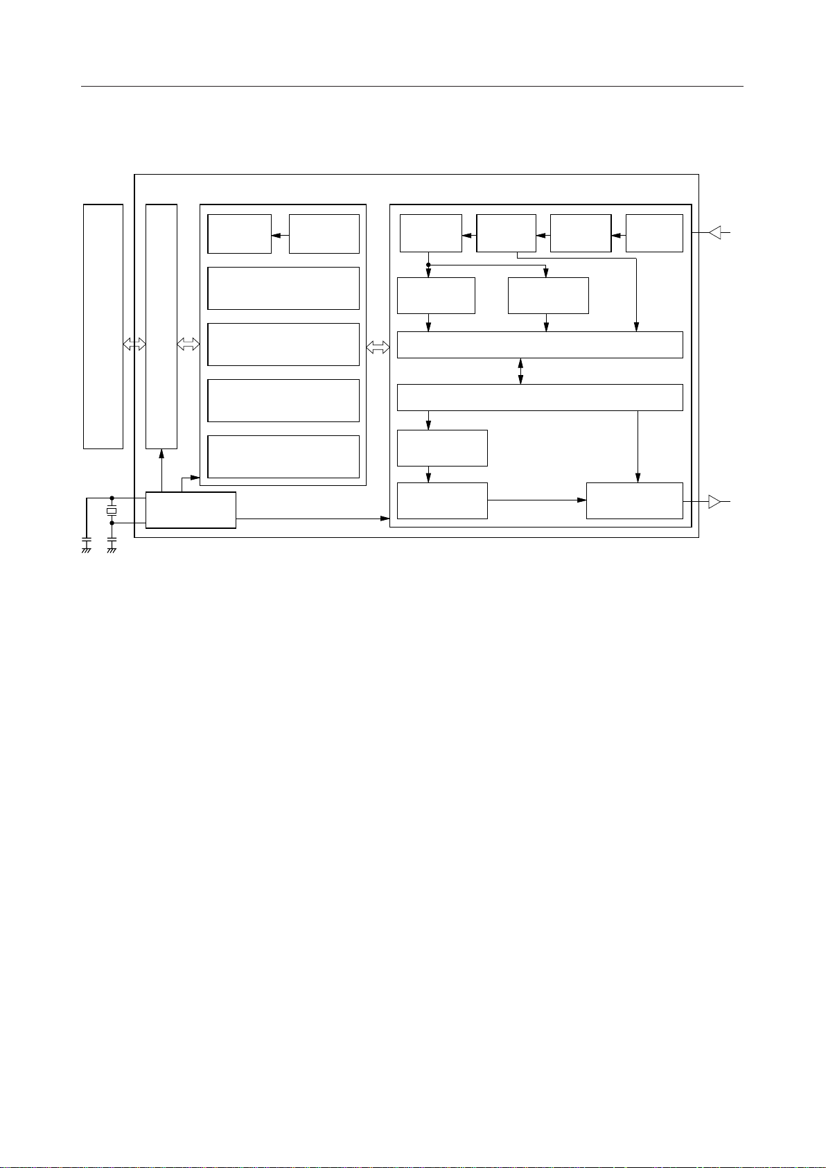
The MSM6636B is a transmission controller for automotive LAN based on data communication
protocol SAE-J1850. This device can realize a data bus topology bus LAN system with a PWM
bit encoding method (41.6 kbps). In addition to a protocol control circuit, MSM6636B has an
enclosed quartz oscillation circuit, host CPU interface (parallel interface), a transmit/receive
buffer, and a bus receiver circuit that decreases the burden on the host CPU.
FEATURES
• Based on SAE-J1850 CLASS B DATA COMMUNICATION NETWORK INTERFACE (issued
August 12, 1991)
• Non-destructive collision and priority control using CSMA/CD
• Internal transmit buffer (1 frame) and receive buffer (2 frames)
• Modulating/demodulating: PWM (Pulse Width Modulation)
• Transmission speed: 41.6 kbps
• Multi-address setting with physical addressing: 1 type / functional addressing: 15 types
• Address filter function by multi-addressing (broadcasting possible)
• Automatic retransmission function by arbitration loss and non ACK
• Three types of in-frame response support:
q Single-byte response from a single node
w Multi-byte response from a single node (with CRC code)
e Single-byte response from multiple nodes (ID response as ACK)
• Error detection by cyclic redundancy check (CRC)
• Various communication error detections
• Dual-wire bus abnormality detection by internal bus receiver and fault tolerance function
• Host CPU interface is accessed in parallel
• Sleep function
Low current consumption mode by oscillation stop (IDS Max < 50µA)
SLEEP / WAKE UP control from host CPU, WAKE UP via LAN bus
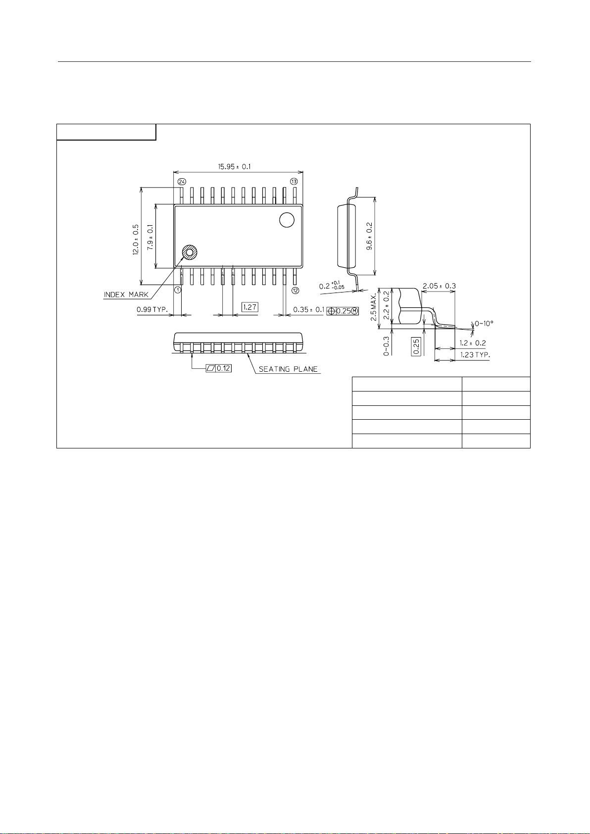
• Package: 24-pin plastic SOP (SOP24-P-430-1.27-K) (Product name : MSM6636BGS-K)
1/13
Page 2
¡ Semiconductor MSM6636B
BLOCK DIAGRAM
CPU
x'tal
Buffer Register
Receive
Register
Address Register
Status Register
Parallel Interface
Transmission Register
Response Register
Clock
Generator
Receive
Buffer
S-P
Converter
CRC
Checker
Generator
Converter
MSM6636B
CRC
P-S
LAN Controller
PWM
Decoder
Receive Controller
Transmission Controller
Degital
Filter
Address
Filter
Bus
Receiver
PWM
Encoder
LAN
Bus
Input
LAN
Bus
Output
2/13
Page 3
¡ Semiconductor MSM6636B
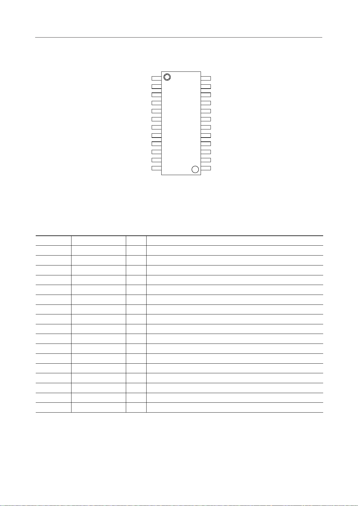
PIN CONFIGURATION (TOP VIEW)
24
23
22
21
20
19
AD3
18
17
16
15
14
13
DD
1
2
3
4
5
6
7
8
9
10
11
12
WR DV
RD AD7
ALE AD6
INT AD5
RES AD4
AV
BO– AD2
BI– AD1
BI+ AD0
BO+ CS
AGND OSC0
DGND OSC1
24-Pin Plastic SOP
PIN DESCRIPTION
Pin Description
Symbol
WR1I
RD2I
ALE3I
INT4O
RES5I
6—
AV
DD
BO–7O
BI–8I
BI+9I
BO+10 O
AGND11 —
DGND12 —
OSC113 O
OSC014 I
CS15 I
AD0-716-23 I/O
24 —
DV
DD
Type
Data write enable input pin
Data read enable input pin
Address latch input pin
Interrupt output pin
Reset input pin
Analog power supply voltage
LAN—BUS output –
LAN—BUS input –
LAN—BUS input +
LAN—BUS output +
Analog ground pin
Digital ground pin
Crystal (or ceramic resonator) oscillation output
Crystal (or ceramic resonator) oscillaiton input
Chip select input pin
Address input/data input-output pin
Digital power supply voltage
DD
3/13
Page 4

¡ Semiconductor MSM6636B
ABSOLUTE MAXIMUM RATINGS
DGND=AGND=0V
Parameter
Power Supply Voltage
Input Voltage
Output Voltage V
Power Dissipation P
Storage Temperature T
Symbol
DVDD, AV
V
I
O
D(SOP)
STG
DD
1
*
*1 24-pin SOP package power dissipation
Power Dissipation Curve
< 24-pin SOP package>
1000
[mW]
780
Condition Rating
—
AVDD=DV
AVDD=DV
DD
DD
–0.3 to +7.0
–0.3 to DVDD+0.3
–0.3 to DVDD+0.3
Ta=25°C 780
— –55 to +150
Unit
V
V
V
mW
°C
D(SOP)
500
–40 25 125 150
Power dissipation P
Ambient temperature Ta (°C)
4/13
Page 5

¡ Semiconductor MSM6636B
RECOMMENDED OPERATING CONDITIONS
DGND=AGND=0V
Parameter
Power Supply Voltage
Operating Frequency
Symbol
DVDD, AV
f
OSC
DD
Condition Range
AVDD=DV
DVDD=AVDD=5V±10%
DD
4.5 to 5.5
2 to 16
Ambient Temperature Ta — –40 to +85
Unit
V
MHz
°C
ELECTRICAL CHARACTERISTICS
DC Characteristics
DVDD=AVDD=5V±10%, DGND=AGND=0V, Ta=–40 to +85°C
Applied pin
Parameter Symbol Condition Unit
"H" Input Voltage
"L" Input Voltage
"H" Input Voltage
"L" Input Voltage
"H" Input Voltage
"L" Input Voltage
Receiver Hysteresis Width
"H" Input Current
"L" Input Current
"H" Input Current
"L" Input Current
"H" Input Current
"L" Input Current
"H" Output Voltage
"L" Output Voltage
"H" Output Voltage
"L" Output Voltage
GND Offset Voltage
Current Consumption 1
Current Consumption 2
V
IH1
V
IL1
V
IH2
V
IL2
V
IH3
V
IL3
V
H
I
IH1
I
IL1
I
IH2
I
IL2
I
IH3
I
IL3
V
OH1
V
OL1
V
OH2
V
OL2
V
OFF
I
DS
I
DD
—ADV
— A DGND–0.3 — DVDD ¥ 0.2 V
—EDV
— E DGND–1.0 — DGND ¥ 0.3 V
— B 2.4 — DVDD+0.3 V
— B –0.3 — 0.8 V
— E 100 — 400 mV
VI=V
DD
VI=0V B — — –1 mA
VI=V
DD
VI=0V
VI=V
DD
VI=0V BI (–) — — –100 mA
IO=–400µA C, AD0–7 DVDD–0.4 — — V
IO=+3.2mA C, AD0–7 — — DGND+0.4 V
IO=–4.0mA D DVDD–0.4 — — V
IO=+4.0mA D — — DGND+0.4 V
—
During sleep — *1 50 mA
f=16MHz,
no load
(see below
Min. Typ. Max.
for A-E)
¥ 0.8 — DVDD+0.3 V
DD
¥ 0.7 — DVDD+1.0 V
DD
B—— +1mA
RES — — +1 mA
RES
— — –100 mA
BI (+) — — +100 mA
———±1V
—
—
— — 10 mA
A: RES, CS
B: ALE, WR, RD, AD0-7
C: INT
D: BO–, BO+
E: BI–, BI+
*1 Typ.=0.2mA when V
=5V, f=16 MHz, Ta=25°C
DD
5/13
Page 6
¡ Semiconductor MSM6636B
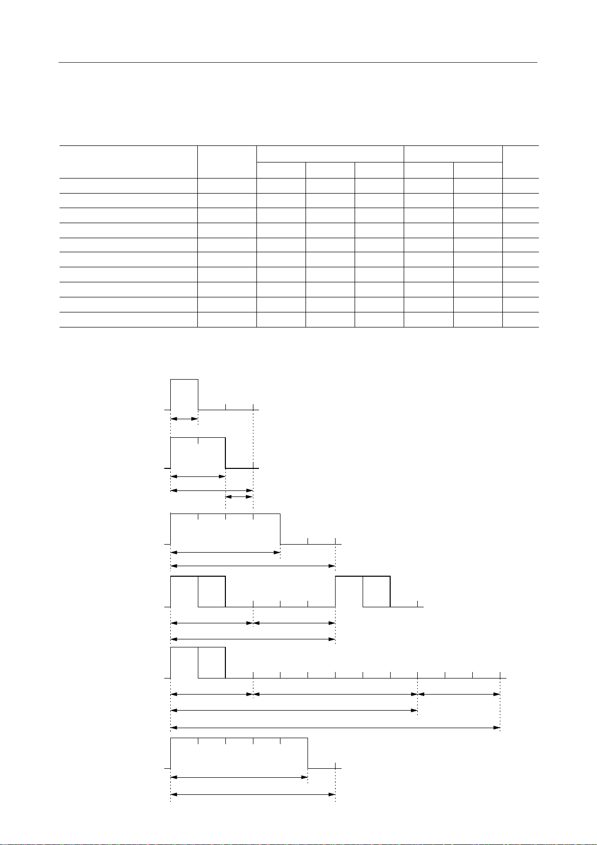
AC Chacteristics
• PWM bit timing
=AVDD=5V±10%, Ta=–40 to +85°C, In setting 41.6 kbps
DV
DD
Parameter Symbol
Bit Length TP1
"1" Dominant Width TP2
"0" Dominant Width TP3
"SOF" Dominant Width TP4
"SOF, BRK" Length TP5
"BRK" Dominant Width TP6
"EOD" + Bit Length TP7
"EOF" + Bit Length TP8
"EOF + IFS" " + Bit Length TP9 94.56 96.00 — 86.00 — ms
"0" Passive Width TP10
min typ max min max
23.64 24.00 24.36 21.00 28.00 ms
6.90 7.00 7.11 5.00 12.00 ms
14.87 15.00 15.23 13.00 20.00 ms
30.54 31.00 31.47 29.00 36.00 ms
47.28 48.00 48.72 45.00 52.00 ms
38.42 39.00 39.59 37.00 44.00 ms
47.28 48.00 48.72 43.00 51.00 ms
70.92 72.00 — 69.00 76.00 ms
8.86 9.00 9.14 4.00 15.00 ms
Transmit Receive
Unit
Note: The sending timing in the above table does not include the delay of the bus drivers.
" 1 "
" 0 "
" SOF "
" EOD "
" EOF "
" IFS "
Dominant
Passive
Dominant
Passive
Dominant
Passive
Dominant
Passive
Dominant
Passive
TP2
TP3
TP1
LAST BIT
LAST BIT
TP10
TP4
TP5
EOD
TP7
EOF IFS
TP8
" BRK "
Dominant
Passive
TP9
TP6
TP5
6/13
Page 7

¡ Semiconductor MSM6636B
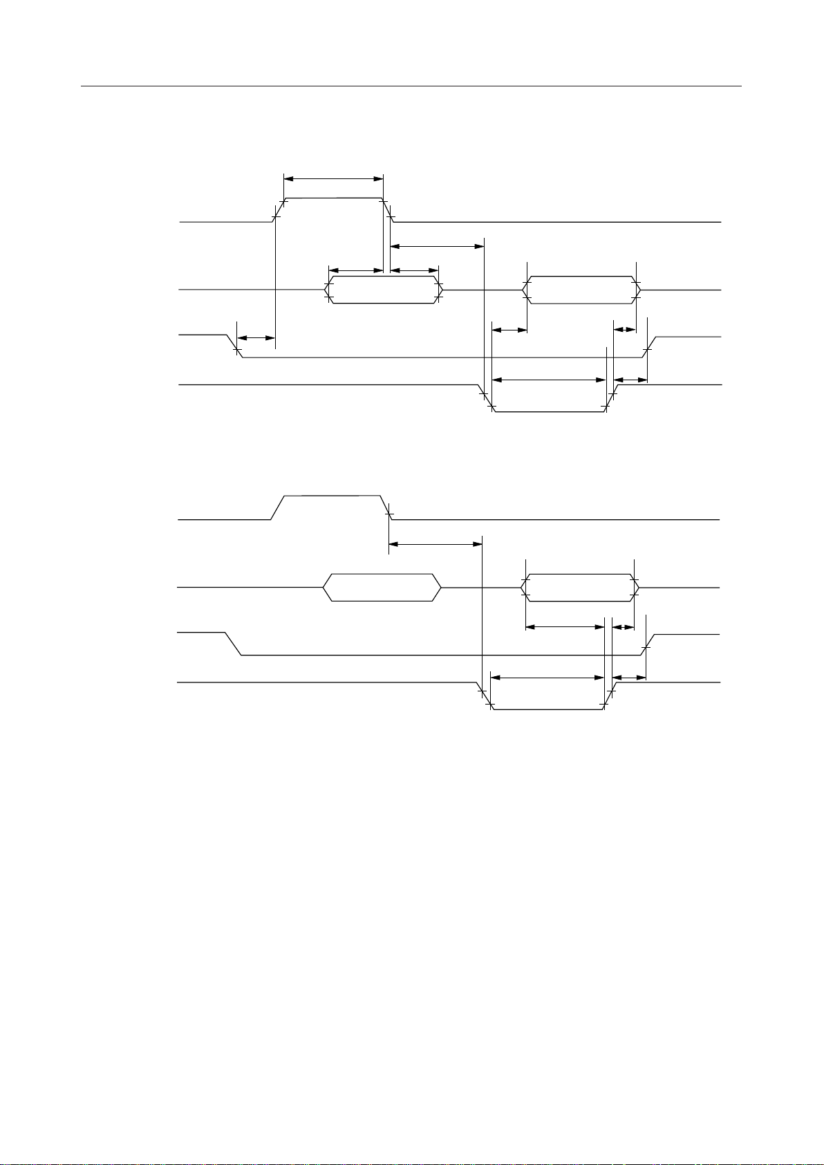
• CPU parallel interface timing
DVDD=AVDD=5V±10%, Ta=–40 to +85°C
Parameter Symbol Min. Max. Unit
ALE Pulse Width t
Address Setup Time t
Address Hold Time t
CS Setup Time t
RD Setup Time t
Continuous Read Cycle Time t
RD Output Enable Delay Time t
RD Output Floating Delay Time t
RD Pulse Width t
RD Hold Time at Read t
WR Setup Time
Continuous Write Cycle Time
t
WR Pulse Width
Data Setup Time
Data Hold Time
CS Hold Time at Write
t
AW
AS
AH
CSS
RDS
RDCY
RD
RDH
RDW
RCSH
t
WRS
WRCY
t
WRW
t
DS
t
DH
WCSH
Measuring
condition
=50pF
C
L
65 —
65 —
5—
50 —
20 —
160 —
—70
—50
75 —
0—
100 —
160 —
75 —
100 —
40 —
50 —
ns
7/13
Page 8
¡ Semiconductor MSM6636B
Parallel Interface Timing
t
AW
ALE
AD0-7
CS
RD
ALE
AD0-7
t
RDS
t
AS
t
AH
Address Data Output
t
t
CSS
RD
t
RDW
t
RDH
t
RCSH
Read Timing
t
WRS
Address Data Input
t
DS
t
DH
CS
WR
Write Timing
t
WRW
t
WCSH
8/13
Page 9
¡ Semiconductor MSM6636B
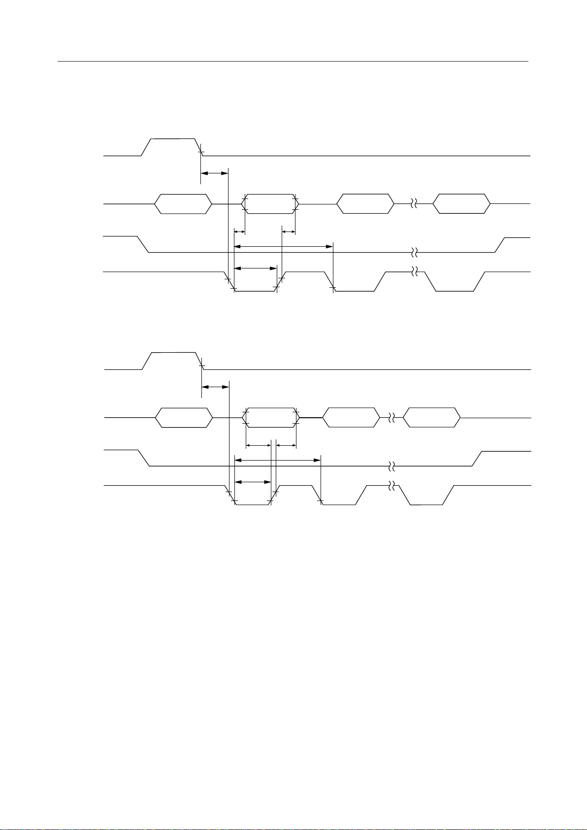
Timing When Automatic Address Increment is Used
ALE
AD0-7
CS
RD
ALE
AD0-7
CS
Address
Address
t
RDS
t
WRS
Data Output
t
RD
t
RDCY
t
RDW
Read Timing
Data Input
t
DS
t
WRCY
t
WRW
Data Output
t
Data Output
RDH
Data Input Data Input
t
DH
WR
Write Timing
9/13
Page 10
¡ Semiconductor MSM6636B
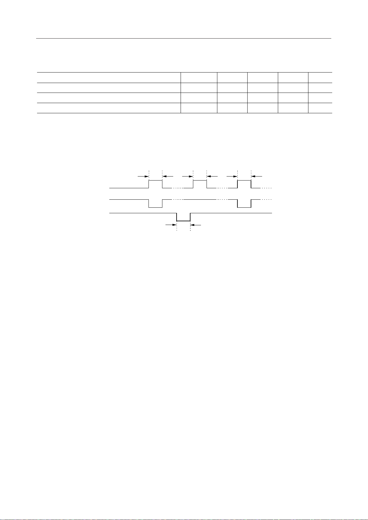
• Wakeup input signal
DV
=AVDD=5V±10%, Ta=–40 to +85°C
DD
Parameter Symbol Min. Typ. Max. Unit
LAN bus Passive Æ Dominant Change Pulse Width
RXD Terminal Input Pulse Width
Bus Receiver Stable Time *1
t
t
t
WD
WR
RS
7—ms
400 — ns
1—ms
—
—
—
*1 The stable time of the bus receiver is from just after wakeup to the restart of message
transmission and reception. However, the clock oscillation source should use an external
clock. (A clock is input even in the sleep status.)
t
WD
t
WD
t
WD
BI+
BI–
RXD
t
WR
Note: The time chart shows the wakeup input signals from each sleep status.
10/13
Page 11
¡ Semiconductor MSM6636B
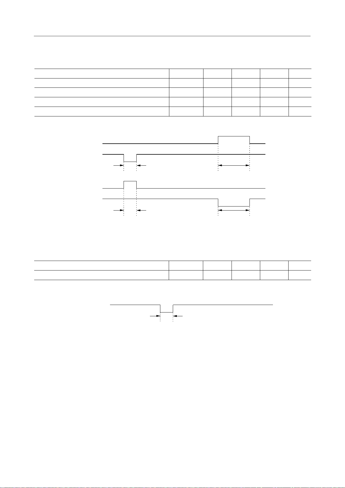
• Fault tolerant function operation conditions
DV
=AVDD=5V±10%, Ta=–40 to +85°C, In setting 41.6 kbps
DD
Parameter Symbol Min. Typ. Max. Unit
LAN bus (+) GND Short Circuit Detection Pulse Width
LAN bus (+) V
Short Circuit Detection Pulse Width
DD
LAN bus (–) GND Short Circuit Detection Pulse Width
LAN bus (–) V
Short Circuit Detection Pulse Width
DD
BUS(+)
BUS(–)
t
PG
BUS(+)
t
PG
t
PV
t
NG
t
NV
5—ms
48 — ms
—
—
48 — ms—
5—ms
—
t
PV
BUS(–)
t
NV
t
NG
• Reset input pulse width
=AVDD=5V±10%, Ta=–40 to +85°C
DV
DD
Parameter Symbol Min. Typ. Max. Unit
Reset Input Pulse Width t
RES
0.1 — ms
—
RES
t
RES
Note: The oscillation stable time after power ON is determined by the crystal used and the
parasitic capacitance generated by connection.
Make t
greater than or equal to the oscillation stable time.
RES
In the table above, the reset input pulse width indicates the minimum pulse width when
oscillation is stable after power is turned on.
11/13
Page 12
¡ Semiconductor MSM6636B
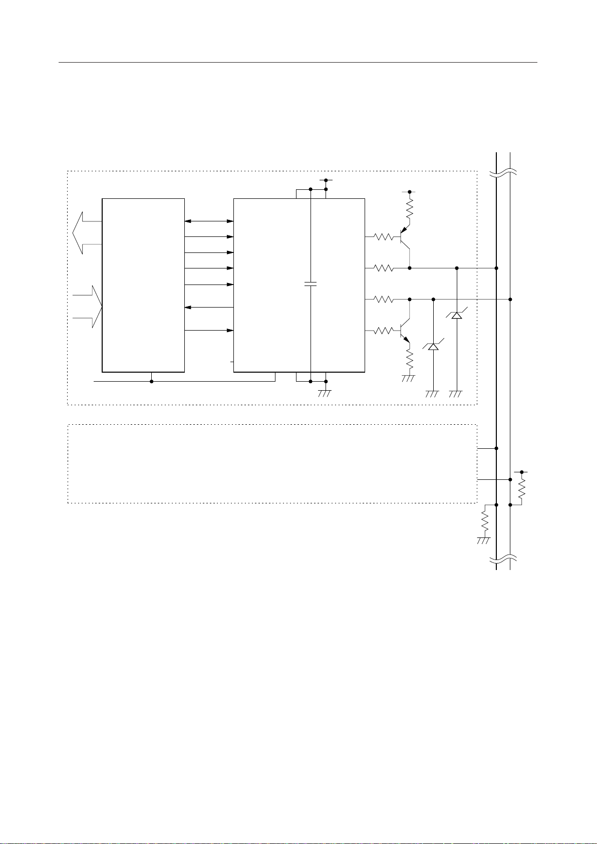
APPLICATION CIRCUIT
Host CPU and J1850 Line Bus Connection Example
Unit A
MSM6636BHost CPU
DV
DD
AD0-7 AD0-7
ALE ALE BO (+)
RD
WR WR BI (+)
PXX
INT
CLKOUT
OPEN
RD
CS
INT
OSC0
OSC1
RES
C
DGND
*1
AGNDRES
AV
DD
BI (–)
BO (–)
R
S
R
B
R
R
R
R
ZD
ZD
R
P
R
B
R
S
Unit B
R
.
D
.
.
Bus + Bus –
An optimum system can be constructed by selecting an optimum host CPU and combining it
with the MSM6636B.
*1 Insert a capacitor between the power supply and GND to prevent supply noise.
It is recommended to connect a small-capacitance bypass capacitor and a large-capacitance
filter capacitor serially. The typical capacitors are as follows:
0.01 to 0.22 mF : Ceramic capacitor
10 to 100 mF : Tantalum capacitor
12/13
Page 13
¡ Semiconductor MSM6636B
PACKAGE DIMENSIONS
(Unit : mm)
SOP24-P-430-1.27-K
Mirror finish
Package material
Lead frame material
Pin treatment
Solder plate thickness
Package weight (g)
Epoxy resin
42 alloy
Solder plating
5 mm or more
0.58 TYP.
Notes for Mounting the Surface Mount Type Package
The SOP, QFP, TSOP, SOJ, QFJ (PLCC), SHP and BGA are surface mount type packages, which
are very susceptible to heat in reflow mounting and humidity absorbed in storage.
Therefore, before you perform reflow mounting, contact Oki’s responsible sales person for the
product name, package name, pin number, package code and desired mounting conditions
(reflow method, temperature and times).
13/13
 Loading...