

Page 1

E2B0030-27-Y2
¡ Semiconductor
This version: Nov. 1997
Previous version: Mar. 1996
MSM6698¡ Semiconductor
MSM6698
80-DOT COMMON DRIVER
GENERAL DESCRIPTION
The MSM6698 is a dot matrix LCD common driver. Fabricated in CMOS technology, the device
consists of an 80-bit bi-directional shift register, 80-bit level shifter, and 80-bit 4-level driver.
The MSM6698 is equipped with 80 LCD output pins. By connecting more than two MSM6698s
in series, this LSI is applicable to a wide LCD panel.
FEATURES
• Logic supply voltage : 2.7 to 5.5 V
• LCD drive voltage : 18 to 28 V
• Applicable LCD duty : 1/64 to 1/240
• Interface with MSM6599B (80-dot segment driver)
• Package:
100-pin plastic QFP (QFP100-P-1420-0.65-K) (Product name: MSM6698GS-K)
1/8
Page 2
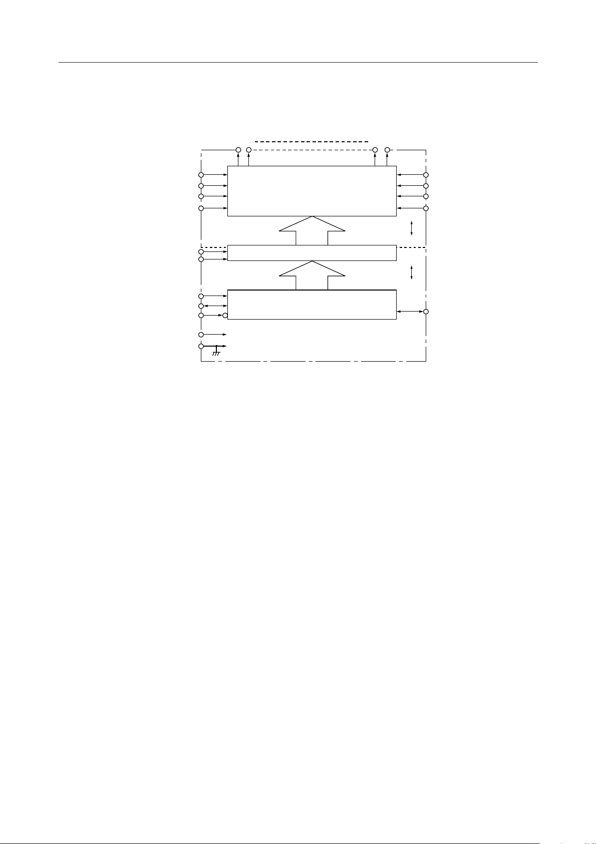
BLOCK DIAGRAM
MSM6698¡ Semiconductor
Note: V
DDR/L
O
O
2
1
V
1R
V
V
V
2R
5R
EER
DF
80-BIT 4-LEVEL DRIVER
80-Bit LEVEL SHIFTER
DISP OFF
SHL
IO
1
80-Bit BIDIRECTIONAL SHIFT REGISTER
CP
V
DDR/L
V
SS
indicates an abbreviation of V
DDR
and V
DDL
O
O
79
80
V
1L
V
2L
V
5L
V
DD
EE
DD
SS
IO
EEL
80
V
V
V
V
.
2/8
Page 3
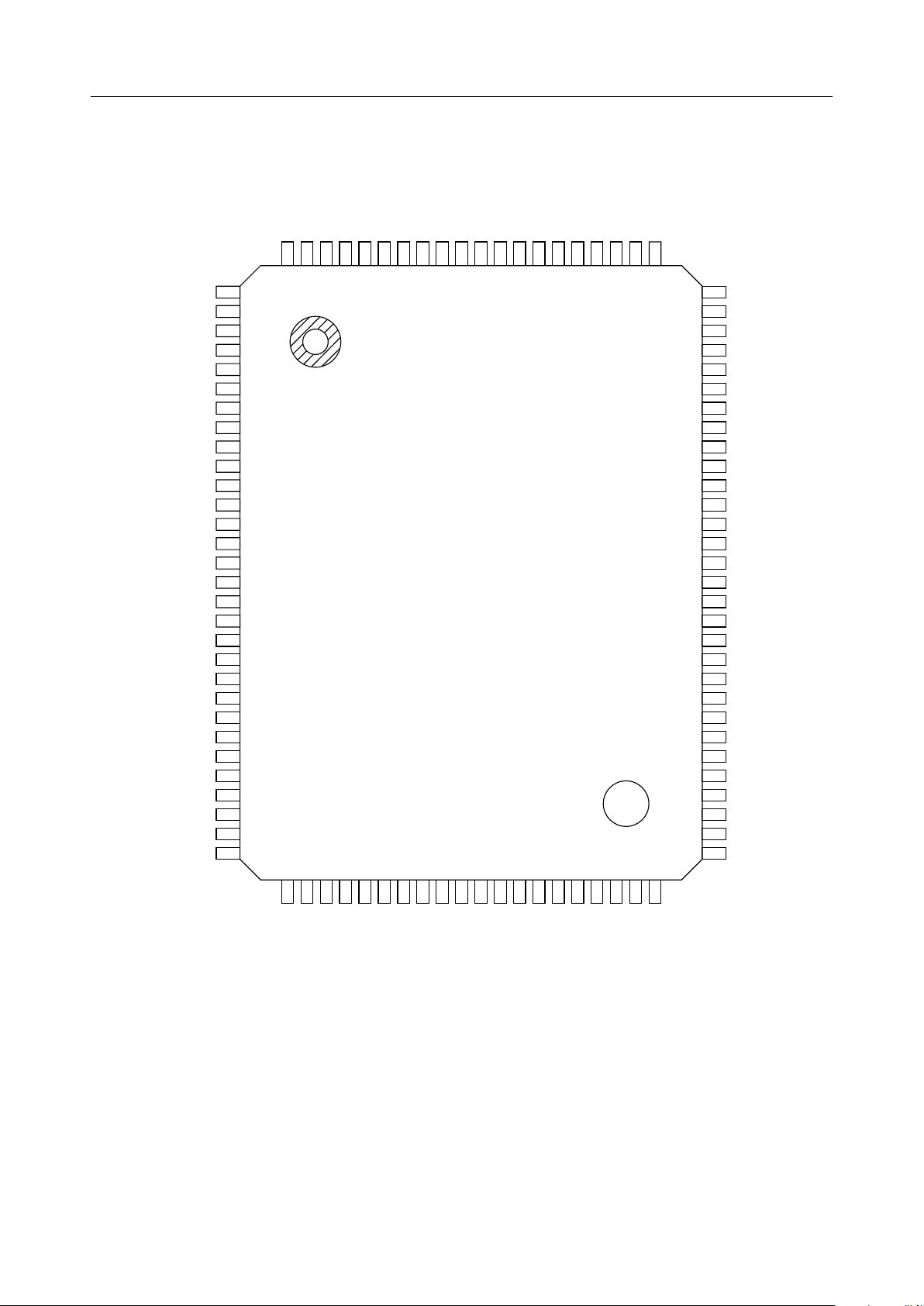
PIN CONFIGURATION (TOP VIEW)
MSM6698¡ Semiconductor
50
84
85
86
87
88
89
90
91
92
93
94
95
96
97
98
99
100
1
O
51
O
2
52
O
3
53
O
4
54
O
5
55
O
6
56
O
7
57
O
8
58
O
9
59
O
10
60
O
11
61
O
12
62
13
O
63
14
O
64
15
O
65
16
O
66
17
O
67
18
O
68
19
O
69
20
O
70
21
O
71
22
O
72
23
O
73
24
O
74
25
O
75
26
O
76
27
O
77
28
O
78
29
O
79
30
O
80
83
82
O31O32O33O34O35O36O37O38O39O40O41O42O43O44O45O46O47O48O49O
81
80
79
78
77
76
75
74
73
72
71
70
69
68
67
66
65
64
63
62
61
60
59
58
57
56
55
54
53
52
51
O
30
O
29
O
28
O
27
O
26
O
25
O
24
O
23
O
22
O
21
O
20
O
19
O
18
O
17
O
16
O
15
O
14
O
13
O
12
O
11
O
10
O
9
O
8
O
7
O
6
O
5
O
4
O
3
O
2
O
1
31
32
1L
EEL
V5LV2LV
V
DDL
V
NC
IO
80
DF
NC
CP
IO
1
NC
SS
V
SHL
DDR
V
V
EER
1R
5R
V
V2RV
50
49
48
47
46
45
44
43
42
41
40
39
38
37
36
35
34
33
DISP OFF
NC : No connection
100-Pin Plastic QFP
3/8
Page 4
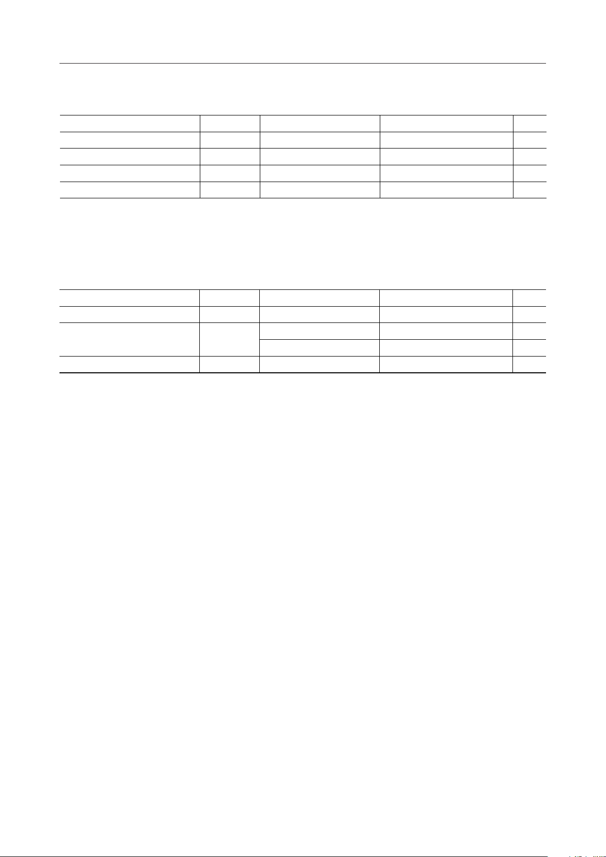
ABSOLUTE MAXIMUM RATINGS
Parameter Symbol Condition Rating Unit
Power Supply Voltage (1) V
Power Supply Voltage (2) V
Input Voltage V
Storage Temperature T
DD
–VEE *1 Ta = 25°C 0 to 30 V
DD
I
STG
MSM6698¡ Semiconductor
Ta = 25°C –0.3 to +6.5 V
Ta = 25°C –0.3 to VDD + 0.3 V
— –55 to +150 °C
*1 V1 > V2 > V5 > VEE, V
+ 10V ≥ V
EE
>VEE, V
5
DD
≥ V
V1 = V1R = V1L, V2 = V2R = V2L, V5 = V5R= V5L, VEE = V
RECOMMENDED OPERATING CONDITIONS
Parameter Symbol Condition Range Unit
Power Supply Voltage (1) V
Power Supply Voltage (2) V
Operating Temperature T
*1 V1 > V2 > V5 > VEE, V
EE
DD
–VEE *1
DD
op
+ 7V ≥ V
>VEE, V
5
V1 = V1R = V1L, V2 = V2R = V2L, V5 = V5R= V5L, VEE = V
— 2.7 to 5.5 V
No load 14 to 28 V
During LCD drive 18 to 28 V
— –20 to +75 °C
≥ V
DD
> V
1
> V
1
≥ V
2
EER
≥ V
2
EER
– 10V, VDD = V
DD
= V
EEL
– 7V, VDD = V
DD
= V
EEL
DDR
DDR
= V
= V
DDL
DDL
,
,
4/8
Page 5
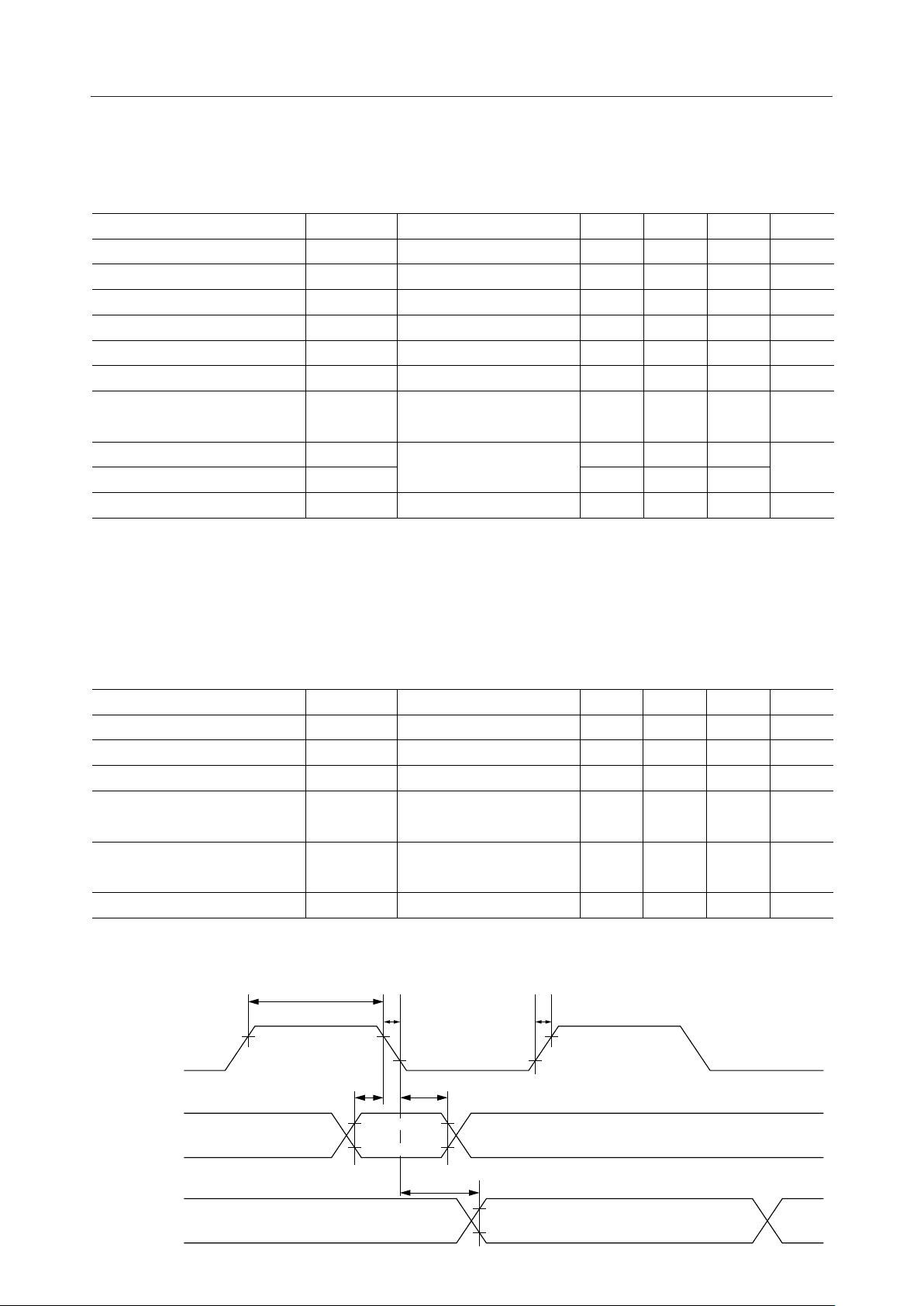
ELECTRICAL CHARACTERISTICS
DC Characteristics
Parameter Symbol Condition Min. Typ. Max. Unit
"H" Input Voltage V
"L" Input Voltage V
"H" Input Current I
"L" Input Current I
"H" Output Voltage V
"L" Output Voltage V
ON Resistance R
Logic Supply Current I
LCD Supply Current I
Input Capacitance C
IH
IL
IH
IL
OH
OL
ON
SS
EE
I
MSM6698¡ Semiconductor
(VDD = 2.7 to 5.5V, Ta = –20 to +75°C)
— 0.8V
—V
DD
SS
VI = VDD, VDD = 5.5V — — 1 mA*1
VI = 0V, VDD = 5.5V — — –1 mA*1
IO = –0.2mA, VDD = 2.7V VDD – 0.4 — — V*2
IO = 0.2mA, VDD = 2.7V — — 0.4 V*2
VDD – VEE = 25V
– VO | =0.25V
| V
N
fCP = 28kHz, VDD = 3.0V
– VEE = 25V, No load
V
DD
— — 2.0 kW*4
*3
——50
— — 300
f = 1MHz — — — pF
—VDDV*1
— 0.2V
DD
V*1
mA
*1 Applicable to CP, IO1, IO80, SHL, DF, DISP OFF.
*2 Applicable to IO1, IO80.
*3 VN = VDD to VEE, V2 = 1/16 (VDD – VEE), V5 = 15/16 (VDD – VEE), VDD = V1, VDD = 4.5V
VDD = V
*4 Applicable to O1 to O
Switching Characteristics
Parameter Symbol Condition Min. Typ. Max. Unit
"H", "L" Propagation Delay Time t
Clock Frequency f
CP Pulse Width t
Data Setup Time
(IO80) Æ CP
IO
1
Data Hold Time
CP Æ IO
Rise / Fall Time of CP t
(IO80)
1
DDR
= V
, V1 = V1R = V1L, V2 = V2R = V2L, V5 = V5R = V5L, VEE = V
DDL
80
(VDD = 2.7 to 5.5V, Ta = –20 to +75°C, CL = 15pF)
PLH
t
t
r (CP)
, t
CP
WCP
SETUP
HOLD
, t
PHL
f (CP)
———3ms
— — — 1 MHz
—
—
—
—
63——ns
100 — — ns
100 — — ns
——20ns
EER
= V
EEL
Note1: When display control by the DISPOFF pin is performed, CP rise and fall time must be
£ 1 ms.
t
WCP
t
f(CP)
t
r(CP)
IO
IO
CP
1
80
(IO80)
(IO1)
0.8V
DD
0.8V
DD
t
SETUP
0.8V
0.2V
DD
DD
0.2V
t
HOLD
t
PLH
0.8V
DD
DD
DD
0.2V
DD
DD
(t
)
PHL
0.8V
0.2V
5/8
Page 6
MSM6698¡ Semiconductor
FUNCTIONAL DESCRIPTION
Pin Functional Description
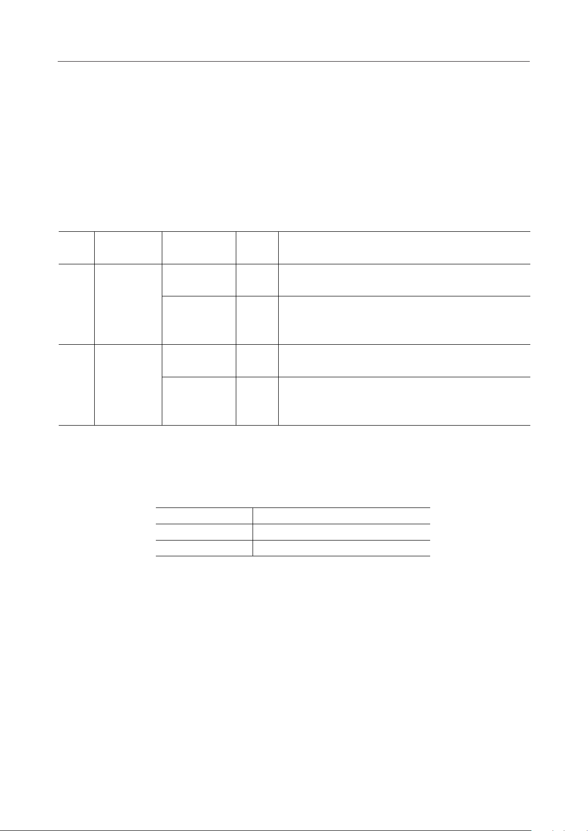
• IO1, IO80, SHL
IO1 and IO80 are I/O pins of the 80-bit bi-directional shift register. The shift direction can be
selected by the SHL pin. Set the SHL pin to "H" or "L" level during power-on. Table 1 gives
functions of IO1, IO80, and SHL.
Table 1
Shift Input,
I/O Pins
FunctionSHL
direction output
IO
1
O1 Æ
L
O
80
IO
80
Input
output
The scanning data from the LCD controller LSI is input into
synchronized with the clock pulse. *1
IO
1
Shift register contents output pin. The scanning data which
was input into IO
is output from IO80 with 80-bit delay,
1
synchronized with the clock pulse.
IO
80
O80 Æ
H
O
1
IO
1
Input
output
The scanning data from the LCD controller LSI is input into
synchronized with the clock pulse. *1
IO
80
Shift register contents output pin. The scanning data which
was input into IO
is output from IO1 with 80-bit delay,
80
synchronized with the clock pulse.
*1 The combination of the scanning data, IO1 or IO80, and the LCD driving output, O1 - O80, is
shown in the table below.
Scanning data LCD driving output
"H" Select level (V1, VEE)
"L" Non-Select level (V
, V5)
2
6/8
Page 7
MSM6698¡ Semiconductor
• CP
This is a clock pulse input pin of the 80-bit bidirectional shift register. Scan data is shifted at
the falling edge of a clock pulse.
• DF
This is an alternate signal input pin for LCD driving, which generally inputs a frame inversion
signal.
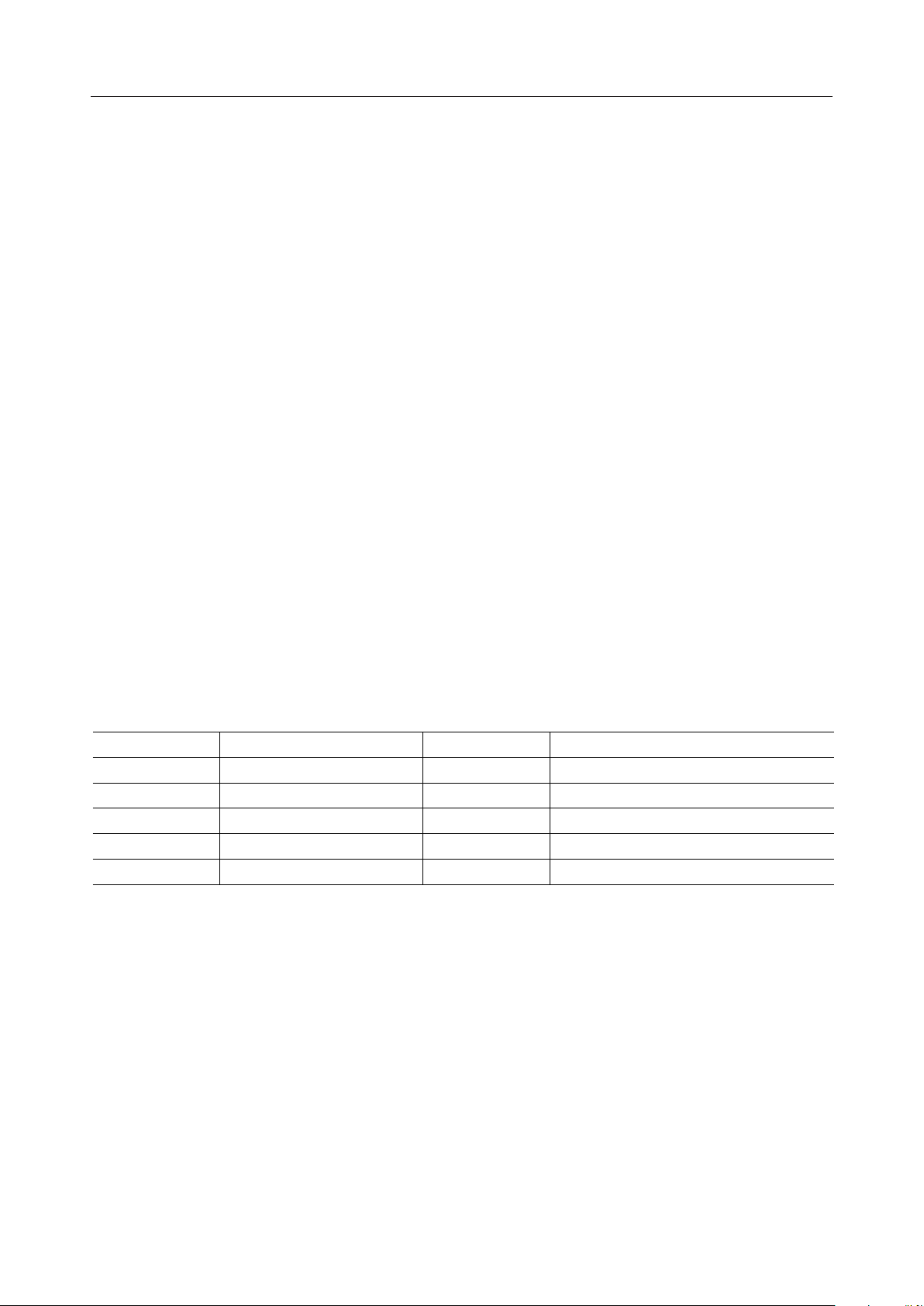
• DISP OFF
This is an input pin to control the output pins O1 to O80. During low signal input, signals on
the V1 level are output from the output pins O1 to O80. See the Truth Table.
• O1 to O
80
4-level driver outputs of this IC device, directly corresponding to each bit of the bidirectional
shift register. Any of four levels V1, V2, V5, and VEE is selected and output combining the DF
signal with shift register data (see the Truth Table).
These outputs are connected to the Common side on the LCD panel.
• V
DDR
, V
DDL
, V
SS
These are power supply pins of this IC. Both the V
DDR
and V
pins are normally 2.7 to 5.5
DDL
V. VSS is a grounding pin, which is normally 0 V.
• V1L, V2L, V5L, V
, V1R, V2R, V5R, V
EEL
EER
These are LCD drive bias voltage pins. The V1 pin may be separated from the VDD pin. Bias
power is supplied from an external source.
Truth Table
DF Shift register data DISP OFF Driver Output (O1 to O80)
LLH V
LHH V
HLH V
HHH V
¥¥LV
2
EE
5
1
1
¥ : Don't care
NOTES ON USE (when turning power ON and OFF)
The LCD drivers of this IC requires a high voltage. When a high voltage is applied to them with
the logic power supply floating, excess current flows. This may damage the IC. Be sure to carry
out the following power-ON and power-OFF sequences.
When turning power ON:
First turn on the logic circuits, then the LCD drivers, or turn on both of them at the same time.
When turning power OFF:
First turn off the LCD drivers, then the logic circuits, or turn off both of them at the same time.
7/8
Page 8
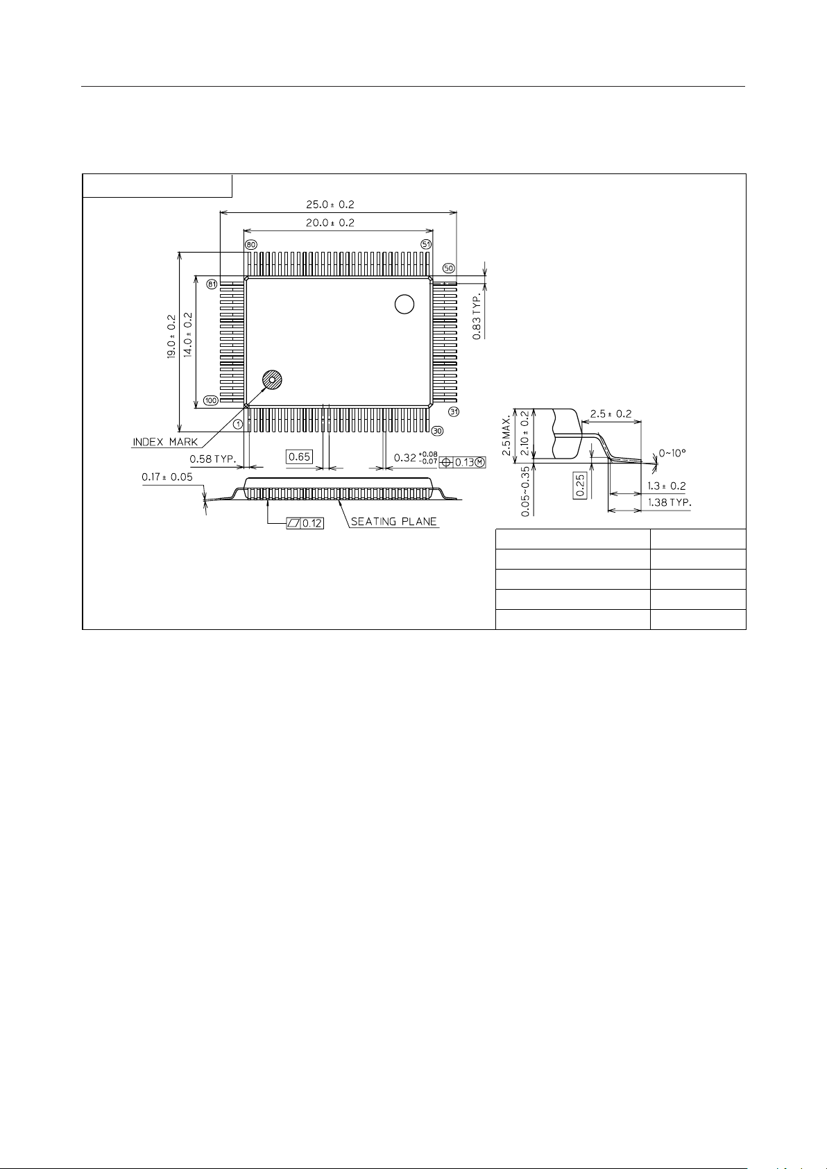
PACKAGE DIMENSIONS
QFP100-P-1420-0.65-K
Mirror finish
MSM6698¡ Semiconductor
(Unit : mm)
Package material
Lead frame material
Pin treatment
Solder plate thickness
Package weight (g)
Epoxy resin
42 alloy
Solder plating
5 mm or more
1.29 TYP.
Notes for Mounting the Surface Mount Type Package
The SOP, QFP, TSOP, SOJ, QFJ (PLCC), SHP and BGA are surface mount type packages, which
are very susceptible to heat in reflow mounting and humidity absorbed in storage.
Therefore, before you perform reflow mounting, contact Oki’s responsible sales person for the
product name, package name, pin number, package code and desired mounting conditions
(reflow method, temperature and times).
8/8
 Loading...