


E2E0013-38-93
This version: Sep. 1998
MSM6404A/6404VS¡ Semiconductor
¡ Semiconductor
Previous version: Mar. 1996
MSM6404A/6404VS
High speed and High performance 4-Bit Microcontroller
GENERAL DESCRIPTION
The MSM6404A microcontroller is a low-power device implemented in complementary metaloxide semiconductor technology. The MSM6404A is optimized for high-speed processing and
complicated-control applications.
The MSM6404VS is a CMOS 4-bit microcontroller that employs an external EPROM using a
piggy-back package in place of the program memory (ROM) internal to the MSM6404A.
The MSM6404VS can be used for program development verification because the programs can
be modified by programming an external EPROM 2732 equivalent or 2764A equivalent.
FEATURES
• Mask ROM (MSM6404A) : 4000 words ¥ 8 bits
External ROM (MSM6404VS) : 8196 words ¥ 8 bits
• RAM (including the stack area) : 256 words ¥ 4 bits
• I/O port
Input-output port : 8 ports ¥ 4 bits
Input port : 1 port ¥ 4 bits
4 bits are for input ports having a latch; the other 32 bits are input/output ports that allow
bit manipulation
• Three built-in counters : 12-bit time-base counter
12-bit programmable timer
8-bit high-speed programmable timer/event
counter
• Built-in 8-bit serial I/O register (with 3-bit counter)
• Five interrupts with five priority levels (4 internal, 1 external)
• 32 stacks (in RAM)
• Power-down features
• Minimum instruction execution time : 952 ns @ 4.2 MHz clock
• Instruction systems suitable for control
• Fully static operation
• Low power consumption
• Single 5 V supply
• Package options:
MSM6404A
42-pin plastic DIP (DIP42-P-600-2.54) : (Product name : MSM6404A-¥¥¥RS)
44-pin plastic QFP (QFP44-P-910-0.80-K) : (Product name : MSM6404A-¥¥¥GS-K)
44-pin plastic QFP (QFP44-P-910-0.80-2K) : (Product name : MSM6404A-¥¥¥GS-2K)
MSM6404VS
42-pin ceramic piggyback (ADIP42-C-600-2.54) : (Product name : MSM6404VS)
¥¥¥ indicates a code number.
1/25

2/25
MSM6404A/6404VS¡ Semiconductor
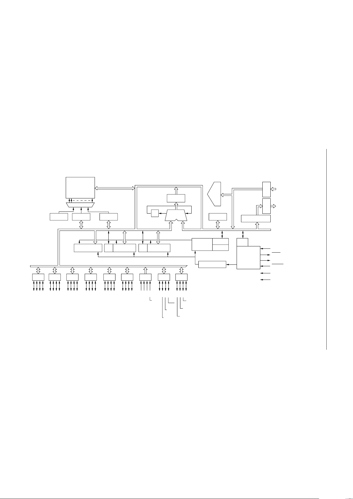
BLOCK DIAGRAM
MSM6404A
3210P83210P73210P63210P53210P43210P33210P23210P13210
P0
RAM
16 ¥ 16 ¥ 4 bits
DEC
HLSP
12-bit Timer 8-bit T/CP9 8-bit SRPA
C
ALU
ACC
INSTR
DEC
F
PC
PB
0
DEC
ROM
4000 ¥ 8 bits
Timing
&
Control
Interrupt
Control
PC INTE
PD IRQ
12-bit TBC
OSC
0
OSC
1
TEST
RESET
V
DD
GND
INT CIN
TMO
TCK
SCK, CTO, CLK
SI
SO
11
3/25
MSM6404A/6404VS¡ Semiconductor
BLOCK DIAGRAM (continued)
MSM6404VS
3210P83210P73210P63210P53210P43210P33210P23210P13210
P0
RAM
16 ¥ 16 ¥ 4 bits
DEC
HLSP
12-bit Timer 8-bit T/CP9 8-bit SRPA
C
ALU
ACC
INSTR
DEC
F
PC
PB
0
Timing
&
Control
Interrupt
Control
PC INTE
PD IRQ
12-bit TBC
OSC
0
OSC
1
TEST
RESET
V
DD
GND
INT CIN
TMO
TCK
SCK, CTO, CLK
SI
SO
12
RV
DV
I0 to I
7
A0 to A
12
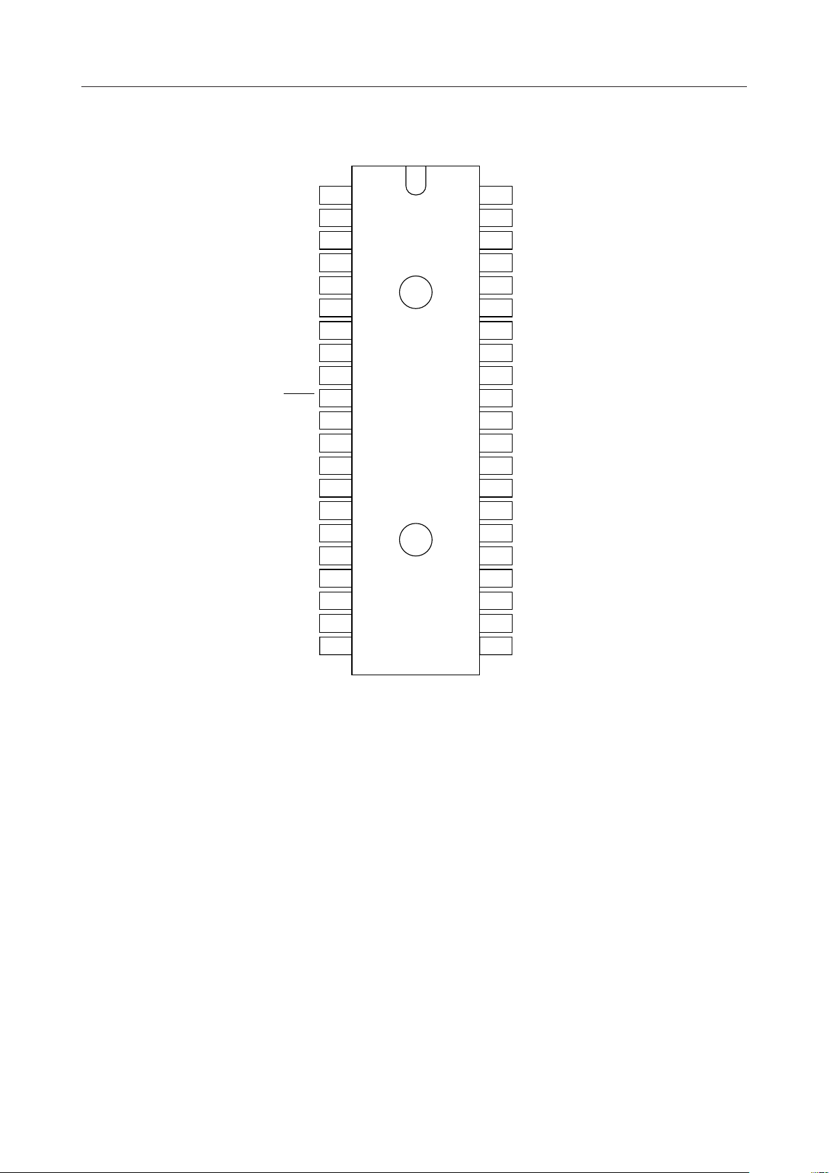
PIN CONFIGURATION (TOP VIEW)
MSM6404A/6404VS¡ Semiconductor
P4.0
P4.1
P4.2
P4.3
P3.0
P3.1
P3.2
P3.3
OSC
OSC
RESET
TEST
P2.0
P2.1
P2.2
P2.3
P0.0
P0.1
P0.2
P0.3
1
2
3
4
5
6
7
8
9
0
10
1
11
12
13
14
15
16
17
18
19
20
21GND P1.022
42
41
40
39
38
37
36
35
34
33
32
31
30
29
28
27
26
25
24
23
V
DD
P5.3
P5.2
P5.1
P5.0
P6.3
P6.2
P6.1
P6.0
P7.3
P7.2
P7.1
P7.0
P8.3
P8.2
P8.1
P8.0
P1.3
P1.2
P1.1
42-Pin Plastic DIP
4/25

PIN CONFIGURATION (TOP VIEW) (continued)
DD
P5.3
38
P5.2
37
P3.0
44
P4.3
43
P4.2
42
P4.1
41
P4.0
40
V
39
P5.1
36
P5.0
35
MSM6404A/6404VS¡ Semiconductor
P6.3
34
P3.1
P3.2
P3.3
OSC
OSC
RESET
TEST
P2.0
P2.1
P2.2
P2.3
1
2
3
4
0
5
1
6
7
8
9
10
11
12
13
14
15
16
17
18
19
20
21
22
P0.0
P0.1
P0.2
P0.3
GND
NC
P1.0
P1.1
P1.2
P1.3
P8.0
33
32
31
30
29
28
27
26
25
24
23
P6.2
P6.1
P6.0
NC
P7.3
P7.2
P7.1
P7.0
P8.3
P8.2
P8.1
NC: No-connection pin
44-Pin Plastic QFP
5/25

PIN CONFIGURATION (TOP VIEW) (continued)
MSM6404A/6404VS¡ Semiconductor
P4.0
P4.1
P4.2
P4.3
P3.0
P3.1
P3.2
P3.3
OSC
OSC
RESET
TEST
P2.0/INT
P2.1
P2.2
P2.3
P0.0
P0.1/SCK
P0.2/SO
P0.3/SI
GND
1
2
qVPP/V
wA12
DD
V
PGM/V
3
eA7
V
4
rA6
5
tA5
6
yA4
A11@3
7
uA3
OE/GND@2
8
iA2
9
0
oA1
10
1
!0A0
A10@1
CE/GND@0
11
!1I0
12
!2I1
13
!3I2
14
!4GND
15
16
17
18
19
20
21
@8
DD
@7
DD
@6
DD
A8@5
A9@4
I7!9
I6!8
I5!7
I4!6
I3!5
42
41
40
39
38
37
36
35
34
33
32
31
30
29
28
27
26
25
24
23
22
V
DD
P5.3
P5.2
P5.1
P5.0
P6.3
P6.2
P6.1
P6.0
P7.3
P7.2
P7.1
P7.0
P8.3
P8.2
P8.1
P8.0
P1.3
P1.2/TCK
P1.1/TMO
P1.0/CIN
42-Pin Ceramic Piggyback
6/25
MSM6404A/6404VS¡ Semiconductor
PIN DESCRIPTIONS
Symbol Type Description During reset
P0.0
P0.1/SCK
I/O "1"
P0.2/SO
P0.3/SI
P1.0/CIN
P1.1/TMO P1.1 is shared with timer output (TMO).
I/O
P1.2/TCK
P1.3
P2.0/INT
P2.1
I
P2.3
P3.0 to 3.3
P4.0 to 4.3
P5.0 to 5.3
P6.0 to 6.3
P7.0 to 7.3
I/O
I/O
I/O
I/O
I/O
I/O "0"P8.0 to 8.3
OSC
OSC
0
1
I Oscillation
O
P0.1 is shared with serial clock (SCK) input/output.
P0.2 is shared with serial data (SO) output.
P0.3 is shared with serial data (SI) input.
P1.0 is shared with counter input (CIN).
P1.2 is shared with timer clock input (TCK).
P2.0 is shared with external interrupt input (INT).
Input port with a latch, built-in pull-up resistorP2.2
—
8-bit output ports (at OPT instruction execution)
—
—
—
Crystal connection pins for clock oscillation
"1"
The latch is
reset.
"1"
"0"
"0"
"0"
waveform
TEST O Pulse output(Test pin for manufacturer)
RESET I
V
DD
—
Input pin for system reset
Power supply voltage pins
GND
Note: 1. The ports except for pins P2.0 to P2.3 are pseudo bidirectional ports.
2. When each port is used for output, the MSM6404A can drive one TTL (one input) and
the MSM6404VS can drive one LS TTL (one input).
Upper Pins for MSM6404VS
Symbol Type Description
A0 to A12
I0 to I7
CE/GND
DD
V
DD
GND
PP/VDD
—
—V
O
I
I
IOE/GND
IPGM/V
Address output
Data input
Chip enable input
Output enable input
Program input
Power supply voltage pins
Programed power supply voltage pin
—
—
7/25
ABSOLUTE MAXIMUM RATINGS (MSM6404A)
Parameter Symbol Condition Rating Unit
Power Supply Voltage V
Input Voltage V
Output Voltage V
DD
I
O
Ta = 25°C
Ta = 25°C per package
Power Dissipation P
Storage Temperature T
D
STG
Ta = 25°C per output 50 max. mW
— –55 to +150 °C
RECOMMENDED OPERATING CONDITIONS (MSM6404A)
Parameter Symbol Condition Range Unit
f
£ 1 MHz 3 to 6 V
Power Supply Voltage V
Data-Hold Voltage V
Operating Temperature T
Fan Out N
DD
DDH
op
OSC
£ 4.2 MHz
OSC
= 0 Hz
OSC
MOS load
TTL load 1
MSM6404A/6404VS¡ Semiconductor
–0.3 to +7 V
–0.3 to V
–0.3 to V
200 max. mW
4.5 to 5.5 Vf
–40 to +85 °C—
DD
DD
2 to 6 Vf
15
V
V
—
Note: Refer to the f
relation-ship between power supply voltage and operating frequency.
OSC-VDD
characteristic in OPERATING CHARACTERISTICS for the
8/25

MSM6404A/6404VS¡ Semiconductor
ELECTRICAL CHARACTERISTICS (MSM6404A)
DC Characteristics
(V
= 5 V ±10%, Ta = –40 to +85°C)
DD
Parameter Symbol Condition Min. Typ. Max. Unit
"H" Input Voltage*1, *2 V
"H" Input Voltage*3, *4 V
"L" Input Voltage V
"H" Output Voltage*1, *5 V
"L" Output Voltage*1
"L" Output Voltage*5
Input Current*3 I
Input Current*2, *4 — — 1/–30
"H" Output Current*1 I
"H" Output Current*1
Input Capacitance C
Output Capacitance C
Power Supply Current
(In Stop Mode)
V
V
IH/IIL
I
IH/IIL
OH
I
OH
I
DDS
IH
IH
IL
OH
OL
OL
O
I
f = 1 MHz, Ta = 25°C
V
= 2 V, no load, Ta = 25°C
DD
Crystal oscillation
Power Supply Current I
DD
f = 4.194304 MHz, no load
— 2.4 — V
— 3.6 — V
— –0.3 — +0.8 V
IO = –15 mA 4.2 — — V
IO = 1.6 mA — — 0.4 V
IO = 15 mA — — 0.4 V
VI = VDD/0 V — — 15/–15 mA
VI = VDD/0 V mA
VO = 2.4 V –0.1 — — mA
VO = 0.4 V — — –1.2 mA
—5—
—7—
— 0.2 5 mA
No load — 1 100 mA
—612mA
DD
DD
V
V
pF
*1 Applied to P0, P1, P3, P4, P5, P6, P7 and P8.
*2 Applied to P2.
*3 Applied to OSC0.
*4 Applied to RESET.
*5 Applied to OSC1.
9/25

AC Characteristics (MSM6404A)
Parameter Symbol Condition Min. Typ. Max. Unit
Clock (OSC
Cycle Time t
Input Data Setup Time t
Input Data Hold Time t
SR/TM Clock Pulse Width t
CT Clock Pulse Width
P2 Input Data Clock Pulse Width t
SR Data Setup Time t
SR Data Hold Time t
Data Delay Time t
Data Delay Time at Mode
Switching
Data Delay Time at OPT
Instruction
Data Delay Time at OPT
Instruction
CT/TM Data Delay Time Using
TBC Clock
SR/TM Data Delay Time Using
PORT Clock
CT Data Delay Time Using
PORT Clock
CT Data Delay Time Using
External Clock
SR/TM Data Delay Time Using
External Clock
SR Clock Invalid Time
INT Invalid Time
) Pulse Width tf
0
W
CY
DS
DH
WS/tWT
t
WC
WP
SS
SH
DR
t
DCR
t
DI1
t
DI2
t
CT/tTT
t
SR/tTR
t
CR
t
CP
t
SP/tTP
t
SINH
t
IINH
MSM6404A/6404VS¡ Semiconductor
(V
= 5 V ±10%, Ta = –40 to +85°C)
DD
— 119 — — ns
— 952 — — ns
— 120 — — ns
— 120 — — ns
— 120 — — ns
2/8 t
—
CY
+ 120
— 120 — — ns
— 120 — — ns
— 120 — — ns
CL = 15 pF — — t
CL = 15 pF — —
CL = 15 pF — —
CL = 15 pF — —
CL = 15 pF — —
CL = 15 pF — — tCY + 480 ns
CL = 15 pF — —
CL = 15 pF — —
CL = 15 pF — — 360 ns
— 2/8 t
— 1/8 t
CY
CY
——ns
+ 300 ns
CY
7/8 t
+ 300
6/8 t
+ 300
7/8 t
+ 300
2/8 t
+ 360
10/8 t
+ 480
2/8 t
+ 360
CY
CY
CY
CY
CY
CY
ns
ns
ns
ns
ns
ns
——ns
——ns
10/25

Timing Diagrams (MSM6404A)
Output Conditions
OSC
0
1MC
t
CY
MSM6404A/6404VS¡ Semiconductor
PA =
0, 1, 3
4, 5, 6
P0, P1, P3
P4, P5, P6
P7, P8
P0.1
P0.2
PA = 9 or A
P0.3
OPT INST.P4
OPT INST.P5
P0.1
P1.1
TBC clock
P0.2 P0.1 clock* SR
P1.1 P1.2 clock* TM
7 or 8
CT
TM
t
DR
t
DCR
t
DI1
t
DI2
t
CT
t
TT
t
SR
t
TR
P0.1 P1.0 clock* CT
P0.1 EXT clock
P1.0 P1.2 EXT clock
P0.1 CT
P0.2 SR
P1.1 TM
t
SP
t
TP
* Output data to port is clock for SR, TM or CT.
t
CR
t
CP
11/25

Input Conditions
OSC
P0, P1, P2
P3, P4, P5
P6, P7, P8
P0.1 SR clock
P1.2 TM clock
P2
MSM6404A/6404VS¡ Semiconductor
1MC
0
t
f
t
f
W
W
INPUT
DATA
t
t
DH
DS
t
WS
t
WT
t
WP
P1.0 CT clock
P0.1 SR clock
P0.3 SI
OSC
t
WC
INPUT
DATA
t
SStSH
1MC
0
t
IINH
t
SINH
t
IINH
t
SINH
: P0.1 (SR clock) INH period during LMSR INST.
(Note : P0.1 is used for clock of SR.)
: P2.0 (interrupt) INH period during RPB and RPBD INST.
12/25

)
Operating Characteristics (MSM6404A)
MSM6404A/6404VS¡ Semiconductor
Current (IOH) vs Voltage (VOH) for High State
Output
–1.0
–0.9
–0.8
–0.7
–0.6
(mA)
–0.5
OH
I
–0.4
–0.3
–0.2
–0.1
0
V
= 6 V
DD
5 V
4 V
3 V
12345678910
VOH (V)
Maximum Clock Frequency (f
Ta = 25°C Ta = 25°C
) vs Supply
OSC
Voltage (VDD)
10
9
8
7
6
(MHz)
5
OSC
f
4
3
2
1
0
12345678910
Ta = 25°C, CL =1 5 pF
VDD (V)
Current (IOL) vs Voltage (VOL) for Low State
Output
20
6 V
18
16
14
12
(mA)
10
OL
I
8
6
4
2
0
12345678910
3 V
V
4 V
VOL (V)
DD
= 5 V
Supply Current (IDD) vs Supply Voltage
(VDD)
10 m
1 m
100 m
(A)
DD
10 m
I
Ta = 25°C, no load
f
= 4 MHz
OSC
2 MHz
1 MHz
500 kHz
100 kHz
Maximum Clock Frequency (f
Temperature (Ta)
10
9
8
7
6
(MHz)
5
OSC
f
4
3
2
1
0
–40 –20 0 20 40 60 80 100120
Ta (°C
V
= 5 V
DD
) vs
OSC
CL = 15 pF
1 m
100 n
0 Hz
12345678910
0
VDD (V)
13/25

ABSOLUTE MAXIMUM RATINGS (MSM6404VS)
Parameter Symbol Condition Rating Unit
Power Supply Voltage V
Input Voltage V
Output Voltage V
DD
I
O
Ta = 25°C
Ta = 25°C per package
Power Dissipation P
Storage Temperature T
D
STG
Ta = 25°C per output 50 max. mW
— –55 to +150 °C
RECOMMENDED OPERATING CONDITIONS (MSM6404VS)
Parameter Symbol Condition Range Unit
f
£ 1 MHz 3 to 6 V
Power Supply Voltage V
Data-Hold Voltage V
Operating Temperature T
Fan Out N
DD
DDH
op
OSC
£ 4.2 MHz
OSC
= 0 Hz
OSC
MOS load
LSTTL load 1
MSM6404A/6404VS¡ Semiconductor
–0.3 to +7 V
–0.3 to V
–0.3 to V
200 max. mW
4.75 to 5.25 Vf
0 to +40 °C—
DD
DD
2 to 6 Vf
15
V
V
—
14/25

MSM6404A/6404VS¡ Semiconductor
ELECTRICAL CHARACTERISTICS (MSM6404VS)
DC Characteristics
(V
= 5 V ±5%, Ta = 0 to +40°C)
DD
Parameter Symbol Condition Min. Typ. Max. Unit
"H" Input Voltage*1, *2 V
"H" Input Voltage*3, *4 V
"L" Input Voltage V
"H" Output Voltage*1, *5 V
"L" Output Voltage*1
"L" Output Voltage*5
Input Current*3 I
Input Current*2, *4 — — 1/–30
"H" Output Current*1 I
"H" Output Current*1
Input Capacitance C
Output Capacitance C
Power Supply Current*6
(In Stop Mode)
V
V
IH/IIL
I
IH/IIL
OH
I
OH
I
DDS
IH
IH
IL
OH
OL
OL
O
I
f = 1 MHz, Ta = 25°C
V
= 2 V, no load, Ta = 25°C
DD
Crystal oscillation
Power Supply Current*6 I
DD
f = 4.2 MHz, no load
— 3.6 — V
— 3.6 — V
— –0.3 — +0.8 V
IO = –15 mA 4.2 — — V
IO = 0.4 mA — — 0.4 V
IO = 15 mA — — 0.4 V
VI = VDD/0 V — — 15/–15 mA
VI = VDD/0 V mA
VO = 2.4 V –0.1 — — mA
VO = 0.4 V — — –1.2 mA
—5—
—7—
—1 5mA
No load — 10 100 mA
—612mA
DD
DD
V
V
pF
*1 Applied to P0, P1, P3, P4, P5, P6, P7 and P8.
*2 Applied to P2.
*3 Applied to OSC0.
*4 Applied to RESET.
*5 Applied to OSC1.
*6 The EPROM current is not included.
15/25

AC Characteristics (MSM6404VS)
Parameter Symbol Condition Min. Typ. Max. Unit
Clock (OSC
Cycle Time t
Input Data Setup Time t
Input Data Hold Time t
SR/TM Clock Pulse Width t
CT Clock Pulse Width
P2 Input Data Clock Pulse Width t
SR Data Setup Time t
SR Data Hold Time t
Data Delay Time t
Data Delay Time at Mode
Switching
Data Delay Time at OPT
Instruction
Data Delay Time at OPT
Instruction
CT/TM Data Delay Time Using
TBC Clock
SR/TM Data Delay Time Using
PORT Clock
CT Data Delay Time Using
PORT Clock
CT Data Delay Time Using
External Clock
SR/TM Data Delay Time Using
External Clock
SR Clock Invalid Time
INT Invalid Time
) Pulse Width tf
0
W
CY
DS
DH
WS/tWT
t
WC
WP
SS
SH
DR
t
DCR
t
DI1
t
DI2
t
CT/tTT
t
SR/tTR
t
CR
t
CP
t
SP/tTP
t
SINH
t
IINH
MSM6404A/6404VS¡ Semiconductor
= 5 V ±5%, Ta = 0 to +40°C)
(V
DD
— 119 — — ns
— 952 — — ns
— 120 — — ns
— 120 — — ns
— 120 — — ns
2/8 t
—
CY
+ 120
— 120 — — ns
— 120 — — ns
— 120 — — ns
CL = 15 pF — — t
CL = 15 pF — —
CL = 15 pF — —
CL = 15 pF — —
CL = 15 pF — —
CL = 15 pF — — tCY + 480 ns
CL = 15 pF — —
CL = 15 pF — —
CL = 15 pF — — 360 ns
— 2/8 t
— 1/8 t
CY
CY
——ns
+ 300 ns
CY
7/8 t
+ 300
6/8 t
+ 300
7/8 t
+ 300
2/8 t
+ 360
10/8 t
+ 480
2/8 t
+ 360
CY
CY
CY
CY
CY
CY
ns
ns
ns
ns
ns
ns
——ns
——ns
16/25

Timing Diagrams (MSM6404VS)
Output Conditions
OSC
0
P0, P1, P3
P4, P5, P6
P7, P8
P0.1
P0.2
P1.1
OPT INST.P4
t
DI1
1MC
t
CY
t
DCR
MSM6404A/6404VS¡ Semiconductor
t
DR
P0.1/CTO
P1.1/TMO
P0.2/SO
P1.1/TMO
P0.1/CTO P1.0
EXT clock
EXT clock
P0.1
P1.0, P1.2
P0.1/CTO
P0.2/SO
P1.1/TMO
OPT INST.P5
TBC clock
P0.1 clock
P1.2 clock
clock
t
DI2
t
CT
t
TT
t
SR
t
TR
t
CR
t
CP
t
SP
t
TP
t
SINH
t
IINH
1MC
OSC
0
: P0.1/SCK inhibit period during LMSR INST.
: P2.0/INT inhibit period during RPB and RPBD INST.
t
SINH
t
IINH
17/25

Input Conditions
OSC
P0, P1, P2
P3, P4, P5
P6, P7, P8
P0.1 SR clock
P1.2 TM clock
P2
MSM6404A/6404VS¡ Semiconductor
1MC
0
t
f
t
f
W
W
INPUT
DATA
tDSt
DH
t
WS
t
WT
t
WP
P1.0 CT clock
P0.1/SCK
P0.3/SI
INPUT
DATA
t
SStSH
t
WC
18/25

Operating Characteristics (MSM6404VS)
MSM6404A/6404VS¡ Semiconductor
Current (IOH) vs Voltage (VOH) for High State
Output
–1.0
–0.9
–0.8
–0.7
–0.6
(mA)
–0.5
OH
I
–0.4
–0.3
–0.2
–0.1
0
Ta = 25°C, excluding pins A0-A
V
= 6 V
DD
5 V
4 V
3 V
12345678910
VOH (V)
Maximum Clock Frequency (f
OSC
12
) vs Supply
Voltage (VDD)
10
9
8
7
6
(MHz)
5
OSC
f
4
3
2
1
0
12345678910
Ta = 25°C, CL = 15 pF
VDD (V)
Current (IOL) vs Voltage (VOL) for Low State
Output
V
DD
Ta = 25°C
= 6 V
20
18
16
14
12
(mA)
10
OL
I
8
6
4
2
0
3 V
12345678910
5 V
4 V
VOL (V)
Supply Current (IDD) vs Supply Voltage
(VDD)
10 m
500 m
100 m
50 m
(A)
DD
10 m
I
5 m
1 m
5 m
Ta = 25°C, no load,
excluding EPROM current
f
= 4 MHz
OSC
2 MHz
1 MHz
500 kHz
100 kHz
0 Hz
Maximum Clock Frequency (f
Temperature (Ta)
V
= 5 V, CL = 15 pF
10
9
8
7
6
(MHz)
5
OSC
f
4
3
2
1
0
–40 –20 0 20 40 60 80 100120
DD
Ta (°C)
OSC
) vs
1 m
500 n
100 n
0
12345678910
VDD (V)
19/25

FUNCTIONAL DESCRIPTION
MSM6404VS Interface to EPROM
EPROM insertion method
2732 2764A
2732 EPROM 2764A EPROM
EPROM read timing
MSM6404A/6404VS¡ Semiconductor
1MC
T1 T2 T3 T4 T1
OSC
0
tfWt
fW
A
0 to A12
Address
CE, OE
I
0 to I7
Use EPROM with t
of less than 357 ns.
ACC
t
ACC
Read Data
Read data is read into the instruction register in the first half of the T1 state.
20/25

Differences between MSM6404A and MSM6404VS (PIGGYBACK)
Item MSM6404A MSM6404VS (Piggyback)
1. Ports P0, 1, 3 are set to "1" and ports P2, 4,
Port
initialization
during reset
2. Timer
operation
3. Shift register
5, 6, 7, 8 are reset to "0" directly by the reset
input signal.
After being reset, the timer continues to stop
until data is set in it.
Serial out F/F (SOF/F) is set to "0" after being
reset.
4.
Internal clock Internal clockPort
input/output
timing
Input
Data are input
at this time.
Ports P0, 1, 3 are set to "1" and ports P2, 4,
5, 6, 7, 8 are initialized during reset cycle.
It is undefined whether the timer starts or
not after being reset. Therefore, the timer
should be initialized by software.
It is undefined whether serial out F/F
(SOF/F) is "0" or "1" after being reset.
Therefore the serial out F/F should be
initialized by software.
Input
MSM6404A/6404VS¡ Semiconductor
Data are input
at this time.
Port
5.
input/output
characteristics
6.
capacity
7.
instruction
Internal clock
Output
Synchronized
with falling edge
Data are output
at this time.
TTL FO = "1"
(I
= 1.6 mA @ 0.4 V)
OL
V
DD
P2.0-3 P2.0-3
TTL compatible input CMOS input
P0.0-P8.3 P0.0-P8.3
(Except P2.0-3) (Except P2.0-3)
Up to 4 Kbytes Up to 8 Kbytes accessible Available ROM
Not available AvailableLJP a13, LCAL a
13
Internal clock
Output
LSTTL FO = "1"
(I
= 0.4 mA @ 0.4 V)
OL
Data are output
at this time.
VDD V
DD
21/25

PACKAGE DIMENSIONS
DIP42-P-600-2.54
MSM6404A/6404VS¡ Semiconductor
(Unit : mm)
Package material
Lead frame material
Pin treatment
Solder plate thickness
Package weight (g)
Epoxy resin
42 alloy
Solder plating
5 mm or more
6.20 TYP.
22/25

QFP44-P-910-0.80-K
Mirror finish
MSM6404A/6404VS¡ Semiconductor
(Unit : mm)
Package material
Lead frame material
Pin treatment
Solder plate thickness
Package weight (g)
Epoxy resin
42 alloy
Solder plating
5 mm or more
0.35 TYP.
Notes for Mounting the Surface Mount Type Package
The SOP, QFP, TSOP, SOJ, QFJ (PLCC), SHP and BGA are surface mount type packages, which
are very susceptible to heat in reflow mounting and humidity absorbed in storage.
Therefore, before you perform reflow mounting, contact Oki’s responsible sales person for the
product name, package name, pin number, package code and desired mounting conditions
(reflow method, temperature and times).
23/25

QFP44-P-910-0.80-2K
Mirror finish
MSM6404A/6404VS¡ Semiconductor
(Unit : mm)
Package material
Lead frame material
Pin treatment
Solder plate thickness
Package weight (g)
Epoxy resin
42 alloy
Solder plating
5 mm or more
0.41 TYP.
Notes for Mounting the Surface Mount Type Package
The SOP, QFP, TSOP, SOJ, QFJ (PLCC), SHP and BGA are surface mount type packages, which
are very susceptible to heat in reflow mounting and humidity absorbed in storage.
Therefore, before you perform reflow mounting, contact Oki’s responsible sales person for the
product name, package name, pin number, package code and desired mounting conditions
(reflow method, temperature and times).
24/25

42-PIN CERAMIC PIGGYBACK ADIP42-C-600-2.54
MSM6404A/6404VS¡ Semiconductor
(Unit : mm)
25/25
 Loading...