OKI MSM63V89CTS-K Datasheet

E2D0034-39-21
¡ Semiconductor MSM63V89C
¡ Semiconductor
This version: Feb. 1999
Previous version: May. 1997
MSM63V89C
1,048,576-Word x 1-Bit Solid-State Recorder Data Register
GENERAL DESCRIPTION
The MSM63V89C is a solid-state recorder data register in 1,048,576 words x 1 bit configuration.
The MSM63V89C has a built-in internal address generator circuit allowing continuous serial read/
write operation by single external clock input. The internal address is automatically incremented by
one by read/write operation.
Address designation in units of 1024 words in the direction of words is possible by an external
serial address input.
The built-in refresh timer and refresh counter have eliminated the need of an external refresh circuit
and realized a low power consumption.
26/20-pin plastic TSOP is used as the package and the operating temperature range is between 0°C
and 70°C.
The MSM63V89C is suitable for storing large capacity data with battery backup. A solid state
recording and playback system can easily be constructed in combination with OKI’s voice synthesizer
ICs.
FEATURES
• Configuration: 1,048,576 x 1 bit
• Serial access operation:
Serial access time 1.5 ms (3.0 ms)
Serial read/write cycle time 2.0 ms (4.0 ms)
Fast mode read/write cycle time 0.4 ms (0.4 ms)
Times in parentheses indicate ones in self-refresh mode.
• Low current consumption: 50 mA max. (for data holding, VCC=3.0 V)
• Wide operating supply voltage range: Single 2.7 to 3.6V
• Auto-refresh/self-refresh changeable
• Package:
26/20-pin plastic TSOP (TSOPII26/20-P-300-1.27-K) (Product name: MSM63V89CTS-K)
1/10

¡ Semiconductor MSM63V89C
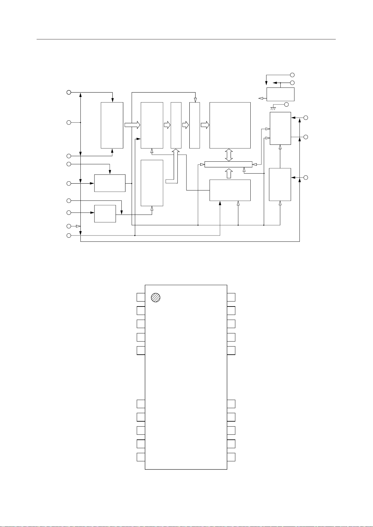
BLOCK DIAGRAM
TEST
V
CC
SAD
CS
SAS
FAM
RWCK
RFSH
RS/A
TEST
TAS
Sin
Address
Register
Clock
Timing
Generator
Refresh
Timer
Pout
X-address
Counter
Load
Clock
Refresh
Counter
Clock
Multiplexer
Address
X-decoder/
Driver
Data Register
Y-decoder/sense Amp
Y-address Counter
Reset Clock
1,048,576
V
BB
Generator
I/O
Controller
Write
Clock
Generator
V
SS
D
IN
D
OUT
WE
PIN CONFIGURATION (TOP VIEW)
1D
IN
2WE
3TEST
4NC
5CS
9SAD
10NC
11SAS
12TAS
26 V
SS
25 D
OUT
24 TEST
23 NC
22 NC
18 RWCK
17 NC
16 FAM
15 RFSH
13V
CC
NC : No connection
26/20-pin plastic TSOP
14 RS/A
2/10

¡ Semiconductor MSM63V89C
PIN DESCRIPTIONS
Pin
1
Symbol
D
IN
WE
TEST
CS
SAD
SAS
TAS
V
CC
RS/A
RFSH
FAM
RWCK
D
OUT
V
SS
Description
Data input
Write enable2
Test input3, 24
Chip select5
Serial address data9
Serial address strobe11
Transfer address strobe12
Power supply (3.3 V)13
Auto-Refresh/Self-Refresh Select14
Refresh Clock Input15
Fast Access Mode Select16
Read/write clock18
Data output25
Ground (0 V)26
3/10

¡ Semiconductor MSM63V89C
ABSOLUTE MAXIMUM RATINGS
Parameter Symbol Condition Rating Unit
Terminal Voltage V
Output Short-Circuit Current I
Power Dissipation P
Operating Temperature T
Storage Temperature T
T
OS
D
op
STG
Ta = 25°C, relative to V
Ta = 25°C 50 mA
Ta = 25°C 1 W
— 0 to 70 °C
— –55 to +150 °C
SS
–1.0 to +7.0 V
RECOMMENDED OPERATING CONDITIONS
(Ta = 0 to 70°C)
Parameter Symbol Min. Typ. Max. Unit
Supply Voltage V
Supply Voltage V
"H" Input Voltage
"L" Input Voltage
CC
SS
V
IH
V
IL
2.7 3.3 3.6 V
000V
VCC – 0.5 V
CC
V
+ 0.5 V
CC
–0.5 0 +0.5 V
ELECTRICAL CHARACTERISTICS
DC Characteristics
Parameter Symbol Condition Min. Max. Unit
"H" Output Voltage V
"L" Output Voltage V
Input Leakage Current I
Output Leakage Current I
Supply Current (in operating state) I
Supply Current (in standby state) I
Supply Current (FAM) I
OH
OL
LI
LO
CC1
CC2
CC3
V
V
CC
CC
(VCC = 2.7 V to 3.6 V, Ta = 0 to 70°C)
I
= –0.5 mA V
OH
I
= 0.5 mA — 0.4 V
OL
V
= 0 V to V
I
V
= 0 V to V
O
= 3 V, t
V
CC
= 3 V, t
CC
CC
= 2 µs — 3 mA
RWC
= 3 V — 50 mA
= 0.4 ms — 10 mA
RWC
– 0.5 — V
CC
–1 +1 mA
–1 +1 mA
4/10
 Loading...