OKI MSM62X42B Datasheet

¡ Semiconductor MSM62X42B
¡ Semiconductor
MSM62X42B
REAL TIME CLOCK IC WITH BUILT-IN CRYSTAL
DESCRIPTION
The MSM62X42B is a bus-connection Microcomputer peripheral IC of a Real Time Clock
with built-in crystal in the perpetual calendar
which can be read and written from a second
unit. The interface between this IC and a
microcomputer uses 4 data buses, 4 address
buses, 3 control buses and 2 chip selects and
carries out setting up, amending and reading
time.
ALE input is available for 8048 system, 8051
system or 8085 system and is used for other
microcomputers if this input is fixed at "H".
FEATURES
• 32.768kHz built-in crystal oscillator
(2 ranks of ±10PPM and ±50PPM --DIP)
(2 ranks of ±20PPM and ±50PPM --SOP)
• Real time clock of second, minute, date,
month, year and day of week
• Interface corresponding to microcomputer bus
• 30-second compensation controlled by
software
• Periodical interrupt function (or
periodical waveform output) for alarm
The clock function provides seconds, minutes, hours, day of week, date, month, year,
12/24 hour selectable, automatic leap year in
the Christian Era and 30-second compensation controlled by software. The periodical
interrupt function (or periodical waveform
output) and the STOP/START function of the
clock are also provided. The device is a silicon
gate CMOS and the current consumption is
low. The built-in crystal oscillator is 32.768
kHz and battery backup operation is considered.
• STOP/START function for clock
• 12/24 hour selectable
• AEL input for 8048 system, 8051 system
or 8085 system (when a microcomputer
does not provide the ALE output, fix the
AEL input at "H".)
• Low current consumption for CMOS
device
• Low STANDBY voltage and small
STANDBY current
• 18-pin plastic DIP(DIP18-P-300)
• 24-pin plastic SOP
PIN CONFIGURATION
MSM62X42BRS
(TOP View) 18 Lead Plastic DIP
1
STD.P
2
CS
0
ALE
3
4
A
0
5
A
1
6
A
2
A
7
3
8
RD D
910
GND
Note: The actual type name indicates the abbreviated one, M62X42B.
MSM62X42BGS-1K
(TOP View) 24 Lead Plastic SOP
1
18
V
DD
17
(VDD)
16
)
(V
DD
15
CS
1
14
D
0
13
D
1
D
12
2
11
3
WR
STD.P
2
CS
0
3
NC
4
ALE
5
A0
6
NC
7
A
1
8
NC
9
A
2
10
A
3
11
RD
12
GND WR
NC : NO CONNECTION (unused pins)
24
V
DD
(VDD)
23
(V
)
DD
22
21
NC
20
CS
1
19
0
D
18
NC
17
NC
16
D
1
15
D
2
14
D
3
13
41
RANK
¡ SemiconductorMSM62X42B
M62X42B
JAPAN xxxxA
Lot no. Stability A or B
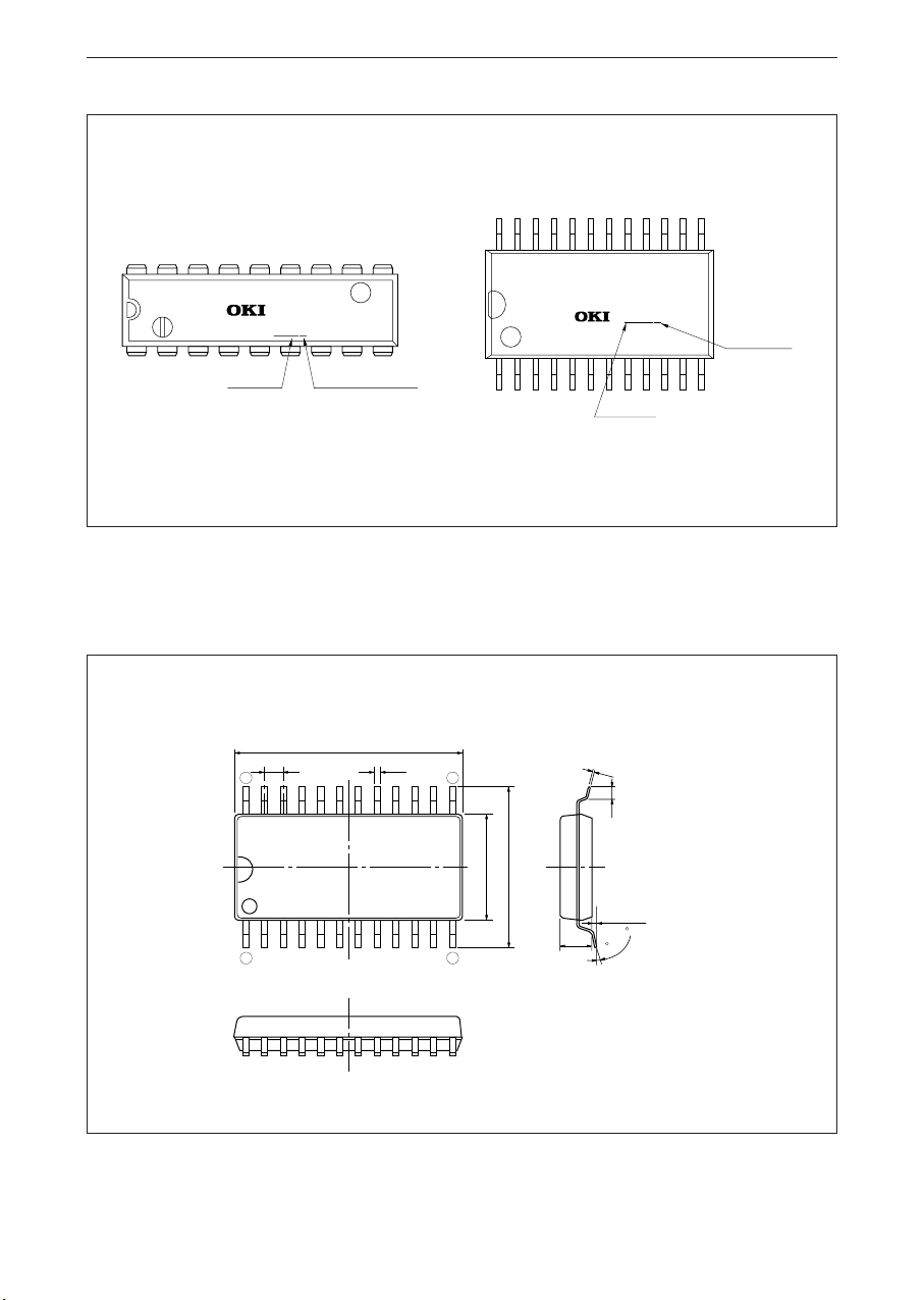
EXTERNAL DIMENSION
1.27 0.35
24 13
A: 10PPM
B: 50PPM
16.3 MAX
M62X42B
xxxxS
Stability S or B
±
S: 20PPM
±
B: 50PPM
±
±
Lot no.
(UNIT : mm)
0.2
1.0
42
8.0MAX
12.2MAX
0.3MAX
10
2.58
~
0
1
12
MAX
¡ Semiconductor MSM62X42B
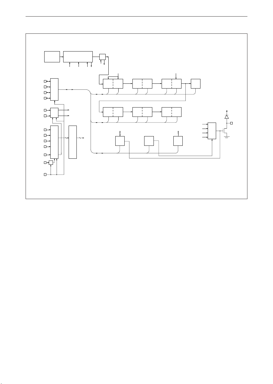
FUNCTION BLOCK DIAGRAM
CS
ALE
CS
D
D
D
D
WR
RD
A
A
A
A
3
2
1
0
3
2
1
0
32.768kHz
0
1
X'tal
OSC
&
T
E
COUNTER
RESET
STOP
bit
bit
G
A
T
E
G
A
G
A
T
E
&
L
A
T
C
H
D
E
C
O
D
E
R
1Hz
30 sec ADJ
bit
S
1
~
C
F
HOLD
bit
BUSY
bit
30 sec ADJ bit
S
1S10
D
1D10
MI1MI
10
MO1MO
10
C
D
C
E
* S1 ~ W ~ Y10 are time counter register.
~ CF are control register.
* C
D
24/12 bit
H1H
Y1Y
10
10
C
F
W
64Hz
1 sec carry
1 min carry
1 hour carry
V
DD
STD.P
43

REGISTER TABLE
¡ SemiconductorMSM62X42B
Address
Input
0
1
2
3
4
5
6
7
8
9
A
B
C
D
S
SI
mi
mi
h
PM/
AM
d
*
mo
*
y
y
w
2
4
40
40
4
4
4
40
4
Data
4
4
D
S
S
mi
mi
h
d
mo
y
w
Count
value
D
1
0
0 to 9
S
2
1
0 to 5
S
20
10
0 to 9
mi
2
1
0 to 5
mi
20
10
h
d
mo
MO
0 to 9
h
1
0 to 2
10
or 0 to 1
0 to 9
d
1
0 to 3
10
0 to 9
1
0 to 1
10
0 to 9
y
1
0 to 9
y
10
0 to 6
w
1
h
2
20
d
2
20
2
*
y
2
20
2
Description
1-second digit register
10-second digit register
1-minute digit register
10-minute digit register
1-hour digit register
PM/AM,
10-hour digit register
1-day digit register
10-day digit register
1-month digit register
10-month digit register
1-year digit register
10-year digit register
Week register
A
A
A
3
2
0
0
0
0
0
0
0
0
0
1
0
1
0
1
0
1
r
0
1
0
1
0
1
0
1
1
Register
A
1
0
Name
0
0
S
0
1
S
1
0
MI
1
1
MI
0
0
0
1
H
1
0
D
1
1
D
0
0
MO
0
1
MO
1
0
Y
1
1
Y
0
0
D
3
S
1
10
10
H
i
10
1
10
1
10
W
8
*
mi
1
8
*
h
8
*
d
8
*
mo
1
10
8
*
y
8
y
80
*
D
1
1
0
1
E
1
1
1
0
F
1
1
1
1
0 = "L" level, 1 = "H" level
REST = RESET
PM/AM = 1/0
ITRPT/STND = INTERRUPT/STANDARD
Notes:
1) The writing of bit * is at discretion, but it is handled as "0" in the internal. In addition, it is
unconditionally held at "0" during a read.
2) The writings of "1" to IRQ FLAG bit, and "0" and "1" to BUSY bit are at discretion, but they are not
carried out. The reading can be done. The writing of "0" to the IRQ FLAG bit is carried out.
3) The bits except bit * and the BUSY bit can fully be read and written. However, the writing to the IRQ
FLAG is effective for "0" only.
4) PM/AM bit is 1 at PM and 0 at AM.
44
30 sec.
C
D
C
E
C
F
ADJ
t
1
TEST
IRQ
FLAG
t
0
24/12
BUSY
ITRPT
/STND
STOP
HOLD
MASK
REST
—
—
—
r
r
r
¡ Semiconductor MSM62X42B
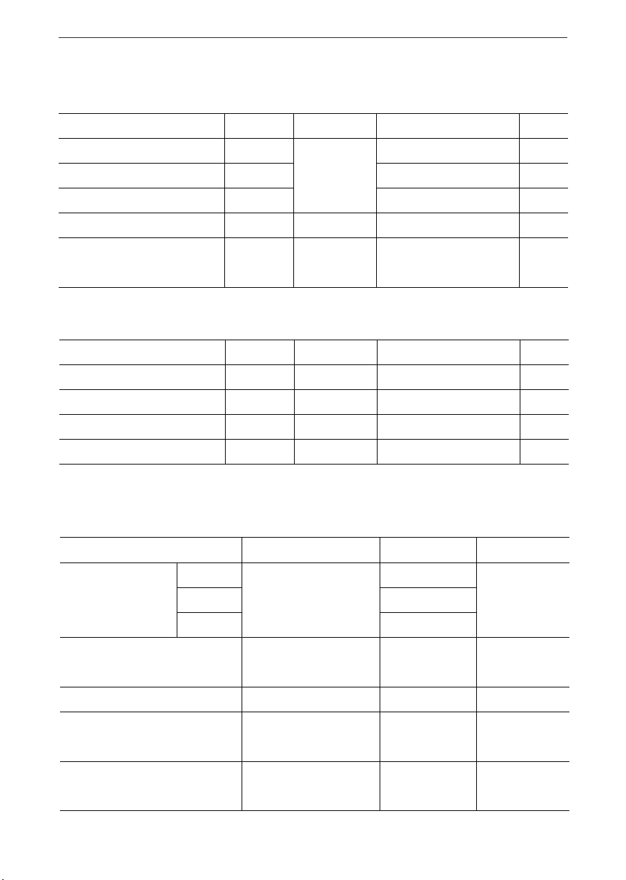
ELECTRICAL CHARACTERISTICS
Absolute Maximum Ratings
Parameter Symbol Conditions Rating Unit
Power supply voltage
Input voltage V
I
Output voltage Vo
Storage temperature
Soldering conditions (lead)
Operating Conditions
Parameter Symbol Conditions Rating Unit
Power supply voltage
Time Recording Supply Voltage
Crystal Frequency
Operating Temperature
Note:
Time Recording Supply Voltage: Power supply voltage to guarantee a crystal oscillator and time recording
Frequency Accuracy
Item Conditions Rating Unit
V
DD
Ta = 25°
T
STG
T
SOL
V
DD
V
CLK
f
(XT)
T
OP
—
—
—
—
—
—
– 0.3 to 7
-03 to VDD +0.3
-03 to VDD +0.3
–55 to +85
Temp.:under 260°C
Time :within 10 seconds
4.5 to 5.5
2.0 to 5.5
32.768
–40 to +85
V
V
V
°C
V
V
kHz
°C
Frequency stability
Temperature Characteristics
OCS starting time
Frequency Drift
Voltage characteristics
Rank A : 18pin DIP only
*
Rank S : 24pin SOP only
Rank B : 18pin DIP, 24pin SOP
Rank A
Rank S
Rank B
Ta = 25°C
VDD = 5V
–10 to +70°C (25°C standard)
–40 to +85°C (
´´
At 4.5V, let "t" make "0"
Ta=25°C, V
DD
= 5V
First year
Ta=25°C
V
= 4.5~5.5V
DD
± 10
± 20
PPM
± 50
+10/ –120
)
+10/ –220
MAX 1
± 5
± 5
PPM
Sec.
PPM/year
PPM/V
45
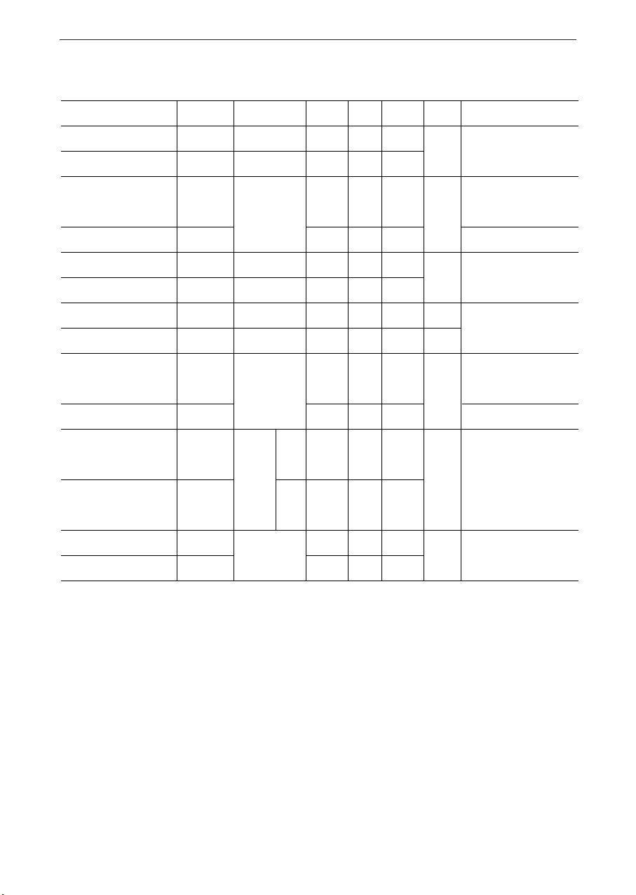
D.C. Characteristics
(V
DD
Parameter Symbol Conditions Applicable TerminalUnit
Min.
Typ.
¡ SemiconductorMSM62X42B
= 5V ± 10%, Ta = –40 to +85°C)
ax
"H" Input voltage (1)
"L" Input voltage (1)
Input leak current (1)
Input leak current (2)
"L" output voltage (1)
"H" output voltage
"L" output voltage (2)
OFF leak current
Input capacitance (1)
Input capacitance (2)
Current
consumption (1)
Current
consumption (2)
"H" input voltage (2)
"L" input voltage (2)
V
IH1
V
IL1
I
LK1
I
LK2
V
OL1
V
OH
V
OL2
I
OFFLK
C11
C12
I
DD1
I
DD2
V
1H2
V
1L2
V1 = VDD/0V
IOL = 2.5mA
IOH = 400µ A
IOL = 2.5mA
VI = VDD/0V
Input frequency 1MHz
f(xt) =
32.768
V
DD
= 5V
kHz
~
CS1
~
V
=2~5.5V
DD
DD
= 2V
0V
V
4/5V
2.2
—
—
—
—
2.4
—
—
—
—
—
—
—
—
—
—
0.8
—
1/–1
—
10/–10
—
0.4
—
—
—
0.4
All input terminals
V
except CS
Input terminals other
than D0 ~D
µA
D0 ~ D
V
D0 ~ D
V
1
3
3
3
STD. P
—
10
µA
5
—
5
—
—
30
—
1.8
—
DD
—
—
1/5V
DD
Input terminals other
than D
PF
D0 ~D
V
µA
DD
CS1
V
3
to D
0
3
46
¡ Semiconductor MSM62X42B
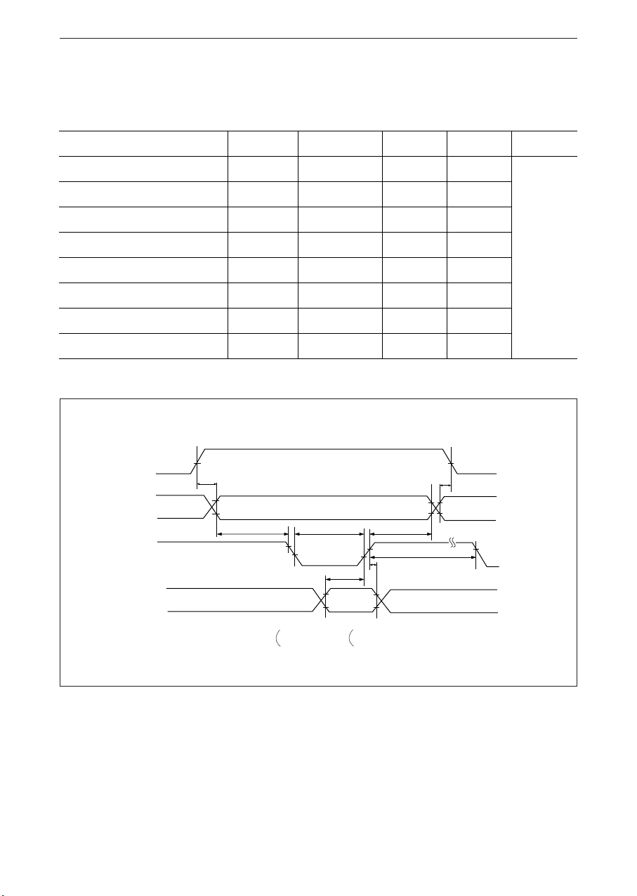
Switching Characteristics
WRITE mode (ALE = VDD)
(V
= 5V ± 10%, Ta = –40 to +85°C)
DD
Parameter Symbol Conditions Min. Unit
Max.
CS1 Set up Time
CS1 Hold Time
Address Stable Before WRITE
Address Stable After WRITE
WRITE Pulse Width
Data Set up Time
Data Hold Time
RD/WR Recovery Time
CS
1
A0~A
3
CS
0
WR
D0~D
3
(INPUT)
t
C1S
t
C1H
t
AW
t
WA
—
—
—
—
1000
1000
20
10
—
—
—
—
ns
t
WW
t
DS
t
DH
t
RCV
V
IH2
t
C1S
V
IH1
V
IL1
t
Aw
V
IH1
—
—
—
—
t
ww
V
V
IL1
t
DS
V
IH1VIH1
V
IL1VIL1
IL1
120
100
10
60
t
wA
V
IH1
t
RCV
t
DH
—
—
—
—
V
IH2
t
C1H
V
IH1
V
IL1
V
IH1
V
V
IH1
IL1
= 2.2V
= 0.8V
V
=
4
/5
V
IH2
V
DD
1
/5
V
=
DD
IL2
47
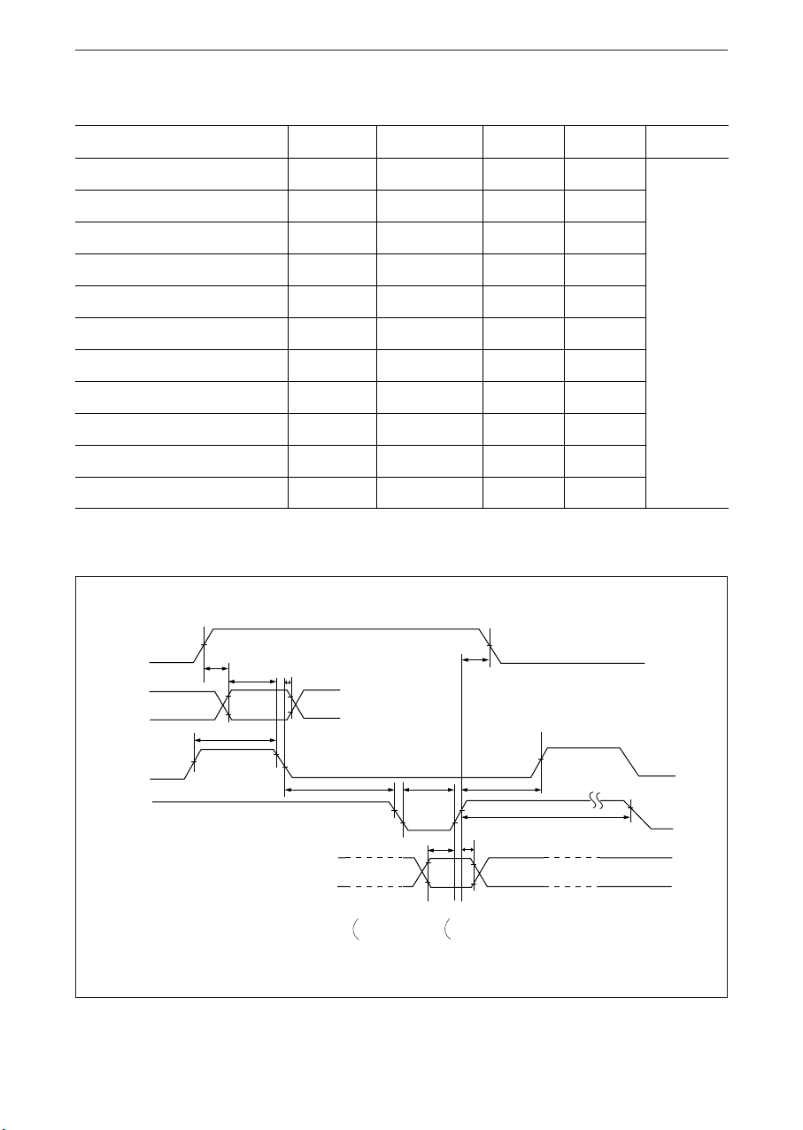
WRITE mode (with use of ALE)
Parameter Symbol Conditions Min. Unit
¡ SemiconductorMSM62X42B
(V
= 5V ± 10%, Ta = –40 to +80°C)
DD
Max.
CS1 Set up Time
Address Set up Time
Address Hold Time
ALE Pulse Width
ALE Before WRITE
WRITE Pulse Width
ALE After WRITE
Data Set up Time
Data Hold Time
CS1 Hold Time
RD/WR Recovery Time
CS
1
A0~A
3
CS
0
ALE
WR
D
0~D3
(Input)
t
C1S
t
AS
t
AH
t
AW
t
ALW
t
WW
t
WAL
t
DS
t
DH
t
C1H
t
RCV
V
IH2
t
C1S
t
t
AS
AH
V
IH1
V
IL1
t AW
V
V
IH1
V
IH1
V
IL1
IH1
V
IL1
t
ALW
V
—
—
—
—
—
—
—
—
—
—
—
t
WW
IH1
V
IL1
t
DS
V
IH1
V
IL1
1000
25
25
40
10
120
20
100
10
1000
60
V
IH2
t
C1H
t
WAL
V
IH1
V
IL1
t
t
RCV
DH
V
IH1
V
IL1
—
—
—
—
—
—
ns
—
—
—
—
—
V
IH1
48
V
V
IH1
IL1
= 2.2V
= 0.8V
V
=
4
/5
V
IH2
V
IL2
DD
1
/5
V
=
DD
¡ Semiconductor MSM62X42B
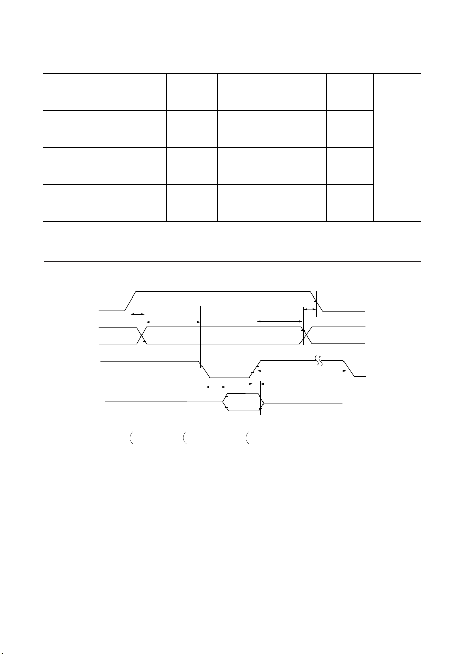
READ mode (ALE = VDD)
(V
= 5V ± 10%, Ta = –40 to +85°C)
DD
Parameter Symbol Conditions Min. Unit
Max.
CS1 Set up Time
CS1 Hold Time
Address Stable Before READ
Address Stable After READ
RD to Data
Data Hold
RD/WR Recovery Time
CS
1
A0~A
3
CS
0
RD
D0~D
3
(Output)
t
C1S
t
C1H
t
AR
t
RA
t
RD
t
DR
t
RCV
V
IH2
t
C1S
t
AR
V
IH1
V
IL1
V
IH1
V
t
IL1
RD
—
—
—
—
CL = 150 pF
—
—
V
IL1
V
OH
V
OH
V
V
OL
OL
1000
1000
20
0
—
0
60
t
C1H
t
RA
V
IH1
t
RCV
t
DR
—
—
—
ns
120
—
—
V
IH2
V
IH1
" Z "
V
V
IH1
IL1
= 2.2V
= 0.8V
V
=
4
/5
V
IH2
1
/5
V
=
V
IL2
VOH = 2.2V
DD
DD
V
= 0.8V
OL
49
 Loading...