OKI MSM6262-xxGS-BK Datasheet

E2B0033-27-Y2
¡ Semiconductor MSM6262-xx
¡ Semiconductor
This version: Nov. 1997
Previous version: Mar. 1996
MSM6262-xx
DOT MATRIX LCD CONTROLLER WITH 48-DOT COMMON DRIVER
GENERAL DESCRIPTION
The MSM6262-xx is a dot matrix LCD controller which is fabricated by OKI's low power
consumption CMOS silicon gate technology. In combination with 8-bit microcontroller, the
MSM6262-xx can control the dot matrix character type LCD module.
The MSM6262-xx is provided with a serial data transfer output. So, a maximum of 160 characters
can be controlled by combining this device with the MSM5259, MSM5839C, or MSM5260.
The MSM6262-xx is recommended for use in an LCD panel which is capable of displaying 81 to
160 characters. If an LCD panel of which display capacity is 80 characters or less is used, the
MSM6222B-xx is recommended.
The MSM6262-xx is best suited to be used as an LCD controller for applications such as electronic
typewriters, POS system terminals, and data banks.
FEATURES
• Dot matrix LCD controller/driver for three different font configuration
(5 x 7 dots, 5 x 11 dots and 5 x 12 dots)
• Up to 160 characters can be controlled
(Display data RAM ... 160 x 9-bit)
• On-chip character generator ROM (CGROM) for 256 different characters
5 x 7 dots ... 128 characters
5 x 11 dots ... 96 characters
5 x 12 dots ... 32 characters
• On-chip character generator RAM (CGRAM) (32 x 8-bit)
5 x 8 dots ... 4 kinds
5 x 12 dots ... 2 kinds
• Easy interface with Z80, 6809, 80C49, and 80C51
• Underline function
• Shift function for g, i, p, q and y
• Selectable driving duty
Duty Font Configuration (dots) Cursor Display Display (characters x lines)
1/16 5 x 7 80 x 2
1/24 5 x 11 80 x 2
1/32 5 x 7 40 x 4
1/48 5 x 11 40 x 4
Available
Available
Available
Available
• Package :
80-pin plastic QFP (QFP80-P-1420-0.80-BK) (Product name : MSM6262-xxGS-BK)
xx indicates code number.
1/52
¡ Semiconductor MSM6262-xx
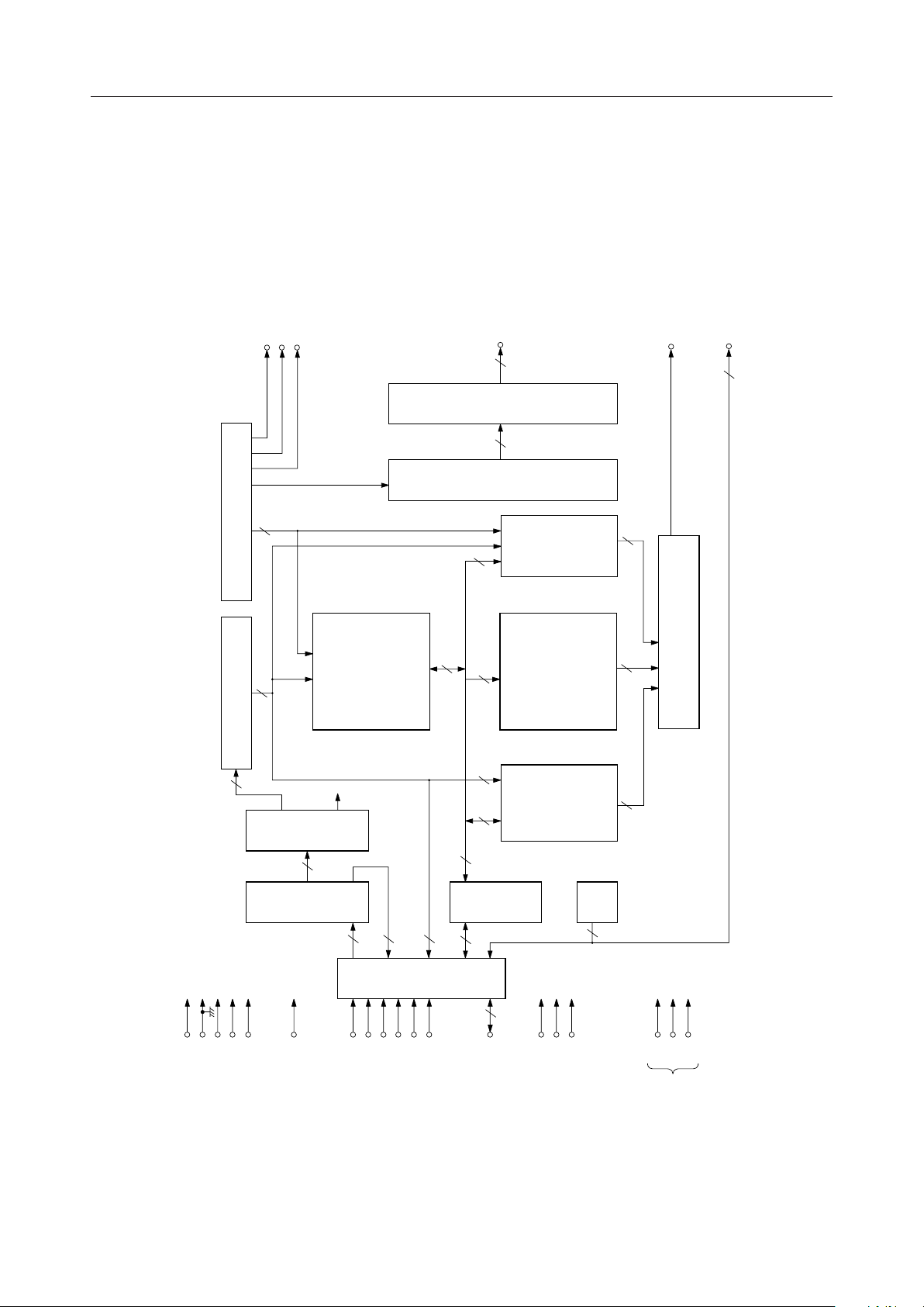
BLOCK DIAGRAM
CP
LOAD
DF
8
Timing generator
8
Address counter (ADC)
8
Display data RAM
(DDRAM)
160 x 9 bits
COM-
MON
48-bit
shift
9
signal
driver
register
1
8
5
COM1 - COM48
4848
Cursor
blink,
Character generator
under-line
function
control
ROM (CGROM),
11,680 bits
DO
BUSY1 OUT
BUSY2 OUT
2
1
5
Parallel / Serial converter
256 bits
Busy
flag
5
Instruc-
tion
9
Instruc-
tion
decoder
register
(I/R)
Character
generator
RAM
8
(CGRAM),
9
Data
register
(DR)
6
Input/
Output
buffer
8
8
9
2
8
A0
SS
DD
V
V
OSC1
OSC2
OSC3
RESET
CS
68 series/80 series
A1
E (RD)
R/W (WR)
7
- DB
0
DB
TEST1
TEST2
TEST3
1V4V5
V
LCD driving
voltage
2/52
¡ Semiconductor MSM6262-xx
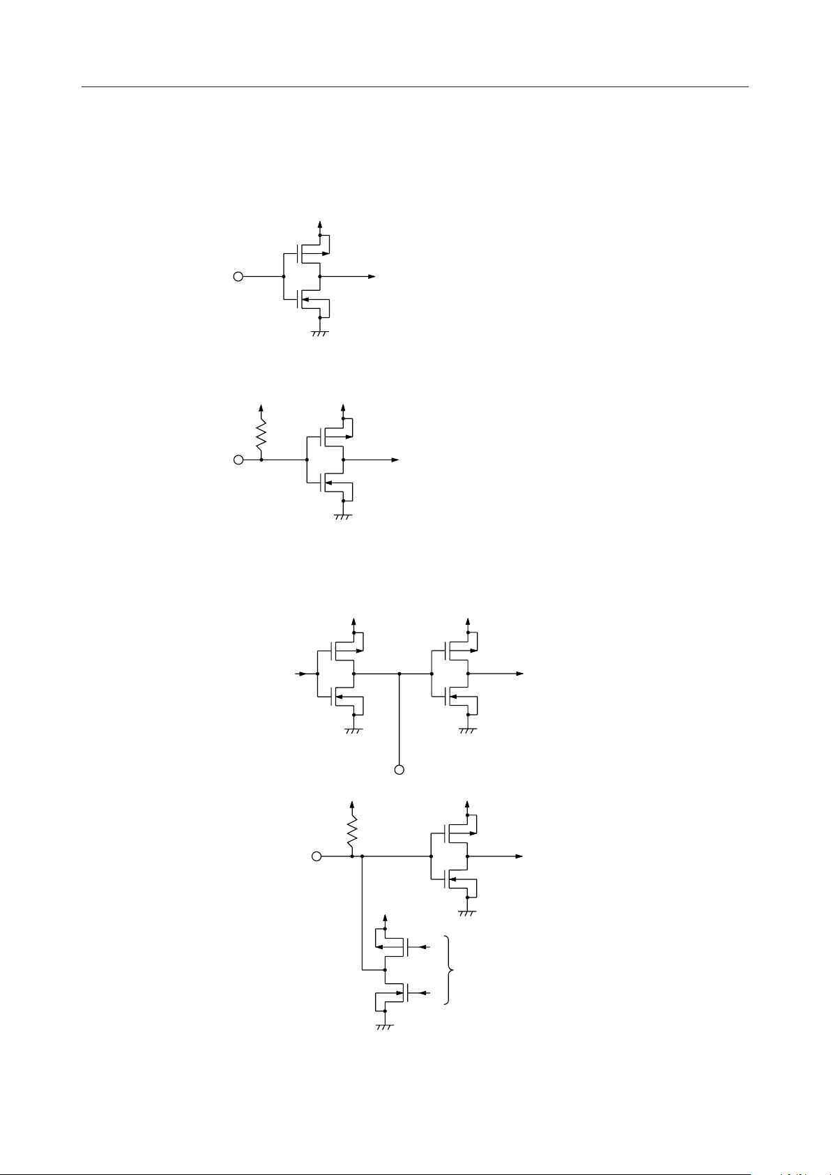
INPUT AND OUTPUT CONFIGURATION
Input pin
V
DD
To the inside of the device
V
DD
Input /Output pin
From the inside of the device
Applicable pins:
OSC1, 68 series/80 series, CS
R/W (WR), E (RD)
A0, A1
V
DD
To the inside of the device
V
DD
Applicable pin:
V
DD
RESET
To the inside of the device
Applicable pins:
V
DD
V
DD
OSC2, OSC3
To the inside of of the device
V
DD
From the inside of the device
Applicable pins: DB
- DB
0
7
3/52

¡ Semiconductor MSM6262-xx
Output pin
From the inside of the device
Applicable pins:
CP, LOAD, DF, DO,
BUSY1 OUT, BUSY2 OUT
4/52

¡ Semiconductor MSM6262-xx
PIN CONFIGURATION (TOP VIEW)
COM 45
COM 44
COM 43
COM 42
COM 41
COM 40
COM 39
COM 38
COM 37
COM 36
COM 35
COM 34
COM 33
COM 32
COM 31
COM 30
COM 46
COM 47
COM 48
(GND)
V
SS
OSC1
OSC2
OSC3
TEST1
TEST2
TEST3
RESET
68 series/80 series
CS
E (RD)
R/W (WR)
A0
A1
DB
DB
DB
DB
DB
DB
DB
807978777675747372717069686766
1
2
3
4
5
6
7
8
9
10
11
12
13
14
15
16
17
18
0
19
1
20
2
21
3
22
4
23
5
24
6
252627282930313233343536373839
7
DB
DF
LOAD
CP
DO
DD
V
V1V4V
5
COM 1
COM 2
COM 3
COM 4
65
64
63
62
61
60
59
58
57
56
55
54
53
52
51
50
49
48
47
46
45
44
43
42
41
40
COM 5
COM 29
COM 28
COM 27
COM 26
COM 25
COM 24
COM 23
COM 22
COM 21
COM 20
COM 19
COM 18
COM 17
COM 16
COM 15
COM 14
COM 13
COM 12
COM 11
COM 10
COM 9
COM 8
COM 7
COM 6
BUSY 1 OUT
BUSY 2 OUT
80-Pin Plastic QFP
5/52

¡ Semiconductor MSM6262-xx
PIN DESCRIPTIONS
Symbol Type
OSC1
OSC2, OSC3
RESET
68 series/80 series
CS
R/W (WR)
E (RD)
A0, A1
DB
- DB
0
7
TEST1 - TEST3
V
, V
DD
SS
V1, V
4, V5
DO
CP
LOAD
DF
COM1 - COM48
BUSY1 OUT
BUSY2 OUT
I/O
I/O
—
—
O
O
O
O
O
O
O
Description
Clock oscillating pins required for internal operation upon receipt
of the LCD drive signal and CPU instruction.
I
I
I
Reset pin
Selection pin for either 68 series CPU or 80 series CPU
Chip select pin. By setting CS at "L" level, MSM6262-xx
is set at selecting condition.
I
R/W pin of 68 series CPU shall be connected to this pin,
while WR pin shall be connected to this pin in the case of
80 series CPU.
I
E pin of 68 series CPU shall be connected to this pin,
while RD pin shall be connected to this pin in the case of
80 series CPU.
I
The address bus of CPU shall be connected to these pins.
Instruction code is set by these pins.
The data bus of CPU shall be connected to these pins. These
pins are used to set the data of the instruction or to read
the data.
I
Test pins. Normally these pins should be set at V
SS
or
open.
Voltage supply pins. V
is also used for the common
DD
bias voltage level to drive the LCD.
Common bias voltage input pins to drive the LCD
Serial data output pin for SEGMENT drivers
Clock pulse output pin. The clock output from this pin
enables the character pattern data, which is output from
DO, to input to the SEGMENT drivers (MSM5839C or MSM5259).
Load signal output pin. The character pattern data to
the SEGMENT drivers, which was output from DO and
CP, is loaded to the LCD output of the SEGMENT
drivers, synchronized with the COMMON signal.
B-type AC signal output pin to drive the LCD
COMMON signal output pins to drive the LCD
This pin shows the internal condition of MSM6262-xx.
"H" shows that MSM6262-xx is in internal operation,
while "L" shows that MSM6262-xx is ready to receive
the instruction from the CPU.
This pin shows that MSM6262-xx is in internal operation
based on the instruction from the CPU, or MSM6262-xx
is in display revising operation based on the instruction
from the CPU.
"H" shows that MSM6262-xx is in internal operation,
while "L" shows that the display on the LCD has been
established and the MSM6262-xx is ready to receive an
instruction.
6/52
¡ Semiconductor MSM6262-xx
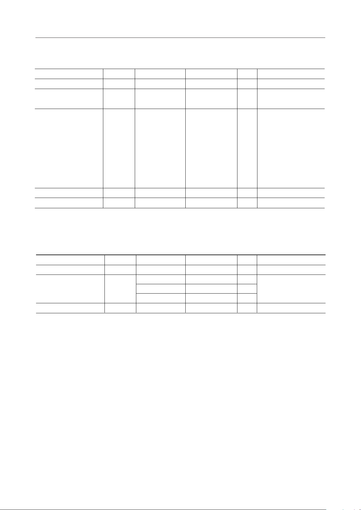
ABSOLUTE MAXIMUM RATINGS
Parameter Symbol Condition Rating Unit
Supply Voltage V
Supply Voltage
, V4, V
V
for Driving LCD
1
Input Voltage V
Power Dissipation
Storage Temperature
T
P
STG
Ta = 25°C, VDD–V
DD
5
IN
D
SS
Ta = 25°C
VDD – 12 to
V
DD
+ 0.3
Ta = 25°C –0.3 to VDD + 0.3 V
Ta = 25°C
––
500 mW
–55 to +125
RECOMMENDED OPERATING CONDITOINS
Applicable Pin
V–0.3 to +7.0 V
VV
DD, VSS
, V4, V
1
5
OSC1, RESET
68 series / 80 series
CS, A0, A1, R/W (WR)
E (RD), DB
- DB
0
––
°C
––
7
Parameter Symbol Condition Range Unit
Supply Voltage V
LCD Driving Voltage
Operating Temperature
DD
V
T
LCD
op
1/6, 1/7 bias, VDD–V
––
1/5 bias, VDD–V
1/8 bias, V
DD–V5
––
5
3.0 to 11
4.0 to 11
5
4.5 to 11
–20 to +75
Note: For bias, refer to *3 in the section "DC Characteristics".
Applicable Pin
V4.5 to 5.5 V
V
V
V
V
°C
DD,
DD, V1
GND
, V4, V
––
5
7/52
¡ Semiconductor MSM6262-xx
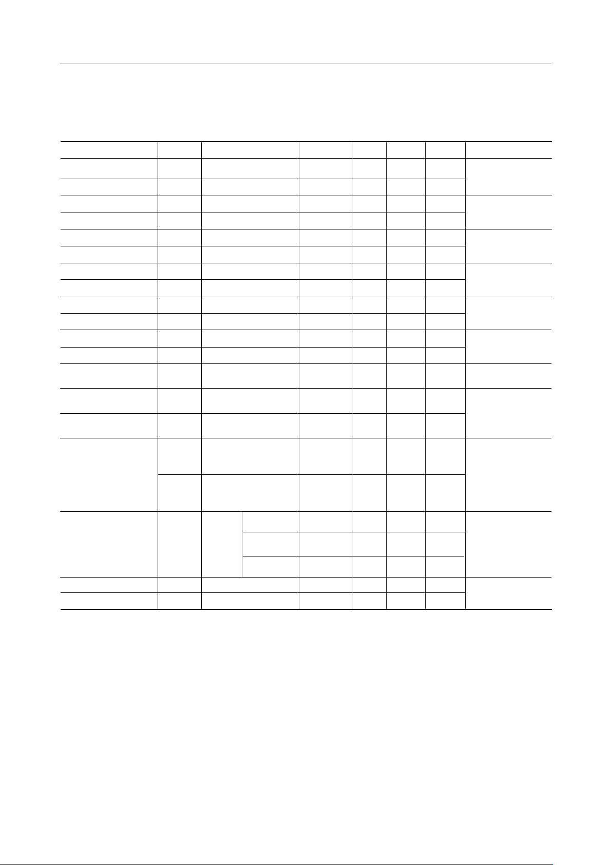
ELECTRICAL CHARACTERISTICS
DC Characteristics
(V
DD
Parameter Symbol Condition Min. Typ. Max. Unit
"H" Input Voltage
"L" Input Voltage
"H" Output Voltage
"L" Output Voltage
"H" Input Voltage
"L" Input Voltage
"H" Output Voltage
"L" Output Voltage
"H" Output Voltage
"L" Output Voltage
"H" Output Voltage
"L" Output Voltage
COM Voltage Drop
"H" Input Current
"L" Input Current
V
V
V
V
V
V
V
V
V
V
V
V
V
I
I
I
DD1
IH1
IL1
OH1
OL1
IH2
IL2
OH2
OL2
OH3
OL3
OH4
OL4
COM
ILH1
ILL1
––
––
I
= –250 mA
O
I
= 1.8 mA
O
––
––
I
= –500 mA
O
I
= 500 mA
O
I
= –1 mA
O
I
= 1 mA
O
= –100 mA
I
O
I
= 1.6 mA
O
IO = ± 50 mA COM1 - COM48
V
= V
IN
DD
VIN = V
SS
*2
= 5 V,
V
DD
f
= 500 kHz
OSC
*1
2.2
–0.3
2.4
––
–0.8
V
DD
–0.3
0.85 V
––
0.85 V
––
2.4
––
––
––
––
––
DD
DD
––
––
––
––
––
––
––
––
––
––
––
––
––
––
––
––
V
DD
0.7
––
0.4
V
DD
0.8
––
0.15 V
––
0.15 V
––
0.4
2.9
–1
1.5
(RC oscillation)
Supply Current
I
DD2
*2
V
= 5 V,
DD
fIN = 500 kHz
––
––
1.5
(external oscillation)
= 4.5 to 5.5 V , Ta = –20 to +75°C)
Applicable Pin
V
V
V
CS, R/W (WR)
E (RD), A0, A1
DB0 - DB
DB0 - DB
7
7
V
DD
DD
V
V
V
V
V
V
V
V
OSC1, RESET
68series/80series
DO, LOAD, DF
CP
BUSY1 OUT
BUSY2 OUT
V
1
mA
mA
CS, R/W (WR)
E (RD), A0, A1
OSC1, 68series/
80series
mA
V
DD
mA
11
11
11
–60
V
V
V1 , V4, V
5
V
2
mA
mA
RESET
and COM1
5
LCD Driving
Voltage
"H" Input Current
"L" Input Current
V
I
ILH2
I
ILL2
LCD
1/5 bias
*3
V
DD–V5
1/6-1/7
bias
1/8 bias
V
= V
IN
DD
VIN = VSS,VDD = 5 V
3.0
4.0
4.5
––
–8
––
––
––
––
–20
*1. This is applicable to the voltage drop which is caused between VDD, V1, V4, V
- COM48 when a current of 50 mA is flowed in/out to/from all of COM1 - COM48. (When
the output level is either VDD or V1, it should be applied only when the current flows in.
When the output level is either V4 or V5, it should be applied only when the current flows
in.
In this case, +5V is applied to VDD and V1, while –6 V is applied to V4 and V5.)
*2. This is applicable to the current which flows in to VDD under following conditions.
VDD = 5 V, VSS = 0 V, V1 = 2.8 V, V4 = -3.8 V, V5 = –6 V, No load, No interface with CPU
*3. V1 to V5 should be set at as follows.
8/52
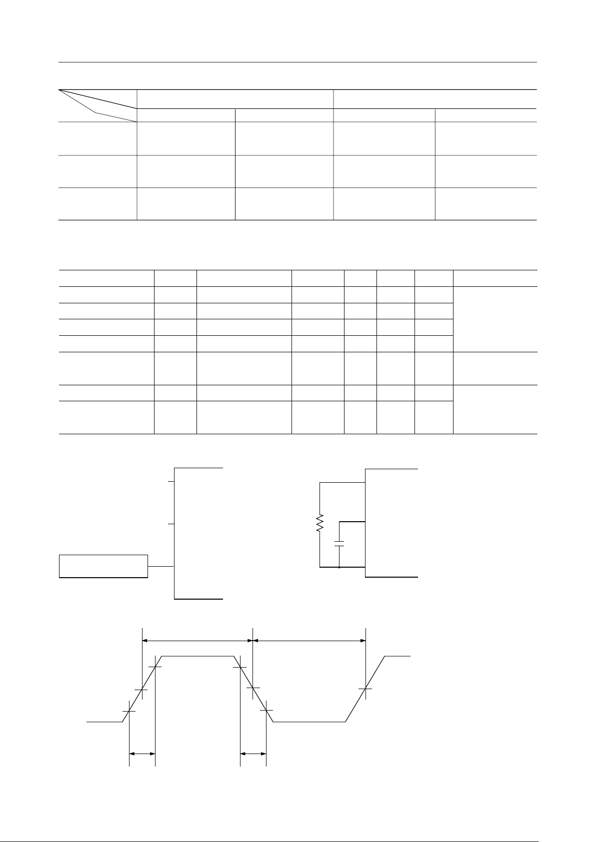
¡ Semiconductor MSM6262-xx
No. of lines
(N)
Font
configuration
Pin
V
1
V
4
V
5
= LCD driving voltage
V
LCD
AC Characteristics
5 x 8 5 x 12 5 x 8 5 x 12
1
VDD – –– V
5
4
VDD – –– V
5
VDD – V
2 lines 4 lines
1
V
– –– V
DD
7
6
VDD – –– V
7
VDD – V
(V
LCD
DD
LCD
LCD
LCD
1
V
– –– V
DD
6
5
VDD – –– V
6
VDD – V
LCD
LCD
LCD
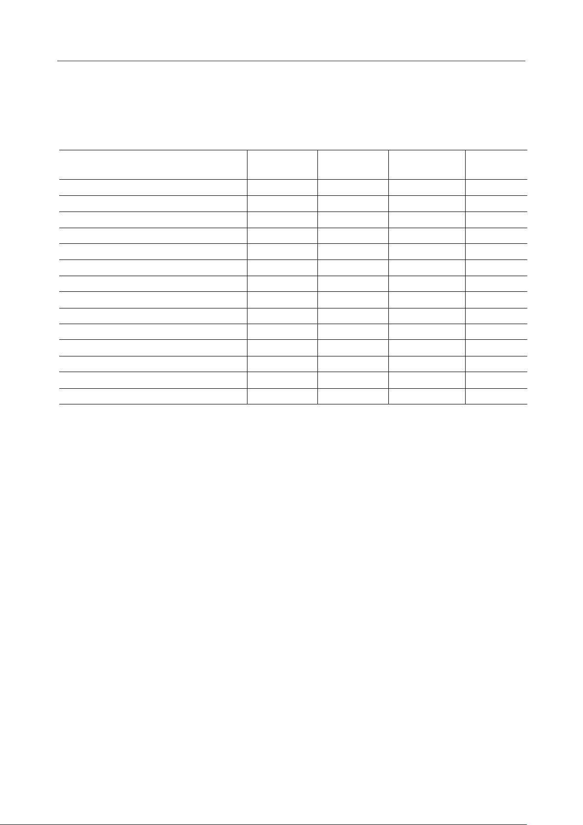
Parameter Symbol Condition Min. Typ. Max. Unit
Input Frequency
Input Clock Duty
Input Clock Rise Time
Input Clock Fall Time
RC Oscillation
Frequency
"H" Input Current
"L" Input Current
f
f
DUTY
f
I
ILH3
I
ILL3
IN
t
t
CR
*1, *2
*2
r
f
*2
*2
*3
VIN = V
DD
V
= V
IN
SS
300
45
––
––
300
––
–45
500
50
––
––
500
––
–120
700
55
100
100
700
–250
VDD = 5 V
1
V
LCD
LCD
– –– V
DD
8
7
VDD – –– V
8
VDD – V
LCD
LCD
LCD
= 4.5 to 5.5V , Ta = –20 to +75°C)
Applicable Pin
kHz
%
OSC1
ns
ns
OSC1, OSC2, OSC3
kHz
1
mA
DB
- DB
0
7
mA
*1
Oscillation source
*2
VDD–0.8 V
0.5 V
DD
0.8 V
Open
Open
t
r
OSC3
OSC2
OSC1
T
H
VDD–0.8 V
0.5 V
0.8 V
t
f
DD
R
*3
OSC3
= 39 kW ± 5%
R
f
OSC2
C
f
f
= 22 pF ± 10%
C
f
(Keep the wiring from
OSC1, OSC2, and
OSC1
OSC3 to R
and C
f
f
as short as possible.)
T
L
0.5 V
DD
T
H
= ––––––– x 100%
f
DUTY
TH + T
L
9/52
¡ Semiconductor MSM6262-xx
TIMING DIAGRAM
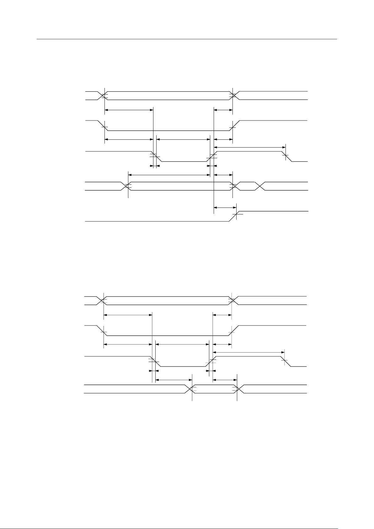
Interface with 80 Series CPU
(VDD = 4.5 to 5.5V, Ta = –20 to +75°C)
Parameter Symbol Min. Max. Unit
Address Set-up Time
CS Set-up Time
WR "L" Pulse Width
RD "L" Pulse Width
WR, RD "H" Pulse Width
Address Hold Time
CS Hold Time
Data Set-up Time
Data Hold Time (Write operation)
WR, RD Fall Time
WR, RD Rise Time
Data Delay Time
Data Hold Time (Read operation)
Busy Output Delay Time
t
SA1
t
SA2
t
WWR
t
WRD
t
WH
t
HA1
t
HA2
t
SWD
t
HWD
t
f
t
r
t
SRD
t
HRD
t
BD
110
100
320
320
210
25
25
300
20
––
––
––
––
––
––
––
––
––
––
––
––
––
25
25
190
0
––
410
ns
ns
ns
ns
ns
ns
ns
ns
ns
ns
ns
ns
ns
ns
10/52
¡ Semiconductor MSM6262-xx
Write operation
A0,A1
CS
V
IL
R/W (WR)
DB0 - DB7
BUSY 1 OUT, BUSY 2 OUT
Read operation
V
IH
V
IL
t
SA1
t
SWD
t
W WR
Valid data
t
r
t
SA2
V
IH
V
IL
t
f
V
IH
V
IL
t
t
V
V
t
HWD
V
V
HA1
HA2
IH
IL
V
V
t
BD
IH
IL
V
IL
t
WH
V
IH
IH
IL
V
OH
A0,A1
CS
E (RD)
DB0 - DB7
V
IH
V
IL
t
SA1
V
IL
t
SRD
t
WRD
V
OH
V
OL
t
SA2
V
IH
V
IL
t
f
Refer to the DC Characteristics for the definition of VIH, VIL, V
and VOL.
t
t
V
V
t
t
Valid data
V
IH
V
IL
HA1
HA2
IH
IL
r
HRD
OH
V
IL
t
WH
V
IH
V
OH
V
OL
11/52

¡ Semiconductor MSM6262-xx
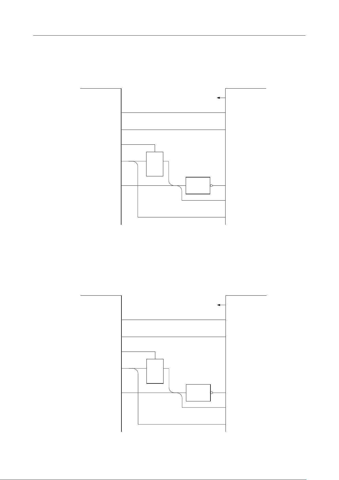
• Interface with Z80
Z80 MSM6262-xx
V
SS
A
WR
IORQ
- A
0
RD
15
*
*
*
Address
Decoder
*
*
- DB
DB
0
7
* A pull-up resistor of about 50 kW is required when the output of CPU becomes high impedance.
68 series/80 series
E (RD)
R/W (WR)
CS
A0, A1
DB0 - DB
7
12/52
¡ Semiconductor MSM6262-xx
• Interface with 80C49
MSM80C49 MSM6262-xx
RD
WR
V
SS
*
*
68 series/80 series
E (RD)
R/W (WR)
ALE
- DB
DB
0
7
STB
8282
P20
- P22
* A pull-up resistor of about 50 kW is required when the output of CPU becomes high impedance.
Address
Decoder
*
*
CS
A0, A1
DB0 - DB
7
• Interface with 80C51
MSM80C51 MSM6262-xx
- P07
P00
- P22
P20
* A pull-up resistor of about 50 kW is required when the output of CPU becomes high impedance.
RD
WR
ALE
*
*
8282
STB
V
Address
Decoder
SS
68 series/80 series
E (RD)
R/W (WR)
CS
*
A0, A1
*
- DB
DB
0
7
13/52
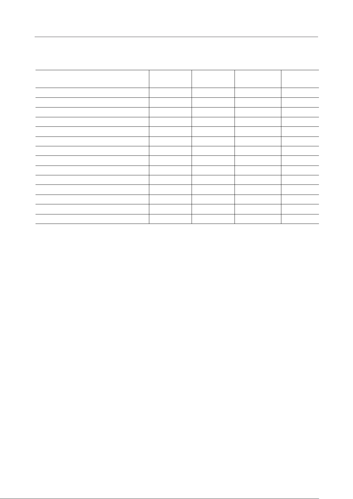
¡ Semiconductor MSM6262-xx
Interface with 68 Series CPU
(VDD = 4.5 to 5.5 V, Ta = –20 to +75°C)
Parameter Symbol Min. Max. Unit
Cycle Time
Address, R/W Set-up Time
CS Set-up Time
E signal "H" Pulse Width
E signal "L" Pulse Width
Address, R/W Hold Time
CS Hold Time
Data Set-up Time
Data Hold Time (Write operation)
E signal Rise Time
E signal Fall Time
Data Delay Time
Data Hold Time (Read operation)
Busy Output Delay Time
t
C
t
B1
t
B2
t
W
t
L
t
A1
t
A2
t
I
t
H
t
r
t
f
t
D
t
O
t
BD
500
100
90
220
210
20
20
225
30
––
––
––
10
––
––
––
––
––
––
––
––
––
––
25
25
180
––
410
ns
ns
ns
ns
ns
ns
ns
ns
ns
ns
ns
ns
ns
ns
14/52
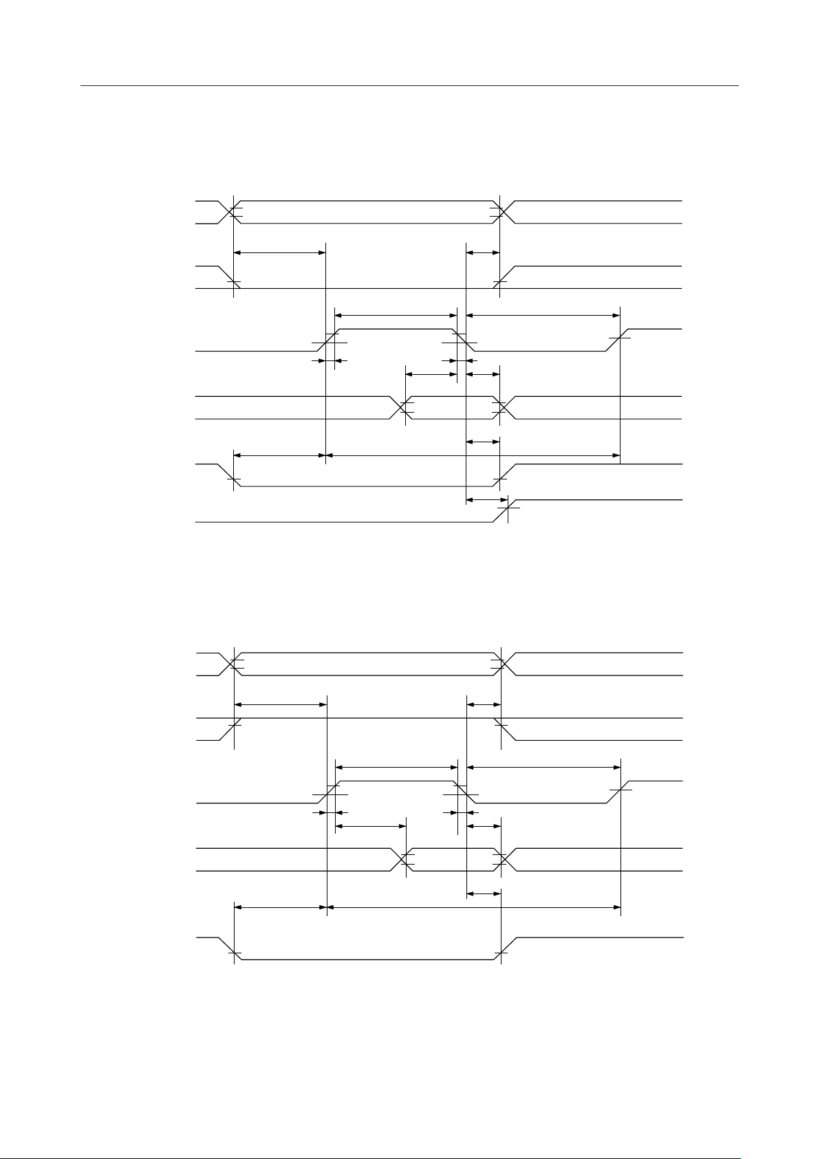
¡ Semiconductor MSM6262-xx
Write operation
A0, A1
R/W (WR)
E (RD)
DB0 - DB7
CS
Busy 1 OUT, Busy 2 OUT
Read operation
V
IH
V
IL
t
B1
V
IL
t
W
V
IH
V
IL
t
r
V
IH
V
IL
t
B2
V
IL
t
C
t
I
t
f
Valid data
V
IH
V
IL
t
A1
V
IL
t
L
V
IH
V
IL
t
H
V
IH
V
IL
t
A2
V
IL
t
BD
V
OH
V
IL
A0, A1
R/W (WR)
E (RD)
DB0 - DB7
CS
V
IH
V
IL
t
B1
V
IH
t
W
V
IH
V
IL
t
r
t
B2
V
IL
t
D
V
OH
V
OL
t
C
t
f
Valid data
V
IH
V
IL
t
A1
V
V
IH
V
IL
t
O
t
A2
V
Refer to the DC Characteristics for the definition of VIH, VIL, VOH, and VOL.
IH
t
L
V
IL
V
OH
V
OL
IL
15/52

¡ Semiconductor MSM6262-xx
• Interface with 6809
6809 MSM6262-xx
V
O
E
R/W
- A
A
0
15
Address
decoder
DD
*
*
*
*
- DB
DB
0
7
* A pull-up resistor of about 50 kW is required when the output of CPU becomes high impedance.
68 series/80 series
E (RD)
R/W(WR)
CS
A0, A1
DB0 - DB
7
16/52
 Loading...