OKI MSM6242B Datasheet

¡ Semiconductor MSM6242B
¡ Semiconductor
MSM6242B
DIRECT BUS CONNECTED CMOS REAL TIME CLOCK/CALENDAR
DESCRIPTION
The MSM6242B is a silicon gate CMOS Real
Time Clock/Calendar for use in direct busconnection Microprocessor/Microcomputer
applications. An on-chip 32.768 KHz crystal
oscillator time base is divided to provide addressable 4-bit I/O data for SECONDS,
MINUTES, HOURS, DAY OF WEEK, DATE,
MONTH and YEAR. Data access is controlled
by 4-bit address, chip selects (CSO, CS1),
WRITE, READ, and ALE. Control Registers
D, E and F provide for 30 SECOND error
adjustment, INTERRUPT REQUEST (IRQ
FLAG) and BUSY status bits, clock STOP,
HOLD, and RESET FLAG bits, 4 selectable
INTERRUPTS rates are available at the STD.P
(STANDARD PULSE) output utilizing Control Register inputs T0, T1 and the ITRPT/
STND (INTERRUPT/STANDARD). Masking of the interrupt output (STD.P) can be
accomplished via the MASK bit. The
MSM6242B can operate in a 12/24 hour format and Leap Year timing is automatic.
The MSM6242B normally operates from a 5V
±10% supply at –40 to 85°C. Battery backup
operation down to 2.0V allows continuation
of time keeping when main power is off. The
MSM6242B is offered in a 18-pin plastic DIP
and a 24-pin plastic Small Outline package.
FEATURES
DIRECT MICROPROCESSOR/MICROCONTROLLER BUS CONNECTION
TIME MONTH DATE YEAR DAY OF WEEK
23:59:59 12 31 80 7
• 4-bit data bus
• 4-bit address bus
• READ, WRITE, ALE and CHIP SELECT
INPUTS
• Status registers – IRQ and BUSY
• Selectable interrupt outputs – 1/64
second, 1 second, 1 minute, 1 hour
• Interrupt masking
• 32.768 KHz crystal controlled operation
• 12/24 hour format
• Auto leap year
• ±30 second error correction
• Single 5V supply
• Battery backup down to VDD = 2.0V
• Low power dissipation:
20µW max at V
150µW max at V
• 18 pin Plastic DIP (DIP18-P-300)
• 24 Pin-V Plastic SOP (SOP24-P-430-VK)
DD
DD
= 2V
= 5V
23
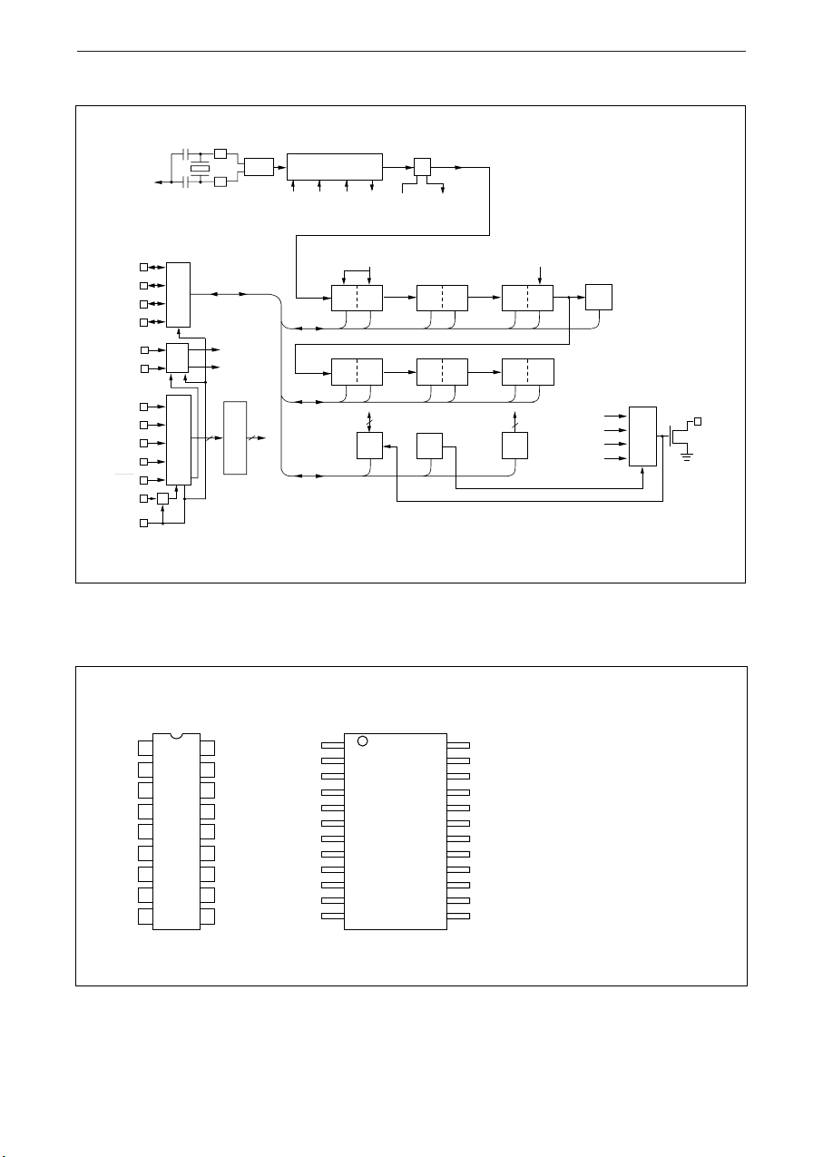
FUNCTIONAL BLOCK DIAGRAM
¡ SemiconductorMSM6242B
XT
32.768KHz
D
3
D
2
D
1
D
0
GATE
OSC
XT
WR
3
2
1
0
0
GATE
DECODER
GATE & LATCH
RD
A
A
A
A
CS
ALE
CS
1
PIN CONFIGURATION
COUNTER
30
STOP
RESET
bit
S
1
S
C
F
•
S
~W~Y10 are time counter register
1
C
•
0~CF
ADJ HOLD
bit
bit
30 sec
ADJ bit
S
S
10
1
D
D
10
1
C
D
are control register
1 Hz
BUSY
bit
bit
24/12bit
MI
MO
H
MI
1
10
MO
1
10
H
1
Y
Y
1
64Hz
W
10
10
STDP
1-sec carry
C
E
C
F
1-min carry
1-hour carry
STD.P
24
1
CS
2
0
3
ALE
4
A
0
5
A
1
A
6
2
A
7
3
8
RD
9
GND
18 pin Plastic DIP
STD.P
V
18
DD
17
XT
16
XT
15
CS
14
D
13
D
D
12
11
D
10
WR
CS
NC
ALE
1
0
1
2
3
NC
NC
RD
GND
1
2
0
3
4
5
A
0
6
A
7
1
8
A
9
2
A
10
3
11
12
24
23
22
21
20
19
18
17
16
15
14
13
V
XT
XT
NC
CS
D
NC
NC
D
D
D
WR
A
0-A3
DD
D
0-D3
CS
RD:
WR:
1
ALE:
0
STD.P:
XT, XT:
V
DD:
1
V
SS:
2
3
Data input/output
:
CHIP SELECTS 0,1
, CS1:
O
READ enable
WRITE enable
Address latch enable
Standard pulse output
XTAL oscillator input/output
+5V supply
ground
Address input
:
24 pin Plastic Small Outline
Package
¡ Semiconductor MSM6242B
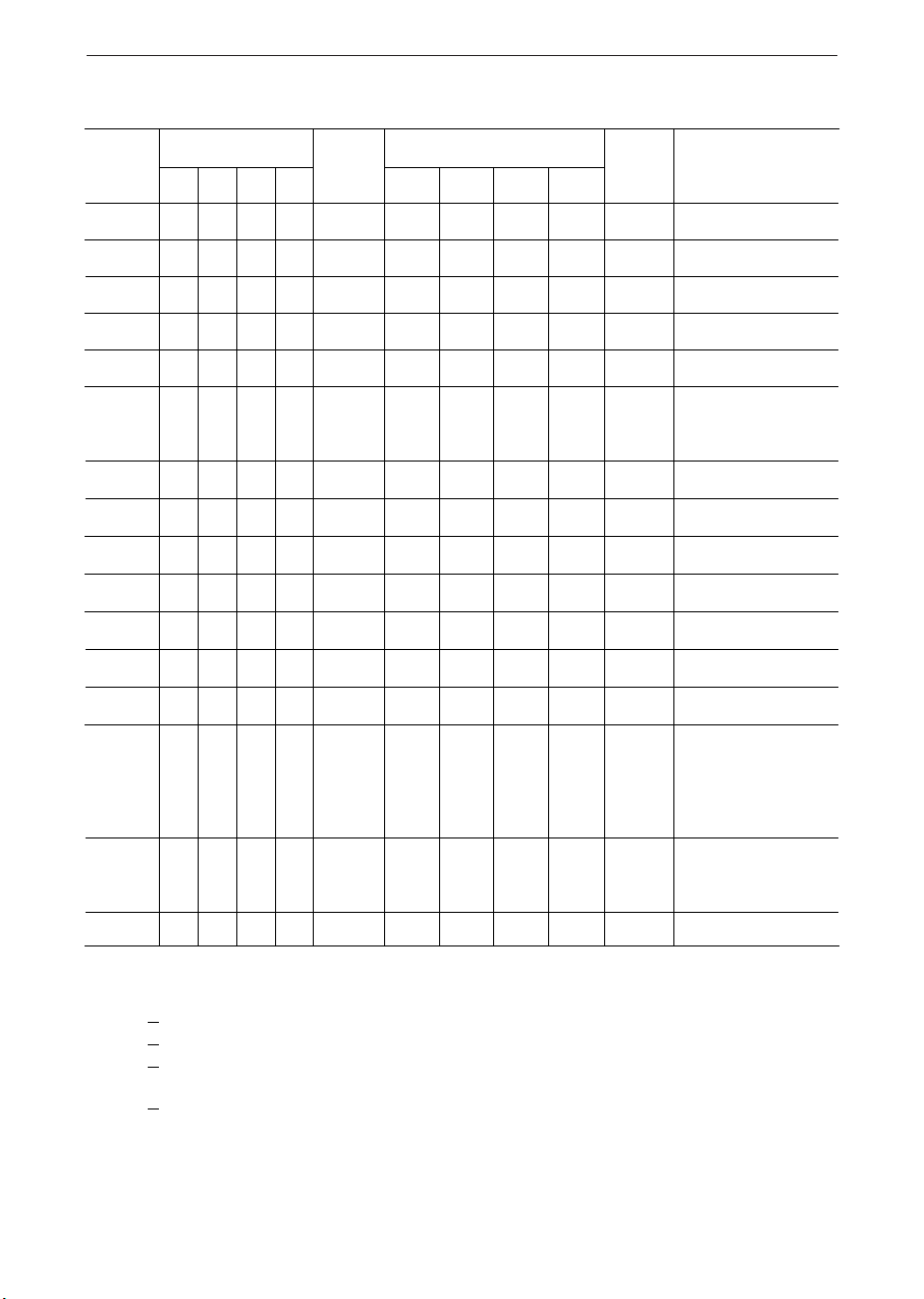
REGISTER TABLE
Address
Input
0
1
2
3
4
5
6
7
8
9
A
B
C
Address Input
A
A
3
0
0
0
0
0
0
0
0
1
1
1
1
1
A1A
2
0
0
0
0
0
1
0
1
1
0
1
0
1
1
1
1
0
0
0
0
0
1
0
1
1
0
0
0
1
0
1
0
1
0
1
0
1
0
1
0
Register
Name
S
1
S
10
MI
1
MI
10
H
1
H
10
D
1
D
10
MO
1
MO
10
Y
1
Y
10
W
D
mi
mo
y
Data
D
S
S
mi
mi
h
PM/
AM
d
mo
y
y
w
D
2
1
S
2
4
S
20
40
mi
2
4
mi
20
40
h
2
4
h
20
d
2
4
d
*
20
mo
2
4
*
*
y
2
4
y
20
40
w
2
4
3
S
8
*
8
*
h
8
*
d
8
*
8
*
y
8
80
*
D
S
mi
mi
h
d
mo
MO
y
Count
value
0
S
0 to 9
1
0 to 5
10
0 to 9
1
0 to 5
10
h
0 to 9
1
0 to 2
10
or 0 to 1
d
0 to 9
1
0 to 3
10
0 to 9
1
0 to 1
10
y
0 to 9
1
0 to 9
10
w
0 to 6
1
Description
1-second digit register
10-second digit register
1-minute digit register
10-minute digit register
1-hour digit register
PM/AM, 10-hour digit
register
1-day digit register
10-day digit register
1-month digit register
10-month digit register
1-year digit register
10-year digit register
Week register
1
1
0
D
1
E
F
1
1
1
1
1
0
1
1
REST = RESET
ITRPT/STND = INTERRUPT/STANDARD
Note 1)
Note 2)
Note 3)
Bit * does not exist (unrecognized during a write and held at "0" during a read).
Be sure to mask the AM/PM bit when processing 10's of hour's data.
BUSY bit is read only. The IRQ FLAG bit can only be set to a "0". Setting the IRQ FLAG to a "1" is done by
hardware.
Note 4)
PM at 1 and AM at 0 for PM / AM bit.
30
sec.
ADJ
t
1
TEST
IRQ
FLAG
t
0
24/12
C
D
C
E
C
F
Figure 1. Register Table
BUSY
ITRPT
/STND
STOP
HOLD
MASK
REST
—
—
—
Control Register D
Control Register E
Control Register F
25
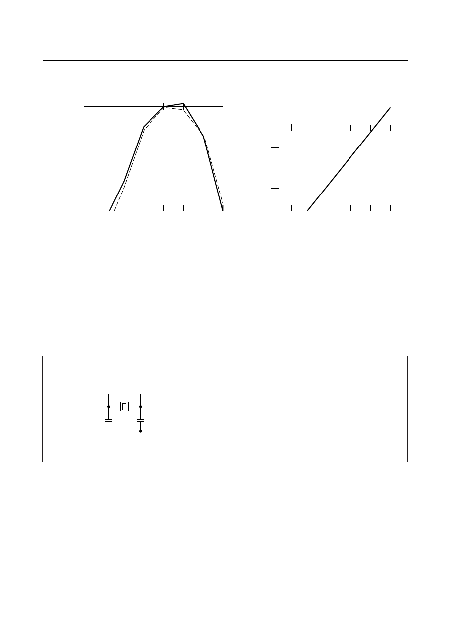
OSCILLATOR FREQUENCY DEVIATIONS
¡ SemiconductorMSM6242B
0
1
Ta = 25°C
0
-1
-50
∆f/f (PPM)
5V
-2
∆f/f (PPM)
-3
2V
-100
20 40 60 80
-60
-40 -20
0
Ta (°C)
Figure 2. Frequency Deviation (PPM) vs Temperature Figure 3. Frequency Deviation (PPM) vs Voltage
Note:
1. The graghs above showing frequency deviation vs temperature/voltage are primarily characteristic of the
-4
0
123456
V
(V)
DD
MSM6242B with the oscillation circuit described below.
XT
XT
Crystal: Type N0, P3 by kinseki (32.768 KHz)
C
G
C
D
V
DD
CG, CD: 22pF (Temperature Characteristics: 0)
26
¡ Semiconductor MSM6242B
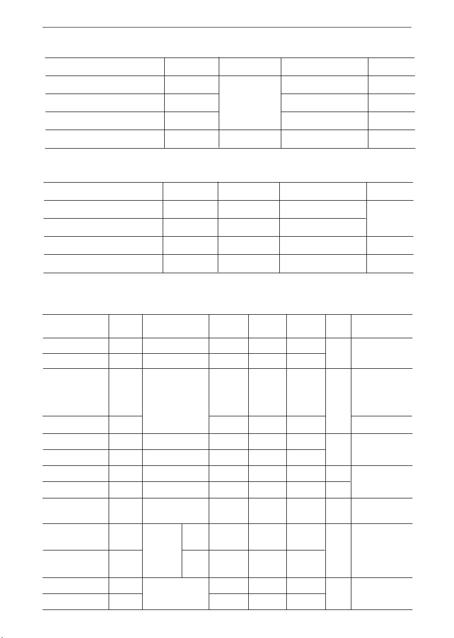
ABSOLUTE MAXIMUM RATINGS
Parameter Symbol Condition Rating
Power Supply Voltage
Input Voltage
Output Voltage
Storage Temperature
OPERATING CONDITIONS
Parameter Symbol Condition Rating
Power Supply Voltage
Standby Supply Voltage
Crystal Frequency
Operating Temperature
D.C. Characteristics
Parameter
"H" Input Voltage
"L" Input Voltage
Symbol
VIH1
VIL1
Condition
Unit
V
DD
V
I
V
O
T
STG
Ta = 25°C
-0. 3 to 7
-0.3 to VDD +0.3
-0.3 to VDD +0.3
-55 to +150
V
V
V
°C
Unit
V
DD
—
4 to 6
V
V
f
T
BAK
(XT)
OP
—
—
—
2 to 6
32.768
-40 to +85
kHz
°C
(VDD = 5V ± 10%, TA = -40 ~ +85)
Min.
—
—
2.2
—
Typ.
—
—
Max.
—
0.8
Unit
Applicable
All input termin-
V
als except CS1, XT
Terminal
Input Leak Current
Input Leak Current
"L" Output Voltage
"H" Output Voltage
"L" Output Voltage
OFF Leak Current
Input Capacitance
Current Consumption
Current Consumption
"H" Input Voltage
"L" Input Voltage
ILK1
ILK2
VOL1
V
VOL2
I
OFFLK
C
IDD1
IDD2
V
VIL2
OH
I
2
IH
VI = VDD/0V
IOL = 2.5mA
IOH = -400µA
IOL = 2.5mA
V = VDD/0V
Input frequency
1MHz
=
DD =
~
~
2 ~ 5.5V
VDD =
5V
VDD =
2V
f
(xt)
32.768
KHz
CS1 0
V
2.4
4/5V
Input terminals
—
—
1/-1
µA
—
—
—
—
—
—
—
—
—
—
5
——
10/-10
0.4
—
0.4
10
—
30
µA
PF
µA
—
DD
—
—
—
—
1/5V
10
—
DD
other than
D0 ~ D3, XT
D0 ~ D
3
V
D0 ~ D
3
V
STD.P
All input
terminals
V
DD
V
CS
1
27
,,,,,,,,,,,
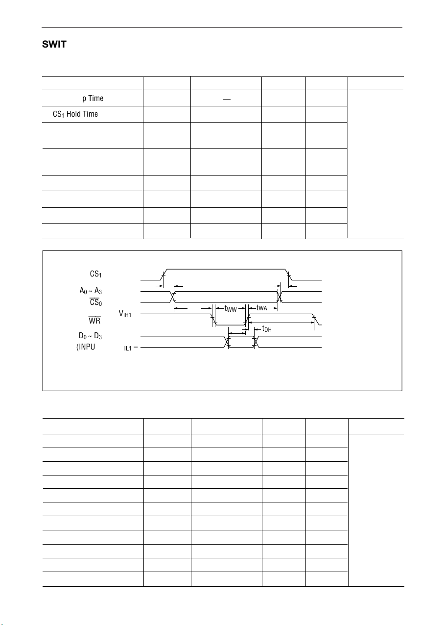
SWITCHING CHARACTERISTICS
(1) WRITE mode (ALE = VDD)
Parameter Symbol Condition Min.
CS1 Set up Time
CS1 Hold Time
Address Stable Before
WRITE
Address Stable After
WRITE
WRITE Pulse Width
Data Set up Time
Data Hold Time
RD / WR Recovery Time
t
t
t
t
t
t
WW
t
t
RCV
C1S
C1H
AW
WA
DS
DH
¡ SemiconductorMSM6242B
(VDD = 5V ± 10% Ta = -40 to +85°C)
Max.
—
—
—
—
—
—
—
—
1000
1000
20
10
120
100
10
60
—
—
—
—
—
—
—
—
Unit
ns
CS
A0 ~ A
CS
WR
D0 ~ D
(INPUT)
V
1
3
0
3
–
IH2
–
V
IH1
V
–
IL1
V
–
IH1
V
–
IH1
–
V
IL1
(2) WRITE mode (With use of ALE)
Parameter Symbol Condition Min.
CS1 Set up Time
Address Set up Time
Address Hold Time
ALE Pulse Width
ALE Before WRITE
WRITE Pulse Width
ALE After WRITE
DATA Set up Time
DATA Hold Time
CS1 Hold Time
RD / WR Recovery Time
t
C1S
t
AW
t
WW
t
DS
t
WA
t
RCV
t
DH
Figure 4. Write Cycle — (ALE = VDD)
t
C1S
t
AS
t
AH
t
AW
t
ALW
t
WW
t
WAL
t
DS
t
DH
t
C1H
t
RCV
—
—
—
—
—
—
—
—
—
—
—
1000
120
100
1000
t
C1H
V
= 2.2V
IH1
V
= 0.8V
IL1
V
= 4/5V
IH2
V
= 1/5V
IL2
(VDD = 5V ± 10%, Ta = -40 ~ +85°C)
Max.
—
25
25
40
10
20
10
60
—
—
—
—
—
—
—
—
—
—
Unit
DD
DD
ns
28
 Loading...