OKI MSM5259GS-L2, MSM5259GS-2L2, MSM5259GS-K, MSM5259GS-2K Datasheet

E2B0019-27-Y2
¡ Semiconductor
This version: Nov. 1997
Previous version: Mar. 1996
MSM5259¡ Semiconductor
MSM5259
40-DOT SEGMENT DRIVER
GENERAL DESCRIPTION
The MSM5259 is a dot matrix LCD segment driver which is fabricated using low power CMOS
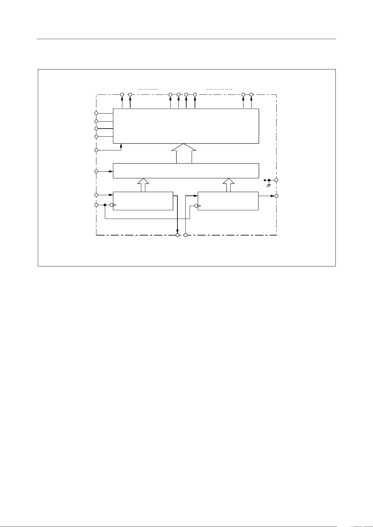
metal gate technology. This LSI consists of 40-bit shift register, 40-bit latch and 40-bit 4-level
driver.
It converts serial data, which is received from an LCD controller LSI, to parallel data and outputs
LCD driving waveforms to LCD.
Expansion of the display can be easily made according to the number and structure of characters.
Since the 40-bit shift register of this device consists of two 20-bit shift registers, it is possible to
allot bits efficiently according to the number of characters.
The MSM5259 can drive a variety of LCD panels because the bias voltage, which determines the
LCD driving voltage, can be optionally supplied from the external source. For static operation
only, the device is available with a power supply voltage of 2.5V or more.
FEATURES
• Supply voltage : 3.5 to 6.0V (Dynamic display)
: 2.5 to 6.0V (Static display)
• LCD driving voltage : 2.5 to 6.0V (Static display)
• Applicable LCD duty : 1/8 to 1/16
• Interface with MSM6222-xx (Dot matrix LCD controller with 16-dot common driver and 40-
dot segment driver)
• Bias voltage can be supplied externally.
• Package options:
56-pin plastic QFP (QFP56-P-910-0.65-K) (Product name : MSM5259GS-K)
56-pin plastic QFP (QFP56-P-910-0.65-L2) (Product name : MSM5259GS-L2)
56-pin plastic QFP (QFP56-P-910-0.65-2K) (Product name : MSM5259GS-2K)
56-pin plastic QFP (QFP56-P-910-0.65-2L2) (Product name : MSM5259GS-2L2)
1/18

BLOCK DIAGRAM
MSM5259¡ Semiconductor
V
DD
V
2
V
3
V
5
DF
LOAD
DI
1
CP
O
O
1
2
20-Bit Shift
Register
O19O20O21O
22
40-Bit 4-Level Driver
40-Bit Latch
DO
20DI21
O
20-Bit Shift
Register
O
40
39
V
SS
DO
40
2/18

PIN CONFIGURATION
MSM5259¡ Semiconductor
(Top View)
NC
56555453525150494847464544
1
O
1
O
2
2
O
3
3
4
O
4
5
O
5
6
O
6
7
O
7
8
O
8
9
O
9
10
O
10
11
O
11
12
O
12
13
O
13
14
O
14
15161718192021222324252627
15
O18O17O16O
CP
)
20
19
DD
O
O
1
LOAD
DI
DF
NC
NC
*(V
NC : No connection
56-Pin Plastic QFP (Type K)
DD
V
21
O
2
V
VSSV
23
22
O
20
5
3
O24O
DI 21DO
V
43
42
DO
40
O
41
40
O
40
39
39
O
38
38
O
37
37
O
36
36
O
35
35
O
34
34
O
33
33
O
32
32
O
31
31
O
30
30
O
29
29
O
28
28
27O26
25
O
O
NC
NC
NC
DF
LOAD
DI
CP
V
DD
V
SS
V
V
V
DO
DI
5
8
1
123456789
56
55
54
53
52
51
50
49
48
47
2
46
3
45
5
44
20
43
21
42414039383736353433323130
40
40
DO
6
7
O
O
O
O4O3O2O
O38O39O
O
36
37
O
O34O35O
NC : No connection
56-Pin Plastic QFP (Type L)
10
11
O
O9O
1011121314
32
33
O31O
O
O
12
O14O13O
15
O
15
O
16
16
O
17
17
18
O
18
19
O
19
20
O
20
21
*(VDD)
22
O
21
23
O
22
24
O
23
25
O
24
26
O
25
27
O
26
28
O
27
29
29
30
O28O
* Do not connect pin 21 to the other signal pins, because the pin is internally connected to VDD.
Do not use pin 21 as a single VDD signal line. It is permissible to use pin 21 for supplying a
higher power of VDD.
Note : The figure for Type L shows the configuration viewed from the reverse side of the package.
Pay attention to the difference in pin arrangement.
3/18

ABSOLUTE MAXIMUM RATINGS
MSM5259¡ Semiconductor
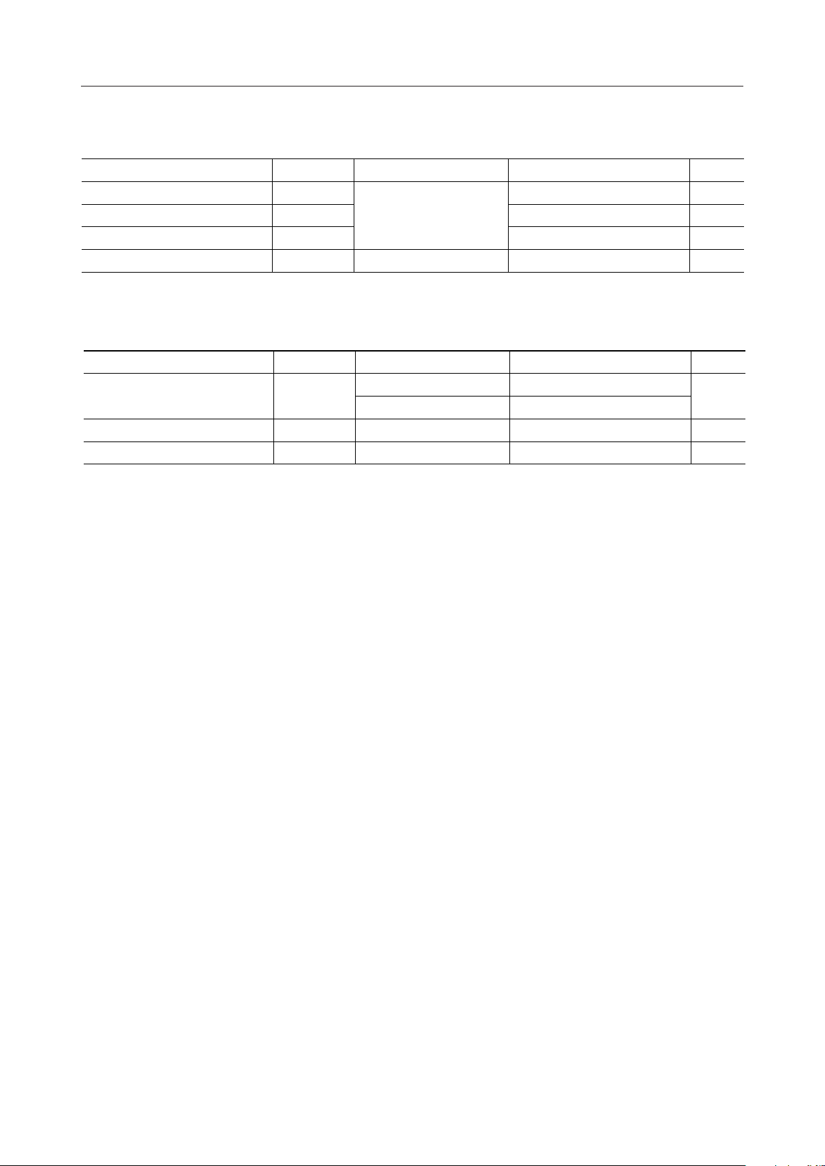
Parameter
Supply Voltage (1)
Supply Voltage (2) V
Input Voltage V
Storage Temperature T
Symbol Condition Rating Unit
–0.3 to +6.5 V
–0.3 to V
DD
DD
V
DD
–
STG
*1
V
5
I
Ta = 25°C 0 to +6.5 V
— –55 to +150 °C
RECOMMENDED OPERATING CONDITIONS
Parameter
Supply Voltage (1)
Supply Voltage (2) V
Operating Temperature T
*1 VDD > V2 > V3 > V5 > VSS (Dynamic display)
VDD = V3 > V2 = V5 = VSS (Static display)
For VDD of less than 3.5V, the device is available only for static operation.
*2 VDD is the reference potential for the LCD driving voltage.
To determine the LCD driving voltage, change the value of V5. (0V Minimum)
Symbol Condition Rnage Unit
3.5 to 6.0
2.5 to 6.0 V
DD
DD
–
op
V
5
Static 2.5 to 6.0
—*1 *2
— –30 to +85 °C
V
Dynamic
+0.3 V
V
4/18

ELECTRICAL CHARACTERISTICS
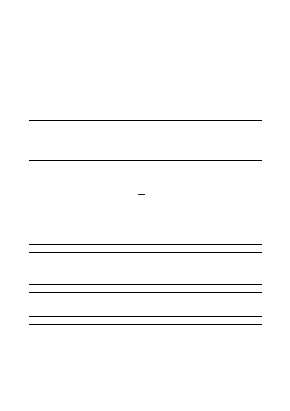
DC Characteristics (1)
Parameter
"H" Input Voltage
"L" Input Voltage V
"H" Input Current I
"L" Input Current I
"H" Output Voltage V
"L" Output Voltage V
ON Resistance R
Symbol Condition Min. Typ. Max. Unit
V
*1
IH
*1
IL
*1
IH
*1
IL
*2
OH
*2
OL
*3
ON
MSM5259¡ Semiconductor
= 5V±10%, Ta=–30 to +85°C)
(V
DD
— 0.8V
DD
— 0 — 0.2V
V
= V
IH
DD
V
= 0V — — –1 mA
IL
I
= –40mA 4.2 — — V
O
I
= 0.4mA — — 0.4 V
O
—— 1 mA
VDD–V5= 5V
|V
N–VO
| = 0.25V
—— 5 kW
*4
—VDDV
DD
V
Supply Current I
DD
f
= 0Hz, No load — — 0.5 mA
CP
*1 Applicable to DF, LOAD, DI1 and DI21.
*2 Applicable to DO20 and DO40.
*3 Applicable to O1 to O40.
*4 Dynamic display : VN = VDD to V5, V2 = (VDD – V5), V3 = (VDD – V5)
Static display : VN = VDD to V5, V3 = VDD, V2 = V5 = V
2
3
SS
1
3
DC Characteristics (2)
(Only for static operation)
Parameter
Symbol Condition Min. Typ. Max. Unit
"H" Input Voltage
"L" Input Voltage V
"H" Input Current I
"L" Input Current I
"H" Output Voltage V
"L" Output Voltage V
ON Resistance R
Supply Current I
V
*1
IH
*1
IL
V
IH
IL
OH
OL
*1
*1
*5
*5
= V
IH
DD
V
= 0V — — –1 mA
IL
I
= –40mA 2.2 — — V
O
I
= 0.2mA — — 0.4 V
O
— 0.8V
— 0 — 0.2V
V3 = VDD = 3V, V2 = V5 = VSS = 0V,
*6
ON
| VN–VO | = 0.25V
DD
fCP = 0Hz, No load — — 0.5 mA
= 3V±0.5V, Ta=–30 to +85°C)
(V
DD
DD
—VDDV
—— 1 mA
——10kW
DD
V
*5 Applied to DO20 and DO40.
*6 Applied to O1 to O40.
5/18

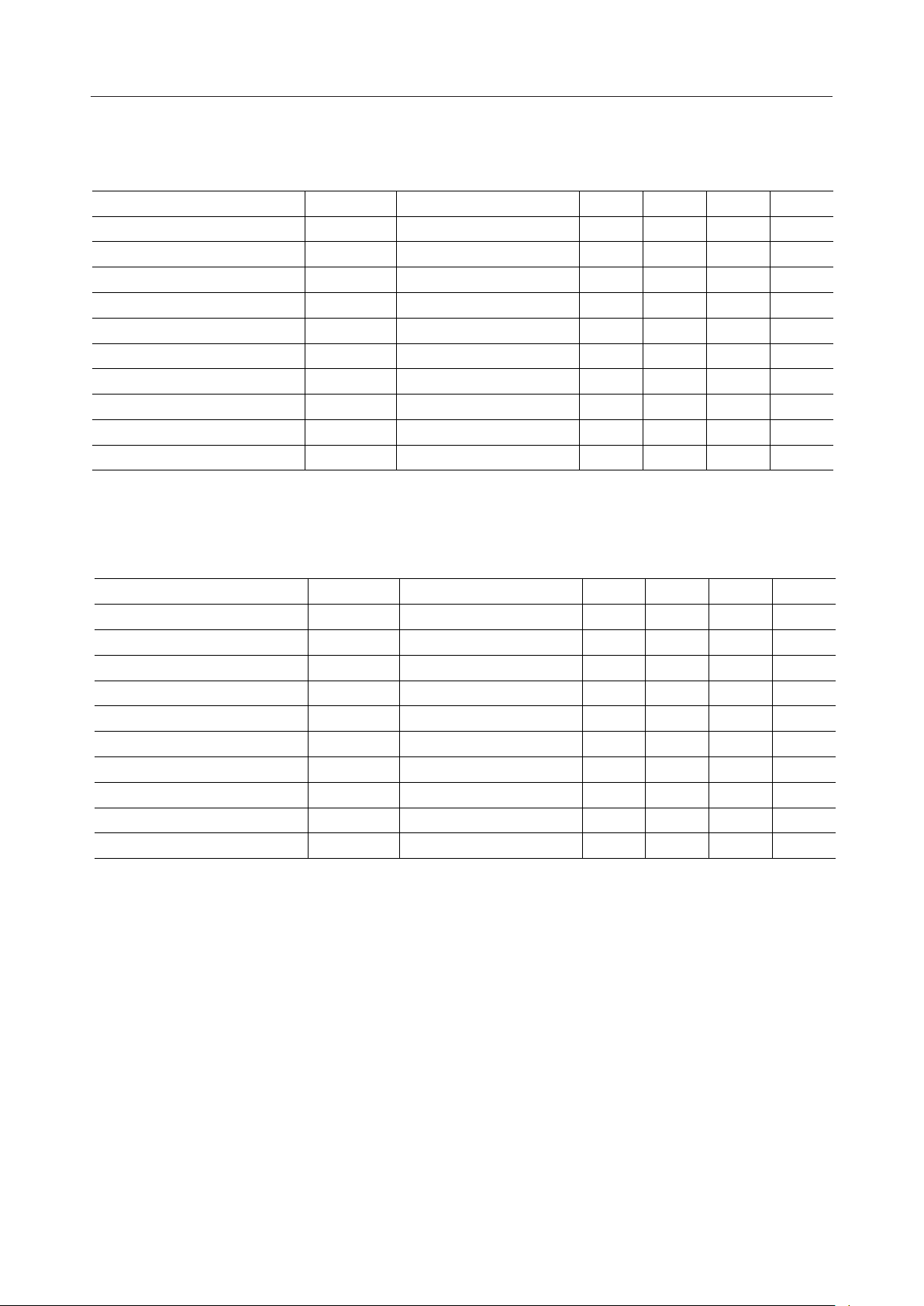
Switching Characteristics (1)
Parameter
"H", "L" Propagation Delay Time
Clock Frequency f
Clock Pulse Width t
Load Pulse Width t
Data Set-up Time DI
Data Hold Time DI
CP t
Æ
CP t
Æ
CP Æ LOAD Set-up Time t
LOAD Æ CP Hold Time t
CP Rise/Fall Time t
LOAD Rise/Fall Time t
Symbol Condition Min. Typ. Max. Unit
t
r(CP)
Switching Characteristics (2)
PLH, tPHL
CP
W (CP)
W (L)
SETUP
HOLD
CL
LC
, t
(CP)
f
, t
r(L)
f(L)
MSM5259¡ Semiconductor
(V
= 5V±10%, Ta=–30 to +85°C, CL=15pF)
DD
— — — 250 ns
Duty = 50% — — 3.3 MHz
—
—
—
—
—
—
—
—
125 — — ns
125 — — ns
50——ns
50——ns
250 — — ns
0——ns
——50ns
—— 1 ms
(Only for static operation)
Parameter
"H", "L" Propagation Delay Time
Symbol Condition Min. Typ. Max. Unit
t
PLH, tPHL
Clock Frequency f
Clock Pulse Width t
Load Pulse Width t
DI Æ CP Set-up Time t
DI Æ CP Hold Time t
CP Æ LOAD Set-up Time t
LOAD Æ CP Hold Time t
CP Rise/Fall Time t
LOAD Rise/Fall Time t
r(L)
CP
W (CP)
W (L)
SETUP
HOLD
CL
LC
r(CP)
, t
f(L)
(V
= 3V±0.5V, Ta=–30 to +85°C, CL=15pF)
DD
— — — 800 ns
Duty = 50% — — 1.0 MHz
—
—
—
—
—
—
—
—
300 — — ns
300 — — ns
200 — — ns
200 — — ns
800 — — ns
0——ns
—— 1 ms
—— 1 ms
6/18
 Loading...