

OKI MR27V3202DTA, MR27V3202DMA Datasheet

1/11
¡
The MR27V3202D is a 32Mbit electrically Programmable Read-Only Memory whose configuration
can be electrically switched between 2,097,152 word x 16bit and 4,194,304 word x 8bit. The MR27
V3202D operates on a single +3V-3.3V power supply and is TTL compatible. Since the MR27V3202
D operates asynchronously , external clocks are not required , making this device easy-to-use. The
MR27V3202D is suitable as large-capacity fixed memory for microcomputers and data terminals. It
is manufactured using a CMOS double silicon gate technology and is offered in 44-pin SOP or 48pin TSOP packages.
1A
MR27V3202D
2,097,152-Word x 16-Bit or 4,194,304-Word x 8-Bit One Time PROM
DESCRIPTION
FEATURES
• 2,097,152 word x 16bit / 4,194,304 word x 8bit electrically switchable configuration
• Single +3V-3.3V power supply
• Access time 120ns access time (Vcc=+3V)
100ns access time (Vcc=+3.3V)
• Input / Output TTL compatible
• Three-state output
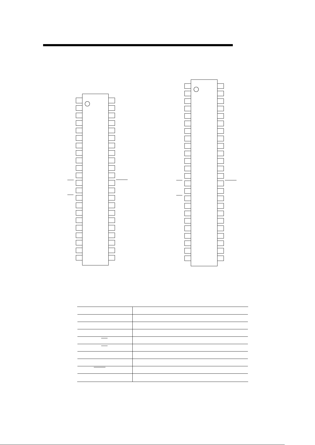
• Packages
44-pin plastic SOP (SOP44-P-600-1.27-K) (Product name : MR27V3202DMA)
48-pin plastic TSOP (TSOP II 48-P-550-0.80-K) (Product name : MR27V3202DTA)
Semiconductor
November 1999
2/11
PIN NAMES
FUNCTIONS
D15/A-1 Data output / Address input
A0-A20 Address input
D0-D14 Data output
CE
OE
Output enable
V
CC
Power supply voltage
BYTE/V
PP
Mode switch / Program power supply voltage
NC
Non connection
PIN CONFIGURATION (TOP VIEW)
Chip enable
V
SS
GND
MR27V3202D
45
A18
A8
A9
A11
A12
A13
A14
A15
A16
V
SS
D15/A-1
D7
D14
D6
D13
D5
D12
D4
V
CC
A10
44
43
42
4
5
6
7
41
40
39
38
8
9
10
11
37
36
35
34
12
13
14
15
33
32
31
30
16
17
18
19
29
28
27
26
20
21
22
23
2524
A19
A17
A7
A6
A5
A4
A3
A2
A1
A0
CE
V
SS
OE
D0
D8
D1
D9
D2
D10
D3
D11
48
NC
NC
47
1
2
NC
NC
NC
463
43
A18
A8
A9
A11
A12
A13
A14
A15
A16
V
SS
D15/A-1
D7
D14
D6
D13
D5
D12
D4
V
CC
A10
42
41
40
2
3
4
5
39
38
37
36
6
7
8
9
35
34
33
32
10
11
12
13
31
30
29
28
14
15
16
17
27
26
25
24
18
19
20
21
2322
A19
A17
A7
A6
A5
A4
A3
A2
A1
A0
CE
V
SS
OE
D0
D8
D1
D9
D2
D10
D3
D11
44
NC
1
BYTE/Vpp
BYTE/Vpp
48-pin TSOP (II)44-pin SOP
A20
A20
3/11
A0
A1
A2
A3
A4
A5
A6
A7
A8
A9
A10
A11
A12
A13
A14
A15
A16
A17
A18
A19
A20
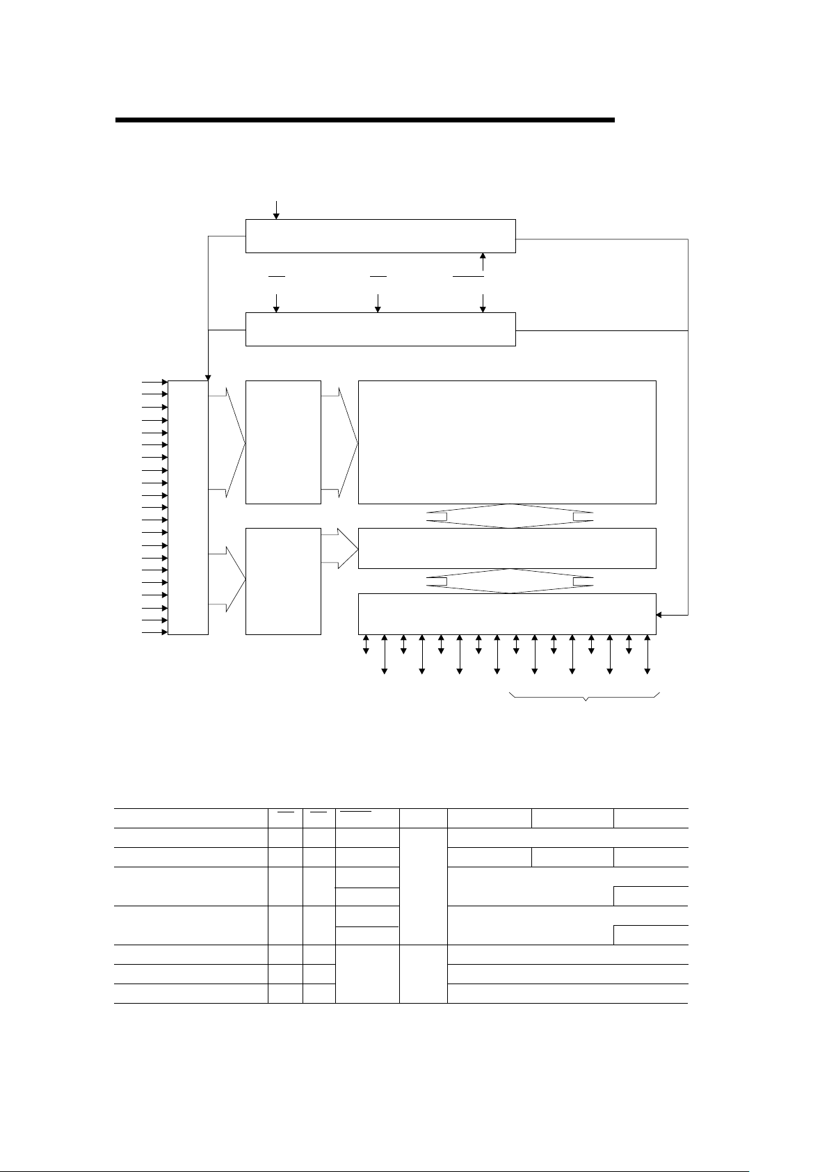
BLOCK DIAGRAM
D0
CE BYTE/V
PP
OE
CE PGMOE
Address Buffer
Row Decoder
Column Decoder
Memory Matrix
Multiplexer
Output Buffer
FUNCTION TABLE
STAND-BY
OUTPUT DISABLE
READ (8-Bit)
READ (16-Bit)
MODE
D15/A-1
CE OE
V
CC
LL
D
OUT
L
L
L/H
L
H
L
*
H
*
H
L
*: Don't Care
D1D2D3D4D5D6D7D8D9
D10
D11
D12
D13
D14
D15
X8/X16 Switch
A-1
In 8-bit output mode, these pins are
three-stated and pin D15 functions
as the A-1 address pin.
3.0V
to
3.3V
D8 - D14D0 - D7
H
L
D
OUT
Hi-Z
H
Hi-Z
*
Hi-Z
PROGRAM
LH
D
IN
PROGRAM INHIBIT
H H Hi-Z
PROGRAM VERIFY
HL
D
OUT
9.75V
4.0V
MR27V3202D
BYTE/V
PP
2,097,152X16-Bit or 4,194,304X8-Bit
4/11
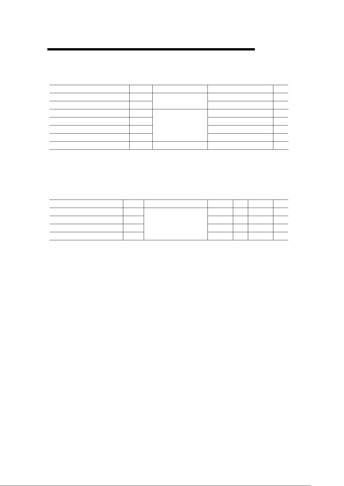
Operating temperature under bias
Storage temperature
Input voltage
Output voltage
Power supply voltage
Program power supply voltage
Power dissipation per package
Parameter
Symbol
Topr
UnitValueCondition
RECOMMENDED OPERATING CONDITIONS
VCC power supply voltage
VPP power supply voltage
Input "H" level
Input "L" level
Parameter Symbol
V
CC
Unit
3.6
Typ.
2.7
Condition
T
stg
V
I
V
O
V
CC
V
PP
P
D
0 to 70
-55 to 125
V-0.5 to V
CC
+ 0.5
V-0.5 to VCC +0.5
V-0.5 to 5
V-0.5 to 11.5
W1.0
-
relative to V
SS
(Ta=0 to 70°C)
Min. Max.
V
V
CC
+0.5
-0.5
-
V
V
CC
+0.5*2.2
-
V
0.6-0.5**
-
V
V
PP
V
IH
V
IL
VCC=2.7V-3.6V
Voltage is relative to Vss
ABSOLUTE MAXIMUM RATINGS
-
-
MR27V3202D
°C
°C
* : Vcc+1.5V (Max.) when pulse width of overshoot is less than 10nS.
** : -1.5V (Min.) when pulse width of undershoot is less than 10nS.
 Loading...