

OKI MR27V1602ETN, MR27V1602ETP, MR27V1602EMA Datasheet

PEDR27V1602E-01-01
1
Semiconductor
This version : Dec. 1999
Previous version: ----------
MR27V1602E
Preliminary
1,048,576–Word ×××× 16–Bit or 2,097,152–Word ×××× 8–Bit One Time PROM
1/11
GENERAL DESCRIPTION
The MR27V1602E is a 16 Mbit electrically Programmable Read-Only Memory that can be electrically switched
between 1,048,576-word × 16-bit and 2,097,152-word × 8-bit configurations. This device operates on a single
+3.3V power supply, and all inputs and outputs are TTL compatible. Because of its asynchronous operation, it
requires no external clocks, making this device easy-to-use.
The MR27V1602E is suitable as large-capacity fixed memory for microcomputers and data terminals. It is
manufactured using a CMOS double silicon gate technology and is offered in 44-pin SOP, 44-pin TSOP(II) or
48-pin TSOP(I) packages.
FEATURES
∙ 1,048,576-word × 16-bit/2,097,152-word × 8-bit electrically switchable configuration
∙ +3.3 V power supply
∙ Access time 90 nS MAX
∙ Operating current 30 mA MAX
∙ Standby current 50 µA MAX
∙ Input/Output TTL compatible
∙ Three-state output
∙ Packages:
44-pin plastic SOP (SOP44-P-600-1.27-K) (Product Name : MR27V1602EMA)
44-pin plastic TSOP (TSOP II 44-P-400-0.80-K) (Product Name : MR27V1602ETP)
48-pin plastic TSOP (TSOP I 48-P-1220-0.50-K) (Product Name : MR27V1602ETN)

PEDR27V1602E-01-01
1
Semiconductor
MR27V1602E
2/11
PIN CONFIGURATION (TOP VIEW)
Pin name Functions
D15/A–1 Data output/Address input
A0 to A19 Address input
D0 to D14 Data output
CE Chip enable
OE Output enable
BYTE/V
PP
Mode switch/Program power supply voltage
V
CC
Power supply voltage
V
SS
GND
NC Non connection
1
2
3
4
5
6
7
8
9
10
11
12
13
14
15
16
17
18
19
20
21
22
44
43
42
41
40
39
38
37
36
35
34
33
32
31
30
29
28
27
26
25
24
23
NC
A19
A8
A9
A10
A11
A12
A13
A14
A15
A16
BYTE/V
PP
V
SS
D15/A–1
D7
D14
D6
D13
D5
D12
D4
V
CC
NC
A18
A17
A7
A6
A5
A4
A3
A2
A1
A0
CE
V
SS
OE
D0
D8
D1
D9
D2
D10
D3
D11
44-pin SOP, TSOP(II
)
1
2
3
4
5
6
7
8
9
10
11
12
13
14
15
16
17
18
19
20
21
22
23
24
48
47
46
45
44
43
42
41
40
39
38
37
36
35
34
33
32
31
30
29
28
27
26
25
A15
A14
A13
A12
A11
A10
A9
A8
A19
NC
NC
NC
NC
NC
NC
A18
A17
A7
A6
A5
A4
A3
A2
A1
A16
BYTE/V
PP
V
SS
D15/A–1
D7
D14
D6
D13
D5
D12
D4
V
CC
D11
D3
D10
D2
D9
D1
D8
D0
OE
V
SS
CE
A0
48-pin TSOP(I
)
PEDR27V1602E-01-01
1
Semiconductor
MR27V1602E
3/11
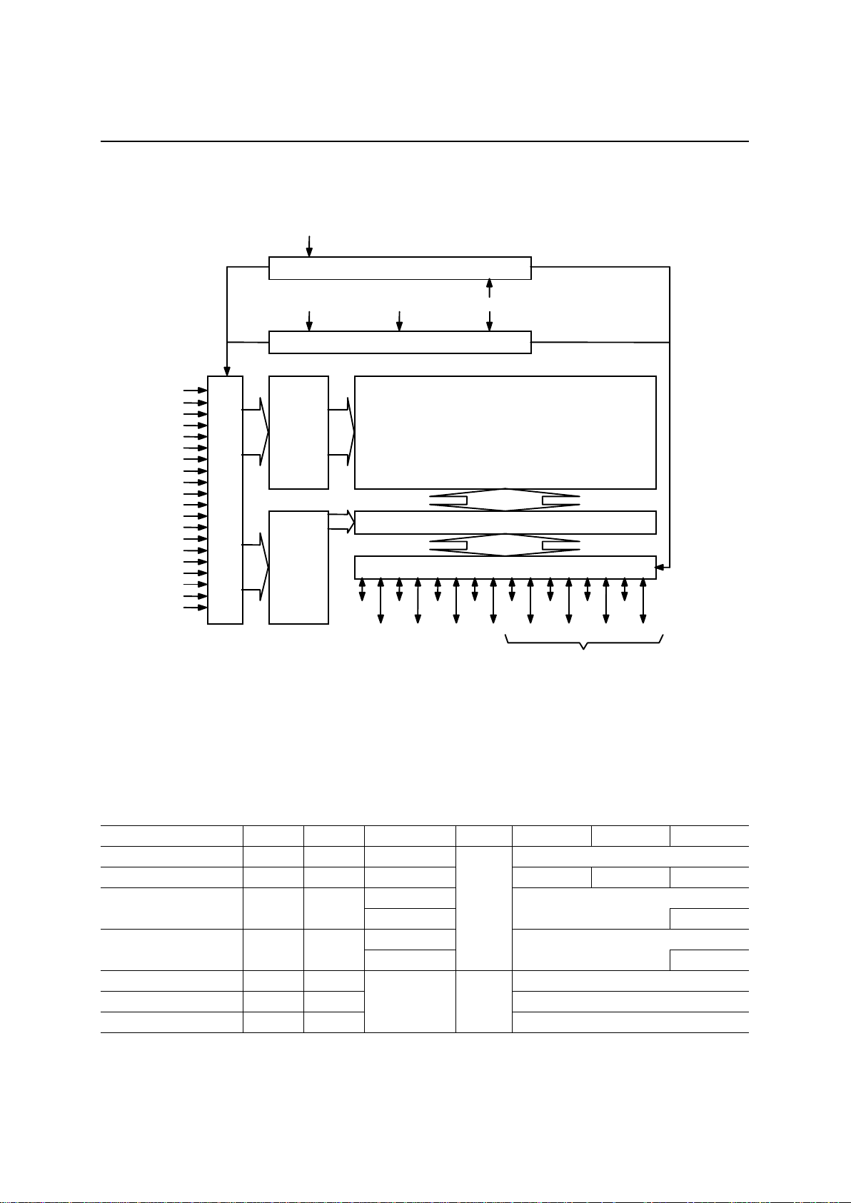
BLOCK DIAGRAM
FUNCTION TABLE
Mode CE OE BYTE/V
PP
V
CC
D0 to D7 D8 to D14 D15/A–1
Read (16-Bit) L L H D
OUT
Read (8-Bit) L L L D
OUT
Hi–Z L/H
H
Output disable L H
L
Hi–Z
∗
H
Standby H ∗
L
3.3 V
Hi–Z
∗
Program L H D
IN
Program inhibit H H Hi–Z
Program verify H L
9.75 V 4.0 V
D
OUT
∗
: Don’t Care (H or L)
A0
A1
A2
A3
A4
A5
A6
A7
A8
A9
A10
A11
A12
A13
A14
A15
A16
A17
A18
A19
CE BYTE/V
PP
OE
CE PGMOE
× 8/× 16 Switch
D0 D2 D4 D6 D8 D10 D12 D14
D1 D3 D5 D7 D9 D11 D13 D15
Memory Cell Matrix
1,048,576 × 16-Bit or 2,097,152 × 8-Bit
Multiplexer
Output Buffer
Row Decoder
Column Decoder
Address Buffer
In 8-bit output mode, these pins
are three-stated and pin D15
functions as the A-1 address pin.
A–1
PEDR27V1602E-01-01
1
Semiconductor
MR27V1602E
4/11
ABSOLUTE MAXIMUM RATINGS
Parameter Symbol Condition Value Unit
Operating temperature under bias Ta 0 to 70 °C
Storage temperature Tstg
—
–55 to 125 °C
Input voltage V
I
–0.5 to VCC+0.5 V
Output voltage V
O
–0.5 to VCC+0.5 V
Power supply voltage V
CC
–0.5 to 5 V
Program power supply voltage V
PP
relative to V
SS
–0.5 to 11.5 V
Power dissipation per package P
D
—1.0W
RECOMMENDED OPERATING CONDITIONS
(Ta = 0 to 70°C)
Parameter Symbol Condition Min. Typ. Max. Unit
VCC power supply voltage V
CC
3.0 — 3.6 V
VPP power supply voltage V
PP
–0.5 — VCC+0.5 V
Input “H” level V
IH
2.2 — V
CC
+0.5∗ V
Input “L” level V
IL
VCC = 3.0 to 3.6 V
–0.5∗∗ —0.6 V
Voltage is relative to VSS.
∗
: Vcc+1.5V(Max.) when pulse width of overshoot is less than 10ns.
∗∗
: -1.5V(Min.) when pulse width of undershoot is less than 10ns.
 Loading...