

A
A
A8 A9 A
A
A
A
A
A
A
查询MR27T802F供应商
OKI Semiconductor
FEDR27T802F-02-05
Issue Date: Dec. 28, 2004
MR27T802F
512k–Word × 16–Bit or 1M–Word × 8–Bit P2ROM
FEATURES
·512k-word × 16-bit / 1M-word × 8-bit electrically switchable
configuration
· +2.7 V to 3.6 V power supply
· Access time 80 ns MAX
· Operating current 18 mA MAX(5MHz)
· Standby current 5 µA MAX
· Input/Output TTL compatible
· Three-state output
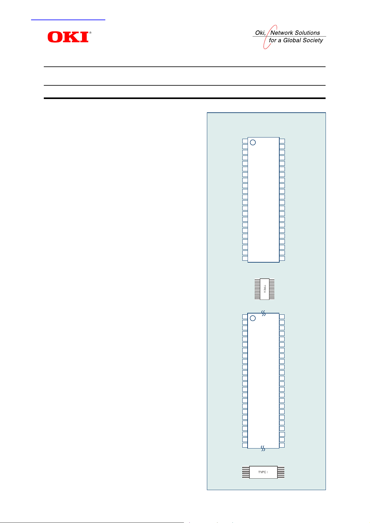
PACKAGES
· MR27T802F-xxxTN
48-pin plastic TSOP (TSOP I 48-P-1220-0.50-1K)
· MR27T802F-xxxMA
44-pin plastic SOP (SOP44-P-600-1.27-K)
· MR27T802F-xxxTP
44-pin plastic TSOP (TSOP II 44-P-400-0.80-K)
P2ROM ADVANCED TECHNOLOGY
P2ROM stands for Production Programmed ROM. This
exclusive Oki technology utilizes factory test equipment for
programming the customers code into the P 2ROM pri or to final
production testing. Advancements in this technology allows
production costs to be equivalent to MASKR OM and has many
advantages and added benefits over the other non-volatile
technologies, which include the following;
· Short lead time, since the P2ROM is programmed at the
final stage of the production process, a large P2ROM
inventory "bank system" of un-programmed packaged
products are maintained to provide an aggressive lead-time
and minimize liability as a custom product.
· No mask charge, since P2ROMs do not utilize a custom
mask for storing customer code, no mask charges apply.
· No additional programming charge, unlike Flash and
OTP that require additional programming and handling
costs, the P2ROM already has the code loaded at the factory
with minimal effect on the production throughput. The cost
is included in the unit price.
· Custom Marking is available at no additional charge.
· Pin Compatible with Mask ROM and some FLASH
products.
PIN CONFIGURATION (TOP VIEW)
1
NC
2
A18
3
A17
4
A7
5
A6
6
A5
7
A4
8
A3
9
A2
10
A1
11
A0
12
CE#
13
V
SS
14
OE#
15
D0
16
D8
17
D1
18
D9
19
D2
20
D10
21
D3
22
D11
44SOP,
44TSOP(Type-II)
1
A15
2
A14
3
A13
4
A12
5
A11
6
A10
7
A9
8
A8
9
NC
10
NC
11
NC
12
NC
13
NC
14
NC
15
NC
16
A18
17
A17
18
A7
19
A6
20
A5
21
A4
22
A3
23
A2
24
A1
48TSOP(Type-I)
44
NC
43
NC
42
41
40
10
39
11
38
12
37
13
36
14
35
15
34
16
33
BYTE#
32
VSS
31
D15/A–1
30
D7
29
D14
28
D6
27
D13
26
D5
25
D12
24
D4
23
VCC
48
16
47
BYTE#
46
VSS
45
D15/A–1
44
D7
43
D14
42
D6
41
D13
40
D5
39
D12
38
D4
37
V
CC
36
D11
35
D3
34
D10
33
D2
32
D9
31
D1
30
D8
29
D0
28
OE#
27
V
SS
26
CE#
25
0
1/10
FEDR27T802F-02-05
OKI Semiconductor
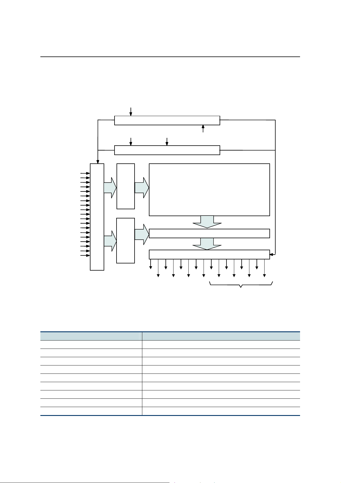
BLOCK DIAGRAM
A0
A1
A2
A3
A4
A5
A6
A7
A8
A9
A10
A11
A12
A13
A14
A15
A16
A17
A18
PIN DESCRIPTIONS
Pin name Functions
D15 / A–1 Data output / Address input
A0 to A18 Address inputs
D0 to D14 Data outputs
CE# Chip enable input
OE# Output enable input
BYTE# Word / Byte select input
VCC Power supply voltage
VSS Ground
NC No connect
MR27T802F / P2ROM
A–1
× 8/× 16 Switch
CE# BYTE# OE#
CE OE
Memory Cell Matrix
Row Decoder
Address Buffer
Column Decoder
D0 D2 D4 D6 D8 D10 D12 D14
D1 D3 D5 D7 D9 D11 D13 D15
512k × 16-Bit or 1M × 8-Bit
Multiplexer
Output Buffer
In 8-bit output mode, these pins
are placed in a high-Z state and
pin D15 functions as the A-1
address pin.
2/10
FEDR27T802F-02-05
OKI Semiconductor
MR27T802F / P2ROM
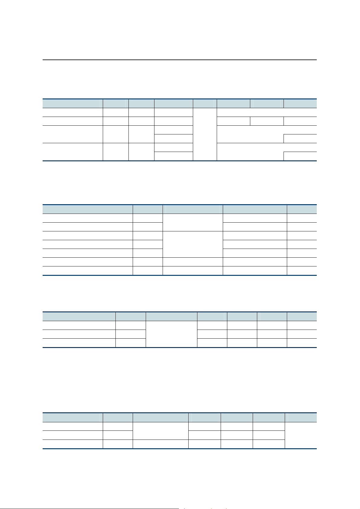
FUNCTION TABLE
Mode CE# OE# BYTE# VCC D0 to D7 D8 to D14 D15/A–1
Read (16-Bit) L L H D
Read (8-Bit) L L L D
Output disable L H
Standby H ∗
H
L
H
L
3.0V
Hi–Z L/H
OUT
OUT
Hi–Z
Hi–Z
∗
∗
∗: Don’t Care (H or L)
ABSOLUTE MAXIMUM RATINGS
Parameter Symbol Condition Value Unit
Operating temperature under bias Ta 0 to 70 °C
Storage temperature Tstg
Input voltage VI –0.5 to VCC+0.5 V
Output voltage VO –0.5 to VCC+0.5 V
Power supply voltage VCC
Power dissipation per package PD Ta = 25°C 1.0 W
Output short circuit current IOS — 10 mA
—
relative to V
SS
–55 to 125 °C
–0.5 to 5 V
RECOMMENDED OPERATING CONDITIONS
(Ta = 0 to 70°C)
Parameter Symbol Condition Min. Typ. Max. Unit
VCC power supply voltage VCC 2.7 — 3.6 V
= 2.7 to 3.6 V
Input “H” level VIH 2.2 — VCC+0.5∗ V
Input “L” level VIL
V
CC
–0.5∗∗ — 0.6 V
Voltage is relative to VSS.
∗ : Vcc+1.5V(Max.) when pulse width of overshoot is less than 10ns.
∗∗ : -1.5V(Min.) when pulse width of undershoot is less than 10ns.
PIN CAPACITANCE
(VCC = 3.3 V, Ta = 25°C, f = 1 MHz)
Parameter Symbol Condition Min. Typ. Max. Unit
Input C
BYTE# C
Output C
— — 8
IN1
IN2
V
OUT
V
= 0 V
I
= 0 V — — 10
O
— — 100
pF
3/10

FEDR27T802F-02-05
OKI Semiconductor
MR27T802F / P2ROM
ELECTRICAL CHARACTERISTICS
DC Characteristics
(VCC = 2.7 V to 3.6 V, Ta = 0 to 70°C)
Parameter Symbol Condition Min. Typ. Max. Unit
Input leakage current ILI V
Output leakage current ILO V
I
CE# = VCC — — 5 µA VCC power supply current
CCSC
(Standby)
V
power supply current
CC
(Read)
I
CE# = VIH — — 1 mA
CCST
I
CCA
Input “H” level VIH — 2.2 — VCC+0.5∗ V
Input “L” level VIL — –0.5∗∗ — 0.6 V
Output “H” level VOH I
Output “L” level VOL I
Voltage is relative to VSS.
∗ : Vcc+1.5V(Max.) when pulse width of overshoot is less than 10ns.
∗∗ : -1.5V(Min.) when pulse width of undershoot is less than 10ns.
AC Characteristics
Parameter Symbol Condition Min. Max. Unit
Address cycle time tC — 80 — ns
Address access time t
CE# = OE# = V
ACC
CE# access time tCE OE# = VIL — 80 ns
OE# access time tOE CE# = VIL — 30 ns
t
OE# = VIL 0 20 ns
Output disable time
CHZ
t
CE# = VIL 0 20 ns
OHZ
Output hold time tOH CE# = OE# = V
Measurement conditions
Input signal level --------------------------------------0 V/3 V
Input timing reference level-------------------------1/2Vcc
Output load ---------------------------------------------50 pF
Output timing reference level ----------------------1/2Vcc
Output load
Output
= 0 to VCC — — 5 µA
I
= 0 to VCC — — 5 µA
O
CE# = VIL, OE# = V
tc = 200 ns
= –1 mA 2.4 — — V
OH
= 2 mA — — 0.4 V
OL
IH
— — 18 mA
(VCC = 2.7 V to 3.6 V, Ta = 0 to 70°C)
IL
IL
— 80 ns
0 — ns
50 pF
(Including scope and jig)
4/10

FEDR27T802F-02-05
OKI Semiconductor
TIMING CHART (READ CYCLE)
16-Bit Read Mode (BYTE# = VIH)
A0 to A18
tCE
CE#
tOE
OE#
t
ACC
D0 to D15
8-Bit Read Mode (BYTE# = V
A-1 to A18
Hi-Z
tCE
CE#
t
OE
OE#
t
ACC
D0 to D7
Hi-Z
tC
t
C
Valid Data
)
IL
Valid Data
t
t
OH
OH
t
ACC
t
ACC
MR27T802F / P2ROM
t
C
tOH
t
CHZ
t
OHZ
Valid Data
t
C
Hi-Z
tOH
t
CHZ
t
OHZ
Valid Data
Hi-Z
5/10

FEDR27T802F-02-05
OKI Semiconductor
PACKAGE DIMENSIONS
TSOP(1)48-P-1220-0.50-1K
Mirror finish
MR27T802F / P2ROM
(Unit: mm)
Package material Epoxy resin
Lead frame material 42 alloy
5
Pin treatment
Package weight (g) 0.55 TYP.
Rev. No./Last Revised 1/Dec. 2, 1999
Solder plating (≥5µm)
Notes for Mounting the Surface Mount Type Package
The surface mount type packages are very susceptible to heat in reflow mounting and humidity absorbed in
storage.
Therefore, before you perform reflow mounting, contact Oki’s resp onsible sales person for the product name,
package name, pin number, package code and desired mounting conditions (reflow method, temperature and
times).
6/10

FEDR27T802F-02-05
OKI Semiconductor
SOP44-P-600-1.27-K
Mirror finish
5
MR27T802F / P2ROM
(Unit: mm)
Package material Epoxy resin
Lead frame material 42 alloy
Pin treatment
Package weight (g) 2.10 TYP.
Rev. No./Last Revised 4/Dec. 5, 1996
Solder plating (≥5µm)
Notes for Mounting the Surface Mount Type Package
The surface mount type packages are very susceptible to heat in reflow mounting and humidity absorbed in
storage.
Therefore, before you perform reflow mounting, contact Oki’s resp onsible sales person for the product name,
package name, pin number, package code and desired mounting conditions (reflow method, temperature and
times).
7/10

FEDR27T802F-02-05
OKI Semiconductor
TSOP(2)44-P-400-0.80-K
Mirror finish
MR27T802F / P2ROM
(Unit: mm)
Package material Epoxy resin
Lead frame material 42 alloy
5
Pin treatment
Package weight (g) 0.54 TYP.
Rev. No./Last Revised 3/Dec. 10, 1996
Solder plating (≥5µm)
Notes for Mounting the Surface Mount Type Package
The surface mount type packages are very susceptible to heat in reflow mounting and humidity absorbed in
storage.
Therefore, before you perform reflow mounting, contact Oki’s resp onsible sales person for the product name,
package name, pin number, package code and desired mounting conditions (reflow method, temperature and
times).
8/10

FEDR27T802F-02-05
OKI Semiconductor
MR27T802F / P2ROM
REVISION HISTORY
Edition
Page
Current
Edition
Description
Change Operating temperature under bias
(Ta) to 0 to 70°C.
Document
No.
FEDR27T802F-02-01 Dec., 2002 – – Final edition 1
FEDR27T802F-02-02 Jun. 17, 2003 3, 4 3, 4
FEDR27T802F-02-03 Jul. 9, 2004 3 3 Add PD condition and IOS = 10mA
FEDR27T802F-02-04 Sep. 3, 2004 1 1, 7 Add MR27T802F-xxxMA
FEDR27T802F-02-05 Dec. 28, 2004 1 1, 8 Add MR27T802F-xxxTP
Date
Previous
9/10

FEDR27T802F-02-05
OKI Semiconductor
MR27T802F / P2ROM
NOTICE
1. The information contained herein can change without notice owing t o pr o duct and/or technical improvements.
Before using the product, please make sure that the information being referred to is up-to-date.
2. The outline of action and examples for application circuits described herein have been chosen as an explanation
for the standard action and performance of the p roduct. When planning to use the product, please ensure that the
external conditions are reflected in the actual circuit, assembly, and program designs.
3. When designing your product, please use our product below the specified maximum ratings and within the
specified operating ranges including, but not limited to, operating voltage, power dissipation, and operating
temperature.
4. Oki assumes no responsibility or liability whatsoever for any failure or unusual or unexpected operation
resulting from misuse, neglect, improper installation, repair, alteration or accident, improper handling, or
unusual physical or electrical stress including, but not limited to, expo sure to p arameters beyond the specified
maximum ratings or operation outside the specified operating range.
5. Neither indemnity against nor license of a third part y’s i ndustrial and intellectual property right, etc. is granted
by us in connection with the use of the product and/or the information and drawings contained herein. No
responsibility is assumed by us for any infringement of a third party’s right which may result from the use
thereof.
6. The products listed in this document are intended for use in general electronics equipment for commercial
applications (e.g., office automation, communication equipment, measurement equipment, consumer
electronics, etc.). These products are not, unless specifically authorized by Oki, authorized for use in any
system or application that requires special or enhanced quality and reliability characteristics nor in any system
or application where the failure of such system or application may result in the loss or damage of property, or
death or injury to humans.
Such applications include, but are not limited to, traffic and automotive equipment, safety devices, aerospace
equipment, nuclear power control, medical equipment, and life-support systems.
7. Certain products in this document may need government approval before they can be exported to particular
countries. The purchaser assumes the responsibility of determining the legality of export of these products and
will take appropriate and necessary steps at their own expense for these.
8. No part of the contents contained herein may be reprinted or reproduced without our prior permission.
Copyright 2004 Oki Electric Industry Co., Lt d.
10/10
 Loading...