

c
A
A
A
A
A
A
A
A
A
A
A
A
A
查询MR27T401E供应商
OKI Semiconductor
FEDR27T401E-02-01
Issue Date: Apr. 17, 2002
MR27T401E
512K–Word × 8–Bit P2ROM
FEATURES
·524,288-word × 8-bit
· 2.7 V to 3.6 V power supply
· Access time 100 ns MAX
· Operating current 25 mA MAX
· Standby current 10 µA MAX
· Input/Output TTL compatible
· Three-state output
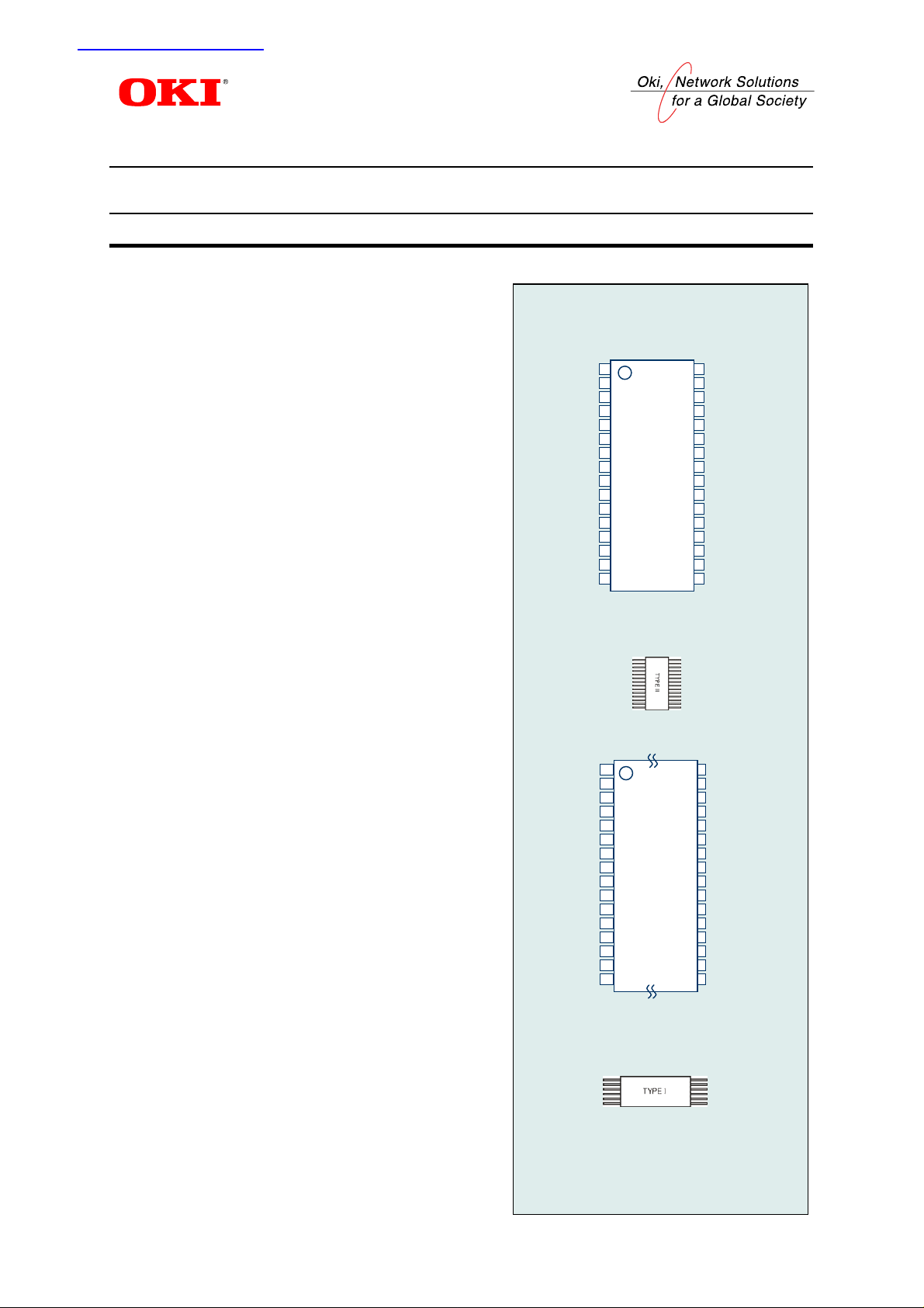
PACKAGES
· MR27T401E-xxxMA
32-pin plastic SOP (SOP32-P-525-1.27-K)
· MR27T401E-xxxTA
32-pin plastic TSOP (TSOP I 32-P-814-0.50-1K)
P2ROM ADVANCED TECHNOLOGY
P2ROM stands for Production Programmed ROM. This
exclusive Oki technology utilizes factory test equipment for
programming the customers c ode into the P2 ROM prior to fi nal
production testing. Advancements in this technology allows
production costs to be eq uivalent to M ASKROM and has many
advantages and added benefits over the other non-volatile
technologies, which include the following;
· Short lead time, since the P2ROM is programmed at the
final stage of the production process, a large P2ROM
inventory "bank system" of un-programmed packaged
products are maintained to provide an aggressive lead-time
and minimize liability as a custom product.
· No mask charge, since P2ROMs do not utilize a custom
mask for storing customer code, no mask charges apply.
· No additional programming charge, unlike Flash and
OTP that require additional programming and handling
costs, the P2ROM already has the code loaded at the
factory with minimal effect on the production throughput.
The cost is included in the unit price.
· Custom Marking is available at no additional charge.
PIN CONFIGURATION (TOP VIEW)
DC
1
A16
2
A15
3
A12
4
A7
5
A6
6
A5
7
A4
8
A3
9
A2
10
A1
11
A0
12
D0
13
D1
14
D2
15
VSS
16
32SOP,
A11
1
A9
2
A8
3
A13
4
A14
5
A17
6
A18
7
Vc
8
DC
9
A16
10
A15
11
A12
12
A7
13
A6
14
A5
15
A4
16
32TSOP(Type-I)
Vcc
32
18
31
17
30
14
29
13
28
8
27
9
26
11
25
OE#
24
10
23
CE#
22
D7
21
D6
20
D5
19
D4
18
D3
17
OE#
32
10
31
CE#
30
D7
29
D6
28
D5
27
D4
26
D3
25
Vss
24
D2
23
D1
22
D0
21
0
20
1
19
2
18
3
17
1/9

FEDR27T401E-02-01
OKI Semiconductor
BLOCK DIAGRAM
CE# OE#
CE OE
A0
A1
A2
A3
A4
A5
A6
A7
A8
A9
A10
A11
A12
A13
A14
A15
A16
A17
A18
Row Decoder
Address Buffer
Column Decoder
Memory Cell Matrix
512K × 8-Bit
Multiplexer
Output Buffer
D0 D1 D2 D3 D4 D5 D6 D7
PIN DESCRIPTIONS
Pin name Functions
A0 to A18 Address inputs
D0 to D7 Data outputs
CE# Chip enable input
OE# Output enable input
VCC Power supply voltage
VSS Ground
DC Don’t Care *,
* : Logical input level is ignored . However the pin is connected to internal circuit.
MR27T401E
2/9
FEDR27T401E-02-01
OKI Semiconductor
MR27T401E
FUNCTION TABLE
Mode CE# OE# VCC D0 to D7
Read L L Dout
Output disable L H Hi-Z
Standby H *
3.0 V
Hi-Z
∗: Don’t Care (H or L)
ABSOLUTE MAXIMUM RATINGS
Parameter Symbol Condition Value Unit
Operating temperature under bias Ta 0 to 70 °C
Storage temperature Tstg
Input voltage VI –0.5 to VCC+0.5 V
Output voltage VO –0.5 to VCC+0.5 V
Power supply voltage VCC
Power dissipation per package PD — 1.0 W
—
relative to V
SS
–55 to 125 °C
–0.5 to 5 V
RECOMMENDED OPERATING CONDITIONS
(Ta = 0 to 70°C)
Parameter Symbol Condition Min. Typ. Max. Unit
VCC power supply voltage VCC 2.7 — 3.6 V
= 2.7 to 3.6 V
Input “H” level VIH 2.2 — VCC+0.5∗ V
Input “L” level VIL
V
CC
–0.5∗∗ — 0.6 V
Voltage is relative to V
SS
.
∗ : Vcc+1.5V(Max.) when pulse width of overshoot is less than 10ns.
∗∗ : -1.5V(Min.) when pulse width of undershoot is less than 10ns.
PIN CAPACITANCE
(VCC = 3.0 V, Ta = 25°C, f = 1 MHz)
Parameter Symbol Condition Min. Typ. Max. Unit
Input C
DC C
Output C
— — 8
IN1
IN2
V
OUT
V
= 0 V
I
= 0 V — — 10
O
— — 200
pF
3/9
 Loading...