


OKI Semiconductor
FEDR27C1602B-01-03
Issue Date: Jun. 17, 2003
MR27C1602B
1,048,576–Word × 16–Bit or 2,097,152–Word × 8–Bit One Time PROM
GENERAL DESCRIPTION
The MR27C1602B is a 16 Mbit electrically One Time Programmable Read-Only Memory that can be electrically
switched between 1,048,576-word × 16-bit and 2,097,152-word × 8-bit by the state of the BYTE# pin. The
MR27C1602B supports high speed asynchronous read operation using a single 5.0V power supply.
FEATURES
· 1,048,576-word × 16-bit/2,097,152-word × 8-bit electrically switch able configuration
· +5.0 V power supply
· Access time 90 nS MAX
· Operating current 70 mA MAX
· Standby current 50 µA MAX
· Input/Output TTL compatible
· Tri-state output
· Packages:
42-pin plastic DIP (DIP42-P-600-2.54) (MR27C1602BRA)
44-pin plastic SOP (SOP44-P-600-1.27-K (MR27C1602BMA)
1/14
FEDR27C1602B-01-03
A
A
A
A
A
A
A
A
A
A
A
A
A
A
A
A
A
A
A
A
OKI Semiconductor
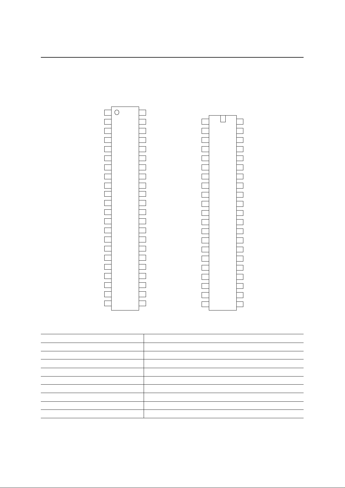
PIN CONFIGURATION (TOP VIEW)
Pin name Functions
D15/A–1 Data output/Address input
A0 to A19 Address input
D0 to D14 Data output
CE# Chip enable
OE# Output enable
BYTE#/VPP Mode switch/Program power supply voltage
VCC Power supply voltage
VSS GND
NC Non connection
NC
A18
A17
A7
A6
A5
A4
A3
A2
A1
A0
CE#
V
SS
OE#
D0
D8
D1
D9
D2
D10
D3
D11
1
2
3
4
5
6
7
8
9
10
11
12
13
14
15
16
17
18
19
20
21
22
44-pin SOP
44
43
42
41
40
39
38
37
36
35
34
33
32
31
30
29
28
27
26
25
24
23
NC
19
8
9
10
11
12
13
14
15
16
BYTE#/V
V
SS
D15/A–1
D7
D14
D6
D13
D5
D12
D4
V
CC
MR27C1602B (OTP)
A18
1
A17
2
3
A7
4
A6
5
A5
6
A4
7
A3
8
A2
9
A1
10
A0
11
CE#
PP
12
V
SS
13
OE#
14
D0
15
D8
16
D1
17
D9
18
D2
19
D10
20
D3
21
D11
42-pin DIP
42
41
40
39
38
37
36
35
34
33
BYTE#/V
32
VSS
31
D15/A–1
30
D7
29
D14
28
D6
27
D13
26
D5
25
D12
24
D4
23
V
22
19
8
9
10
11
12
13
14
15
16
CC
PP
2/14
FEDR27C1602B-01-03
A0
–
OKI Semiconductor
MR27C1602B (OTP)
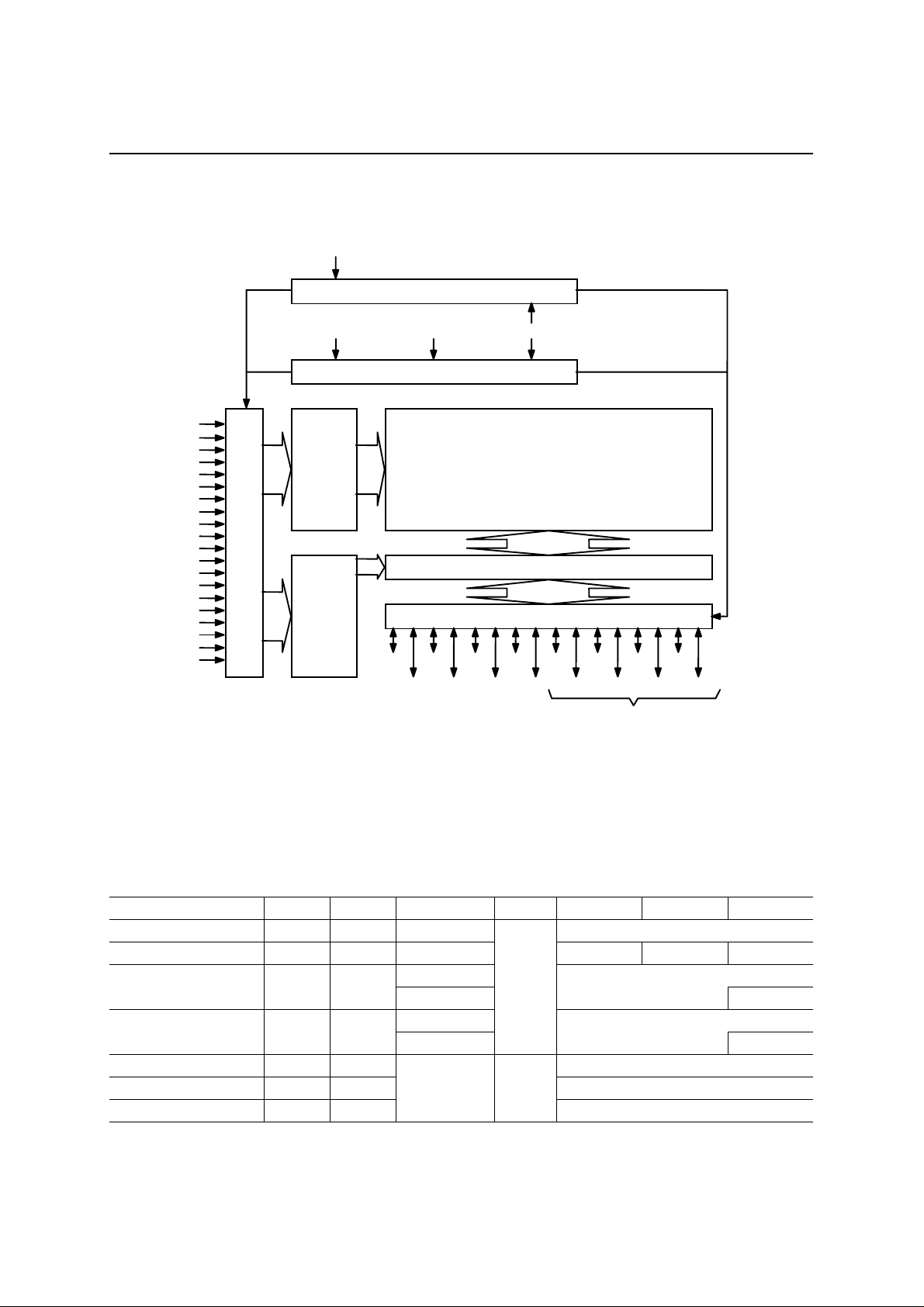
BLOCK DIAGRAM
A
1
× 8/× 16 Switch
CE# BYTE#/V
OE#
PP
CE PGM OE
A1
A2
A3
A4
A5
A6
A7
A8
A9
A10
A11
A12
A13
A14
A15
A16
A17
A18
A19
Memory Cell Matrix
Row Decoder
Address Buffer
Column Decoder
1,048,576 × 16-Bit or 2,097,152 × 8-Bit
Multiplexer
Output Buffer
D0 D2 D4 D6 D8 D10 D12 D14
D1 D3 D5 D7 D9 D11 D13 D15
In 8-bit output mode, these pins
are placed in a high-Z state and
pin D15 functions as the A-1
address pin.
FUNCTION TABLE
Mode CE# OE# BYTE#/VPP VCC D0 to D7 D8 to D14 D15/A–1
Read (16-Bit) L L H D
Read (8-Bit) L L L D
Output disable L H
Standby H ∗
Program L H DIN
Program inhibit H H Hi–Z
Program verify H L
H
L
H
L
9.75 V 4.0 V
5.0 V
∗: Don’t Care (H or L)
Hi–Z L/H
OUT
Hi–Z
Hi–Z
D
OUT
OUT
∗
∗
3/14
FEDR27C1602B-01-03
OKI Semiconductor
MR27C1602B (OTP)
ABSOLUTE MAXIMUM RATINGS
Parameter Symbol Condition Value Unit
Operating temperature under bias Ta 0 to 70 °C
Storage temperature Tstg
Input voltage VI –0.5 to VCC+0.5 V
Output voltage VO –0.5 to VCC+0.5 V
Power supply voltage VCC –0.5 to 7 V
Program power supply voltage VPP
Power dissipation per package PD — 1.0 W
—
relative to V
SS
–55 to 125 °C
–0.5 to 11.5 V
RECOMMENDED OPERATING CONDITIONS
(Ta = 0 to 70°C)
Parameter Symbol Condition Min. Typ. Max. Unit
VCC power supply voltage VCC 4.5 — 5.5 V
VPP power supply voltage VPP –0.5 — VCC+0.5 V
Input “H” level VIH 2.2 — VCC+0.5∗ V
Input “L” level VIL
Voltage is relative to V
SS
.
∗ : Vcc+1.5V(Max.) when pulse width of overshoot is less than 10ns.
∗∗ : -1.5V(Min.) when pulse width of undershoot is less than 10ns.
V
= 4.5 to 5.5 V
CC
–0.5∗∗ — 0.8 V
4/14
FEDR27C1602B-01-03
OKI Semiconductor
MR27C1602B (OTP)
ELECTRICAL CHARACTERISTICS
DC Characteristics
(VCC = 5.0 V ± 0.5 V, Ta = 0 to 70°C)
parameter Symbol Condition Min. Typ. Max. Unit
Input leakage current ILI V
Output leakage current ILO V
I
CE# = VCC — — 50 µA VCC power supply current
CCSC
(Standby)
V
power supply current
CC
(Read)
I
CE# = VIH — — 1 mΑ
CCST
I
CCA
VPP power supply current IPP V
Input “H” level VIH — 2.2 — VCC+0.5∗ V
Input “L” level VIL — –0.5∗∗ — 0.8 V
Output “H” level VOH I
Output “L” level VOL I
Voltage is relative to V
SS
.
∗ : Vcc+1.5V(Max.) when pulse width of overshoot is less than 10ns.
∗∗ : -1.5V(Min.) when pulse width of undershoot is less than 10ns.
AC Characteristics
Parameter Symbol Condition Min. Max. Unit
Address cycle time tC — 90 — ns
Address access time t
CE# = OE# = VIL — 90 ns
ACC
CE access time tCE OE# = VIL — 90 ns
OE access time tOE CE# = VIL — 45 ns
t
OE# = VIL 0 30 ns
Output disable time
CHZ
CE# = VIL 0 25 ns
t
OHZ
Output hold time tOH CE# = OE# = VIL 0 — ns
Measurement conditions
Input signal level--------------------------------0 V/3 V
Input timing reference level ------------------0.8 V/2.0 V
Output load---------------------------------------1TTL gate + 100 pF
Output timing reference level----------------0.8 V/2.0 V
= 0 to VCC — — 10 µA
I
= 0 to VCC — — 10 µA
O
CE# = V
, OE# = V
IL
tc = 90 ns
= VCC — — 10 µA
PP
= –400 µA 2.4 — — V
OH
= 2.1 mA — — 0.4 V
OL
IH
— — 70 mA
(VCC = 5.0 V ± 0.5 V, Ta = 0 to 70°C)
2.08 V
Output
800 Ω
100 pF
(Including scope and jig)
5/14

FEDR27C1602B-01-03
OKI Semiconductor
TIMING CHART (READ CYCLE)
16-Bit Read Mode (BYTE# = V
A0 to A19
CE#
OE#
t
D0 to D15
Hi-Z
8-Bit Read Mode (BYTE# = VIL)
A–1 to A19
CE#
MR27C1602B (OTP)
)
IH
t
t
t
t
t
t
t
Valid Data
t
t
t
t
Valid Data
Hi-Z
t
t
t
OE#
D0 to D7
D8 to D14
Hi-Z
t
t
t
Valid Data
t
Hi-Z
Valid Data
t
Hi-Z
6/14

FEDR27C1602B-01-03
OKI Semiconductor
MR27C1602B (OTP)
ELECTRICAL CHARACTERISTICS (PROGRAMMING OPERATION)
DC Characteristics
(Ta = 25°C ± 5°C)
Parameter Symbol Condition Min. Typ. Max. Unit
Input leakage current ILI V
VPP power supply current (Program) I
CE# = VIL — — 50 mA
PP2
VCC power supply current ICC — — — 70 mA
Input “H” level VIH — VCC+1.0 — VCC+0.5 V
Input “L” level VIL — –0.5 — 0.6 V
Output “H” level VOH IOH = –400 µA 2.4 — — V
Output “L” level VOL I
Program voltage VPP — 9.5 9.75 10.0 V
VCC power supply voltage (Program) VCC — 3.9 4.0 4.1 V
VCC power supply voltage (Verify-1) V
VCC power supply voltage (Verify-2) V
VCC power supply voltage (Verify-3) V
— 5.9 6.0 6.1 V
CV1
— 4.4 4.5 4.6 V
CV2
— 5.4 5.5 5.6 V
CV3
Voltage is relative to VSS.
AC Characteristics
(VCC = 4.0 V ± 0.1 V, BYTE#/VPP = 9.75 V ± 0.25 V, Ta = 25°C ± 5°C)
Parameter Symbol Condition Min. Typ. Max. Unit
Address set-up time tAS — 100 — — ns
OE set-up time t
OES
Data set-up time tDS — 100 — — ns
Address hold time tAH — 2 — — µs
Data hold time tDH — 100 — — ns
Output float delay time from OE t
V
voltage set-up time tVS — 2 — — µs
PP
OHZ
Program pulse width tPW — 9 10 11 µs
Data valid from OE t
Address hold from OE high t
OE
AOH
Pin Check Function
Pin Check Function is to check contact between each device-pin and each socket-lead with EPR OM programm er.
Setting up address as following condition call the preprogrammed codes on device outputs.
(VCC = 4.0 V ± 0.1 V, CE# = VIL, OE# = VIL, BYTE#/VPP = VIH, Ta = 25°C ± 5°C)
A0 A1 A2 A3 A4 A5 A6 A7 A8 A9 A10 A11 A12 A13 A14 A15 A16 A17 A18 A19 DATA
1 0 1 0 1 0 1 0 1 VH
0 1 0 1 0 1 0 1 0 VH
Other conditions FFFF
∗: VH = 8 V ± 0.25 V
= VCC+0.5 V — — 10 µA
I
= 2.1 mA — — 0.45 V
OL
— 2 — — µs
— 0 — 25 ns
— — — 50 ns
— 0 — — ns
∗
1 0 1 0 1 0 1 1 0 0 FF00
∗
0 1 0 1 0 1 0 0 1 1 00FF
7/14

FEDR27C1602B-01-03
OKI Semiconductor
Consecutive Programming Waveforms
A0 to A19
t
AS
CE#
OE#
D0 to D15
tVS
t
DS
BYTE#/Vpp
Consecutive Program Verify Waveforms
A0 to A19
t
PW
Din
MR27C1602B (OTP)
t
AH
High
tDH
Din
CE#
OE#
D0 to D15
BYTE#/Vpp
t
ACC
High
tOE
t
Dout
AHO
t
OHZ
Dout
9.75 V
8/14

FEDR27C1602B-01-03
OKI Semiconductor
MR27C1602B (OTP)
Program and Program Verify Cycle Waveforms
A0 to A19
t
AS
t
AHO
CE#
OE#
D0 to D15
t
OHZ
tDS
t
PW
Din
t
tDH
OES
t
OE
Dout
t
OHZ
BYTE#/Vpp
9.75 V
Pin Capacitance
(VCC = 5.0 V, Ta = 25°C, f = 1 MHz)
Parameter Symbol Condition Min. Typ. Max. Unit
Input C
BYTE#/VPP C
Output C
— — 8(10)
IN1
IN2
V
OUT
= 0 V
V
I
= 0 V — — 10(12)
O
— — 120
( ) : DIP only
pF
9/14

FEDR27C1602B-01-03
y
OKI Semiconductor
Programming/Verify Flow Chart
Programming
Bad Insertion
NG
Start
Pin Check
PASS
X=0
Address = First Location
= 4.0 V
V
CC
V
= 9.75 V
PP
Verif
Start
Pin Check
PASS
Address = First Location
VCC=4.5V/VPP =4.5V(V
Verify(All Address)
PASS
V
=5.5V/VPP=5.5V(V
CC
MR27C1602B (OTP)
NG
CV2
CV3
Bad Insertion
)
NG
)
Increment Address
NO
YES
Device Failed
X=X+1
X=2
Program 10 µs
NO
Last Address?
Address = First Location
VCC = 6V/VPP =6V(V
NG
Verify(All Address)
V
=4.5V/VPP =4.5V(V
CC
NG
Verify(All Address)
Device Passed
YES
PASS
PASS
CV1
)
CV2
Verify(All Address)
NG
PASS
Device Passed
Device Failed
)
10/14

FEDR27C1602B-01-03
OKI Semiconductor
PACKAGE DIMENSIONS
SOP44-P-600-1.27-K
Mirror finish
MR27C1602B (OTP)
(Unit: mm)
Package material Epoxy resin
Lead frame material 42 alloy
5
Pin treatment
Package weight (g) 2.10 TYP.
Rev. No./Last Revised 4/Dec. 5, 1996
Solder plating (≥5µm)
Notes for Mounting the Surface Mount Type Package
The surface mount type packages are very susceptible to heat in reflow mounting and humidity
absorbed in storage.
Therefore, before you perform reflow mounting, contact Oki’s responsible sales person for the product
name, package name, pin number, package code and desired mounting conditions (reflow method,
temperature and times).
11/14

FEDR27C1602B-01-03
OKI Semiconductor
DIP42-P-600-2.54
5
MR27C1602B (OTP)
(Unit: mm)
Package material Epoxy resin
Lead frame material 42 alloy
Pin treatment
Package weight (g) 6.20 TYP.
Rev. No./Last Revised 2/Dec. 11, 1996
Solder plating (≥5µm)
12/14

FEDR27C1602B-01-03
OKI Semiconductor
REVISION HISTORY
Edition
Page
Current
Edition
Description
Document
No.
FEDR27V1602B-01-01 Dec, 2001 – – Final edition 1
FEDR27V1602B-01-03 Jun. 17, 2003 – – Change over-bar fonts.
Date
Previous
MR27C1602B (OTP)
13/14

FEDR27C1602B-01-03
OKI Semiconductor
MR27C1602B (OTP)
NOTICE
1. The information contained herein can change without notice owing to product and/or technical improvements.
Before using the product, please make sure that the information being referred to is up-to-date.
2. The outline of action and examples for application circuits described herein have been chosen as an
explanation for the standard action an d performance of the product. When pl anning to use the pro duct, please
ensure that the external conditions are reflected in the actual circuit, assembly, and program designs.
3. When designing your product, please use our product below the specified maximum ratings and within the
specified operating ranges including, but not limited to, operating voltage, power dissipation, and operating
temperature.
4. Oki assumes no responsibility or liability whatsoever for any failure or unusual or unexpected operation
resulting from misuse, neglect, improper installation, repair, alteration or accident, improper handling, or
unusual physical or electrical stress including, but not limited to, expos ure to parameters beyo nd the specified
maximum ratings or operation outside the specified operating range.
5. Neither indemnity against nor license of a third party’s industrial and intellectual property right, etc. is
granted by us in connection wit h the use of the product and/or the i nformation and drawi ngs contained herein.
No responsibility is assumed by us for any infringement of a third party’s right which may result from the use
thereof.
6. The products listed in this document are intended for use in general electronics equipment for commercial
applications (e.g., office automation, communication equipment, measurement equipment, consumer
electronics, etc.). These products are not, unless specifically authorized by Oki, authorized for use in any
system or application that requires special or enhanced quality and reliability characteristics nor in any
system or application where the failure of such system or application may result in the loss or damage of
property, or death or injury to humans.
Such applications include, but are not limited to, traffic and automotive equipment, safety devices, aerospace
equipment, nuclear power control, medical equipment, and life-support systems.
7. Certain products in this document may need government approval before they can be exported to particular
countries. The purchaser assumes the responsibility of determining the leg ality of export of these products
and will take appropriate and necessary steps at their own expense for these.
8. No part of the contents contained herein may be reprinted or reproduced without our prior permission.
Copyright 2003 Oki Electric Industry Co., Lt d.
14/14
 Loading...