


PEDL60851C-02
1
Semiconductor
ML60851C
USB Device Controller
Preliminary
This version: Dec. 1999
GENERAL DESCRIPTION
The ML60851C is a general purpose Universal Serial Bus (USB) device controller. The ML60851C provides a
USB interface, control/status block, application interface, and FIFOs. The FIFO interface and two types of
transfer have been optimized for BulkOut devices such as printers and BulkIn devices such as digital still cameras
and image scanners. In addition, Mass Storage devices are also applicable to this device.
FEATURES
•
USB 1.0 compliant
•
Built-in USB transceiver circuit
•
Full-speed (12 Mb/sec) support
•
Supports printer device class, image device class, and Mass Storage device class
•
Supports three types of transfer; control transfer, bulk transfer, and interrupt transfer
•
Built-in FIFOs for control transfer
Two 8-byte FIFOs (one for receive FIFO and the other for transmit FIFO)
•
Built-in FIFOs for bulk transfer (available for either receive FIFO or transmit FIFO)
One 64-byte FIFO
Two 64-byte FIFOs
•
Built-in FIFO for interrupt transfer
One 8-byte FIFO
•
Supports one control endpoint, two bulk endpoint addresses, and one interrupt endpoint address
•
Two 64-byte FIFOs enable fast BulkOut transfer and BulkIn transfer
•
Supports 8 bit/16 bit DMA transfer
•
V
is 3.0 V to 3.6 V
CC
•
Supporting dual power supply enables 5 V application interface
•
Built-in 48 MHz oscillator circuit
•
Package options:
44-pin plastic QFP (QFP44-P-910-0.80-2K) (Product name: ML60851CGA)
44-pin plastic TQFP (TQFP44-P-1010-0.80-K) (Product name: ML60851CTB)
1/67

1
Semiconductor
BLOCK DIAGRAM
Application
Module
(Local MCU)
PEDL60851C-02
ML60851C
A7:A0
ML60851C
D15:D0
Application
Status/Control
DPLL
, ,
Interface
Protocol
Engine
DACK
Endpoint FIFO/
8-byte Setup Register
XIN
Oscillator
XOUT
48 MHz
D+
USB
Transceiver
D-
USB Bus
2/67

1
Semiconductor
PIN CONFIGURATION (TOP VIEW)
PEDL60851C-02
ML60851C
D+
D-
V
CC3
TEST1
TEST2
XIN
XOUT
CS
RD
WR
RESET
CC5
GND
V
AD3
AD2
AD1
AD0
4443424140393837363534
1
2
3
4
5
6
7
8
9
10
11
1213141516171819202122
D15
D14
D13
D12
INTR
GND
44-Pin Plastic QFP
AD4
CC5
V
AD5
D11
AD6
D10
AD7
D9
DREQ
D8
33
DACK
32
A0
31
A1
30
A2
29
A3
28
A4
27
A5
26
A6
25
A7
24
ADSEL
23
ALE
D+
D-
V
CC3
TEST1
TEST2
XIN
XOUT
CS
RD
WR
RESET
CC5
AD3
AD2
AD1
AD0
44
43
42
41
40
1
2
3
4
5
6
7
8
9
10
11
12
13
14
15
16
D15
D14
D13
INTR
D12
AD5
AD4
VSSV
39
38
37
17
18
19
SS
CC5
V
D11
V
AD6
36
20
D10
AD7
35
21
D9
DREQ
34
22
D8
33
DACK
32
A0
31
A1
30
A2
29
A3
28
A4
27
A5
26
A6
25
A7
24
ADSEL
23
ALE
44-Pin Plastic TQFP
3/67

PEDL60851C-02
1
Semiconductor
PIN DESCRIPTION
Pin Symbol Type Description
1,2 D+, D- I/O USB data
6, 7 XIN, XOUT — Pins for external crystal oscillator
4, 5 TEST14, 2 I Test pins (normally “L”)
13 to 16,
19 to 22
35 to 38,
41 to 44
25 to 32 A7 to A0 I Address inputs
8
9
10
12
34
33 DACK I DMA acknowledge signal input pin
23 ALE I Address latch enable signal input pin
24 ADSEL I Address input mode select input pin. “H”: address/data multiplex
11
D15 to D18 I/O
AD7 to AD0 I/O
CS
RD
WR
INTR
DREQ
RESET
O
O
I
I
I
I
Data bus (MSB)
Data bus (LSB)/address inputs
Chip select signal input pin. LOW active
Read signal input pin. LOW active
Write signal input pin. LOW active
Interrupt request signal output pin
DMA request output pin
System reset signal input pin. LOW active.
ML60851C
4/67

1
Semiconductor
INTERNAL REGISTERS
Addresses and Names of Registers
Addresses Register Page
A5:A0
00h 01b —
01h 01b —
02h 01b — EP2RXFIFO Endpoint 2 Receive FIFO Data
03h 01b — Reserved
00h — 11b
01h — 11b
02h — 11b
03h — 11b
Read
A7, A6
Write
A7, A6
Symbol Register name
EP0RXFIFO Endpoint 0 Receive FIFO Data
EP1RXFIFO Endpoint 1 Receive FIFO Data
EP0TXFIFO Endpoint 0 Transmit FIFO Data
EP1TXFIFO Endpoint 1 Transmit FIFO Data
EP2TXFIFO Endpoint 2 Transmit FIFO Data
EP3TXFIFO Endpoint 3 Transmit FIFO Data
PEDL60851C-02
ML60851C
7
7
8
9
9
10
10
00h 11b 01b DVCADR Device Address Register
01h 11b 01b
02h 11b —
03h 11b —
04h 11b —
08h 11b 01b PKTRDY Endpoint Packet-Ready Register
09h 11b — EP0RXCNT Endpoint 0 Receive-Byte Count Register
0Ah 11b —
0Bh 11b —
0Ch 11b —
0Dh 11b —
0Eh — 01b CLRFIFO Transmit FIFO Clear Register
0Fh — 01b SYSCON System Control Register
10h 11b —
11h 11b —
12h 11b —
13h 11b —
14h 11b — wIndexLSB wIndexLSB Setup Register
15h 11b — wIndexMSB wIndexMSB Setup Register
16h 11b —
17h 11b —
1Ah 11b 01b
1Bh 11b 01b
1Ch 11b — INTSTAT Interrupt Status Register
1Dh 11b 01b DMACON DMA Control Register
1Eh 11b 01b
1Fh — —
DVCSTAT Device Status Register
PKTERR Packet Error Register
FIFOSTAT1 FIFO Status Register 1
FIFOSTAT2 FIFO Status Register 2
EP1RXCNT Endpoint 1 Receive-Byte Count Register
EP2RXCNT Endpoint 2 Receive-Byte Count Register
Reserved
REVISION Revision Register
bmRequestType bmRequestType Setup Register
bRequest bRequest Setup Register
wValueLSB wValueLSB Setup Register
wValueMSB wValueMSB Setup Register
wLengthLSB wLengthLSB Setup Register
wLengthMSB wLengthMSB Setup Register
POLSEL Assertion Select Register
INTENBL Interrupt Enable Register
DMAINTVL DMA Interval Register
Reserved
11
11
13
13
14
15
19
19
20
21
21
22
23
23
24
24
24
24
25
25
26
27
28
30
31
5/67

PEDL60851C-02
1
Semiconductor
ML60851C
Addresses and Names of Registers (Continued)
Addresses Symbol Register name Page
20h 11b — EP0RXCON Endpoint 0 Receive Control Register 32
21h 11b — EP0RXTGL Endpoint 0 Receive Data Toggle Register 32
22h 11b 01b EP0RXPLD Endpoint 0 Receive Payload Register 33
23h — — Reserved
24h 11b 01b EP1CON Endpoint 1 Control Register 34
25h 11b 01b EP1TGL Endpoint 1 Data Toggle Register 35
26h 11b 01b EP1PLD Endpoint 1 Payload Register 35
27h — — Reserved
28h — — Reserved
29h — — Reserved
2Ah — — Reserved
2Bh — — Reserved
2Ch — — Reserved
2Dh — — Reserved
2Eh — — Reserved
2Fh — — Reserved
30h 11b — EP0TXCON Endpoint 0 Transmit Control Register 36
31h 11b — EP0TXTGL Endpoint 0 Transmit Data Toggle Register 36
32h 11b 01b EP0TXPLD Endpoint 0 Transmit Payload Register 37
33h 11b 01b EP0STAT Endpoint 0 Status Register 38
34h 11b 01b EP2CON Endpoint 2 Control Register 40
35h 11b 01b EP2TGL Endpoint 2 Data Toggle Register 41
36h 11b 01b EP2PLD Endpoint 2 Payload Register 41
37h — — Reserved
38h 11b 01b EP3CON Endpoint 3 Control Register 42
39h 11b 01b EP3TGL Endpoint 3 Data Toggle Register 43
3Ah 11b 01b EP3PLD Endpoint 3 Payload Register 43
3Bh — — Reserved
3Ch — — Reserved
3Dh — — Reserved
3Eh — — Reserved
3Fh — — Reserved
6/67

PEDL60851C-02
1
Semiconductor
ML60851C
FUNCTIONS OF REGISTERS
End Point 0 Receive FIFO (EP0RXFIFO)
Read address 40h
Write address -
D7 D6 D5 D4 D3 D2 D1 D0
After a hardware resetxxxxxxxx
After a bus reset xxxxxxxx
Definition EP0 Receive data (R)
The receive data from the host computer in the data state during a control Write transfer is stored in EP0RXFIFO.
The EP0 receive data can be read out by the local MPU through reading the address 40h when the ML60851C
issues an EP0 receive packet ready interrupt request. It is possible to read successively the data in the packet by
reading cont inuousl y.
The EP2RXFIFO is cleared under the following conditions:
1. When the local MPU resets the EP0 receive packet ready bit (A “1” is written in PKTRDY(0)).
2. When a setup packet is received.
3. When the local MCU writes a “0” in the stall bit (EP0STAT(2)).
End Point 1 Receive FIFO (EP1RXFIFO)
Read address 41h
Write address —
D7 D6 D5 D4 D3 D2 D1 D0
After a hardware resetxxxxxxxx
After a bus reset xxxxxxxx
Definition EP1 Receive data (R)
It is possible to read out the EP1 receive data by reading the address 41h. When EP1 is set for bulk reception
(BULK OUT), The local MCU should read EP1RXFIFO when the ML60851C issues an EP2 packet ready
interrupt request. It is possible to read successively th e data in the packet by readin g continuously. When the data
transfer direction of EP1 is set as “Transmit”, all accesses to this address will be invalid.
The EP1RXFIFO is cleared under the following conditions:
1. When an OUT token is received for EP1.
2. When the EP1 receive packet ready bit is reset. (A “1” is written in PKTRDY(1).)
3. When the local MCU writes a “0” in the stall bit (EP1CON(1)).
Even when a DMA read with a 16-bit width is made from EP1RXFIFO, the address is A7:A0 = 41h.
7/67

PEDL60851C-02
1
Semiconductor
ML60851C
End Point 2 Receive FIFO (EP2RXFIFO)
Read address 42h
Write address
D7 D6 D5 D4 D3 D2 D1 D0
After a hardware resetxxxxxxxx
After a bus reset xxxxxxxx
Definition EP2 Receive data (R)
—
It is possible to read out the EP2 receive data by reading the address 42h. When EP2 is set for bulk reception (Bulk
OUT), the local MCU should read EP2R XFIFO when the ML 60851C issues an EP2 packet ready int errupt request.
It is possible to read successively the data in the packet by reading con t inuously. When th e data transfer direction
of EP2 is set as ‘Transmit’, all accesses to this address will be invalid.
The EP2RXFIFO is cleared under the following conditions:
1. When an OUT token is received for EP2.
2. When the EP2 receive packet ready bit is reset. (A “1” is written in PKTRDY(2).)
3. When the local MCU writes a “0” in the stall bit (EP2CON(1)).
8/67

PEDL60851C-02
1
Semiconductor
ML60851C
End Point 0 Transmit FIFO (EP0TXFIFO)
Read address —
Write address C0h
D7 D6 D5 D4 D3 D2 D1 D0
After a hardware resetxxxxxxxx
After a bus reset xxxxxxxx
Definition EP0 Transmit data (W)
The EP0 transmit data can be written in by writing to the address C0h. The receive data from the host in the data
stage during a control read transfer is stored in EP0TXFIFO . When the ML60851C issues an EP0 transm it pack et
ready interrupt request, the local MC U writes the transmit data to the addres s C0h. It is possible to write the packet
data successively by writing continuously.
The EP0 TXFIFO is cleared under the following conditions:
1. When an ACK is received from the host for the data transmission from EP0.
2. When a setup packet is received.
End Point 1 Transmit FIFO (EP1TXFIFO)
Read address
Write address C1h
D7 D6 D5 D4 D3 D2 D1 D0
After a hardware resetxxxxxxxx
After a bus reset xxxxxxxx
Definition EP1 Transmit data (W)
—
The EP1 transmit data can be written in by writing to the address C1h. When EP1 has been set for bulk
transmission (BULK IN), The local MCU should write the transmit data in EP1TXFIFO when the ML60851C
issues an EP1 packet ready interrupt request. It is possible to write the packet data successively by writing
continuously. When the data transfer direction of EP 1 is set as ‘Receive’, all accesses to this add ress will be
invalid.
The EP1 transmit FIFO is cleared under the following conditions:
1. When an ACK is received from the host for the data transmission from EP1.
2. When the local MCU writes a “1” in the EP1FIFO clear bit (CLRFIFO(1)).
Even when a DMA write with a 16-bit width is made in EP1TXFIFO, the address is A7:A0 = 41h.
9/67

PEDL60851C-02
1
Semiconductor
ML60851C
End Point 2 Transmit FIFO (EP2TXFIFO)
Read address —
Write address C2h
D7 D6 D5 D4 D3 D2 D1 D0
After a hardware resetxxxxxxxx
After a bus reset xxxxxxxx
Definition EP2 Transmit data (W)
The EP2 transmit data can be written in by writing to the address C2h. When EP2 has been set for bulk
transmission (BULK IN), The local MCU should write the transmit data in EP1TXFIFO when the ML60851C
issues an EP2 packet ready interrupt request. It is possible to write the packet data successively by writing
continuously. When the data transfer direction of EP2 is set as “Receive”, all accesses to this address will be
invalid.
The EP2 TXFIFO is cleared under the following conditions:
1. When an ACK is received from the host for the data transmission from EP2.
2. When the local MCU writes a “1” in the EP2FIFO clear bit (CLRFIFO(2)).
End Point 3 Transmit FIFO (EP3TXFIFO)
Read address —
Write address C3h
D7 D6 D5 D4 D3 D2 D1 D0
After a hardware resetxxxxxxxx
After a bus reset xxxxxxxx
Definition EP3 Transmit data (W)
The EP3 transmit data can be written in by writing to the address C3h. Make the local MCU write the transmit data
in EP3TXFIFO when the ML60851C issues an EP3 packet ready interrupt request. It is possible to write the
packet data successivel y by writing continuously.
The EP3 TXFIFO is cleared under the following conditions:
1. When an ACK is received from the host for the data transmission from EP3.
2. When the local MCU writes a “1” in the EP3FIFO clear bit (CLRFIFO(3)).
10/67

PEDL60851C-02
1
Semiconductor
ML60851C
Device Address Register (DVCADR)
Read address C0h
Write address 40h
D7 D6 D5 D4 D3 D2 D1 D0
After a hardware reset00000000
After a bus reset 00000000
Definition Device address (R/W)
The local MCU writes in this register the device address given by the SET_ADDRESS command from the host.
Thereafter, the ML60851C responds only to the token specifying this address among all the tokens from the host
computer. The default value is the address D6:D0 = 00h.
Note 1: It is possible to carry out addr es s ing usin g a 7- bit ad dr ess because up to 127 devices can be
connected according to the USB standard.
Note 2: The bit D7 is fixed at “0”, and even if a “1” is written in the bit D7, it will be invalid.
Device State Register (DVCSTAT)
Read address C1h
Write address 41h
D7 D6 D5 D4 D3 D2 D1 D0
After a hardware reset00000001
After a bus reset 00000001
Definition 0 0
Default state (R/W)
Address state (R/W)
Configuration state (R/W)
Suspend state (R)
Remote wake-up (R/W)
USB bus reset status clear (W)
This is a register for displaying the status of the device. The functions of the different bits are described below:
The bits D7 and D6 are fixed at “0” and even if a “1” is written in these bits, the write operation will be invalid.
Default state:
This bit is asserted in the initial state. The default state is valid from the time the power is switched ON and
the hardware resetting is complete. There is no need to write a “0” in this bit.
Address state:
When a SET_ADDRESS request arrives, the local MCU writes the device address in the device address
register. If necessary, by writing a “1” in this bit also at that time, it is possible to give an indication that the
ML60851C has entered the address state. Since the content of this bit does not affect the operation of the
ML60851C, there is no need to write in this bit if it will not be read out.
11/67

1
Semiconductor
Configuration state:
When the local MPU asserts the configuration bits EP1CON, EP2CON, or EP3CON in response to a
SET_CONFIGURATION request from the host computer when this IC is in the address state, by writing a
“1” in this bit also, if necessary, at that time, it is possible to give an indication that the ML60851C has
entered the configuration st ate. Since the con tent of this bit does n ot affect th e operation of the ML60851C,
there is no need to write in this bit if it will not be read out.
Remarks:
When all these three states are “1”, it m eans that this IC is normally operating. How ever, since these bits do
not affect the operation of the ML60851C, there is no n eed to write in these bits if they will not be read out.
Suspend state:
When the idle condition continues for more than 3ms in the USB bus, the ML60851C au tomatically asserts
this bit thereby indicating that it is going into the suspend state. At the same time, bit D6 of the interrupt
status register INTSTAT is asserted and the
INTR
pin is asserted. With this, the local MCU can suppress
the current consumption.
This bit is deasserted when the EOP of any type of packet is received.
Remote wake-up:
The ML60851C is in the suspend state, the remote wake-up function is activated when the local MCU
asserts this bit. When this bit is written while 5ms have not yet elapsed in the idle condit ion, the remote
wake-up signal is output after waiting for the idle condition to continue for the full 5ms period. Further,
when this bit is written after the idle condition has persisted for 5ms or more, the remote wake-up signal is
output immediately after this bit is written. This bit is deasserted auto matically when the suspe nd state is
released by receiving the resume instruction over the USB bus.
PEDL60851C-02
ML60851C
USB bus reset status clear:
When the ML60851C is in the USB bu s reset interru pt state (bit D5 of the interrupt statu s register, that is the
USB bus reset interrupt status bit is “1” and the
INTR
pin is asserted), it is possible to clear the interrupt
status by writing a “1” in this bit. (This makes the USB bus reset interrupt status bit “0” and deassertes
INTR
.) Although this bit can be read out, the read out value will always be “0”.
12/67

PEDL60851C-02
1
Semiconductor
ML60851C
Packet Error Register (PKTERR)
Read address C2h
Write address —
D7 D6 D5 D4 D3 D2 D1 D0
After a hardware reset00000000
After a bus reset 00000000
Definition 0 0
00
Bit stuff error (R)
Data CRC error (R)
Address CRC error (R)
PID Error (R)
Each bit is asserted when the corresponding error occurs and is deasserted when SOP is received.
This register is used to report the error information. This register is useful for the tests during development, or for
preparing the error frequency measurement report. This register is n ot particularly required f or the specification of
commercial a product.
FIFO Status Register 1 (FIFOSTAT1)
Read address C3h
Write address —
D7 D6 D5 D4 D3 D2 D1 D0
After a hardware reset00001010
After a bus reset 00001010
Definition 0 0
00
Receive FIFO0 Full (R)
Receive FIFO0 Empty (R)
FIFO1 Full (R)
FIFO1 Empty (R)
This register reports the statuses of the EP0RXFIFO and the FIFO for EP1. N orm ally, there is n o need to read this
register because it is sufficient to read the packet ready status before reading out or writing in a FIFO.
Receive FIFO0 Full: This bit becomes “1” when 8-bytes of data are stored in the EP0RXFIFO. This bit is
not set to “1” when a packet less than 8 bytes long (a short packet) is stored in.
Receive FIFO0 Empty: This bit will be “1” when the EP0RXFIFO0 is empty.
FIFO1 Full: This bit becomes “1” when 64 bytes of data is stored in the FIFO for EP1. This is true
during both transmission and reception. This bit does not become “1” in the case of a
short packet. The FIFO for EP1 has a two-layer structure and can store up to 128
bytes of data. This bit indicates the status of the FIFO in which data being written at
that time. In other words, this bit indicates the status of the FIFO into which the host
computer is writing data when EP1 is receiving data, and of the FIFO into which the
local MCU is writing data when EP1 is transmitting data.
FIFO1 Empty: This bit becomes “1” when the FIFO for EP1 is empty. This is true during both
transmission and reception. The FIFO for EP1 has a tw o-layer s tructure and can s tore
up to 128 bytes of data. This bit indicates the status of the FIFO which is being read
out at that time.
13/67

1
Semiconductor
FIFO0 Status Register 2 (FIFOSTAT2)
Read address C4h
Write address —
D7 D6 D5 D4 D3 D2 D1 D0
After a hardware reset00101010
After a bus reset 00101010
Definition 0 0
PEDL60851C-02
ML60851C
Transmit FIFO0 Full (R)
Transmit FIFO0 Empty (R)
FIFO2 Full (R)
FIFO2 Empty (R)
FIFO3 Full (R)
FIFO3 Empty (R)
This register reports the statuses of the EP0TXFIFO, the FIFO for EP2, and the FIFO for EP3. Normally, there is
no need to read this register because it is sufficient to read the packet ready status before reading out or writing in
a FIFO.
Transmit FIFO0 Full: This bit becomes “1” when 8-bytes o f data is stored in the EP0TXFIFO. T his bit is
not set to “1” when a packet less than 8 bytes (a short packet) is written in.
Transmit FIFO0 Empty: This bit will be “1” when the EP0 transmit FIFO0 is empty.
FIFO2 Full: This bit becomes “1” when 64 bytes of data is either stored or written in the FIFO for
EP2. This bit does not become “1” in the case of a short packet.
FIFO2 Empty: This bit becomes “1” when the FIFO of EP2 is empty.
FIFO3 Full: This bit becomes “1” when 64 bytes are written in the FIFO for EP3. This bit does not
become “1” in the case of a short packet.
FIFO3 Empty: This bit becomes “1” when the FIFO for EP3 is empty.
14/67

PEDL60851C-02
1
Semiconductor
ML60851C
End Point Packet Ready Register (PKTRDY)
This register indicates whether or not the preparations for reading out or writing in a packet data have been
completed. In addition, this register is also used for controlling the handshake packet (ACK/NAK)
Read address C8h
Write address 48h
D7 D6 D5 D4 D3 D2 D1 D0
After a hardware reset00000000
After a bus reset 00000000
Definition 0
EP0 Receive packet ready (R/Reset )
EP1 Receive packet ready (R/Reset )
EP2 Receive packet ready (R/Reset )
EP0 Transmit packet ready (R/Set)
EP1 Transmit packet ready (R/Set)
EP2 Transmit packet ready (R/Set)
EP3 Transmit packet ready (R/Set)
This is the register for indicating that the local MCU can request a read/write of the FIFO for each EP. The logical
sums (AND) of each of these bits and the corresponding bits of INTENBL become the bits of INTSTAT.
The ML60851C asserts a receive packet ready bit (set to “0”) and generates an interrupt cause. The local MCU
resets the receive packet ready bit after completion of the interrupt servicing (such as taking out data from the
corresponding receive FIFO, etc.,).
The ML60851C deasserts a transmit packet ready bit and generates an interrupt cause. The local MCU sets the
receive packet ready bit after completion of the interrupt servicing (such as writing data in the corresponding
transmit FIFO, etc.,).
The bit D3 is fixed at “0”, and even if a “1” is written in this bit, that write operation will be invalid.
The operations of the different bits of PKTRDY are described in detail below.
15/67

PEDL60851C-02
1
Semiconductor
EP0 Receive packet ready bit (D0)
This bit can be read by the local MCU. Further, this bit can be set to “0” by writing “1” to the D0 bit.
The conditions of asserting and deasserting this bit are the following.
Bit name Asserting condition Action when asserted
EP0 Receive packet ready (D0)
1. When data is received in EP0
and storing of one packet of
receive data in EP0RXFIFO is
completed.
2. When a setup packet is received
during a control Re ad or a contr ol
Write transfer.
EP0 is locked (that is, an NAK is
returned automatically when a data
packet is received from the host
computer).
(In the case of the asserting
condition 1, the local MCU can read
EP0RXFIFO.)
Bit name Deasserting condition Action when deasserted
EP0 Receive packet ready (D0)
1. When the local MCU resets
(writes a “1” in) this bit.
2. When the local MCU resets the
setup ready bit during a control
Write transfer.
Reception is possible in EP0.
ML60851C
R/Reset: Reading possible/ Reset when a “1” is written
R/Set: Reading possible/ Set when a “1” is written
16/67

PEDL60851C-02
1
Semiconductor
ML60851C
EP1 Receive Packet Ready Bit (D1)
This bit can be read by the local MCU. Further, this bit can be set to “0” by writing “1” to the D1 bit.
The conditions of asserting and deasserting this bit are the following. EP1 has a two-layer FIFO, and even the
packet ready bits are present independently for layer A and layer B. The switching between these two layers is
done automatically by the ML60851C.
Bit name Asserting condition Action when asserted
EP1 Receive packet ready (D1)
When an error-free packet is
received in either layer A or layer B.
The local MCU can read the
EP1RXFIFO. EP1 is locked when
both layer A and layer B have
received a packet data.
Bit name Deasserting condition Action when deasserted
EP1 Receive packet ready (D1) When the local MCU resets (writes a
“1”) in the bits of both layer A and
layer B.
Reception is possible in EP1 w hen at
least one of the bits of layer A and
layer B has been reset.
See the explanation of the operation of the two-layer FIFO given in the Section on ‘Functional Description’.
EP2 Receive Packet Ready Bit (D2)
This bit can be read by the local MCU. Further, this bit can be set to “0” by writing “1” to the D2 bit.
The conditions of asserting and deasserting this bit are the following.
Bit name Asserting condition Action when asserted
EP2 Receive packet ready (D2) When an error-free packet is
received.
EP2 is locked.
Bit name Deasserting condition Action when deasserted
EP2 Receive packet ready (D2) When the local MCU resets (writes a
“1” in) this bit.
Data reception is possible in EP2.
EP0 Transmit Packet Ready Bit (D4)
This bit can be read by the local MCU. Further, this bit can be set to “1” by writing “1” to the D4 bit.
The conditions of asserting and deasserting this bit are the following.
Bit name Asserting condition Action when asserted
EP0 Transmit packet ready (D4) When the local MCU sets this bit. Data transmission is possible from
EP0.
Bit name Deasserting condition Action when deasserted
EP0 Transmit packet ready (D4)
1. When an ACK is receiv ed from the
host computer in response to the
data transmission from EP0.
2. When a setup packet is received.
EP0 is locked. In other words, an
NAK is returned automatically when
an IN token is received from the host
computer.
17/67

PEDL60851C-02
1
Semiconductor
ML60851C
EP1 Transmit Packet Ready Bit (D5)
This bit can be read by the local MCU. Further, this bit can be set to “1” by writing “1” to the D5 bit.
The conditions of asserting and deasserting this bit are the following. EP1 has a two-layer FIFO, and even the
packet ready bits are present independently for layer A and layer B. The switching between these two layers is
performed automatically by the ML60851C.
Bit name Asserting condition Action when asserted
EP1 Transmit packet ready (D5)
When the local MCU has set the bits
of both layer A and layer B.
Data transmission is possible from
EP1 when the bit for at least one of
layer A and layer B has been
asserted.
Bit name Deasserting condition Action when deasserted
EP1 Transmit packet ready (D5) When an ACK is received from the
host computer for the data
transmission from either layer A or
layer B.
EP1 is locked when both layer A and
layer B have not prepared the
transmit data.
See the explanation of the operation of the two-layer FIFO given in the Section on ‘Functional Description’.
EP2 Transmit Packet Ready Bit (D6)
This bit can be read by the local MCU. Further, this bit can be set to “1” by writing “1” to the D6 bit.
The conditions of asserting and negating this bit are the following.
Bit name Asserting condition Action when asserted
EP2 Transmit packet ready (D6) When the local MCU has set this bit. Data transmission is possible from
EP2.
Bit name Deasserting condition Action when deasserted
EP2 Transmit packet ready (D6)
When an ACK is received from the
host computer in response to the
data transmission from EP2.
EP2 is locked.
EP3 Transmit Packet Ready Bit (D7)
This bit can be read by the local MCU. Further, this bit can be set to “1” by writing “1” to the D7 bit.
The conditions of asserting and deasserting this bit are the following.
Bit name Asserting condition Action when asserted
EP3 Transmit packet ready (D7) When the local MCU has set this bit. Data transmission is possible from
EP3.
Bit name Deasserting condition Action when deasserted
EP2 Transmit packet ready (D7) When an ACK is received from the
host computer in response to the
data transmission from EP3.
EP3 is locked.
18/67

PEDL60851C-02
1
Semiconductor
ML60851C
End Point 0 Receive Byte Count Register (EP0RXCNT)
Read address C9h
Write address —
D7 D6 D5 D4 D3 D2 D1 D0
After a hardware reset00000000
After a bus reset 00000000
Definition 0 Byte count of EP0 (R)
The ML60851C automatically counts the number of bytes in the packet being received by EP0 an d stored it in this
register. Although the coun t ing is performed up to the maxim um pack et si ze ente red i n th e payl oad reg i s ter in the
case of a full packet, the count will be less than this value in t he case o f a short p acket. The local MCU refers to
this value and reads the data of one packet from the EP0RXFIFO.
The EP0 receive byte count register is cleared under the following conditions:
1. When the local MCU resets the EP0 receive packet ready bit (by writing a “1” in PKTRDY(0)).
2. When a setup packet is received.
3. When the local MCU writes a “0” in the stall bit (EP0STAT(2)).
End Point 1 Receive Byte Count Register (EP1RXCNT)
Read address CAh
Write address —
D7 D6 D5 D4 D3 D2 D1 D0
After a hardware reset00000000
After a bus reset 00000000
Definition 0 Byte count of EP1 (R)
The ML60851C automatically counts the number of bytes in the packet being received by EP1 an d stored it in this
register. Although the coun t ing is performed up to the maxim um pack et si ze ente red i n th e payl oad reg i s ter in the
case of a full packet, the count will be less than this value in t he case o f a short p acket. The local MCU refers to
this value and reads the data of one packet from the EP1 receive FIFO.
This register is invalid when the EP1 transfer direction is set as ‘Transmit’.
The EP1 receive byte count register is cleared under the following conditions:
1. When an OUT token is received for EP1.
2. When the EP1 receive packet ready bit is reset (by writing a “1” in PKTRDY(1)).
3. When the local MCU writes a “0” in the stall bit (EP1CON(1)).
19/67

PEDL60851C-02
1
Semiconductor
ML60851C
End Point 2 Receive Byte Count Register (EP2RXCNT)
Read address CBh
Write address —
D7 D6 D5 D4 D3 D2 D1 D0
After a hardware reset00000000
After a bus reset 00000000
Definition 0 Byte Count of EP2 (R)
The ML60851C automatically counts the number of bytes in the packet being received by EP2 an d stored it in this
register. Although the coun t ing is performed up to the maxim um pack et si ze ente red i n th e payl oad reg i s ter in the
case of a full packet, the count will be less than this value in the case o f a short packet. T he local MCU refers to
this value and reads the data of one packet from the EP2RXFIFO.
This register is invalid when the EP2 transfer direction is set as ‘Transmit’.
The EP2 receive byte count register is cleared under the following conditions:
1. When an OUT token is received for EP2.
2. When the EP2 receive packet ready bit is reset (by writing a “1” in PKTRDY(2)).
3. When the local MCU writes a “0” in the stall bit (EP2CON(1)).
20/67

1
Semiconductor
Revision Register (REVISION)
Read address CDh
Write address —
D7 D6 D5 D4 D3 D2 D1 D0
After a hardware reset
After a bus reset
Definition
Revision No. of Chip
Transmit FIFO Clear Register (CLRFIFO)
Read address —
Write address 4Eh
D7 D6 D5 D4 D3 D2 D1 D0
After a hardware reset
After a bus reset
Definition 0 0 0 0
Cannot be read (indeterminate)
Cannot be read (indeterminate)
PEDL60851C-02
ML60851C
EP1 Transmit FIFO Clear
EP2 Transmit FIFO Clear
EP3 Transmit FIFO Clear
EP1 to EP3 FIFO Clear: When each EP has been set for transmission, by writing a “1” in these bits, the
corresponding FIFOs are cleared at the Write pulse and also the corresponding EP
Packet Ready bits are reset.
21/67

PEDL60851C-02
1
Semiconductor
ML60851C
System Control Register (SYSCON)
Read address —
Write address 4Fh
D7 D6 D5 D4 D3 D2 D1 D0
After a hardware reset
After a bus reset
Definition 0 0 0
Cannot be read (indeterminate)
Cannot be read (indeterminate)
Software Reset
Oscillation Stop Command
Software Reset: When a “1” is written in this bit, a system reset is executed at the Write pulse. This is
functional ly equivalent to a hardware reset.
Oscillation Stop command: The Oscillation circuit of the ML60851C stops and goes into the standby state when
1010b is written in D7 to D4 (that is, when A0h is written in this register).
Once the IC goes into the standby state, to start communication with the USB bus
thereafter, it is necessary to carry out again disconnecting, connecting, and
enumeration.
Even when the Oscillation has stopped, although it is possible to read on write the
registers, it is impossible to read or write the FIFO.
The oscillation can be started again by asserting the
RESET
pin. The oscillation can
be restarted even by a software reset.
22/67

1
Semiconductor
bmRequest Type Setup Register
Read address D0h
Write address —
D7 D6 D5 D4 D3 D2 D1 D0
After a hardware reset00000000
After a bus reset 00000000
Definition Type Receiving side
PEDL60851C-02
ML60851C
0 = Device
1 = Interface
2 = End point
3 = Others
4 to 31 = Reserved
0 = Standard
1 = Class
2 = Vendor
3 = Reserved
Data Transfer Direction
0 = From the host computer to the device
1 = From the device to the host computer
The format of the device request conforms to Section 9.3 of th e USB standards . The eight bytes of setup data sen t
by the host computer during the setup stage of control transfer are stored automatically in eight registers including
this register.
bRequest Setup Register
Read address D1h
Write address —
D7 D6 D5 D4 D3 D2 D1 D0
After a hardware reset00000000
After a bus reset 00000000
Definition Request Code
The request code indicating the contents of the device request is stored automatically in this register during the
setup stage of control transfer.
23/67

1
Semiconductor
wValue LSB Setup Register
Read address D2h
Write address —
D7 D6 D5 D4 D3 D2 D1 D0
After a hardware reset00000000
After a bus reset 00000000
Definition wValue LSB
A parameter of device request is stored in this register during the setup stage of control transfer.
wValue MSB Setup Register
Read address D3h
Write address —
D7 D6 D5 D4 D3 D2 D1 D0
After a hardware reset00000000
After a bus reset 00000000
Definition wValue MSB
A parameter of device request is stored in this register during the setup stage of control transfer.
PEDL60851C-02
ML60851C
wIndex LSB Setup Register
Read address D4h
Write address —
D7 D6 D5 D4 D3 D2 D1 D0
After a hardware reset00000000
After a bus reset 00000000
Definition wIndex LSB
A parameter of device request is stored in this register during the setup stage of control transfer.
wIndex MSB Setup Register
Read address D5h
Write address —
D7 D6 D5 D4 D3 D2 D1 D0
After a hardware reset00000000
After a bus reset 00000000
Definition wIndex MSB
A parameter of device request is stored in this register during the setup stage of control transfer.
24/67

1
Semiconductor
wLength LSB Setup Register
Read address D6h
Write address —
D7 D6 D5 D4 D3 D2 D1 D0
After a hardware reset00000000
After a bus reset 00000000
Definition wLength LSB
A parameter of device request is stored in this register during the setup stage of control transfer.
wLength MSB Setup Register
Read address D7h
Write address —
D7 D6 D5 D4 D3 D2 D1 D0
After a hardware reset00000000
After a bus reset 00000000
Definition wLength MSB
A parameter of device request is stored in this register during the setup stage of control transfer.
PEDL60851C-02
ML60851C
25/67

1
Semiconductor
Polarity Selection Register (POLSEL)
Read address DAh
Write address 5Ah
D7 D6 D5 D4 D3 D2 D1 D0
After a hardware reset00000000
After a bus reset The previous value is retained
Definition 00000
PEDL60851C-02
ML60851C
Polarity of INTR
0 = Active Low
1 = Active High
Polarity of DREQ
0 = Active Low
1 = Active High
Polarity of DACK
0 =Active High
1 =Active Low
The local MCU can set the operating conditions of the ML60851C . The bits D7 to D3 are f i x ed at “ 0” an d ev en if
“1”s are written in them, they are ignored.
26/67

1
Semiconductor
Interrupt Enable Register (INTENBL)
Read address DBh
Write address 5Bh
D7 D6 D5 D4 D3 D2 D1 D0
After a hardware reset00000001
After a bus reset The previous value is retained
Definition
Setup ready Interrupt Enable
EP1 Packet Ready
EP2 Packet Ready
PEDL60851C-02
ML60851C
Interrupt Enable
Interrupt Enable
EP0 Receive Packet
Ready Interrupt Enable
EP0 Transmit Packet
Ready Interrupt Enable
USB Bus Reset Interrupt Enable
Suspend State Interrupt Enable
EP3 Packet Ready Interrupt Enable
The interrupts that can be accepted are set in this register. It is possible to change the setting of interrupt enable or
disable dynamically depending on the operating conditions. There is a correspondence between this register the
interrupt status register described next in terms of the bit numbers and the corresponding interrupt factors.
27/67

1
Semiconductor
Interrupt Status Register (INTSTAT)
Read address DCh
Write address —
D7 D6 D5 D4 D3 D2 D1 D0
After a hardware reset00000000
After a bus reset
Definition
See
below
See
0
below
See
below
See
0
below
00
PEDL60851C-02
ML60851C
Setup Ready Interrupt Status
EP1 Packet Ready Interrupt
Status
EP2 Packet Ready Interrupt
Status
EP0 Receive Packet Ready
Interrupt Status
EP0 Transmit Packet Ready
Interrupt Status
USB Bus Reset Interrupt Status
Suspend State Interrupt Status
EP3 Packet Ready Interrupt Status
Setup Ready Interrupt Status: W hen bit D0 of the interrupt enable register (INTENBL) is “1”, the content of bit
D0 of the EP0 status register (EP0STAT) is copied here.
This bit is “0” when D0 of INTENBL is “0”. In other words, when the eight bytes of setup
data are received in the setup stage of control transfer and are correctly stored in the setup
registers, this bit is set to “1” and the
INTR
pin is asserted.
EP1 Packet Ready Interrupt Status: When bit D1 of the interrupt enable register (INTENBL) is “1”, the negation of
the content of bit D1 or of bit D5 of th e en d poin t pack et ready register (PKTRDY) is copied
here. This bit is “0” when bit D1 of INTENBL is “0”. The value at the time of a bus reset is
determined based on the value of INTENBL and the EP transfer direction at that time, and
also based on the value of the packet ready bit for that EP.
(If the EP1 transfer direction has been set as “Receive”, the n egation of D1 is stored h ere, and
the negation of D5 is stored if the transfer direction has been set as “Transmit”.)
During data reception, the packet ready interrupt is generated when one packet of receive
data is correctly stored in on e of the two FIFO layers of EP1. During transmission , the packet
ready interrupt is generated when data transmission has been completed from (and writing
becomes possible again) one of the two FIFO layers of EP1.
28/67

PEDL60851C-02
1
Semiconductor
ML60851C
EP2 Packet Ready Interrupt Status: When bit D2 of the interrupt enable register (INTENBL) is “1”, the negation
of bit D2 or bit D6 of t h e en d poi n t pack et ready register (PKTRDY) is copied h e re. Thi s bi t
is “0” when bit D2 of INTENBL is “0”. The value at the time of a bus reset is determined
based on the value of INTENBL and the EP transfer direction at that time, an d als o based on
the value of the packet ready bit for that EP.
(If the EP2 transfer direction has been set as “Receive”, the n egation of D2 is stored h ere, and
the negation of D6 is stored if the transfer direction is has been set as “Transmit”.)
During data reception, the packet ready interrupt is generated when one packet of receive
data is correctly stored in the FIFO of EP2. During transmission, the packet ready interrupt is
generated when data transmission has been completed from (and writing becomes possible
again) the FIFO of EP2.
EP0 Receive Packet Ready Interrupt Status: When bit D3 of the interrupt enable register (INTENBL) is “1”, the
content of bit D0 of the end point packet ready register (PKTRDY) is copied here. This bit is
“0” when bit D3 of INTENBL is “0”.
In other words, when one data packet is received in the data stage of control transfer and is
correctly stored in the EP0RXFIFO, this bit is set to “1” and the
INTR
pin is asserted.
EP0 Transmit Packet Ready Interrupt Status: When bit D4 of the interrupt enable register (INTENBL) is “1”, the
negation of the content of bit D4 of the end point packet ready register (PKTRDY) is copied
here. This bit is “0” when bit D4 of INTENBL is “0”. The value at the time of a bus reset is
determined based on the value of INTENBL and the EP transfer direction at that time, and
also based on the value of the packet ready bit of that EP.
In other words, when the transmission from the EP0 RXFIFO is completed (and writing is
possible again in the FIFO) in the data stage of control transfer, this bit is set to “1” and the
INTR
pin is asserted.
USB Bus Reset Interrupt Status: When bit D5 of the interrupt enable register (INTENBL) is “1”, this bit becomes
“1” during a bus reset. This bit is “0” when bit D5 of INTENBL is “0”. The value at the time
of a bus reset is determined based on the value of INTENBL and the EP transfer direction at
that time, and also based on the value of the packet ready bit of that EP.
Write a “1” in bit D5 of the device status register to return this bit to “0”.
Suspend State Interrupt Status: When bit D6 of the interrupt enable register (INTENBL) is “1”, the content of bit
D3 of the device state register (DVCSTAT) is copied here. This bit is “0” when bit D6 of
INTENBL is “0”.
EP3 Packet Ready Interrupt Status: When bit D7 of the interrupt enable register (INTENBL) is “1”, the negation
of bit D7 of the end point packet ready register (PKTRDY) is copied here. This bit is “0”
when bit D7 of INTENBL is “0”. T he value at the time of a bus reset will be determined
based on the value of INTENBL and the EP transfer direction at that time, an d als o based on
the value of the packet ready bit of that EP.
29/67

1
Semiconductor
DMA Control Register (DMACON)
Read address DDh
Write address 5Dh
D7 D6 D5 D4 D3 D2 D1 D0
After a hardware reset00000000
After a bus reset The previous value is retained
Definition 0 0
PEDL60851C-02
ML60851C
DMA Enable
0 = DMA Inhibited
1 = DMA Transfer of EP1 is
enabled
DMA Address Mode
0 = Single address mode
1 = Dual address mode
Byte Count
0 = The byte count is not inserted.
1 = The byte count data is inserted in the
leading byte or the leading word of the
transfer data. (Note 1)
DMA Transfer Data Width
0 = Byte wide (8 bits)
1 = Word wide (16 bits) (Note 2)
DMA Transfer Mode
0 = Single transfer mode
1 = Demand transfer mode
Halting DMA Transfer
0 = Normal operation
1 = The DREQ pin is deasserted.
Note 1: In the 16-bit mode, the upper byte of the leading word is 00h.
Note 2: The allocation is m ade in the litt le-en dian seq uenc e of the upper b yte follo wed b y the LS B. I n
other words, the lower byte corresponds to AD0 to AD7 and the MSB corresponds to D8 to D15.
In the 16-bit mode, when the pack et si ze is an odd num ber of bytes, the up per b yte of the last
word is 00h.
Note 3: Make sure that all bits other than D7, that is, bits D4 to D0, are set completely during initialization
(at the latest, before the token packet for EP1 arrives) and are not modified thereafter.
When wanting to temporarily h alt the DMA tra nsfer in the middle, wr ite a “1” in D7. W hen the
transfer is restarted b y writing a “0” in D7, it is possible to restart the transfer f rom the byte (o r
word) next to the one a the time the transfer was halted.
Note 4: The bits D6 and D5 are fixed at “0”. Even if a “1” is written in them, it will be invalid.
30/67

PEDL60851C-02
1
Semiconductor
ML60851C
DMA Interval Register (DMAINTVL)
Read address DEh
Write address 5Eh
D7 D6 D5 D4 D3 D2 D1 D0
After a hardware reset00000000
After a bus reset The previous value is retained
Definition Interval time
This register is used for specifying the interval of the single DMA transfer mode, that is, the interval from the
completion of the previous byte (or word) DMA transfer until DREQ is asserted again. The time per bit is 84ns
(12MHz, one period).
Interval time = (DREQ enable time) + 84 x n (ns)
See DMA timings (1), (2), (5), and (6) for details of the DREQ enable time.
31/67

PEDL60851C-02
1
Semiconductor
ML60851C
End Point 0 Receive Control Register (EP0RXCON)
Read address E0h
Write address —
D7 D6 D5 D4 D3 D2 D1 D0
After a hardware reset00000000
After a bus reset 00000001
Definition 0000000
Configuration Bit (R)
Transfer Type
00 = Control transfer
End Point Address
Configuration Bit: The configu ration bit of EP0 becomes “1” at the time of an USB bus reset. The packets sent
by the host computer to EP0 are received when this bit is “1”. This IC does not respond to
any transactions with this EP when this bit is “0”.
The transfer mode of EP0 is a control tran sfer and the end poin t address is fix ed at 0h. Therefore, th e values of D6
to D2 are fixed and other values written in them are invalid.
End Point 0 Receive Data Toggle Register (EP0RXTGL)
Read address E1h
Write address —
D7 D6 D5 D4 D3 D2 D1 D0
After a hardware reset0000000x
After a bus reset 0000000x
Definition 0000000
Data Sequence Toggle Bit (R)
32/67

PEDL60851C-02
1
Semiconductor
ML60851C
End Point 0 Receive Payload Register (EP0RXPLD)
Read address E2h
Write address 62h
D7 D6 D5 D4 D3 D2 D1 D0
After a hardware reset00001000
After a bus reset 00001000
Definition 00001000
Maximum packet size
Maximum packet size: Since the FIFO capacity for EP0 in the ML60851C is 8 bytes, write 08h in the
bMaxPacketSize0 byte of the device descriptor. The m aximum packet size is f ixed at 8
bytes in this register EP0RXPLD.
When a packet longer than 8 bytes is received, the stall bit of the EP0 status register is
asserted and the stall status is returned to the host computer.
The content of this register is fixed at 08h. This value will not change even if any other value is written in th is
register.
33/67

1
Semiconductor
End Point 1 control Register (EP1CON)
Read address E4h
Write address 64h
D7 D6 D5 D4 D3 D2 D1 D0
After a hardware reset 0 0 0 1 1 0 x 0
After a bus reset 000110x0
Definition 00110
PEDL60851C-02
ML60851C
Configuration Bit (R/W)
Stall Bit (R/W)
Transfer Type
10 = Bulk Transfer
End point Address (R)
Transfer Direction (R/W)
0 = Receive, 1 = Transmit
Configuration Bit: The local MCU should write “1” in this bit during the status stage of control transfer when a
“Set Configuration” request is received from the host computer to make EP1 active.
When this bit is “1”, the exchange of data between the host computer and EP1 is enabled.
When this bit is “0”, this IC does not respond to any transactions with this EP.
Stall Bit: When a data packet is received with a number of bytes more than the maximum packet size set
in the EP1 payload reg ister, t he ML60851C aut omatically s ets this bit to “1”. It is also pos sible
for the local MCU to write a “1” in this bit. When this bit is “1”, the stall handshake is
automatically returned to the host computer in response to the packet transmitted b y the host
computer to the end point. In addition, the packet ready status is not asserted and even the
INTR
pin is not asserted.
The EP1 transfer mode is set as a bulk transfer and the end point address is 1h. Therefore, the bits D6 to D2 have
fixed values, and other values written in them are ignored.
34/67
PEDL60851C-02
1
Semiconductor
ML60851C
End Point 1 Data Toggle Register (EP1TGL)
Read address E5h
Write address 65h
D7 D6 D5 D4 D3 D2 D1 D0
After a hardware reset00000000
After a bus reset 00000000
Definition 0000000
Data Sequence Toggle Bit
(R/Reset
)
Data Sequence Toggle Bit: When initializing an EP, write a “1” in this bit to reset the toggle bit of the data
packet and specify PID of DATA0 (this bit also becomes “0”). Thereafter, the
synchronous operation is made automatically based on the data sequence toggling
mechanism.
The values of bits D7 to D1 are fixed at “0” and even if a “1” is written in these bits, it will be invalid.
End Point 1 Payload Register (EP1PLD)
Read address E6h
Write address 66h
D7 D6 D5 D4 D3 D2 D1 D0
After a hardware reset0xxxxxxx
After a bus reset 0xxxxxxx
Definition 0 Maximum packet size (R/W)
Max im u m P a ck et S iz e: T he value of wMaxPacketSize of the end point descriptor selected by the Set_Configuration
request from the host computer should be written in this register by the local MCU.
The packet size of packets other than short packets is specified in units of a byte.
The value can be one of 40h (64 bytes), 20h (32 bytes), 10h (16 bytes), and 08h
(8 bytes).
During data reception by EP1, if a packet with more number of bytes than that
specified here is received, the receive packet ready bit is not asserted, and the stall
bit is set during EOP and the stall handshake is returned to the host computer.
On the other hand, when EP1 is being used for transmission, the transmit packet
ready bit is set automatically when the writing of data of the number of bytes set in
this register (maximum packet size) by the DMA controller is completed.
Bit D7 is fixed at “0”, and even if a “1” is written, it will be ignored.
35/67

1
Semiconductor
End Point 0 Transmit Control Register (EP0TXCON)
Read address F0h
Write address —
D7 D6 D5 D4 D3 D2 D1 D0
After a hardware reset01000000
After a bus reset 01000001
Definition 0100000
PEDL60851C-02
ML60851C
Configuration Bit (R)
Transfer Type
00 = Control transfer
FIFO Number
Configuration Bit: The configuration bit of EP0 becom es “1” du ring an USB bu s rese t (both D+ an d D- being “0”
for more than 2.5µs). Packets can be sent from this end point to the host computer when this bit
is “1”. This IC does not respond to any transactions with this EP when this bit is “0”.
The transfer mode of EP0 is a control tran sfer and the end poin t address is fix ed at 0h. Therefore, th e values of D6
to D2 are fixed and other values written in them are invalid.
End Point 0 Transmit Data Toggle Register (EP0TXTGL)
Read address F1h
Write address —
D7 D6 D5 D4 D3 D2 D1 D0
After a hardware reset0000000x
After a bus reset 0000000x
Definition 0000000
Data Sequence Toggle Bit (R)
The synchronization based on the data sequence toggling mechanism is carried out automatically by the
ML60851C.
36/67

PEDL60851C-02
1
Semiconductor
ML60851C
End Point 0 Transmit Payload Register (EP0TXPLD)
Read address F2h
Write address 72h
D7 D6 D5 D4 D3 D2 D1 D0
After a hardware reset0xxxxxxx
After a bus reset 0xxxxxxx
Definition 0 Maximum Packet Size (R/W)
Maximum packet size: This is a register that has no relationship with the operation of the ML60851C, and can
be used as a general purpose register. Bit D7 is fixed at “0”.
37/67

1
Semiconductor
End Point 0 Status Register (EP0STAT)
Read address F3h
Write address 73h
D7 D6 D5 D4 D3 D2 D1 D0
After a hardware reset 0 0 0 0 0 x 0 0
After a bus reset 00000x00
Definition 0 0 0 0
PEDL60851C-02
ML60851C
Setup Ready (R/Reset)
Stall Bit (R/W)
EP0 Stage (R)
00 = Setup stage
01 = Data stage
10 = Status stage
Setup Ready: This bit is set automatically when a proper setup packet arrives in the 8-byte setup register, and
the EP0RXFIFO is locked. If D0 of INTENBL has been asserted, the
INTR
pin is also
asserted automatically when this bit is set. The local MCU sho uld write a “1” in this bit after
the reading out the 8-byte setup data. When this is performed, the setup ready bit is reset and
INTR
the
pin also is deasserted. During a control write, even the packet ready bit of EP0 is
reset simultaneously, the lock condition is released, and it becomes possible to receive packets
by EP0 during the data stage.
The register value will not change even if a “0” is written in this bit.
Stall bit: During EP0 reception (in the data stage of a control write transfer), the ML60851C
automatically sets this bit to “1” when a packet with a number bytes more than the maximum
packet size written in EP0RXPLD is received (or when EOP is missing).
Bits D7 to D5 and D1 are fixed at “0”, and other values written in them are invalid.
EP0 Stage: Indicates the stage transition during a control transfer. The transition conditions between the
different stages are shown in the following stage transition diagram.
38/67

1
Semiconductor
PEDL60851C-02
ML60851C
Hardware Reset
USB Bus Reset
Setup Stage
Condition 1
Data Stage
Condition 2
Status Stage
Condition 3
Condition 1
Condition 2
Condition 1: Reception of a setup packet of control READ trans fer or control
WRITE transfer.
Condition 2: Reception of a setup packet of control transfer without data.
Condition 3: Reception of a token (IN/OUT) of a direc tio n o ppos i te to th e da ta
flow in the data stage.
39/67

1
Semiconductor
End Point 2 Control Register (EP2CON)
Read address F4h
Write address 74
D7 D6 D5 D4 D3 D2 D1 D0
After a hardware reset 0 0 1 0 1 0 X 0
After a bus reset 001010X0
Definition 01010
PEDL60851C-02
ML60851C
Configuration Bit (R/W)
Stall Bit (R/W)
Transfer Type
10 = Bulk transfer
End Point Address (R)
Transfer Direction (R/W)
0 = Receive, 1 = Transmit
Configuration Bit: The local MCU should write a “1” in this bit during the status stage of control transfer when a
“Set Configuration” request is received f rom the host computer to make EP2 active. When this
bit is “1”, the exchange of data between the host computer and EP2 is enabled. When this bit is
“0”, this IC does not respond to any transactions with this EP.
Stall Bit: During EP2 reception, when a data packet is received with a number of bytes more than the
maximum packet size set in the pay load register EP2PLD, the ML60851C automatically sets
this bit to “1”. It is also possib le for the lo cal MCU to write a “1” in this bit. When t his bit is
“1”, the stall handshake is aut omatically returned t o the host computer in res ponse to the packet
transmitted by the host computer to the end point. In addition, the packet ready status is not
asserted and the
INTR
pin is not a sserted.
The EP2 transfer mode is set as a bulk transfer and the end point address is 2h. Therefore, the bits D6 to D2 have
fixed values, and other values written in them are ignored.
40/67

PEDL60851C-02
(
)
1
Semiconductor
ML60851C
End Point 2 Data Toggle Register (EP2TGL)
Read address F5h
Write address 75h
D7 D6 D5 D4 D3 D2 D1 D0
After a hardware reset00000000
After a bus reset 00000000
Definition 0000000
Sequence Toggle Bit
Data
R/Rese
t
Data Sequence Toggle Bit: When initializing an EP after receiving a setup packet, write a “1” in this bit to reset
the toggle bit of the data packet and specify PID of DATA0 (this bit also becomes
“0”). Thereafter, the synchron ous operation is m ade automatically based on the data
sequence toggling mechanism.
The values of bits D7 to D1 are fixed at “0” and even if a “1” is written in these bits,
it will be invalid.
End Point 2 Payload Register (EP2PLD)
Read address F6h
Write address 76h
D7 D6 D5 D4 D3 D2 D1 D0
After a hardware reset0xxxxxxx
After a bus reset 0xxxxxxx
Definition 0 Maximum packet size (R/W)
Maximum Packet Size: The value of wMaxPacketSize of the end point descriptor selected by the
Set_Configuration request from the host computer should be written in this register
by the local MCU. The packet size of packets other than short pack ets is specified in
units of a byte. The value can be one of 40h (64 bytes), 20h (32 bytes), 10h (16
bytes), and 08h (8 bytes). This register is used for EP2 reception. During data
reception by EP2, if a packet with more number of bytes than that specified here is
received, the receive packet ready bit is not asserted, and the stall bit is set during
EOP and the stall handshake is returned to the host computer.
Bit D7 is fixed at “0”, and even if a “1” is written, it will be invalid.
41/67

1
Semiconductor
End Point 3 Control Register (EP3CON)
Read address F8h
Write address 78h
D7 D6 D5 D4 D3 D2 D1 D0
After a hardware reset 0 0 1 1 1 1 x 0
After a bus reset 001111x0
Definition 01111
PEDL60851C-02
ML60851C
Configuration Bit (R/W)
Stall Bit (R/W)
Transfer Type (R)
11b = Interrupt Transfer
End Point Address
Toggling Condition (R/W)
0 = Normal
1 = Rate feedback mode
Configuration Bit: The local MCU should write a “ 1” in this bit during the status stage of cont rol tran sfer
when a “Set Configuration” request is received from the host computer to make EP3
active.
When this bit is “1”, the exchange of data between the host computer and EP3 is
enabled. When this bit is “0”, this IC does not respond to any transactions with this
EP.
Stall Bit: When this bit is “1”, the stall handshake is automatically returned to the host computer
in response to the packet transmitted to the host computer from this end point.
The EP3 transfer mode is set as an interrupt transfer and the end poin t address is fixed at 3h. Theref ore, the bits D6
to D2 have fixed value s , and other va lues written in them are invalid.
Toggling Condition Bit: When this bit is “0”, toggling is performed between DATA0 and DATA1 every time
an ACK is sent from the host computer to EP3.
If this bit is set to “1”, the rate feedback mode will be set. In this case, the toggling is
performed every time the packet ready bit is asserted.
42/67

PEDL60851C-02
1
Semiconductor
ML60851C
End Point 3 Data Toggle Register (EP3TGL)
Read address F9h
Write address 79h
D7 D6 D5 D4 D3 D2 D1 D0
After a hardware reset00000000
After a bus reset 00000000
Definition 0000000
Data Sequence Toggle Bit
(R/Reset
)
Data Sequence Toggle Bit: When initializing an EP, write a “1” in this bit to reset the toggle bit of the data packet
and specify PID of DATA0 (this bit also becomes “0”).
The values of bits D7 to D1 are fixed at “0” and even if a “1” is written in these bits, it will be invalid.
End Point 3 Payload Register (EP3PLD)
Read address FAh
Write address 7Ah
D7 D6 D5 D4 D3 D2 D1 D0
After a hardware reset0xxxxxxx
After a bus reset 0xxxxxxx
Definition 0 7-Bit general purpose register
This register can be used for any purpose. It is possible to retain or refer to the v alue written in this register w ithout
affecting the other operations of the ML60851C. The initial values of bits other than D7 are indeterminate. Bit D7
is fixed at “0” and even if a “1” is written in this bit, it will be invalid.
43/67

PEDL60851C-02
ML60851C¡ Semiconductor
ABSOLUTE MAXIMUM RATINGS
Parameter Symbol Condition Rating Unit
Power Supply 3 V
Power Supply 5 V
Input Voltage V
Storage Temperature T
CC3
CC5
I
STG
— –0.3 to +4.6 V
— –0.5 to +6.5 V
— –0.3 to V
+ 0.3 V
CC5
— –55 to +150 °C
RECOMMENDED OPERATING CONDITIONS
Parameter Symbol Condition Range Unit
Power Supply 3 V
Power Supply 5 V
CC3
CC5
Operating Temperature Ta — 0 to 70 °C
Oscillation Frequency F
OSC
— 3.0 to 3.6 V
— 3.0 to 5.5 V
— 48 MHz
44/67

ELECTRICAL CHARACTERISTICS
DC Characteristics (1)
Parameter Condition
High-level Input
Voltage
Low-level Input
Voltage
High-level Input
Voltage
Low-level Input
Voltage
Schmitt Trigger
Input Voltage
High-level
Output Voltage
Low-level
Output Voltage
High-level Input
Current
Low-level Input
Current
3-state Output
Leakage Current
Power Supply
Current (Operating)
Power Supply
Current (Standby)
Symbol
V
IH
IL
IH
IL
t+
t–
t
V
OH
V
OL
IH
IL
OZH
OZL
CC
CCS
—
—V+0.8—–0.3V
—VV
—VV
—V2.01.6—V
(Vt+) – (Vt–)V—0.40.1DV
=
–100 mAV——V
I
OH
=
–4 mA V——2.4
I
OH
= 100 mAV0.2——
I
OL
I
= 4 mA V0.4——
OL
V
= V
IH
CC5
= 0 V mA—–0.01–1I
V
IL
V
= V
OH
CC5
V
= 0 V mA—–0.01–1I
OL
Note 3 mA—I
Note 4 mAI
Min.
CC3
CC5
2.0
¥ 0.8V
—
—
– 0.2
Typ.
—
(V
CC5
PEDL60851C-02
= V
= 3.0 to 3.6 V, Tj = 0 to 85°C)
CC3
Unit
V
mA10.01—I
mA10.01—I
V
Max.
CC5
CC3
CC3
55
100
+ 0.3
+ 0.3—V
¥ 0.2—–0.3V
ML60851C¡ Semiconductor
Applicable pin
Note 1
XIN
RESET—V—1.20.8V
D15:D8
AD7:AD0
INTR, DREQ
Note 2
D15:D8
AD7:AD0
V
, V
CC3
CC5
V
, V
CC3
CC5
Notes: 1. Applied to D15:D8, AD7:AD0, A7:A0, CS, RD, WR, DACK, ALE, and ADSEL.
2. Applied to XIN, A7:A0, CS, RD, WR, DACK, ALE, and ADSEL.
3. Total currents when V
4. Total currents when V
CC3
CC3
and V
and V
are connected.
CC5
are connected.
CC5
The XIN pin is fixed at a high level or a low level in the suspend state.
All the output pins are open.
45/67

DC Characteristics (2)
Parameter Condition
High-level Input
Voltage
Low-level Input
Voltage
Schmitt Trigger
Input Voltage
High-level
Output Voltage
Low-level
Output Voltage
High-level Input
Current
Low-level Input
Current
3-state Output
Leakage Current
Power Supply
Current (Operating)
Power Supply
Current (Standby)
Symbol
V
IH
IL
t+
t–
t
V
OH
V
OL
IH
IL
OZH
OZL
CC3
CC5
CCS3
CCS5
(Vt+) – (Vt–)V—0.30.2DV
I
OH
I
OH
I
OL
I
V
—
—V+0.8—–0.5V
—V2.21.7—V
=
–100 mAV——V
=
–8 mA V——3.7
= 100 mAV0.2——
= 8 mA V0.4——
OL
V
= V
IH
CC5
V
= 0 V mA—–0.01–10I
IL
= V
OH
CC5
V
= 0 V mA—–0.01–10I
OL
—mA——I
—mA——I
Note 3 mAI
Note 3 mAI
Min.
CC5
2.2
(V
– 0.2
CC5
= 4.5 to 5.5 V, V
Typ.
—
V
——
——
——
——
PEDL60851C-02
= 3.0 to 3.6 V, Tj = 0 to 85°C)
CC3
Applicable pin
Max.
CC5
50
50
50
+ 0.5
5
Unit
V
INTR, DREQ
mA100.01—I
mA100.01—I
ML60851C¡ Semiconductor
Note 1
RESET—V—1.40.8V
D15:D8
AD7:AD0
Note 2
D15:D8
AD7:AD0
V
CC3
V
CC5
V
CC3
V
CC5
Notes: 1. Applied to D15:D8, AD7:AD0, A7:A0, CS, RD, WR, DACK, ALE, and ADSEL. The DC
characteristics (1) applies to XIN.
2. Applied to A7:A0, CS, RD, WR, DACK, ALE, and ADSEL. The DC characteristics (1)
applies to XIN.
3. The XIN pin is fixed at a high level or a low level in the suspend state. All the output
pins are open.
46/67

DC Characteristics (3) USB Port
Parameter Condition
Differential Input
Sensitivity
Differential Common
Mode Range
Single Ended
Receiver Threshold
High-level Output
Voltage
Low-level Output
Voltage
Output Leakage
Current
Symbol
V
DI
CM
SE
OH
OL
LO
(D+) – (D–)
Includes V
RL of 15 kW to GND V3.62.8V
RL of 1.5 kW to 3.6 V V0.3V
0 V < VIN < 3.3 V mA+10–10I
PEDL60851C-02
ML60851C¡ Semiconductor
(V
= 3.0 to 3.6 V, Ta = 0 to 70°C)
CC3
Applicable pin
Max.Typ.Min.
0.2
range V2.50.8V
DI
—
—
Unit
V
V2.00.8V
D+, D–
AC Characteristics USB Port
Parameter
Rise Time
Fall Time
Rise/Fall Time
Matching
Output Signal
Crossover Voltage
Driver Output
Resistance
Data Rate
Symbol
t
R
F
RFM
CRS
DRV
DRATE
Condition
(Notes 1. and 2.)
CL = 50 pF
CL = 50 pF ns204t
)
(t
R/tF
Steady State Driver
(Note 3)
Ave. Bit Rate
(12 Mbps ±0.25%)
4
28
Notes: 1. 1.5 kW pull-up to 3.3 V on the D+ data line.
2. tR and tF are measured from 10% to 90% of the data signal.
3. Including an external resistance of 22 W ± 5% on the D+ and D– data lines.
= 3.0 to 3.6 V, V
(V
CC3
= 0 V, Ta = 0 to 70°C)
SS
Applicable pin
Max.Typ.Min.
20
Unit
ns
%111.1190t
V21.3V
D+, D–
W44Z
Mbps12.0311.97t
47/67

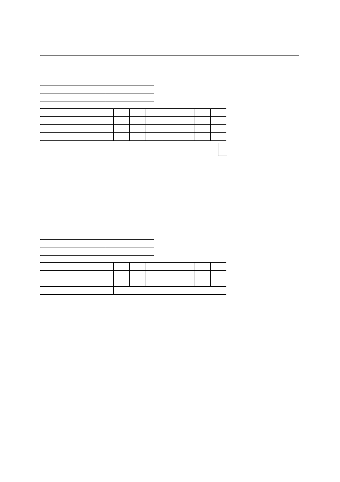
TIMING DIAGRAM
READ Timing (1)
(Address Separate, ADSEL = 0)
PEDL60851C-02
ML60851C¡ Semiconductor
Parameter Symbol Condition Note
Address Setup Time (RD)t
Address Setup Time (CS)t
Address (CS) Hold Time t
Read Data Delay Time t
Read Data Hold Time t
Recovery Time t
FIFO Access Time t
1
1
2
3
4
5
6
(RD)
Load 20 pF
Load 20 pF
FIFO READ
FIFO READ
21 —
0
63
42
Max.Min.
—
25—
250
—
—
Notes: 1. t3 is defined depending upon CS or RD which becomes active last.
is defined depending upon CS or RD which becomes active first.
2. t
2
3. 3-clock time of oscillation clock (clock period: 21 ns). It is required for increment of FIFO.
4. 2-clock time of oscillation clock (clock period: 21 ns). It is required for increment of FIFO.
is required for reading FIFO. t1 is defined when either t1(CS) or t1(RD) is satisfied.
5. t
1
A7:A0
Unit
ns
ns10 — 5(CS)
ns
ns
ns
ns
ns
5
2
1
3
4
CS
RD
AD7:AD0
t
1
t
3
t
6
t
2
t
5
t
4
DATA OUT
48/67

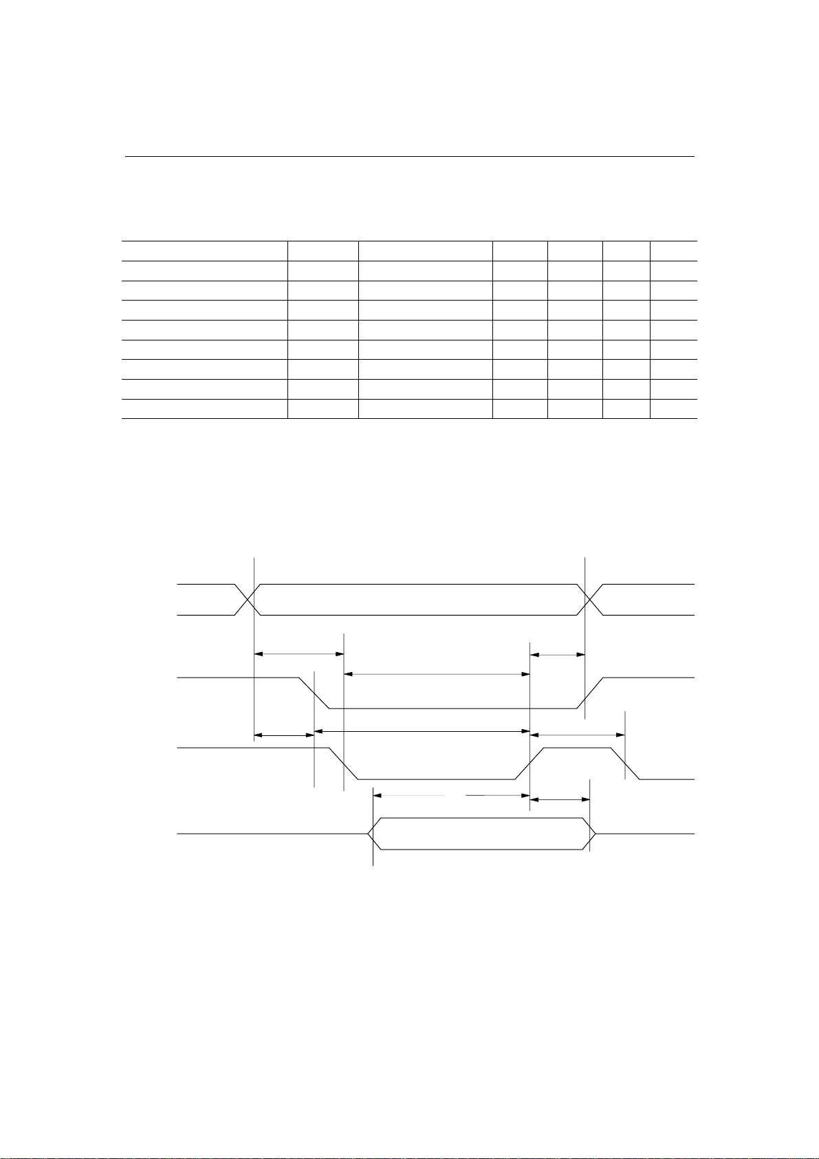
READ Timing (2)
(Address/Data Multiplex, ADSEL = 1)
PEDL60851C-02
ML60851C¡ Semiconductor
Parameter Symbol Condition Note
Address (CS) Setup Time t
Address (CS) Hold Time t
Read Data Delay Time t
Read Data Hold Time t
Recovery Time t
FIFO Access Time t
1
2
3
4
5
6
Load 20 pF
Load 20 pF
FIFO READ
FIFO READ
10 —
0
63
42
Max.Min.
Unit
ns
—
25—
250
—
—
ns
ns
ns
ns
ns
1
2
Notes: 1. 3-clock time of oscillation clock (clock period: 21 ns). It is required for increment of FIFO.
2. 2-clock time of oscillation clock (clock period: 21 ns). It is required for increment of FIFO.
AD7:AD0
CS
t
1
t
2
DATA OUTADDRESS
t
4
ALE
t
3
t
5
RD
t
6
49/67
WRITE Timing (1)
(Address Separate, ADSEL = 0)
PEDL60851C-02
ML60851C¡ Semiconductor
Parameter Symbol Condition Note
Address Setup Time t
Address Setup Time t
Address (CS) Hold Time t
CS Setup Time t
Write Data Setup Time t
Write Data Hold Time t
Recovery Time t
FIFO Access Time t
1
1
2
3
4
5
6
7
FIFO WRITE
FIFO WRITE
Notes: 1. Either t1(a–w) or t1(a–c) should be satisfied.
2. t1 is defined depending upon CS or WR which becomes active first.
3. 3-clock time of oscillation clock (clock period: 21 ns). It is required for increment of FIFO.
4. 2-clock time of oscillation clock (clock period: 21 ns). It is required for increment of FIFO.
5. Applied to all registers including CLRFIFO (address: 4Eh).
A7:A0
t1(a–w)
t
7
CS
Max.Min.
21 —
0
—
—30
—2
63
42
—
—
t
2
Unit
ns
ns10 — 1(a–c)
ns
ns10 —
ns
ns
ns
ns
1(a–w)
2
3
t1(a–c)
3
t
6
t
WR
t
5
AD7:AD0
t
4
DATA IN
50/67

WRITE Timing (2)
(Address/Data Multiplex, ADSEL = 1)
PEDL60851C-02
ML60851C¡ Semiconductor
Parameter Symbol Condition Note
Address (CS) Setup Time t
Address (CS) Hold Time t
Write Data Setup Time t
Write Data Hold Time t
Recovery Time t
FIFO Access Time t
1
2
3
4
5
6
FIFO WRITE
FIFO WRITE
10 —
0
63
42
Max.Min.
Unit
ns
—
—30
—2
—
—
ns
ns
ns
ns
ns
1
2
Notes: 1. 3-clock time of oscillation clock (clock period: 21 ns). It is required for increment of FIFO.
2. 2-clock time of oscillation clock (clock period: 21 ns). It is required for increment of FIFO.
3. Applied to all registers including CLRFIFO (address: 4Eh).
AD7:AD0 ADDRESS DATA IN
t
1
t
2
t
4
CS
ALE
WR
t
3
t
5
t
6
51/67

DMA Transfer Timing (1)
ML60851C to Memory (Single Transfer, Single Address Mode)
PEDL60851C-02
ML60851C¡ Semiconductor
Parameter Symbol Condition Note
DREQ Disable Time t
DREQ Enable Time t
DACK Hold Time t
Read Data Delay Time t
Data Hold Time t
Recovery Time t
1
2
3
4
5
Load 20 pF
Load 20 pF
Load 20 pF
8-bit DMA
6
16-bit DMA
—20
—
0
105
Notes: 1. When in Single Address mode, CS and A7:A0 are ignored.
t1 and t4 are defined depending on DACK or RD which becomes active last.
2. 3-clock time of oscillation clock (clock period: 21 ns).
3. 5-clock time of oscillation clock (clock period: 21 ns).
4. It is possible to increase t2 by setting the DMA interval register (DMAINTVL).
DREQ
DACK
t
1
t
4
t
3
Max.Min.
Unit
ns
63
—0
25—
25
ns
ns
ns
ns
4
1
2ns—63
—3
ns
t
2
t
6
RD
t
5
DOUT
DATA OUT
52/67

DMA Transfer Timing (2)
ML60851C to Memory (Single Transfer, Dual Address Mode)
PEDL60851C-02
ML60851C¡ Semiconductor
Parameter Symbol Condition Note
DREQ Disable Time t
DREQ Enable Time t
Read Data Delay Time t
Data Hold Time
Recovery Time t
1
2
3
t
4
5
Load 20 pF
Load 20 pF
Load 20 pF
8-bit DMA
16-bit DMA
Notes: 1. When in Dual Address mode, the DACK is ignored.
t1 and t3 are defined depending on CS or RD which becomes active last.
A7:A0 specifies the FIFO address.
Refer to READ Timing (1) for Address Setup Time and Address Hold Time.
2. 3-clock time of oscillation clock (clock period: 21 ns).
3. 5-clock time of oscillation clock (clock period: 21 ns).
4. It is possible to increase t2 by setting the DMA interval register (DMAINTVL).
A7:A0
DREQ
Max.Min.
—20
—
63
25—
0
25
—63
105
—3
t
2
Unit
ns
ns
ns
ns
ns
4
1
2ns
CS
RD
DOUT
t
1
t
t
3
t
DATA OUT
5
4
53/67

DMA Transfer Timing (3)
ML60851C to Memory (Demand Transfer, Single Address Mode)
PEDL60851C-02
ML60851C¡ Semiconductor
Parameter Symbol Condition Note
DREQ Disable Time t
DACK Hold Time t
Read Data Delay Time t
Data Hold Time
Recovery Time t
Max.Min.
1
2
3
t
4
Load 20 pF
Load 20 pF
Load 20 pF
—
0—
0
8-bit DMA
5
16-bit DMA
105 3
20
25—
25
—63
—
Unit
ns
ns
ns
ns
ns
1
2ns
Notes: 1. When in Single Address mode, t3 is defined depending on DACK or RD which becomes
active last.
A7:A0 and CS are ignored.
2. 3-clock time of oscillation clock (clock period: 21 ns).
3. 5-clock time of oscillation clock (clock period: 21 ns).
DREQ
t
1
DACK
t
5
t
2
RD
DOUT
t
3
t
4
Last Packet Read
54/67

DMA Transfer Timing (4)
ML60851C to Memory (Demand Transfer, Dual Address Mode)
PEDL60851C-02
ML60851C¡ Semiconductor
Parameter Symbol Condition Note
DREQ Disable Time t
CS Hold Time t
Read Data Delay Time t
Data Hold Time
Recovery Time t
1
2
3
t
4
5
Load 20 pF
Load 20 pF
Load 20 pF
8-bit DMA
16-bit DMA
Notes: 1. When in Dual Address mode, the DACK is ignored.
t3 is defined depending on CS or RD which becomes active last.
A7:A0 specifies the FIFO address.
Refer to READ Timing (1) for Address Setup Time and Address Hold Time.
2. 3-clock time of oscillation clock (clock period: 21 ns).
3. 5-clock time of oscillation clock (clock period: 21 ns).
A7:A0
DREQ
—
0
—
0
63
105
Max.Min.
20
—
25
25
—
—3
Unit
ns
ns
ns
1
ns
2ns
ns
t
1
CS
RD
DOUT
t
5
t
4
t
3
Last Packet Read
t
2
55/67
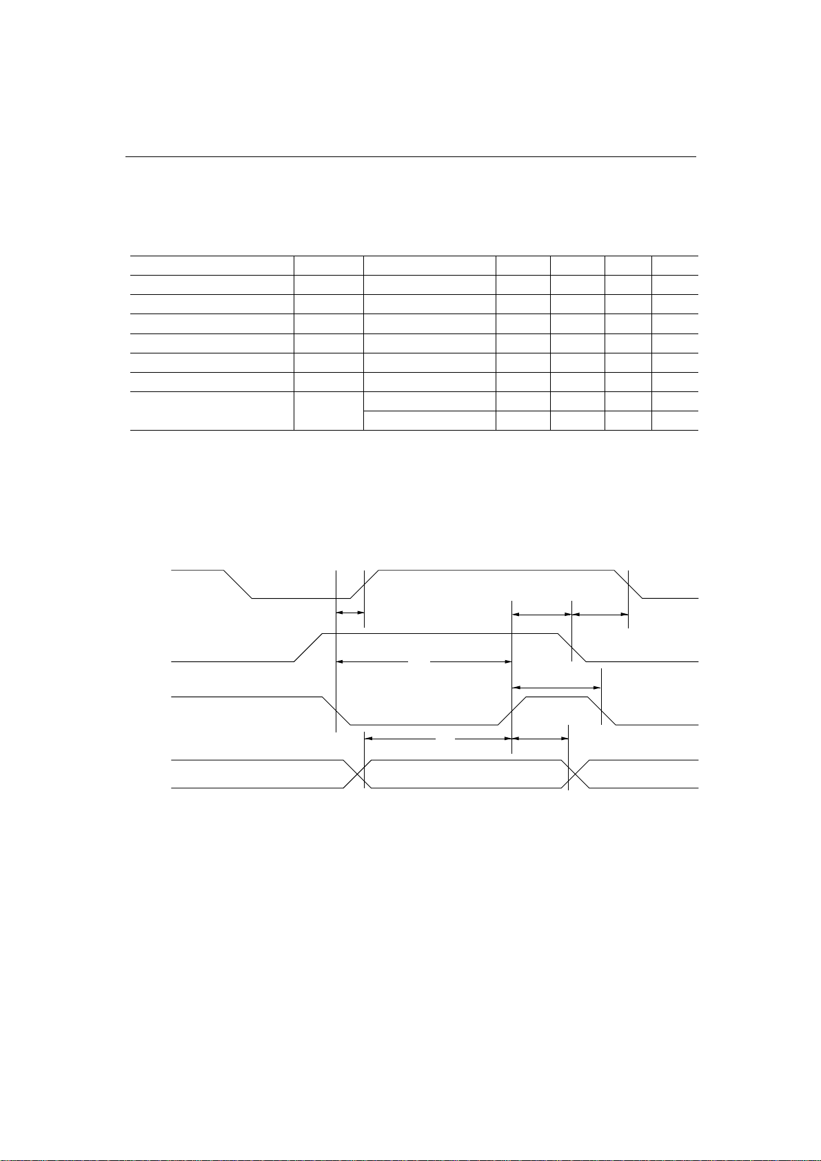
DMA Transfer Timing (5)
Memory to ML60851C (Single Transfer, Single Address Mode)
PEDL60851C-02
ML60851C¡ Semiconductor
Parameter Symbol Condition Note
DREQ Disable Time t
DREQ Enable Time t
FIFO Access Time t
DACK Hold Time
Write Data Setup Time
Write Data Hold Time
Recovery Time
1
2
3
t
4
t
5
t
6
t
7
Load 20 pF
FIFO WRITE
8-bit DMA
16-bit DMA
—20
—
42
30
2
63
105
Notes: 1. When in Single Address mode, CS and A7:A0 are ignored.
2. 3-clock time of oscillation clock (clock period: 21 ns).
3. 5-clock time of oscillation clock (clock period: 21 ns).
4. It is possible to increase t2 by setting the DMA interval register (DMAINTVL).
DREQ
t
4
DACK
t
1
t
3
Max.Min.
Unit
ns
63
—1
—0
—
—
—
—
t
7
ns
4
ns
ns
ns
ns
ns
ns
t
2
2
3
WR
DIN
t
t
5
6
56/67

DMA Transfer Timing (6)
Memory to ML60851C (Single Transfer, Dual Address Mode)
PEDL60851C-02
ML60851C¡ Semiconductor
Parameter Symbol Condition Note
DREQ Disable Time t
DREQ Enable Time t
FIFO Access Time t
Write Data Setup Time
Write Data Hold Time
Recovery Time
1
2
3
t
4
t
5
t
6
Load 20 pF
FIFO WRITE
8-bit DMA
16-bit DMA
Notes: 1. When in Dual Address mode, the DACK is ignored.
t1 and t3 are defined depending on CS or WR which becomes active last.
Refer to WRITE Timing (1) for Address Setup Time and Address Hold Time.
2. 3-clock time of oscillation clock (clock period: 21 ns).
3. 5-clock time of oscillation clock (clock period: 21 ns).
4. It is possible to increase t2 by setting the DMA interval register (DMAINTVL).
A7:A0
DREQ
t
1
Max.Min.
—20
—
42
30
2
63
105
63
—
—
—
—
—
t
2
Unit
ns
ns
ns
ns
ns
ns
ns
4
1
2
3
CS
t
6
t
5
WR
DIN
t
3
t
4
57/67

DMA Transfer Timing (7)
Memory to ML60851C (Demand Transfer, Single Address Mode)
PEDL60851C-02
ML60851C¡ Semiconductor
Parameter Symbol Condition Note
DREQ Disable Time t
FIFO Access Time
DACK Hold Time
Write Data Setup Time t
Write Data Hold Time t
Recovery Time t
1
t
2
t
3
4
5
Load 20 pF
FIFO WRITE
8-bit DMA
6
16-bit DMA
—20
0
30
2
63
105
Notes: 1. When in Single Address mode, A7:A0 and CS are ignored.
t
is defined depending on DACK or WR which becomes active last.
2
2. 3-clock time of oscillation clock (clock period: 21 ns).
3. 5-clock time of oscillation clock (clock period: 21 ns).
DREQ
DACK
t
2
t
6
Max.Min.
Unit
ns
—42
—
—
—
—
—
ns
ns
ns
ns
ns
ns
1
2
3
t
1
t
3
WR
(Note)
DIN
t
4
t
5
Last Packet Write
(Note) The last Write to reach the byte size (maximum packet size) specified by the EP1 Payload
Register.
To terminate DMA transfer before reaching the maximum packet size, set EP1 Packet Ready
by writing "1" to the EP1 Endpoint Packet Ready bit.
58/67

DMA Transfer Timing (8)
(
Memory to ML60851C (Demand Transfer, Dual Address Mode)
PEDL60851C-02
ML60851C¡ Semiconductor
Parameter Symbol Condition Note
DREQ Disable Time t
FIFO Access Time
CS Hold Time
Write Data Setup Time t
Write Data Hold Time t
Recovery Time t
1
t
2
t
3
4
5
6
Load 20 pF
FIFO WRITE
8-bit DMA
16-bit DMA
Notes: 1. When in Dual Address mode, the DACK is ignored.
A7:A0 specifies the FIFO address.
Refer to WRITE Timing (1) for Address Setup Time and Address Hold Time.
t2 is defined depending on CS or WR which becomes active last.
2. 3-clock time of oscillation clock (clock period: 21 ns).
3. 5-clock time of oscillation clock (clock period: 21 ns).
A7:A0
DREQ
Max.Min.
—20
42
0
30
2
63
105
—
—
—
—
—
—
t
1
Unit
ns
ns
ns
ns
ns
ns
ns
1
2
3
CS
t
3
(Note)
WR
DIN
t
2
t
4
Note) Refer to the previous page.
t
6
t
5
Last Packet Write
59/67

FUNCTIONAL DESCRIPTIONS
Pin Functional Description
USB Interface
PEDL60851C-02
ML60851C¡ Semiconductor
Signal
D+
Type
I/O
—
—I/OD–
USB data (Plus). This signal and the D– signal are the transmitted or received
data from/to USB Bus. The table below shows values and results for these signals.
D+ D– Result
0 0 Single end 0
0 1 Differential "0"
1 0 Differential "1"
1 1 Undefined
USB Data (Minus). This signal and the D+ signal are the transmitted or
received data from/to USB Bus. The table above shows values and results for
these signals.
DescriptionAssertion
Crystal Oscillator Interface
Signal
XIN For internal oscillation, connect a crystal to XIN and XOUT.
Type
I
—
—OXOUT
For external oscillation, supply an external 48 MHz clock signal to XIN.
Set XOUT to be open.
DescriptionAssertion
60/67

Application Interface
PEDL60851C-02
ML60851C¡ Semiconductor
Signal
D15:D8
Type
I/O
OINTR
ODREQ
IDACK
IALE
IADSEL
IRESET
—
—I/OAD7:AD0
—IA7:A0
LOWICS
LOWIRD
LOWIWR
LOW
(Note 1)
LOW
(Note 1)
HIGH
(Note 1)
—
—
LOW
DescriptionAssertion
Upper byte (MSB) of data bus. This data bus is used by applications to access
register files and FIFO data.
Lower byte (LSB) of data bus when ADSEL is LOW.
Address and lower byte of data bus are multiplexed when ADSEL is HIGH.
Address when ADSEL is LOW. This address signal is used by application to
access register files and FIFO data.
This signal is ignored (all lows or all highs) when ADSEL is HIGH.
Chip Select. When this signal is asserted LOW, the ML60851C is selected
and ready to read or write data.
Read Strobe. When this signal is asserted LOW, the Read instruction is
executed.
Write Strobe. When this signal is asserted LOW, the Write instruction is
executed.
Interrupt Request. When this signal is asserted, the ML60851C makes an
interrupt request to the application.
DMA Request. This signal requests the Endpoint FIFO to make a DMA transfer.
DMA Acknowledge Signal. This signal, when asserted, enables accessing
FIFOs, without address bus setting.
When ADSEL is HIGH, the address and CS on AD7:AD0 is latched at the
trailing edge of this signal. This signal is ignored when ADSEL is LOW.
When ADSEL is LOW, the address is input on A7:A0 and data is input on
D15:D8 and AD7:AD0. When ADSEL is HIGH, the lower bytes (LSB) of
address and data are multiplexed on AD7:AD0.
System Reset. When this signal is asserted LOW, the ML60851C is reset.
When the ML60851C is powered on, this signal must be asserted for 1 ms or more.
Note: 1. Initial value immediately after resetting. Its assertion can be changed by programming.
61/67

PEDL60851C-02
ML60851C¡ Semiconductor
Functional Description
The ML60851C USB device controller contains the Protocol Engine, DPLL, Timer, Status/Control,
FIFO Control, Application Interface, and Remote Wakeup blocks.
• Protocol Engine
The Protocol Engine handles the USB communication protocol. It performs control of packet
transmission/reception, generation/detection of synchronous patterns, CRC generation/checking,
NRZI data modulation, bit stuffing, and packet ID (PID) generation/checking.
• DPLL (Digital Phase Locked Loop)
The DPLL extracts clock and data from the USB differential received data (D+ and D–).
• Timer
The Timer block monitors idle time on the USB bus.
• Status/Control
The Status Control block moniors the transaction status and transmits control events to the
application through an interrupt request.
62/67

PEDL60851C-02
ML60851C¡ Semiconductor
• FIFO Control
The FIFO Control block controls all FIFO operations for transmitting and receiving USB packets.
The FIFO configuration is described below.
Endpoint FIFO/8-Byte Setup Register Configuration
Endpoint Address 0
Endpoint Address 0
Endpoint Address 0
Endpoint Address 1
Endpoint Address 2
8-Byte
Setup Register
8-Byte
FIFO Rx
8-Byte
FIFO Tx
64-Byte
FIFO
64-Byte
FIFO
64-Byte
FIFO
For Control Transfer
Setup Ready
Packet Ready
Packet Ready
For Bulk Transfer
Packet Ready
DMA Request
Packet Ready
EP0 Receive FIFO
EP0 Transmit FIFO
EP1 FIFO (128 bytes)
(Selectable for transmitter
or receiver)
EP2 FIFO (64 bytes)
(Selectable for transmitter
or receiver)
Endpoint Address 3
Endpoint address Program sizeFIFO type
Reception
Transmission
Reception/Transmission
8-Byte
FIFO
Packet Ready
EP3 FIFO (8 bytes)
Function
0
0
1
8 Bytes
8 Bytes
64 Bytes (2 levels)
Transfer control
Transfer control
Bulk-In and bulk-Out
Reception/Transmission 2 64 Bytes Bulk-Out and bulk-In
Transmission
3
8 Bytes
Interrupt
Every FIFO has a flag that indicates a full or empty FIFO and the capability of re-transmitting and
re-receiving data. Endpoint addresses 1 and 2 can be used for either of reception and transmission
by writing the register.
The FIFO at endpoint address 1 can be used for DMA transfer.
63/67

PEDL60851C-02
ML60851C¡ Semiconductor
• Interrupt
Interrupt factors include Packet Ready for a transmit/receive FIFO, Setup Ready for 8-byte setup
data, and Suspend. Generation of each interrupt request can be enabled or disabled by the
Interrupt Enable register.
•DMA
8-bit and 16-bit demand transfer DMA and single transfer DMA are enabled for bulk-transfer FIFO
at endpoint address 1.
In Demand Transfer mode, DREQ is asserted when a valid packet arrives at the FIFO. When the
external DMA contoller has completed transferring all byte data of a received packet, DREQ is
deasserted. Accordingly, other devices cannot access the local bus during DMA transfer.
In Single Tranfer mode, each time transfer of one byte data is completed, DREQ is deasserted.
While DREQ is deasserted, other devices can access the local bus.
• Remote Wakeup
This functional block supports the remote wakeup function.
• USB Transfers
The ML60851C supports the two transfer types (Control Transfer and Bulk Transfer) of four
transfer types (Control, Isochronous, Interrupt, and Bulk) defined by the USB Specifications.
- The Control Transfer is required for transfer of configuration, commands, and status information
between the host and devices.
- The Bulk Transfer enables transfer of a large amount of data when the bus bandwidth is enough.
• USB Transceiver
The ML60851C contains an Oki's USB transceiver which converts internal unidirectional signals
into USB-compatible signals.
This enables the designer's application module to interface to the physical layer of the USB.
64/67

EXAMPLE OF OSCILLATOR CIRCUIT
• Oscillation Circuit Example 1
ML60851C
PEDL60851C-02
ML60851C¡ Semiconductor
XIN
XOUT
Rf
C2
C3
L1
Crystal: HC-49U (KINSEKI, LTD)
C2 = 5 pF
C3 = 1000 pF
Rf = 1 MW
L1 = 2.2 mH
Note: The example shown above is not guaranteed for circuit operation.
• Oscillation Circuit Example 2
ML60851C
CSTCW4800MX41xxx
XIN
XOUT
Rf
Ceramic oscillator: CSTCM4800MXxxx (MURATA MFG.)
(C-built-in type)
Note: The example shown above is not guaranteed for circuit operation.
65/67

PACKAGE DIMENSIONS
QFP44-P-910-0.80-2K
Mirror finish
PEDL60851C-02
ML60851C¡ Semiconductor
(Unit : mm)
Package material
Lead frame material
Pin treatment
Solder plate thickness
Package weight (g)
Epoxy resin
42 alloy
Solder plating
5 mm or more
0.41 TYP.
Notes for Mounting the Surface Mount Type Package
The SOP, QFP, TSOP, SOJ, QFJ (PLCC), SHP and BGA are surface mount type packages, which
are very susceptible to heat in reflow mounting and humidity absorbed in storage.
Therefore, before you perform reflow mounting, contact Oki’s responsible sales person for the
product name, package name, pin number, package code and desired mounting conditions
(reflow method, temperature and times).
66/67

TQFP44-P-1010-0.80-K
Mirror finish
PEDL60851C-02
ML60851C¡ Semiconductor
(Unit : mm)
Package material
Lead frame material
Pin treatment
Solder plate thickness
Package weight (g)
Epoxy resin
42 alloy
Solder plating
5 mm or more
0.28 TYP.
Notes for Mounting the Surface Mount Type Package
The SOP, QFP, TSOP, SOJ, QFJ (PLCC), SHP and BGA are surface mount type packages, which
are very susceptible to heat in reflow mounting and humidity absorbed in storage.
Therefore, before you perform reflow mounting, contact Oki’s responsible sales person for the
product name, package name, pin number, package code and desired mounting conditions
(reflow method, temperature and times).
67/67
 Loading...