

Page 1

UM10468
SSL2108X buck evaluation board
Rev. 1 — 30 August 2011 User manual
Document information
Info Content
Keywords SSL2108X, Buck, down converter, AC/DC conver te r, retrofit SSL, LED
driver, LED retrofit lamp, non-dimmable
Abstract The SSL2108X is a range of high-voltage Integrated Circuits (ICs),
intended to drive non-dimmable retrofit LED lamps in general lighting
applications. This document describes the evaluation board for mains
operated non-dimmable LED drivers using the SSL21081, SSL21082,
SSL21083 and SSL21084 controller ICs.
Refer to the SSL2108X data sheet for details on the SSL2108X device
and application note AN11041 for general application information.
Page 2

NXP Semiconductors
UM10468
SSL2108X buck evaluation board
Revision history
Rev Date Description
v.1 20110830 first issue
Contact information
For more information, please visit: http://www.nxp.com
For sales office addresses, please send an email to: salesaddresses@nxp.com
UM10468 All information provided in this document is subject to legal disclaimers. © NXP B.V. 2011. All rights reserved.
User manual Rev. 1 — 30 August 2011 2 of 27
Page 3
NXP Semiconductors
1. Introduction
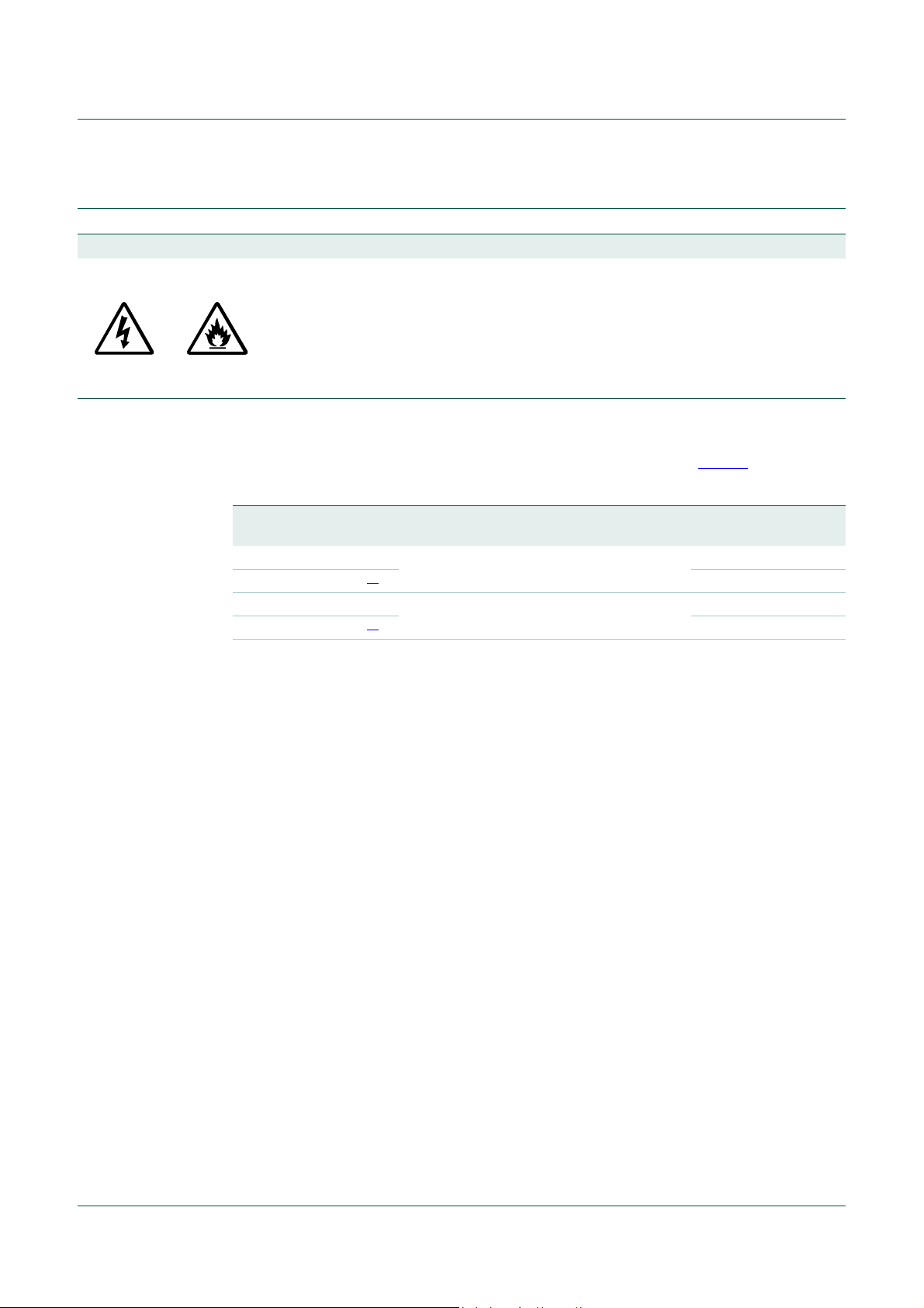
WARNING
Lethal voltage and fire ignition hazard
The non-insulated high voltages that are present when operating this product, constitute a
risk of electric shock, personal injury, death and/or ignition of fire.
This product is intended for evaluation purposes only. It shall be operated in a designated test
area by personnel qualified according to local requirements and labor laws to work with
non-insulated mains voltages and high-voltage circuits. This product shall never be operated
unattended.
The SSL2108X is a family of high-voltage Integrated Circuits (IC), designed to drive
non-dimmable retrofit LED lamps in general lighting applications. The product family
consists of four ICs with different configurations which are shown in Table 1
Table 1. SSL2108X type number overview
Type Package V
SSL21081 SO8 100 to 120 300 V; 2 no
SSL21082 SO12
SSL21083 SO8 100 to 230 600 V; 5 no
SSL21084 SO12
[1]
[1]
mains
(V (AC))
range
SSL2108X buck evaluation board
Internal MOSFET
characteristics
UM10468
.
Adjustable brownout
protection
yes
yes
[1] SO12 package variants have more fused leads for lower thermal resistance and can be used when a higher
output power is needed.
Main benefits of the product family are:
• Small Printed-Circuit Board (PCB) footprint providing a compact solution
• High-efficiency (up to 95 %)
• Ease of integration
• Low electronic Bill Of Material (BOM)
The SSL2108X provides accurate output control with more than 5 % LED current
accuracy. The ICs can operate using Pulse-Width Modulation (PWM) dimming and have
many protection features including easy external temperature feedback.
The SSL2108X driver family is the high performance solution for the next generation of
retrofit LED lamps. These ICs provide a high efficiency, high-power factor solution in a
small form factor.
Remark: Unless otherwise stated all voltages are in V (DC).
UM10468 All information provided in this document is subject to legal disclaimers. © NXP B.V. 2011. All rights reserved.
User manual Rev. 1 — 30 August 2011 3 of 27
Page 4
NXP Semiconductors
019aab173
019aab174
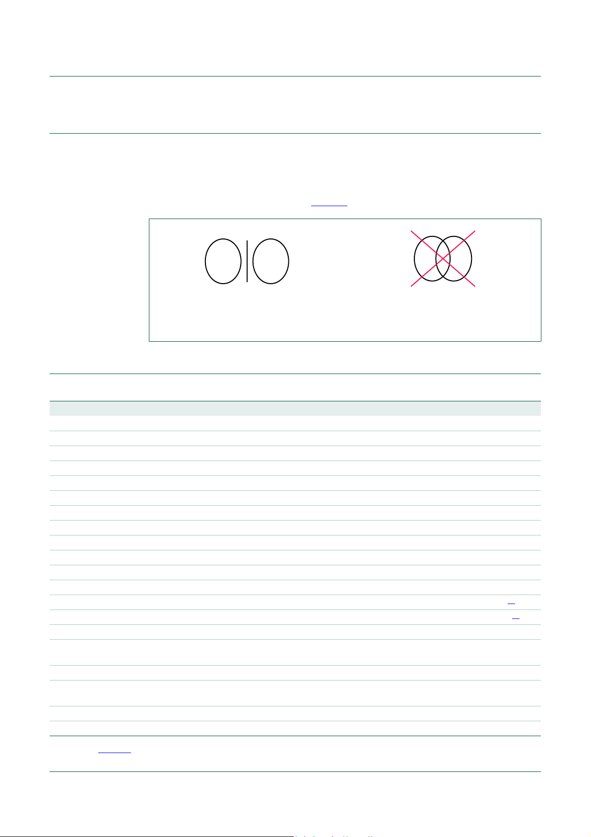
2. Safety warning
This reference board is connected to a high AC voltage (up to 250 V). Avoid touching the
demo board during operation. An isolated housing is obligatory when used in
uncontrolled, non-laboratory environments. Galvanic iso lation of the ma ins p hase using a
fixed or variable transformer (Variac) is always recommended. These devices are
recognized by the symbols shown in Figure 1
Fig 1. Variac isolation symbols
UM10468
SSL2108X buck evaluation board
a. Isolated b. Not isolated
3. Specification
LED
LED
)
)
)
o(LED)
100 kHz -
70 mm 60 mm 23 mm maximum footprint
Table 2. Specifications for the reference board
Parameter Value Comment
AC line input voltage
SSL21081 and SSL21082 85 V (AC) to 138 V (AC) optimized for 100 V (AC)
SSL21083 and SSL21084 230 V (AC) optimized for 100 V (AC)
Output voltage (V
SSL21081 and SSL21082 20 V to 70 V optimized for 60 V
SSL21083 and SSL21084 20 V to 140 V optimized for 120 V
Output current (I
SSL21081 95 mA, 70 mA, 38 mA adjust using jumpers J7A, J8A, J9A
SSL21082 160 mA, 125 mA, 105 mA adjust using jumpers J7A, J8A, J9A
SSL21083 55 mA, 35 mA, 18 mA adjust using jumpers J7A, J8A, J9A
SSL21084 80 mA, 69 mA, 53 mA adjust using jumpers J7A, J8A, J9A
Maximum LED output power (P
SSL21081 and SSL21083 6 W optimized for 6 W using dedicated loads
SSL21082 and SSL21084 15 W optimized for 10 W using dedicated loads
Switching frequency
Nominal switching frequency
sw(nom)
)
(f
Board dimension (L W H)
SSL21081, SSL21082, SSL21083
and SSL21084
Temperature
Operating temperature 40 Cto +100C-
[1]
[1]
[1] Refer to Section 5 for more detailed information.
UM10468 All information provided in this document is subject to legal disclaimers. © NXP B.V. 2011. All rights reserved.
User manual Rev. 1 — 30 August 2011 4 of 27
Page 5
NXP Semiconductors
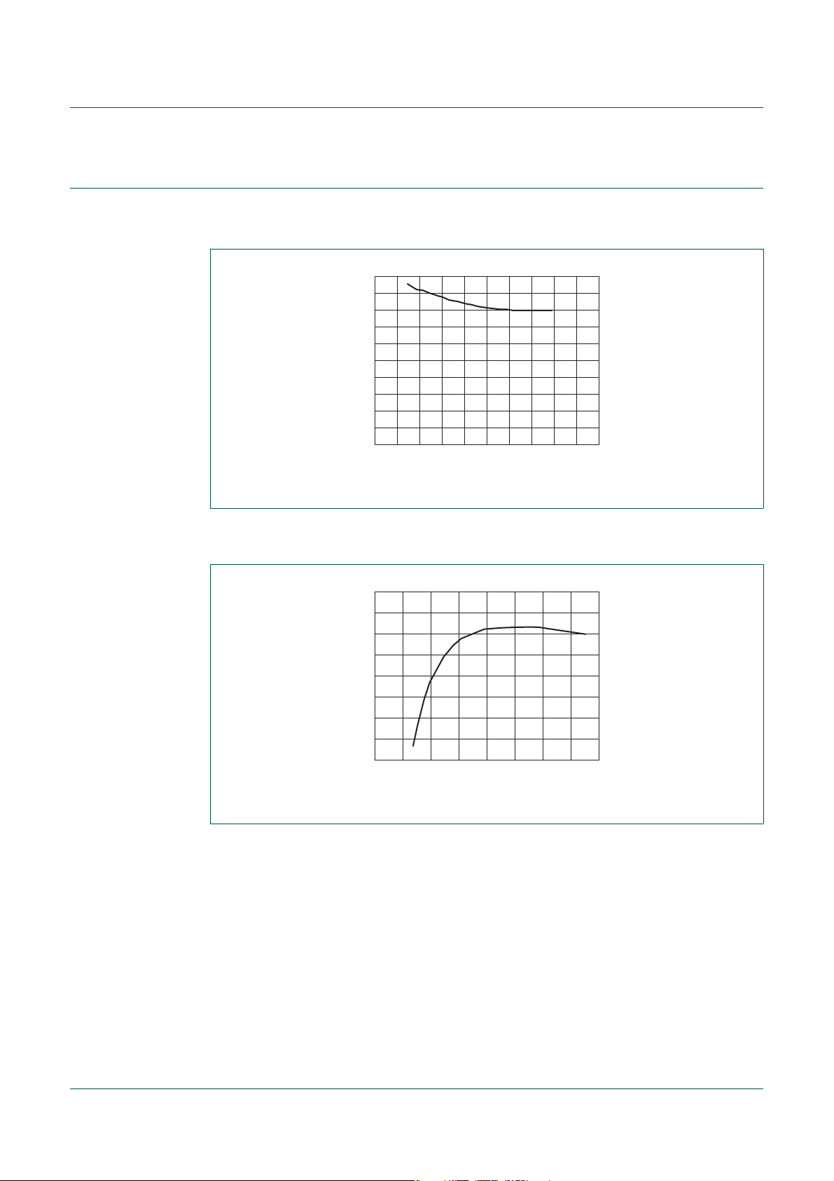
4. Performance data
4.1 Output load
UM10468
SSL2108X buck evaluation board
Fig 2. SSL21081 load curve: Io as a function of V
4.2 Efficiency Curve
l
o
(mA)
120
100
80
60
40
20
92
η
(%)
90
88
0 1008040 6020
019aac361
(V)
V
o
o
019aac362
86
84
08624
(W)
P
o
Fig 3. SSL21081: Efficiency () as a function of output power (Po)
UM10468 All information provided in this document is subject to legal disclaimers. © NXP B.V. 2011. All rights reserved.
User manual Rev. 1 — 30 August 2011 5 of 27
Page 6
NXP Semiconductors
40
80
120
l
o
(mA)
0
V
mains
(V)
40 14012080 10060
019aac363
4.3 Input voltage dependency
UM10468
SSL2108X buck evaluation board
Fig 4. SSL21081 input voltage dependency: Io as a function of V
4.4 ElectroMagnetic Compatibility data
= V
mains
(1)
(2)
019aac364
IN
(1) Peak values.
(2) Average values.
Fig 5. SSL21081 EMC measurement L-phase according to FCC15 norm
UM10468 All information provided in this document is subject to legal disclaimers. © NXP B.V. 2011. All rights reserved.
User manual Rev. 1 — 30 August 2011 6 of 27
Page 7

NXP Semiconductors
019aac365
(1)
(2)
UM10468
SSL2108X buck evaluation board
(1) Peak values.
(2) Average values.
Fig 6. SSL21081 EMC measurement N-phase according to FCC15 norm
(1) Peak values.
(2) Average values.
Fig 7. SSL21083 EMC measurement L-phase according to EN55015 norm
UM10468 All information provided in this document is subject to legal disclaimers. © NXP B.V. 2011. All rights reserved.
User manual Rev. 1 — 30 August 2011 7 of 27
Page 8

NXP Semiconductors
UM10468
SSL2108X buck evaluation board
(1) Peak values.
(2) Average values.
Fig 8. SSL21083 EMC measurement N-phase according to EN55015 norm
UM10468 All information provided in this document is subject to legal disclaimers. © NXP B.V. 2011. All rights reserved.
User manual Rev. 1 — 30 August 2011 8 of 27
Page 9
NXP Semiconductors
019aac366
(1)
(2)
4.5 SSL21081 mains harmonics
Table 3. SSL21081 mains conducted harmonics
Line Percent (%) Class-C Except Line Percent (%) Class-C Except
1 100 100 100 21 5.9 3 undefined
2 0 2 undefined 22 0 2 undefined
3 84.7 30 86 23 4.4 3 undefined
4 0 2 undefined 24 0.4 2 undefined
5 59.8 10 61 25 3.8 3 undefined
6 0 2 undefined 26 0.4 2 undefined
7 34.1 7 undefined 27 3.6 3 undefined
8 0 2 undefined 28 0 2 undefined
9 17.9 5 undefined 29 3.2 3 undefined
10 0 2 undefined 30 0 2 undefined
11 15.4 3 undefined 31 2.2 3 undefined
12 0 2 undefined 32 0.2 2 undefined
13 13.9 3 undefined 33 2.2 3 undefined
14 0 2 undefined 34 0.2 2 undefined
15 9.7 3 undefined 35 2 3 undefined
16 4.5 2 undefined 36 0.4 2 undefined
17 7 3 undefined 37 1.9 3 undefined
18 0.6 2 undefined 38 0 2 undefined
19 6.8 3 undefined 39 1.4 3 undefined
20 0.3 2 undefined 40 0 2 undefined
UM10468
SSL2108X buck evaluation board
(1) Input voltage VIN.
(2) Input current I
.
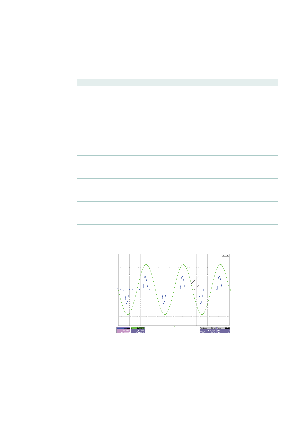
I
Fig 9. VIN and II for a 100 V; 60 Hz AC mains supply
UM10468 All information provided in this document is subject to legal disclaimers. © NXP B.V. 2011. All rights reserved.
User manual Rev. 1 — 30 August 2011 9 of 27
Page 10

NXP Semiconductors
019aac367
(1)
(2)
UM10468
SSL2108X buck evaluation board
(1) Drain voltage V
(2) Source voltage V
Fig 10. V
DRAIN
and V
.
DRAIN
SOURCE
SOURCE
.
typical waveforms
UM10468 All information provided in this document is subject to legal disclaimers. © NXP B.V. 2011. All rights reserved.
User manual Rev. 1 — 30 August 2011 10 of 27
Page 11

NXP Semiconductors
5. Connection data
The evaluation board operates from either:
• SSL21081 and SSL21082: 100 V (AC) to 120 V (AC) mains supply voltage
• SSL21083 and SSL21084: 230 V (AC) mains supply voltage
The evaluation board is designed to work with an LED module with an operating voltage
of:
• SSL21081 and SSL21082: 60 V
• SSL21083 and SSL21084: 120 V
Loads consisting of multiple high-power LEDs in series with similar operating voltages can
also be used. A dedicated SHARP GW5BDQ27KK3 LED load for connecting to conn ector
K2A is available on request. Other loads can be connected to either connector K2A or K3.
When attaching an LED load to a board under power (hot plugging), an inrush peak
current occurs due to discharge of capacitor C3. After several discharges, the LEDs will
deteriorate or become damaged.
UM10468
SSL2108X buck evaluation board
Jumper settings J1A to J6A shown in Table 4
each device to function correctly.
Table 4. SSL2108X jumper settings overview
IC Package Jumper settings
J1A J2A J3A J4A J5A J6A
SSL21081 SO8 no yes no yes no yes
SSL21083
SSL21082 SO12 yes no yes no yes no
SSL21084
set the package-specific circuitry to enable
5.1 The board connections
When connecting the evaluation board consider the following:
• Place a galvanic isolated transformer between the AC source and the evaluation
board connector K1A, if used.
• Connect a user-defined LED module to connector K2A or K3. Ensure that the anode
of the LED module is connected to one of the positive LED terminals.
• Connector K4 can be used:
– to connect an external NTC resistance. Remove the pre-soldered NTC RT1 (see
)
Ref. 1
– to use a PWM dimming signal to the converter (see Ref. 1
)
UM10468 All information provided in this document is subject to legal disclaimers. © NXP B.V. 2011. All rights reserved.
User manual Rev. 1 — 30 August 2011 11 of 27
Page 12

NXP Semiconductors
UM10468
SSL2108X buck evaluation board
external NTC/
PWM input
NTC -
NTC +
mains
input
Fig 11. Board connection diagram
6. Functional description
The SSL2108X IC (Ref. 1) uses Boundary Conduction Mode (BCM) with peak current
control. The SSL2108X controls and drives the converter. In addition, the SSL2108X
offers a low component count LED buck converter solution . Valley switching and PWM
dimming are implemented into the SSL2108X together with several protection features:
J10
C3
K3
LED +
J5
J6
D2
K2
C1D1C8
L1
019aac358
LED -
LED +
LED -
LED load
LED load
X55
IC1
L3
D3
C2
J9
J8
J7
RT1
K4
K1
L
N
J3
J2
J1
J4
FUSE 1
L2
• UnderVoltage LockOut (UVLO)
• Leading-Edge Blanking (LEB)
• OverCurrent Protection (OCP)
• Internal OverTemperature Protection (OTP)
• Brownout protection
• Short-Winding Protection (SWP)
• Output Short Protection (OSP)
• NTC over temperature control and protection
Both the SWP and the OSP are latched protections circuits. These protective features
cause the IC to halt until a reset is executed. If V
resets the latched protection mode. Restarting the evaluation board is done by removing
AC mains supply voltage. All other protective features cause a safe restart of the
converter. Refer to the SSL2108X data sheet for detailed information on all protective
features.
Depending on the selected SSL2108X version, the evaluation board is optimized for an
LED voltage, LED current and resulting output power. See Table 2
J7A is set to apply the full output power to the LED load. Setting jumper J8A or J9A
instead reduces the output power to either 66 % or 33 % of the original output power.
Remark: Do not remove or set jumpers when the board is connected to the AC mains
supply voltage because LED damage can occur.
drops below its restart level, the IC
CC
. As a default, jumper
UM10468 All information provided in this document is subject to legal disclaimers. © NXP B.V. 2011. All rights reserved.
User manual Rev. 1 — 30 August 2011 12 of 27
Page 13

NXP Semiconductors
Jumper J10A is connected in series with the brownout capacitor C8. Removing this
jumper sets the brownout protection trigger values to be reset to default value.
Remark: Brownout protection is only available in the SSL21082 and SSL21084.
TVS Diode D2 is present to protect the DC circuit against overvoltage.
7. Board optimization
The EMC filter calculations for components C1, C2, L1 are described in AN11041 (see
Ref. 2
). On the evaluation board, L2 and C8 have been added to provide extra filtering to
meet EMC norms.
Power factor of the evaluation board depends mainly on the input resistance of the input
fused resistor FUS1. A higher resistance proportionally increases the power factor but
reduces the overall efficiency of the evaluation board.
Another way to get higher power factor is to add a valley fill circuit. The valley fill circuit
improves power factor with reduced efficiency losses. The disadvantage is the higher
component count needed. Figure 12
resistance as a function of power factor and efficiency.
UM10468
SSL2108X buck evaluation board
gives an overview for the SSL21081 of input
019aac359
R
(Ω)
in
PF
0.8
0.6
0.4
0.2
0.0
η
(%)
(1) Efficiency curve.
(2) Power factor curve.
94
90
86
82
78
0 1208040
(1)
(2)
Fig 12. Input resistance (RIN) as a function of Power Factor (PF) and Efficiency ()
Remark: Calculations for other components on the SSL2108X evaluation board can be
found in AN11041 (see Ref. 2
).
UM10468 All information provided in this document is subject to legal disclaimers. © NXP B.V. 2011. All rights reserved.
User manual Rev. 1 — 30 August 2011 13 of 27
Page 14

NXP Semiconductors
019aac538
56 Ω
1 MΩ
MCR22-6
22 nF
7.1 Active bypass
An increased value for the inrush current resistor causes the board to operate with the
most phase cut dimmers, but also lowers the efficiency. If a higher power factor is not
required, but leading-edge dimmer compatibility and high efficiency are important, the
active bypass option is available. In this circuit, the inrush current resistor is bypassed
using an SCR (see Figure 13
Fig 13. Active bypass
UM10468
SSL2108X buck evaluation board
).
UM10468 All information provided in this document is subject to legal disclaimers. © NXP B.V. 2011. All rights reserved.
User manual Rev. 1 — 30 August 2011 14 of 27
Page 15

NXP Semiconductors
SSL2108X buck evaluation board
8. Negative Temperature Coefficient (NTC) function
The NTC pin can act as a control for thermal protection, an input for disabling/enabling the
light output using PWM dimming and a soft-start function.
When using the NTC pin as a control for thermal protection, the pre-soldered NTC RT1
can be used. Alternatively, a user-defined NTC resistor can be directly connected to this
pin through connector K4. Remove the pre-soldered NTC RT 1 in this case. If necessar y, a
resistor R6 can be mounted to fine-tune the NTC protection. As the default, a 0
resistance is mounted.
In addition, a PWM signal can be connected to connector K4, making PWM dimming
possible. Capacitor C7 is used as the soft-start capacitor. When using the soft-start
capacitor, the NTC protection function changes from auto-restart protection to a latched
protection.
Remark: Detailed information on the NTC function can be found in the SSL2108X
data sheet (see Ref. 1
).
UM10468
UM10468 All information provided in this document is subject to legal disclaimers. © NXP B.V. 2011. All rights reserved.
User manual Rev. 1 — 30 August 2011 15 of 27
Page 16

NXP Semiconductors
9. Schematic
K1 K2
FUS 1
L1
UM10468
SSL2108X buck evaluation board
K3
LED+
LED-
L1
LED+
to mains
RGND
TP2
test point
R5
earth
N
D1
C8
RGND
L2
D2
C1
TP3
test point
D3
C3C2
LED-
to LED’s
L3
R1R2R3R4
J7J8J9
C6
C7
test point
J1
J2
J3
J4
test point
RT1
NTC
R6
TP1
TP2
NTC+
NTC-
n.c.
GND
VCC
NTC
GND
S
K4
IC1
1
2
3
4
5
6
7
(SOURCE)
(VCC)
(NTC)
SSL21081/
SSL21083
SSL21082/
SSL21084
TP4
test point
(GND)
(DVDT)
test point
TP2
14
13
12
11
10
9
8
DRAINHV
n.c.
GND
GND
DVDT
TONMAX
GND
TP7
test point
J5
J6
C4
TP6
test point
J10
TP5
test point
C6
019aac360
Fig 14. Schematic
UM10468 All information provided in this document is subject to legal disclaimers. © NXP B.V. 2011. All rights reserved.
User manual Rev. 1 — 30 August 2011 16 of 27
Page 17

NXP Semiconductors
UM10468
SSL2108X buck evaluation board
10. Bill of materials (BOM)
10.1 BOM for SSL21081 evaluation board
Table 5. SSL21081 Bill of materials
Ref. Description and value Manufacturer and part no. Remark
A1 SSL21081 controller IC NXP Semiconductors A1A IC socket Wells-cti; 652B0142211-002 not mounted
C1 filter capacitor; 10 F; 200 V Nichicon; UVZ2D100MPD1TD C2 filter capacitor; 10 F; 200 V Nichicon; UVZ2D100MPD1TD C3 ripple capacitor; 2.2 F; 450 V Panasonic; ECA2WHG2R2 C4 dV/dt capacitor; 2 kV; 150 pF Multicomp; MCCA000740 C5 VCC supply; capacitor; 10 F; 25 V Murata; GRM21BR61E106KA73L C6 t
C7 soft-start/ripple filter; 22 F; 10 V Kemet; C1206C226M8PACTU C8 filter capacitor - not mounted
D1 bridge rectifier; 1 A; 600 V Multicomp; DBLS105G D2 TVS; 200 V; 1.5 KW ST Microelectronics; 1.5KE 200A D3 ES1J; 1 A; 600 V Multicomp; ES1J Fus 1 fused resistor; 2 W; 10 R Welwyn; EMC2-10RK J1 to J9 headers Fischer Elektronik; MK 05/50G J10 header Fischer Elektronik; MK 05/50G not mounted
J1A jumper Lumberg; 2,54MKB not mounted
J2A jumper Lumberg; 2,54MKB J3A jumper Lumberg; 2,54MKB not mounted
J4A jumper Lumberg; 2,54MKB J5A jumper Lumberg; 2,54MKB not mounted
J6A jumper Lumberg; 2,54MKB J7A jumper Lumberg; 2,54MKB J8A jumper Lumberg; 2,54MKB not mounted
J9A jumper Lumberg; 2,54MKB not mounted
J10A jumper Lumberg; 2,54MKB not mounted
K1 header Weidmuller; SL 5.08/3/90 K1A socket Weidmuller; BL 5.08/3 K2 header Weidmuller; SL 5.08/2/90 K2A socket Weidmuller; BL 5.08/2 K3 header Fischer Elektronik; BL3.36Z K4 header Fischer Elektronik; BL3.36Z L1 filter inductor; 1 mH; 170 mA Murata power solutions; 22R105C L2 filter inductor; Short - L3 buck inductor; 1 mH; 0.5 A Wurth elektronik; 768772102 R1 R
R2 R
on(max)
sense
sense
capacitor - not mounted
; 6.8 ; 0.33 W; 1 % Panasonic; ERJ8BQF6R8V ; 3.3 ; 0.33 W; 1 % Panasonic; ERJ8BQF3R3V -
UM10468 All information provided in this document is subject to legal disclaimers. © NXP B.V. 2011. All rights reserved.
User manual Rev. 1 — 30 August 2011 17 of 27
Page 18

NXP Semiconductors
UM10468
SSL2108X buck evaluation board
Table 5. SSL21081 Bill of materials
…continued
Ref. Description and value Manufacturer and part no. Remark
R3 R
R4 R
; 5.1 0.25 W; 1 % Vishay dale; CRCW12065R10FKEA -
sense
; 16 ; 0.25 W; 1 % VIshay dale; CRCW120616R0FKEA -
sense
R5 inrush resistor; 0 Multicomp; MC 0.1W 0805 0R R6 resistor; 0 Multicomp; MC 0.1W 0805 0R RT1 NTC; 100 k EPCOS; B57164K104J TP1 to TP8 test pins Vero; 20-313138 X56 jumper link Fischer Elektronik; 2412 015 30123 X57 jumper link; Fischer Elektronik; 2412 015 30123 -
10.2 BOM for SSL21082 evaluation board
Table 6. SSL21082 Bill of materials
Ref. Description and value Manufacturer and part no. Remark
A1 SSL21082 Controller IC NXP Semiconductors; SSL21082T A1A IC Socket; n.m. Wells-cti; 652B0142211-002 not mounted
C1 filter capacitor; 10 F; 200 V Nichicon; UVZ2D100MPD1TD C2 filter capacitor; 10 F; 200 V Nichicon; UVZ2D100MPD1TD C3 ripple capacitor; 2.2 F; 450 V Panasonic; ECA2WHG2R2 C4 dV/dt capacitor; 150 pF; 2000 V Multicomp; MCCA000740 C5 VCC supply capacitor; 10 µF; 25 V MURATA; GRM21BR61E106KA73L C6 t
on(max)
C7 soft-start/ripple filter; 22 F; 10 V KEMET; C1206C226M8PACTU C8 filter capacitor; n.m. - not mounted
D1 bridge rectifier; 1 A; 600 V Multicomp; DBLS105G D2 TVS; 200 V; 1.5 kW ST Microelectronics; 1.5KE200A D3 ES1J; 1 A; 600 V Multicomp; ES1J Fus 1 fused resistor; 2 W; 10 Welwyn; EMC2-10RK J1 to J9 headers Fischer Elektronik; MK 05/50G J10 header Fischer Elektronik; MK 05/50G J1A jumper Lumberg; 2,54MKB J2A jumper; n.m. Lumberg; 2,54MKB not mounted
J3A jumper Lumberg; 2,54MKB J4A jumper; n.m. Lumberg; 2,54MKB not mounted
J5A jumper Lumberg; 2,54MKB J6' jumper; n.m. Lumberg; 2,54MKB not mounted
J7A jumper Lumberg; 2,54MKB J8A jumper; n.m. Lumberg; 2,54MKB not mounted
J9A jumper; n.m. Lumberg; 2,54MKB not mounted
J10A jumper Lumberg; 2,54MKB K1 header Weidmuller; SL 5.08/3/90 K1A socket Weidmuller; BL 5.08/3 K2 header Weidmuller; SL 5.08/2/90 -
UM10468 All information provided in this document is subject to legal disclaimers. © NXP B.V. 2011. All rights reserved.
User manual Rev. 1 — 30 August 2011 18 of 27
capacitor; 100 pF; 100 V AVX; 08051A101JAT2A -
Page 19

NXP Semiconductors
UM10468
SSL2108X buck evaluation board
Table 6. SSL21082 Bill of materials
…continued
Ref. Description and value Manufacturer and part no. Remark
K2A socket Weidmuller; BL 5.08/2 K3 header Fischer Elektronik; BL3.36Z K4 header Fischer Elektronik; BL3.36Z L1 filter inductor; 1 mH; 170 mA Murata power solutions; 22R105C L2 filter inductor; short - L3 buck inductor; 680 H; 0.35 A Panasonic; ELC09D681F R1 R
R2 R
R3 R
R4 R
; 0.33 W; 1 %; 6.8 Panasonic; ERJ8BQF6R8V -
sense
; 0.3 3 W; 1 %; 1.6 Panasonic; ERJ8BQF1R6V -
sense
; 0.25 W; 1 %; 2.2 Panasonic; ERJ8BQF2R2V -
sense
; 0.25 W; 1 %; 2.7 Panasonic; ERJ8BQF2R7V -
sense
R5 inrush resistor; 0 Multicomp; MC 0.1 W 0805 0 R R6 resistor; 0 Multicomp; MC 0.1 W 0805 0 R RT1 NTC; 100 k EPCOS; B57164K104J TP1 to TP8 test pins Vero; 20-313138 X56 jumper link Fischer Elektronik; 2412 015 30123 X57 jumper link Fischer Elektronik; 2412 015 30123 -
10.3 BOM for SSL21083 evaluation board
Table 7. SSL21083 Bill of materials
Ref. Description and value Manufacturer and part no. Remark
A1 SSL21083 Controller IC NXP Semiconductors; SSL21083 A1A IC Socket; n.m. Wells-cti; 652B0142211-002 not mounted
C1 filter capacitor; 4.7 F; 400 V Panasonic; ECA2GHG4R7 C2 filter capacitor; 4.7 F; 400 V Panasonic; ECA2GHG4R7 C3 ripple capacitor; 3.3 F; 400 V Panasonic; ECA2GHG3R3 C4 dV/dt capacitor; 100 pF; 1000 V Johanson Dielectrics;
C5 VCC supply capacitor; 10 F; 25 V Murata; GRM21BR61E106KA73L C6 t
on(max)
C7 soft-start/ripple filter; 22 F 10 V KEMET; C1206C226M8PACTU C8 filter capacitor; n.m. - not mounted
D1 bridge rectifier; 1 A; 600 V Multicomp; DBLS105G D2 TVS; 400 V; 1.5 kW ST Microelectronics; 1.5KE400A D3 ES1J; 1 A; 600 V Multicomp; ES1J Fus 1 fused resistor; 2 W; 22 Welwyn; EMC2-22RKI J1-J9 headers Fischer elektronik; MK 05/50G J10 header; n.m. Fischer Elektronik; MK 05/50G not mounted
J1A jumper; n.m. Lumberg; 2,54MKB not mounted
J2A jumper Lumberg; 2,54MKB J3A jumper; n.m. Lumberg; 2,54MKB not mounted
J4A jumper Lumberg; 2,54MKB -
-
102R18W101KV4E
capacitor; n.m. - -
UM10468 All information provided in this document is subject to legal disclaimers. © NXP B.V. 2011. All rights reserved.
User manual Rev. 1 — 30 August 2011 19 of 27
Page 20

NXP Semiconductors
UM10468
SSL2108X buck evaluation board
Table 7. SSL21083 Bill of materials
…continued
Ref. Description and value Manufacturer and part no. Remark
J5A jumper; n.m. Lumberg; 2,54MKB not mounted
J6A jumper Lumberg; 2,54MKB J7A jumper Lumberg; 2,54MKB J8A jumper; n.m. Lumberg; 2,54MKB not mounted
J9A jumper; n.m. Lumberg; 2,54MKB not mounted
J10A jumper; n.m. Lumberg; 2,54MKB not mounted
K1 header Weidmuller; SL 5.08/3/90 K1A socket Weidmuller; BL 5.08/3 K2 header Weidmuller; SL 5.08/2/90 K2A socket Weidmuller; BL 5.08/2 K3 header Fischer Elektronik; BL3.36Z K4 header Fischer Elektronik; BL3.36Z L1 filter inductor; 1 mH; 170 mA Murata power solutions; 22R105C L2 filter inductor; wire - L3 buck inductor; 3.3 mH; 100 mA Murata power solutions; 22R335C R1 R
R2 R
R3 R
R4 R
; 0.125 W; 1 %; 20 Multicomp; MC 0.125W 1206 1% 20R -
sense
; 0.33 W; 5 %; 4.3 Panasonic; ERJ8BQF4R3V -
sense
; 0.33 W; 1 %,6.8 Panasonic; ERJ8BQF6R8V -
sense
; 0.33 W; 5 %; 18 Panasonic; ERJT08J180V -
sense
R5 inrush resistor; 0 Multicomp; MC 0.1W 0805 0R R6 resistor; 0 Multicomp; MC 0.1W 0805 0R RT1 NTC; 100 k EPCOS; B57164K104J TP1-TP8 test pins Vero; 20-313138 X56 jumper link Fischer Elektronik; 2412 015 30123 X57 jumper link Fischer Elektronik; 2412 015 30123 -
UM10468 All information provided in this document is subject to legal disclaimers. © NXP B.V. 2011. All rights reserved.
User manual Rev. 1 — 30 August 2011 20 of 27
Page 21

NXP Semiconductors
UM10468
SSL2108X buck evaluation board
10.4 BOM for SSL21084 evaluation board
Table 8. SSL21084 Bill of materials
Ref. Description and value Manufacturer and part no. Remark
A1 SSL21084 Controller IC
A1A IC Socket; n.m. Wells-cti; 652B0142211-002 not mounted
C1 filter capacitor; 4.7 F; 400 V Panasonic; ECA2GHG4R7 C2 filter capacitor; 4.7 F; 400 V Panasonic; ECA2GHG4R7 C3 ripple capacitor; 3.3 F; 400 V Panasonic; ECA2GHG3R3 C4 dV/dt capacitor; 100 pF; 1000 V Johanson Dielectrics;
C5 VCC supply capacitor; 10 F; 25 V Murata; GRM21BR61E106KA73L C6 t
on(max)
C7 soft-start/ripple filter; 22 F; 10 V KEMET; C1206C226M8PACTU C8 filter capacitor; n.m. - not mounted
D1 bridge rectifier; 1 A; 600 V Multicomp; DBLS105G D2 TVS; 400 V; 1.5 kW ST Microelectronics; 1.5KE400A D3 ES1J; 1 A; 600 V Multicomp; ES1J Fus 1 fused resistor; 2 W; 22 Welwyn; EMC2-22RKI J1-J9 headers Fischer Elektronik; MK 05/50G J10 header; n.m. Fischer Elektronik; MK 05/50G not mounted
J1A jumper; n.m. Lumberg; 2,54MKB not mounted
J2A jumper Lumberg; 2,54MKB J3A jumper; n.m. Lumberg; 2,54MKB not mounted
J4A jumper Lumberg; 2,54MKB J5A jumper; n.m. Lumberg; 2,54MKB not mounted
J6A jumper Lumberg; 2,54MKB J7A jumper Lumberg; 2,54MKB J8A jumper; n.m. Lumberg; 2,54MKB not mounted
J9A jumper; n.m. Lumberg; 2,54MKB not mounted
J10A jumper; n.m. Lumberg; 2,54MKB not mounted
K1 header Weidmuller; SL 5.08/3/90 K1A socket Weidmuller; BL 5.08/3 K2 header Weidmuller; SL 5.08/2/90 K2A socket Weidmuller; BL 5.08/2 K3 header Fischer Elektronik; BL3.36Z K4 header Fischer Elektronik; BL3.36Z L1 filter inductor; 1 mH; 170 mA Murata power solutions; 22R105C L2 filter inductor; wire - L3 buck inductor; 3.3 mH; 100 mA Murata power solutions; 22R335C R1 R
R2 R
R3 R
R4 R
UM10468 All information provided in this document is subject to legal disclaimers. © NXP B.V. 2011. All rights reserved.
User manual Rev. 1 — 30 August 2011 21 of 27
sense
sense
sense
sense
NXPSemiconductors;SSL21084T -
-
102R18W101KV4E
capacitor; 100 pF; 100 V AVX; 08051A101JAT2A -
; 0.33 W; 1 %,6.2 Panasonic; ERJ8RQF6R2V ; 0.25 W; 1 %; 3.6 Panasonic; ERJ8RQF3R6V ; 0.33 W; 1 %; 5.1 Panasonic; ERJ8BQF5R1V ; 0.33 W; 1 %; 8.2 Panasonic; ERJ8BQF8R2V -
Page 22

NXP Semiconductors
UM10468
SSL2108X buck evaluation board
Table 8. SSL21084 Bill of materials
Ref. Description and value Manufacturer and part no. Remark
R5 inrush resistor; 0 Multicomp; MC 0.1W 0805 0R R6 resistor; 0 Multicomp; MC 0.1W 0805 0R RT1 NTC; 100 k EPCOS; B57164K104J TP1-TP8 test pins Vero; 20-313138 X56 jumper link Fischer Elektronik; 2412 015 30123 X57 jumper link Fischer Elektronik; 2412 015 30123 -
…continued
UM10468 All information provided in this document is subject to legal disclaimers. © NXP B.V. 2011. All rights reserved.
User manual Rev. 1 — 30 August 2011 22 of 27
Page 23

NXP Semiconductors
019aac354
019aac353
11. Printed-Circuit Board (PCB) data
1 1.1 Evaluation board photographs
Remark: The configuration of the SSL21083 is similar to the SSL21081 although BOM is
different. The same is true of the SSL21084 when compared to the SSL21082.
UM10468
SSL2108X buck evaluation board
The evaluation board shown in Figure 15
is a large format footprint. Its size enables the
full functionality of the SSL2108X IC family to be highlighted. The measurement pins,
connectors and other components are used to allow any one of the SSL2108 X ICs to be
dropped in to place.
Figure 16
shows the SSL21081 reference board which can be used in retrofit lamp
designs. It is clear that the total form factor is reduced using the SSL2108X ICs in a
real-world application. A PCB size reduction and thus an ef ficiency of more than 92 % can
be reached.
019aac355
a. Top view: SSL21081 (SO8). b. Top view: SSL21082 (SO12).
c. Bottom view.
Fig 15. SSL21081 and SSL21082 evaluation board photographs
UM10468 All information provided in this document is subject to legal disclaimers. © NXP B.V. 2011. All rights reserved.
User manual Rev. 1 — 30 August 2011 23 of 27
Page 24

NXP Semiconductors
019aac357
019aac356
UM10468
SSL2108X buck evaluation board
a. Top view: SSL21081 (SO8) reference board.
b. Top view: SSL21082 (SO12) reference board.
Fig 16. SSL21081 and SSL21082 reference board photographs
UM10468 All information provided in this document is subject to legal disclaimers. © NXP B.V. 2011. All rights reserved.
User manual Rev. 1 — 30 August 2011 24 of 27
Page 25

NXP Semiconductors
12. Abbreviations
Table 9. Abbreviations
Acronym Description
BCM Boundary Conduction Mode
CCM Continuous Conducti on Mode
DCM Discontinuous Cond uction Mode
EMC ElectroMagnetic Compatibility
EMI ElectroMagnetic Interference
LED Light Emitting Diode
MOSFET Metal-Oxide Semiconductor Field-Effect Transistor
OCP O verCurrent Protection
OSP Output Short Protection
OTP OverTemperature Protection
PCB Printed-Circuit Board
PWM Pulse-Width Modulation
SSL Solid-State Lighting
SWP Short-Winding Protection
UVLO UnderVoltage LockOut
UM10468
SSL2108X buck evaluation board
13. References
[1] SSL2108X — SSL2108X driver data sheet.
[2] AN11041 — SSL2108X driver for SSL applications.
[3] AN10876 — Buck converter for SSL applications.
UM10468 All information provided in this document is subject to legal disclaimers. © NXP B.V. 2011. All rights reserved.
User manual Rev. 1 — 30 August 2011 25 of 27
Page 26

NXP Semiconductors
14. Legal information
UM10468
SSL2108X buck evaluation board
14.1 Definitions
Draft — The document is a draft version only. The content is still under
internal review and subject to formal approval, which may result in
modifications or additions. NXP Semiconductors does not give any
representations or warranties as to the accuracy or completeness of
information included herein and shall have no liability for the consequences of
use of such information.
14.2 Disclaimers
Limited warranty and liability — Information in this document is believed to
be accurate and reliable. However, NXP Semiconductors does not give any
representations or warranties, expressed or implied, as to the accuracy or
completeness of such information and shall have no liability for the
consequences of use of such information.
In no event shall NXP Semiconductors be liable for any indirect, incidental,
punitive, special or consequential damages (including - without limitation - lost
profits, lost savings, business interruption, costs related to the removal or
replacement of any products or rework charges) whether or not such
damages are based on tort (including negligence), warranty, breach of
contract or any other legal theory.
Notwithstanding any damages that customer might incur for any reason
whatsoever, NXP Semi conductors’ aggregat e and cumulative liabil ity towards
customer for the products described herein shall be limited in accordance
with the Terms and conditions of commercial sale of NXP Semiconductors.
Right to make changes — NXP Semiconductors reserves the right to make
changes to information published in this document, including without
limitation specifications and product descriptions, at any time and without
notice. This document supersedes and replaces all information supplied prior
to the publication hereof.
Suitability for use — NXP Semiconductors products are not designed,
authorized or warranted to be suitable for use in life support, life-critical or
safety-critical systems or equipment, nor in applications where failure or
malfunction of an NXP Semiconductors product can reasonably be expected
to result in personal injury, death or severe property or environmental
damage. NXP Semiconductors accepts no liability for inclusion and/or use of
NXP Semiconductors products in such equipment or applica tions and
therefore such inclusion and/or use is at the customer’s own risk.
Applications — Applications that are described herein for any of these
products are for illustrative purposes only. NXP Semiconduct ors makes no
representation or warranty that such applications will be suitable for the
specified use without further testing or modification.
Customers are responsible for the design and operation of their applications
and products using NXP Semiconductors product s, and NXP Semiconductors
accepts no liability for any assistance with applications or customer product
design. It is customer’s sole responsibility to determine whether the NXP
Semiconductors product is suitable and fit for the customer’s applications and
products planned, as well as for the planned application and use of
customer’s third party customer(s). Customers should provide appropriate
design and operating safeguards to minimize the risks associated with their
applications and products.
NXP Semiconductors does not accept any liability related to any default ,
damage, costs or problem which is based on any weakness or default in the
customer’s applications or products, or the application or use by customer’s
third party customer(s). Customer is responsible for doing all necessary
testing for the customer’s applications and products using NXP
Semiconductors products in order to avoid a default of the applications and
the products or of the application or use by customer’s third part y
customer(s). NXP does not accept any liability in this respect.
Export control — This document as well as the item(s) described herein
may be subject to export control regulations. Export might require a prior
authorization from national authorities.
Evaluation products — This product is provided on an “as is” and “with all
faults” basis for evaluation purposes only. NXP Semiconductors, its affiliates
and their suppliers expressly disclaim all warranties, whet her express, implied
or statutory, including but not limited to the implied warranties of
non-infringement, merchantability and fitness for a particular purpose. The
entire risk as to the quality, or arising out of the use or performance, of this
product remains with customer.
In no event shall NXP Semiconductors, its affiliates or their su ppliers be liable
to customer for any special, indirect, consequential, punitive or incidental
damages (including without limitation damages for l oss of bu siness, busi ness
interruption, loss of use, loss of data or information, and the like) arising out
the use of or inability to use the product, whether or not based on tort
(including negligence), strict liability, breach of contract, breach of warranty or
any other theory , even if advised of the possibility of such damages.
Notwithstanding any damages that customer might incur for any reason
whatsoever (including without limitation, all damages referenced above and
all direct or general damages), the entire liability of NXP Semiconductors, its
affiliates and their suppliers and customer’s exclusive remedy for all of the
foregoing shall be limited to actual damages incurred by customer based on
reasonable reliance up to the greater of the amount actually paid by customer
for the product or five dollars (US$5.00). The foregoin g limita tions, exclusions
and disclaimers shall apply to the maximum extent permitted by applicable
law, even if any remedy fails of its essential purpose.
14.3 Trademarks
Notice: All referenced brands, prod uct names, service names and trademarks
are the property of their respective owners.
UM10468 All information provided in this document is subject to legal disclaimers. © NXP B.V. 2011. All rights reserved.
User manual Rev. 1 — 30 August 2011 26 of 27
Page 27

NXP Semiconductors
15. Contents
1 Introduction . . . . . . . . . . . . . . . . . . . . . . . . . . . . 3
2 Safety warning . . . . . . . . . . . . . . . . . . . . . . . . . . 4
3 Specification. . . . . . . . . . . . . . . . . . . . . . . . . . . . 4
4 Performance data. . . . . . . . . . . . . . . . . . . . . . . . 5
4.1 Output load. . . . . . . . . . . . . . . . . . . . . . . . . . . . 5
4.2 Efficiency Curve . . . . . . . . . . . . . . . . . . . . . . . . 5
4.3 Input voltage dependency. . . . . . . . . . . . . . . . . 6
4.4 ElectroMagnetic Compatibility data . . . . . . . . . 6
4.5 SSL21081 mains harmonics. . . . . . . . . . . . . . . 9
5 Connection data. . . . . . . . . . . . . . . . . . . . . . . . 11
5.1 The board connections. . . . . . . . . . . . . . . . . . 11
6 Functional description . . . . . . . . . . . . . . . . . . 12
7 Board optimization . . . . . . . . . . . . . . . . . . . . . 13
7.1 Active bypass . . . . . . . . . . . . . . . . . . . . . . . . . 14
8 Neg ative Temperature Coefficient (NTC)
function. . . . . . . . . . . . . . . . . . . . . . . . . . . . . . . 15
9 Schematic. . . . . . . . . . . . . . . . . . . . . . . . . . . . . 16
10 Bill of materials (BOM) . . . . . . . . . . . . . . . . . . 17
10.1 BOM for SSL21081 evaluation bo ard. . . . . . . 17
10.2 BOM for SSL21082 evaluation bo ard. . . . . . . 18
10.3 BOM for SSL21083 evaluation bo ard. . . . . . . 19
10.4 BOM for SSL21084 evaluation bo ard. . . . . . . 21
11 Printed-Circuit Board (PCB) data. . . . . . . . . . 23
11.1 Evaluation board photographs . . . . . . . . . . . . 23
12 Abbreviations. . . . . . . . . . . . . . . . . . . . . . . . . . 25
13 References . . . . . . . . . . . . . . . . . . . . . . . . . . . . 25
14 Legal information. . . . . . . . . . . . . . . . . . . . . . . 26
14.1 Definitions. . . . . . . . . . . . . . . . . . . . . . . . . . . . 26
14.2 Disclaimers. . . . . . . . . . . . . . . . . . . . . . . . . . . 26
14.3 Trademarks. . . . . . . . . . . . . . . . . . . . . . . . . . . 26
15 Contents . . . . . . . . . . . . . . . . . . . . . . . . . . . . . . 27
UM10468
SSL2108X buck evaluation board
Please be aware that important notices concerning this document and the product(s)
described herein, have been included in section ‘Legal information’.
© NXP B.V. 2011. All rights reserved.
For more information, please visit: http://www.nxp.com
For sales office addresses, please send an email to: salesaddresses@nxp.com
Date of release: 30 August 2011
Document identifier: UM10468
 Loading...