


TDA8932B
Class-D audio amplifier
Rev. 03 — 21 June 2007 |
Product data sheet |
1. General description
The TDA8932B is a high efficiency class-D amplifier with low power dissipation.
The continuous time output power is 2 × 15 W in stereo half-bridge application (RL = 4 Ω) or 1 × 30 W in mono full-bridge application (RL = 8 Ω). Due to the low power dissipation the device can be used without any external heat sink when playing music. Due to the implementation of thermal foldback, even for high supply voltages and/or lower load impedances, the device remains operating with considerable music output power without the need for an external heat sink.
The device has two full-differential inputs driving two independent outputs. It can be used as mono full-bridge configuration (BTL) or as stereo half-bridge configuration (SE).
2. Features
nOperating voltage from 10 V to 36 V asymmetrical or ±5 V to ±18 V symmetrical
nMono-bridged tied load (full-bridge) or stereo single-ended (half-bridge) application
nApplication without heatsink using thermally enhanced small outline package
nHigh efficiency and low-power dissipation
nThermally protected and thermal foldback
nCurrent limiting to avoid audio holes
nFull short-circuit proof across load and to supply lines (using advanced current protection)
nSwitchable internal or external oscillator (master-slave setting)
nNo pop noise
nFull-differential inputs
3.Applications
nFlat panel television sets
nFlat panel monitor sets
nMultimedia systems
nWireless speakers
nMini and micro systems
nHome sound sets

NXP Semiconductors |
TDA8932B |
|
Class-D audio amplifier |
4. Quick reference data
Table 1. Quick reference data
VP = 22 V; fosc = 320 kHz; Tamb = 25 °C; unless otherwise specified.
Symbol |
Parameter |
Conditions |
|
Min |
Typ |
Max |
Unit |
||||
Supplies |
|
|
|
|
|
|
|
|
|
|
|
|
|
|
|
|
|
|
|||||
VP |
supply voltage |
asymmetrical supply |
10 |
22 |
36 |
V |
|||||
IP |
supply current |
Sleep mode |
- |
0.6 |
1.0 |
mA |
|||||
Iq(tot) |
total quiescent |
Operating mode; no load, no |
- |
40 |
50 |
mA |
|||||
|
current |
snubbers and no filter |
|
|
|
|
|
||||
|
|
|
|
connected |
|
|
|
|
|
||
|
|
|
|
|
|
|
|
||||
Stereo SE channel; R < 0.1 Ω |
[1] |
|
|
|
|
|
|
||||
|
s |
|
|
|
|
|
|
|
|
||
Po(RMS) |
RMS output power |
continuous time output power |
|
|
|
|
|
||||
|
|
|
|
per channel; |
|
|
|
|
|
||
|
|
|
|
THD+N = 10 %; fi = 1 kHz |
|
|
|
|
|
||
|
|
|
|
|
RL = 4 Ω; VP = 22 V |
13.8 |
15.3 |
- |
W |
||
|
|
|
|
|
RL = 8 Ω; VP = 30 V |
14.0 |
15.5 |
- |
W |
||
|
|
|
|
short time output power per |
[2] |
|
|
|
|
||
|
|
|
|
|
|
|
|
|
|||
|
|
|
|
channel; THD+N = 10 %; |
|
|
|
|
|
||
|
|
|
|
fi = 1 kHz |
|
|
|
|
|
||
|
|
|
|
|
RL = 4 Ω; VP = 29 V |
23.8 |
26.5 |
- |
W |
||
Mono BTL; Rs < 0.1 Ω |
[1] |
|
|
|
|
|
|
|
|
|
|
|
|
|
|
|
|
|
|
|
|||
Po(RMS) |
RMS output power |
continuous time output power; |
|
|
|
|
|
||||
|
|
|
|
THD+N = 10 %; fi = 1 kHz |
|
|
|
|
|
||
|
|
|
|
|
RL = 4 Ω; VP = 12 V |
15.5 |
17.2 |
- |
W |
||
|
|
|
|
|
RL = 8 Ω; VP = 22 V |
28.9 |
32.1 |
- |
W |
||
|
|
|
|
short time output power; |
[2] |
|
|
|
|
||
|
|
|
|
|
|
|
|
|
|||
|
|
|
|
THD+N = 10 %; fi = 1 kHz |
|
|
|
|
|
||
|
|
|
|
|
RL = 8 Ω; VP = 29 V |
49.5 |
55.0 |
- |
W |
||
[1]Output power is measured indirectly; based on RDSon measurement.
[2]Two layer application board (55 mm × 45 mm), 35 μm copper, FR4 base material in free air with natural convection.
5.Ordering information
Table 2. Ordering information
Type number |
Package |
|
|
|
Name |
Description |
Version |
TDA8932BT |
SO32 |
plastic small outline package; 32 leads; |
SOT287-1 |
|
|
body width 7.5 mm |
|
|
|
|
|
TDA8932BTW |
HTSSOP32 |
plastic thermal enhanced thin shrink small outline |
SOT549-1 |
|
|
package; 32 leads; body width 6.1 mm; lead pitch |
|
|
|
0.65 mm; exposed die pad |
|
|
|
|
|
TDA8932B_3 |
© NXP B.V. 21 June 2007. All rights reserved. |
Product data sheet |
Rev. 03— 21 June 2007 |
2 of 48 |

NXP Semiconductors |
TDA8932B |
|
Class-D audio amplifier |
6. Block diagram
|
|
|
OSCREF |
OSCIO |
|
VDDA |
|
|
|
|
|
10 |
31 |
|
8 |
28 |
|
|
|
|
|
|
|
|
BOOT1 |
|
|
|
|
|
|
|
|
|
|
|
|
2 |
OSCILLATOR |
|
|
29 |
VDDP1 |
|
|
IN1P |
|
|
|
DRIVER |
|
||
|
|
|
|
|
|
HIGH |
27 |
|
|
|
|
VSSD |
PWM |
|
OUT1 |
||
|
|
|
CTRL |
|
||||
|
|
|
|
|
MODULATOR |
|
|
|
|
|
|
|
|
|
DRIVER |
26 |
VSSP1 |
|
|
3 |
|
|
|
LOW |
|
|
|
IN1N |
|
|
|
|
|
|
|
|
|
|
|
|
|
|
|
|
|
|
12 |
|
|
MANAGER |
|
21 |
BOOT2 |
INREF |
|
|
|
|
||||
|
|
|
|
|
|
|
||
|
|
15 |
|
|
|
|
20 |
VDDP2 |
|
IN2P |
|
|
|
DRIVER |
|
||
|
|
|
|
|
|
HIGH |
22 |
|
|
|
|
|
|
PWM |
|
OUT2 |
|
|
|
|
|
|
CTRL |
|
||
|
|
|
|
|
MODULATOR |
|
|
|
|
|
|
|
|
|
|
|
|
|
|
|
|
|
|
DRIVER |
23 |
VSSP2 |
|
|
14 |
|
|
|
LOW |
|
|
|
IN2N |
|
|
|
|
|
|
|
|
|
|
|
|
|
|
|
|
|
|
|
PROTECTIONS: |
|
|
|
|
|
|
|
|
OVP, OCP, OTP, |
|
VDDA |
|
|
|
|
|
|
|
UVP, TF, WP |
|
STABILIZER 11 V |
25 |
STAB1 |
|
|
|
|
|
|
|||
|
|
|
|
|
|
|
||
|
DIAG |
4 |
|
|
|
VSSP1 |
|
|
|
|
|
|
|
|
|
||
|
|
|
|
|
|
VDDA |
|
|
|
|
|
|
|
|
STABILIZER 11 V |
24 |
STAB2 |
|
|
|
|
|
|
|
||
CGND |
7 |
|
|
|
VSSP2 |
|
|
|
|
|
|
|
|
|
|||
POWERUP |
6 |
|
|
|
REGULATOR 5 V |
18 |
DREF |
|
|
|
|
|
|
||||
|
|
|
|
MODE |
|
VSSD |
|
|
|
|
|
|
|
|
|
|
|
ENGAGE |
5 |
|
|
|
|
|
|
|
|
|
|
|
VDDA |
11 |
|
||
|
|
|
|
|
|
HVPREF |
||
|
|
|
|
|
|
|
||
|
|
|
|
|
|
|
30 |
HVP1 |
|
|
|
|
|
|
|
|
|
|
TEST |
13 |
|
TDA8932B |
VSSA |
19 |
HVP2 |
|
|
|
|
||||||
|
|
|
|
|
|
|
||
|
|
|
|
|
|
HALF SUPPLY VOLTAGE |
|
|
|
|
|
|
9 |
1, 16, 17, 32 |
|
|
|
|
|
|
|
|
|
|
001aaf597 |
|
|
|
|
|
VSSA |
VSSD(HW) |
|
|
|
Fig 1. |
Block diagram |
|
|
|
|
|
|
|
TDA8932B_3 |
© NXP B.V. 21 June 2007. All rights reserved. |
Product data sheet |
Rev. 03— 21 June 2007 |
3 of 48 |

NXP Semiconductors |
TDA8932B |
|
Class-D audio amplifier |
7.Pinning information
7.1Pinning
|
|
|
|
|
|
|
|
|
|
|
|
|
|
|
|
|
|
|
|
|
|
VSSD(HW) |
1 |
|
|
32 |
VSSD(HW) |
VSSD(HW) |
1 |
|
32 |
VSSD(HW) |
|
|
|
|
|
|
|
|
|
|
|
IN1P |
2 |
|
|
31 |
OSCIO |
IN1P |
2 |
|
31 |
OSCIO |
|
|
|
|
|
|
|
|
|
|
|
IN1N |
3 |
|
|
30 |
HVP1 |
IN1N |
3 |
|
30 |
HVP1 |
|
|
|
|
|
|
|
|
|
|
|
DIAG |
4 |
|
|
29 |
VDDP1 |
DIAG |
4 |
|
29 |
VDDP1 |
|
|
|
|
|
|
|
|
|
|
|
ENGAGE |
5 |
|
|
28 |
BOOT1 |
ENGAGE |
5 |
|
28 |
BOOT1 |
|
|
|
|
|
|
|
|
|
|
|
POWERUP |
6 |
|
|
27 |
OUT1 |
POWERUP |
6 |
|
27 |
OUT1 |
|
|
|
|
|
|
|
|
|
|
|
CGND |
7 |
|
|
26 |
VSSP1 |
CGND |
7 |
|
26 |
VSSP1 |
|
|
|
|
|
|
|
|
|
|
|
VDDA |
8 |
|
TDA8932BT |
25 |
STAB1 |
VDDA |
8 |
TDA8932BTW |
25 |
STAB1 |
|
|
|
|
|
|
|
|
|
||
VSSA |
9 |
|
|
24 |
STAB2 |
VSSA |
9 |
|
24 |
STAB2 |
|
|
|
|
|
VSSP2 |
|
|
|
|
|
OSCREF |
10 |
|
|
23 |
OSCREF |
10 |
|
23 |
VSSP2 |
|
|
|
|
|
|
|
|
|
|
|
|
HVPREF |
11 |
|
|
22 |
OUT2 |
HVPREF |
11 |
|
22 |
OUT2 |
|
|
|
|
|
|
|
|
|
|
|
INREF |
12 |
|
|
21 |
BOOT2 |
INREF |
12 |
|
21 |
BOOT2 |
|
|
|
|
|
|
|
|
|
|
|
TEST |
13 |
|
|
20 |
VDDP2 |
TEST |
13 |
|
20 |
VDDP2 |
|
|
|
|
|
|
|
|
|
|
|
IN2N |
14 |
|
|
19 |
HVP2 |
IN2N |
14 |
|
19 |
HVP2 |
|
|
|
|
|
|
|
|
|
|
|
IN2P |
15 |
|
|
18 |
DREF |
IN2P |
15 |
|
18 |
DREF |
|
|
|
|
|
|
|
|
|
|
|
VSSD(HW) |
16 |
|
|
17 |
VSSD(HW) |
VSSD(HW) |
16 |
|
17 |
VSSD(HW) |
|
|
|
001aaf598 |
|
|
|
|
001aaf599 |
|
|
|
|
|
|
|
|
|
|
|
||
Fig 2. Pin configuration SO32 |
|
|
Fig 3. Pin configuration HTSSOP32 |
|
|
|||||
|
|
|
|
|
|
|
|
|
|
|
7.2 Pin description
|
Table 3. |
Pin description |
|
|
Symbol |
Pin |
Description |
|
VSSD(HW) |
1 |
negative digital supply voltage and handle wafer connection |
|
IN1P |
2 |
positive audio input for channel 1 |
|
|
|
|
|
IN1N |
3 |
negative audio input for channel 1 |
|
|
|
|
|
DIAG |
4 |
diagnostic output; open-drain |
|
|
|
|
|
ENGAGE |
5 |
engage input to switch between Mute mode and Operating mode |
|
|
|
|
|
POWERUP |
6 |
power-up input to switch between Sleep mode and Mute mode |
|
|
|
|
|
CGND |
7 |
control ground; reference for POWERUP, ENGAGE and DIAG |
|
|
|
|
|
VDDA |
8 |
positive analog supply voltage |
|
VSSA |
9 |
negative analog supply voltage |
|
OSCREF |
10 |
input internal oscillator setting (only master setting) |
|
|
|
|
|
HVPREF |
11 |
decoupling of internal half supply voltage reference |
|
|
|
|
|
INREF |
12 |
decoupling for input reference voltage |
|
|
|
|
|
TEST |
13 |
test signal input; for testing purpose only |
|
|
|
|
|
IN2N |
14 |
negative audio input for channel 2 |
|
|
|
|
|
IN2P |
15 |
positive audio input for channel 2 |
|
|
|
|
|
VSSD(HW) |
16 |
negative digital supply voltage and handle wafer connection |
|
VSSD(HW) |
17 |
negative digital supply voltage and handle wafer connection |
|
DREF |
18 |
decoupling of internal (reference) 5 V regulator for logic supply |
TDA8932B_3 |
|
© NXP B.V. 21 June 2007. All rights reserved. |
|
Product data sheet |
Rev. 03— 21 June 2007 |
4 of 48 |

NXP Semiconductors |
|
|
|
TDA8932B |
|
|
|
|
|
|
Class-D audio amplifier |
|
Table 3. |
Pin description (Continued) |
|||
|
|
|
|
||
|
Symbol |
Pin |
Description |
||
|
HVP2 |
19 |
half supply output voltage 2 for charging single-ended capacitor for |
||
|
|
|
channel 2 |
||
|
|
|
|
||
|
VDDP2 |
20 |
positive power supply voltage for channel 2 |
||
|
BOOT2 |
21 |
bootstrap high-side driver channel 2 |
||
|
|
|
|
||
|
OUT2 |
22 |
PWM output channel 2 |
||
|
|
|
|
||
|
VSSP2 |
23 |
negative power supply voltage for channel 2 |
||
|
STAB2 |
24 |
decoupling of internal 11 V regulator for channel 2 drivers |
||
|
|
|
|
||
|
STAB1 |
25 |
decoupling of internal 11 V regulator for channel 1 drivers |
||
|
|
|
|
||
|
VSSP1 |
26 |
negative power supply voltage for channel 1 |
||
|
OUT1 |
27 |
PWM output channel 1 |
||
|
|
|
|
||
|
BOOT1 |
28 |
bootstrap high-side driver channel 1 |
||
|
|
|
|
||
|
VDDP1 |
29 |
positive power supply voltage for channel 1 |
||
|
HVP1 |
30 |
half supply output voltage 1 for charging single-ended capacitor for |
||
|
|
|
channel 1 |
||
|
|
|
|
||
|
OSCIO |
31 |
oscillator input in slave configuration or oscillator output in master |
||
|
|
|
configuration |
||
|
|
|
|
||
|
VSSD(HW) |
32 |
negative digital supply voltage and handle wafer connection |
||
|
Exposed die - |
HTSSOP32 package only |
[1] |
|
|
|
|||||
|
pad |
|
|
|
|
|
|
|
|
|
|
[1]The exposed die pad has to be connected to VSSD(HW).
8.Functional description
8.1General
The TDA8932B is a mono full-bridge or stereo half-bridge audio power amplifier using class-D technology. The audio input signal is converted into a Pulse Width Modulated (PWM) signal via an analog input stage and PWM modulator. To enable the output power Diffusion Metal Oxide Semiconductor (DMOS) transistors to be driven, this digital PWM signal is applied to a control and handshake block and driver circuits for both the high side and low side. A 2nd-order low-pass filter converts the PWM signal to an analog audio signal across the loudspeakers.
The TDA8932B contains two independent half-bridges with full differential input stages. The loudspeakers can be connected in the following configurations:
•Mono full-bridge: Bridge Tied Load (BTL)
•Stereo half-bridge: Single-Ended (SE)
The TDA8932B contains common circuits to both channels such as the oscillator, all reference sources, the mode functionality and a digital timing manager. The following protections are built-in: thermal foldback, temperature, current and voltage protections.
TDA8932B_3 |
© NXP B.V. 21 June 2007. All rights reserved. |
Product data sheet |
Rev. 03— 21 June 2007 |
5 of 48 |

NXP Semiconductors |
TDA8932B |
|
Class-D audio amplifier |
8.2 Mode selection and interfacing
The TDA8932B can be switched in three operating modes using pins POWERUP and ENGAGE:
•Sleep mode: with low supply current.
•Mute mode: the amplifiers are switching idle (50 % duty cycle), but the audio signal at the output is suppressed by disabling the Vl-converter input stages. The capacitors on pins HVP1 and HVP2 have been charged to half the supply voltage (asymmetrical supply only).
•Operating mode: the amplifiers are fully operational with output signal.
•Fault mode.
Both pins POWERUP and ENGAGE refer to pin CGND.
Table 4 shows the different modes as a function of the voltages on the POWERUP and ENGAGE pins.
Table 4. |
Mode selection |
|
|
|
|
|
|
|
|
||
Mode |
|
Pin |
|
|
|
|
|
|
|
|
|
|
|
POWERUP |
|
ENGAGE |
|
DIAG |
|||||
Sleep |
|
< 0.8 V |
< 0.8 |
V |
|
don’t care |
|||||
|
|
|
|
|
|
|
|
|
|
|
|
Mute |
|
2 V to 6.0 V |
[1] |
< 0.8 |
V |
[1] |
|
|
|
> 2 V |
|
|
|
||||||||||
|
|
|
|
|
|
|
|
|
|||
Operating |
|
2 V to 6.0 V |
[1] |
|
2.4 V to 6.0 V |
[1] |
|
> 2 V |
|||
|
|
||||||||||
|
|
|
|
|
|
|
|
||||
Fault |
|
2 V to 6.0 V |
[1] |
|
don’t care |
|
< 0.8 V |
||||
|
|||||||||||
|
|
|
|
|
|
|
|
|
|
|
|
[1]In case of symmetrical supply conditions the voltage applied to pins POWERUP and ENGAGE must never exceed the supply voltage (VDDA, VDDP1 or VDDP2).
If the transition between Mute mode and Operating mode is controlled via a time constant, the start-up will be pop free since the DC output offset voltage is applied gradually to the output between Mute mode and Operating mode. The bias current setting of the VI-converters is related to the voltage on pin ENGAGE:
•Mute mode: the bias current setting of the VI-converters is zero (VI-converters disabled)
•Operating mode: the bias current is at maximum
The time constant required to apply the DC output offset voltage gradually between Mute mode and Operating mode can be generated by applying a decoupling capacitor on pin ENGAGE. The value of the capacitor on pin ENGAGE should be 470 nF.
TDA8932B_3 |
© NXP B.V. 21 June 2007. All rights reserved. |
Product data sheet |
Rev. 03— 21 June 2007 |
6 of 48 |
NXP Semiconductors |
TDA8932B |
|
Class-D audio amplifier |
VP |
|
|
|
POWERUP |
|
|
|
DREF |
|
|
|
HVPREF |
|
|
|
HVP1, HVP2 |
|
|
|
|
2.0 V (typical) |
|
|
ENGAGE |
1.2 V (typical) |
|
≤ 0.8 V |
|
|
||
audio |
AUDIO |
AUDIO |
AUDIO |
OUT1, OUT2 |
|
|
|
PWM |
|
PWM |
PWM |
DIAG
OSCIO
operating |
mute |
operating |
fault |
operating |
sleep |
001aaf885
Fig 4. Start-up sequence
8.3 Pulse width modulation frequency
The output signal of the amplifier is a PWM signal with a carrier frequency of approximately 320 kHz. Using a 2nd-order low-pass filter in the application results in an analog audio signal across the loudspeaker. The PWM switching frequency can be set by
an external resistor Rosc connected between pins OSCREF and VSSD(HW). The carrier frequency can be set between 300 kHz and 500 kHz. Using an external resistor of 39 kΩ,
the carrier frequency is set to an optimized value of 320 kHz (see Figure 5).
If two or more TDA8932B devices are used in the same audio application, it is recommended to synchronize the switching frequency of all devices. This can be realized by connecting all pins OSCIO together and configure one of the TDA8932B in the application as clock master, while the other TDA8932B devices are configured in slave mode.
Pin OSCIO is a 3-state input or output buffer. Pin OSCIO is configured in master mode as oscillator output and in slave mode as oscillator input. Master mode is enabled by applying
a resistor while slave mode is entered by connecting pin OSCREF directly to pin VSSD(HW) (without any resistor).
The value of the resistor also sets the frequency of the carrier which can be estimated by the following formula:
TDA8932B_3 |
© NXP B.V. 21 June 2007. All rights reserved. |
Product data sheet |
Rev. 03— 21 June 2007 |
7 of 48 |
NXP Semiconductors |
TDA8932B |
|
Class-D audio amplifier |
f osc = |
12.45 × 10⁹ |
--------------------------- (1) |
|
|
Rosc |
Where:
fosc = oscillator frequency (Hz)
Rosc = oscillator resistor (on pin OSCREF) (Ω)
001aad758
550
fosc
(kHz)
450
350
250
25 |
30 |
35 |
40 |
45 |
Rosc (kΩ)
Fig 5. Oscillation frequency as a function of resistor Rosc
Table 5 summarizes how to configure the TDA8932B in master or slave configuration.
For device synchronization see Section 14.6 “Device synchronization”.
Table 5. Master or slave configuration
Configuration |
Pin |
|
|
OSCREF |
OSCIO |
Master |
Rosc > 25 kΩ to VSSD(HW) |
output |
Slave |
Rosc = 0 Ω; shorted to VSSD(HW) |
input |
8.4 Protection
The following protection is included in the TDA8932B:
•Thermal Foldback (TF)
•OverTemperature Protection (OTP)
•OverCurrent Protection (OCP)
•Window Protection (WP)
•Supply voltage protection:
–UnderVoltage Protection (UVP)
–OverVoltage Protection (OVP)
–UnBalance Protection (UBP)
•ElectroStatic Discharge (ESD)
The reaction of the device to the different fault conditions differs per protection.
TDA8932B_3 |
© NXP B.V. 21 June 2007. All rights reserved. |
Product data sheet |
Rev. 03— 21 June 2007 |
8 of 48 |
NXP Semiconductors |
TDA8932B |
|
Class-D audio amplifier |
8.4.1Thermal Foldback (TF)
If the junction temperature of the TDA8932B exceeds the threshold level (Tj > 140 °C) the gain of the amplifier is decreased gradually to a level where the combination of dissipation
(P) and the thermal resistance from junction to ambient [Rth(j-a)] results in a junction temperature around the threshold level.
This means that the device will not completely switch off, but remains operational at lower output power levels. Especially with music output signals this feature enables high peak output power while still operating without any external heat sink other than the printed-circuit board area.
If the junction temperature still increases due to external causes, the OTP shuts down the amplifier completely.
8.4.2OverTemperature Protection (OTP)
If the junction temperature Tj > 155 °C, then the power stage will shut down immediately.
8.4.3OverCurrent Protection (OCP)
When the loudspeaker terminals are short-circuited or if one of the demodulated outputs of the amplifier is short-circuited to one of the supply lines, this will be detected by the OCP.
If the output current exceeds the maximum output current (IO(ocp) > 4 A), this current will be limited by the amplifier to 4 A while the amplifier outputs remain switching (the amplifier is NOT shutdown completely). This is called current limiting.
The amplifier can distinguish between an impedance drop of the loudspeaker and a low-ohmic short-circuit across the load or to one of the supply lines. This impedance threshold depends on the supply voltage used:
•In case of a short-circuit across the load, the audio amplifier is switched off completely and after approximately 100 ms it will try to restart again. If the short-circuit condition is still present after this time, this cycle will be repeated. The average dissipation will be low because of this low duty cycle.
•In case of a short to one of the supply lines, this will trigger the OCP and the amplifier will be shut down. During restart the window protection will be activated. As a result the amplifier will not start until 100 ms after the short to the supply lines is removed.
•In case of impedance drop (e.g. due to dynamic behavior of the loudspeaker) the same protection will be activated. The maximum output current is again limited to 4 A, but the amplifier will NOT switch off completely (thus preventing audio holes from occurring). The result will be a clipping output signal without any artifacts.
8.4.4Window Protection (WP)
The WP checks the PWM output voltage before switching from Sleep mode to Mute mode (outputs switching) and is activated:
•During the start-up sequence, when pin POWERUP is switched from Sleep mode to
Mute mode. In the event of a short-circuit at one of the output terminals to VDDP1, VSSP1, VDDP2 or VSSP2 the start-up procedure is interrupted and the TDA8932B waits for open-circuit outputs. Because the check is done before enabling the power stages, no large currents will flow in the event of a short-circuit.
TDA8932B_3 |
© NXP B.V. 21 June 2007. All rights reserved. |
Product data sheet |
Rev. 03— 21 June 2007 |
9 of 48 |

NXP Semiconductors |
TDA8932B |
|
Class-D audio amplifier |
•When the amplifier is completely shut down due to activation of the OCP because a short-circuit to one of the supply lines is made, then during restart (after 100 ms) the window protection will be activated. As a result the amplifier will not start until the short-circuit to the supply lines is removed.
8.4.5Supply voltage protection
If the supply voltage drops below 10 V, the UnderVoltage Protection (UVP) circuit is activated and the system will shut down directly. This switch-off will be silent and without pop noise. When the supply voltage rises above the threshold level, the system is restarted again after 100 ms.
If the supply voltage exceeds 36 V the OverVoltage Protection (OVP) circuit is activated and the power stages will shut down. It is re-enabled as soon as the supply voltage drops below the threshold level. The system is restarted again after 100 ms.
It should be noted that supply voltages > 40 V may damage the TDA8932B. Two conditions should be distinguished:
1.If the supply voltage is pumped to higher values by the TDA8932B application itself (see also Section 14.3), the OVP is triggered and the TDA8932B is shut down. The supply voltage will decrease and the TDA8932B is protected against any overstress.
2.If a supply voltage > 40 V is caused by other or external causes, then the TDA8932B will shut down, but the device can still be damaged since the supply voltage will remain > 40 V in this case. The OVP protection is not a supply voltage clamp.
An additional UnBalance Protection (UBP) circuit compares the positive analog supply
voltage (VDDA) and the negative analog supply voltage (VSSA) and is triggered if the voltage difference between them exceeds a certain level. This level depends on the sum
of both supply voltages. The unbalance threshold levels can be defined as follows:
•LOW-level threshold: VP(th)(ubp)l < 8¤5 ´ VHVPREF
•HIGH-level threshold: VP(th)(ubp)h > 8¤3 ´ VHVPREF
In a symmetrical supply the UBP is released when the unbalance of the supply voltage is within 6 % of its starting value.
Table 6 shows an overview of all protection and the effect on the output signal.
Table 6. |
Protection overview |
|
|
Protection |
|
Restart |
|
|
|
When fault is removed |
Every 100 ms |
OTP |
|
no |
yes |
|
|
|
|
OCP |
|
yes |
no |
|
|
|
|
WP |
|
yes |
no |
|
|
|
|
UVP |
|
no |
yes |
|
|
|
|
OVP |
|
no |
yes |
|
|
|
|
UBP |
|
no |
yes |
|
|
|
|
TDA8932B_3 |
© NXP B.V. 21 June 2007. All rights reserved. |
Product data sheet |
Rev. 03— 21 June 2007 |
10 of 48 |
NXP Semiconductors |
TDA8932B |
|
Class-D audio amplifier |
8.5 Diagnostic input and output
Whenever a protection is triggered, except for TF, pin DIAG is activated to LOW level (see Table 6). An internal reference supply will pull-up the open-drain DIAG output to approximately 2.4 V. This internal reference supply can deliver approximately 50 μA.
Pin DIAG refers to pin CGND. The diagnostic output signal during different short conditions is illustrated in Figure 6. Using pin DIAG as input, a voltage < 0.8 V will put the device into Fault mode.
Vo |
|
|
|
|
|
|
|
|
|
|
|
Vo |
|
|
|
|
|
|
|
|
|
|
|
|
|
|
|
|
|
|
|||||
2.4 V |
|
|
|
|
|
|
|
|
amplifier |
2.4 V |
|
|
|
|
|||
|
|
|
|
|
|
|
|
|
|
|
|||||||
|
|
|
|
|
|
|
|
|
|
|
|
|
|
|
|||
0 V |
|
|
|
|
|
|
|
|
restart |
0 V |
|
|
|
no restart |
|
||
|
|
|
|
|
|
|
|
|
|
|
|
|
|
|
|||
|
≈ 50 ms |
|
≈ 50 ms |
|
|
|
|
|
|
|
|||||||
|
|
|
|
|
|
|
|
short to |
|
||||||||
|
|
|
|
|
|
|
|
|
|
|
|
|
|
|
|
|
|
|
|
|
shorted load |
|
|||||||||||||
|
|
|
|
|
|
|
supply line |
|
|||||||||
|
|
|
|
|
|
|
|
|
|
|
|
|
|
|
|
|
|
|
|
|
|
|
|
|
|
|
|
|
|
|
|
|
|
|
|
001aad759
Fig 6. Diagnostic output for different short-circuit conditions
8.6 Differential inputs
For a high common-mode rejection ratio and a maximum of flexibility in the application, the audio inputs are fully differential. By connecting the inputs anti-parallel, the phase of one of the two channels can be inverted, so that the amplifier can operate as a mono BTL amplifier. The input configuration for a mono BTL application is illustrated in Figure 7.
In SE configuration it is also recommended to connect the two differential inputs in anti-phase. This has advantages for the current handling of the power supply at low signal frequencies and minimizes supply pumping (see also Section 14.8).
IN1P
OUT1
IN1N
audio input
IN2P
OUT2
IN2N
001aad760
Fig 7. Input configuration for mono BTL application
8.7 Output voltage buffers
When pin POWERUP is set HIGH, the half supply output voltage buffers are switched on in asymmetrical supply configuration. The start-up will be pop free since the device starts switching when the capacitor on pin HVPREF and the SE capacitors are completely charged.
Output voltage buffers:
TDA8932B_3 |
© NXP B.V. 21 June 2007. All rights reserved. |
Product data sheet |
Rev. 03— 21 June 2007 |
11 of 48 |
NXP Semiconductors |
TDA8932B |
|
Class-D audio amplifier |
•Pins HVP1 and HVP2: The time required for charging the SE capacitor depends on its value. The half supply voltage output is disabled when the TDA8932B is used in a symmetrical supply application.
•Pin HVPREF: This output voltage reference buffer charges the capacitor on pin HVPREF.
•Pin INREF: This output voltage reference buffer charges the input reference capacitor on pin INREF. Pin INREF applies the bias voltage for the inputs.
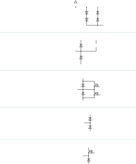
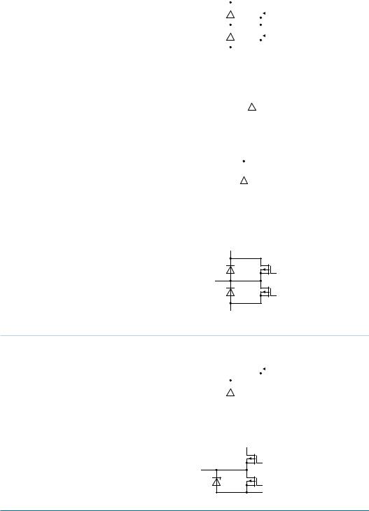
9.Internal circuitry
Table 7. |
Internal circuitry |
|
|
|
||||||||
Pin |
Symbol |
Equivalent circuit |
|
|
|
|||||||
1 |
VSSD(HW) |
1, 16, |
|
|
|
|
|
|
|
|
|
VDDA |
16 |
VSSD(HW) |
|
|
|
|
|
|
|
|
|
||
|
|
|
|
|
|
|||||||
17, 32 |
|
|
|
|
|
|
|
|
|
|
||
17 |
VSSD(HW) |
|
|
|
|
|
|
|
|
|
|
|
|
|
|
|
|
|
|
|
|
|
|
||
32 |
VSSD(HW) |
|
|
|
|
|
|
|
|
|
|
|
|
|
|
|
|
|
|
|
|
|
|
||
|
|
|
|
VSSA |
|
|
|
|
001aad784 |
2 |
IN1P |
|
|
|
3 |
IN1N |
VDDA |
|
|
|
|
|
||
12 |
INREF |
2 kΩ |
|
|
± 20 % |
|
|
||
14 |
2, 15 |
|
|
V/I |
IN2N |
|
|
|
|
15 |
IN2P |
|
48 kΩ |
|
|
|
|
± |
20 % |
|
12 |
|
|
HVPREF |
|
|
|
48 kΩ |
|
|
|
|
± |
20 % |
|
|
2 kΩ |
|
|
|
3, 14 |
± 20 % |
|
V/I |
|
|
|
||
|
|
VSSA |
|
001aad785 |
4 |
DIAG |
|
|
|
|
VDDA |
2.5 V |
|
|
|
|
50 µA |
||
|
|
|
500 Ω |
|
|
4 |
|
± 20 % |
|
|
|
|
|
|
|
|
100 kΩ |
||
|
|
± |
20 % |
|
VSSA |
CGND |
001aaf607
TDA8932B_3 |
© NXP B.V. 21 June 2007. All rights reserved. |
Product data sheet |
Rev. 03— 21 June 2007 |
12 of 48 |
NXP Semiconductors |
|
|
|
|
|
|
|
|
|
|
|
|
|
|
|
|
|
|
|
|
|
|
TDA8932B |
|||||
|
|
|
|
|
|
|
|
|
|
|
|
|
|
|
|
|
|
|
|
|
|
|
Class-D audio amplifier |
|||||
|
Table 7. |
Internal circuitry (Continued) |
|
|
|
|
|
|
|
|
|
|
|
|
|
|
|
|
|
|
||||||||
|
|
|
|
|
|
|
|
|
|
|
|
|
|
|
|
|
|
|
|
|
|
|
|
|
|
|
|
|
|
Pin |
Symbol |
Equivalent circuit |
|
|
|
|
|
|
|
|
|
|
|
|
|
|
|
|
|
|
|||||||
5 |
ENGAGE |
|
|
|
|
|
|
|
|
|
|
|
|
|
|
|
|
|
|
|
|
|
|
|
|
|
|
|
|
|
|
|
VDDA |
|
|
|
|
|
|
|
|
|
|
|
|
2.8 V |
|||||||||||
|
|
|
|
|
|
|
|
|
|
|
|
|
|
|
|
|
|
|
|
|
|
|
|
Iref = 50 μA |
||||
|
|
|
|
|
|
|
|
|
|
|
|
|
|
|
|
|
|
|
|
|
|
|
|
|||||
|
|
|
|
|
|
|
|
|
|
|
|
|
|
|
|
|
|
|
|
2 kΩ |
|
|
|
|
||||
|
|
|
5 |
|
|
|
|
|
|
|
± 20 % |
|
|
|
|
|
|
|||||||||||
|
|
|
|
|
|
|
|
|
|
|
|
|
|
|
|
|
|
|
|
|
|
|
|
|
|
|
|
|
|
|
|
|
|
|
|
|
|
|
|
|
|
|
|
|
100 kΩ |
||||||||||||
|
|
|
|
|
|
|
|
|
|
|
|
|
|
|
± 20 % |
|
|
|
|
|
|
|
|
|||||
|
|
|
|
|
|
|
|
|
|
|
|
|
|
|
|
|
|
|
|
|
|
|
|
|
|
|
|
|
|
|
|
|
|
|
|
|
|
|
|
|
|
|
|
|
|
|
|
|
|
||||||||
|
|
|
|
|
|
|
|
|
|
|
|
|
|
|
|
|
|
|
|
|
|
|
|
|
|
|
|
|
|
|
|
|
VSSA |
CGND |
|||||||||||||||||||||||
|
|
|
|
|
|
|
|
|
|
|
|
|
|
|
|
|
|
|
|
|
|
|
|
001aaf608 |
||||
|
|
|
|
|
|
|
|
|
|
|
|
|
|
|
|
|
|
|
|
|
|
|
|
|
|
|
|
|
6 |
POWERUP |
|
|
|
|
|
|
|
|
|
|
|
|
|
|
|
|
|
|
|
|
|
|
|
|
|
|
|
|
|
|
|
|
|
|
VDDA |
|
|
|
|
|
|
|
|
|
|
|
|
|
|
|
|
|
|
|||
|
|
|
6 |
|
|
|
|
|
|
|
|
|
|
|
|
|
|
|
|
|
|
|
|
|
|
|
||
|
|
|
|
|
|
|
|
|
|
|
|
|
|
|
|
|
|
|
|
|
|
|
|
|
|
|||
|
|
|
|
|
|
|
|
|
|
|
|
|
|
|
|
|
|
|
|
|
|
|
|
|
|
|||
|
|
|
|
|
|
|
|
|
|
|
|
|
|
|
|
|
|
|
|
|
|
|
|
|
|
|
|
|
|
|
|
|
|
|
|
|
|
|
|
|
|
|
|
|
|
|
|
|
|
|
|
|
|
|
|
|
|
VSSA |
CGND |
001aad788 |
7 CGND
VDDA
7
VSSA
001aad789
8 VDDA
8
VSSA
VSSD
001aad790
TDA8932B_3 |
© NXP B.V. 21 June 2007. All rights reserved. |
Product data sheet |
Rev. 03— 21 June 2007 |
13 of 48 |
NXP Semiconductors |
|
|
|
|
|
|
TDA8932B |
||
|
|
|
|
|
|
|
|
Class-D audio amplifier |
|
|
Table 7. |
Internal circuitry (Continued) |
|||||||
|
|
|
|
|
|
|
|
|
|
|
Pin |
Symbol |
Equivalent circuit |
||||||
9 |
VSSA |
|
|
|
|
|
|
|
|
|
|
|
9 |
|
|
|
|
|
VDDA |
|
|
|
|
|
|
|
|
||
|
|
|
|
|
|
|
|
|
|
|
|
|
|
|
|
|
|
|
|
VSSD
001aad791
10 OSCREF
VDDA
 Iref
Iref
10
VSSA 001aad792
11 HVPREF
VDDA
11
VSSA 001aaf604
13 TEST
18 DREF
VDDA
13 |
VSSA |
001aad795 |
VDD
18
VSSD
001aag025
TDA8932B_3 |
© NXP B.V. 21 June 2007. All rights reserved. |
Product data sheet |
Rev. 03— 21 June 2007 |
14 of 48 |
NXP Semiconductors |
|
|
|
|
|
|
|
|
|
|
|
|
|
|
|
|
|
TDA8932B |
||
|
|
|
|
|
|
|
|
|
|
|
|
|
|
|
|
Class-D audio amplifier |
||||
|
Table 7. |
Internal circuitry (Continued) |
||||||||||||||||||
|
|
|
|
|
|
|
|
|
|
|
|
|
|
|
|
|
|
|
|
|
|
Pin |
Symbol |
Equivalent circuit |
|||||||||||||||||
19 |
HVP2 |
|
|
|
|
|
|
|
|
|
|
|
|
|
|
|
|
|
||
|
|
|
|
VDDA |
||||||||||||||||
30 |
HVP1 |
19, 30 |
||||||||||||||||||
|
|
|
|
|
|
|
|
|
|
|
|
|
|
|
|
|||||
|
|
|
|
|
|
|
|
|
|
|
|
|
|
|
|
|
|
|
||
|
|
|
|
|
|
|
|
|
|
|
|
|
|
|
|
|
|
|
||
|
|
|
|
|
|
|
|
|
|
|
|
|
|
|
|
|
|
|
||
|
|
|
|
|
|
|
|
|
|
|
|
|
|
|
|
|
|
|
||
|
|
|
|
|
|
|
|
|
|
|
|
|
|
|
|
|
|
|
||
|
|
|
|
|
|
|
|
|
|
|
|
|
|
|
|
|
|
|||
|
|
|
|
|
|
|
|
|
|
|
|
|
|
|
|
|
|
|
|
|
|
|
|
|
|
|
|
|
|
|
|
|
|
|
|
|
|
|
|
|
|
|
|
|
|
|
|
|
|
|
|
|
|
|
|
|
|
|
|
|
|
|
|
|
|
|
VSSA 001aag026 |
||||||||||||||||
|
|
|
|
|
|
|
|
|
|
|
|
|
|
|
|
|
|
|
|
|
|
20 |
VDDP2 |
20, 29 |
|
|
|
|
|
|
|
|
|
|
|
||||||
|
23 |
VSSP2 |
|
|
|
|
|
|
|
|
|
|
|
|||||||
|
|
|
|
|
|
|
|
|
|
|
|
|
|
|
|
|
||||
|
26 |
VSSP1 |
|
|
|
|
|
|
|
|
|
|
|
|
|
|
|
|
|
|
|
|
|
|
|
|
|
|
|
|
|
|
|
|
|
|
|
||||
29 |
VDDP1 |
23, 26 |
|
|
|
|
|
|
|
|
|
|
|
|||||||
|
|
|
|
|
|
|
|
|
|
|
|
|
|
|||||||
|
|
|
|
|
001aad798 |
|||||||||||||||
|
|
|
|
|
|
|
|
|
|
|
|
|
|
|
|
|
|
|
|
|
21 |
BOOT2 |
|
|
|
|
|
|
|
|
|
|
|
|
|
|
|
|
|
||
|
|
|
21, 28 |
|
|
|
|
|
|
|
|
|
|
|
|
|
|
|||
28 |
BOOT1 |
|||||||||||||||||||
|
|
|
|
|
|
|
|
|
|
|
|
|
|
|
|
|
||||
|
|
|
|
|
|
|
|
|
|
|||||||||||
|
|
|
|
|
|
|
|
|||||||||||||
|
|
|
|
OUT1, OUT2 |
||||||||||||||||
|
|
|
|
|
|
|
|
001aad799 |
||||||||||||
|
|
|
|
|
|
|
|
|
|
|
|
|
|
|
|
|
|
|
|
|
22 |
OUT2 |
|
|
|
|
|
|
|
|
|
|
|
|
|
|
|
|
|
||
|
|
|
|
VDDP1, |
||||||||||||||||
27 |
OUT1 |
|||||||||||||||||||
|
VDDP2 |
|||||||||||||||||||
|
|
|
|
|||||||||||||||||
22, 27
VSSP1,
VSSP2 001aag027
24 |
STAB2 |
|
|
|
|
|
|
|
|
|
|
|
|
|
|
|
|
|
VDDA |
||||||
25 |
STAB1 |
24, 25 |
||||||||||
|
|
|
|
|
|
|
|
|
|
|
|
|
|
|
|
|
|
|
|
|
|
|
|
|
|
|
|
|
|
|
|
|
|
|
|
|
|
|
|
|
|
|
|
|
|
|
|
|
|
|
|
|
|
|
|
|
|
|
|
|
|
|
|
|
|
|
|
VSSP1, |
|||||||||
|
|
|
VSSP2 001aag028 |
|||||||||
|
|
|
|
|
|
|
|
|
|
|
|
|
31 |
OSCIO |
|
|
|
|
|
|
|
|
|
|
|
|
|
|
|
|
|
DREF |
||||||
31
VSSD
001aag029
TDA8932B_3 |
© NXP B.V. 21 June 2007. All rights reserved. |
Product data sheet |
Rev. 03— 21 June 2007 |
15 of 48 |
 Loading...