

Page 1
UM10340_5
TFA9879 digital input mono Class-D amplifier demo PCB
Rev. 05 — 30 aug. 2011 User manual
Document information
Info Content
Keywords Class-D amplifier, Digital input, High efficiency, Filter free
Abstract This User Manual describes the TFA9879 digital input mono Class-D
demonstration PCB based on NXP Semiconductors’ TFA9879 filter-free
mono BTL Class-D audio amplifier device. The TFA9879 device is
intended for portable applications that support a digital output, which is
less sensitive to external RF fields. The low power consumption will
increase the battery life and an excellent audio performance with high
PSRR is achieved by the integrated feedback loop.
Furthermore the device is very robust due to the integrated protections
like OCP, OTP and several input protections.
The demonstration PCB is designed to operate from a single supply with
a wide supply voltage range of 2.5V…5.5V delivering an output power up
to 1.6W
RMS
in 8Ω BTL or 2.7W
RMS
4Ω BTL. The application PCB area for
the TFA9879 is very small because only three external components are
required. The demo board is EMC compliant and contains 15kV ESD
protections at the speaker output.
Page 2

NXP Semiconductors
UM10340_5
TFA9879 demonstration PCB
<DOC ID>
© NXP B.V. 2011. All rights reserved.
User manual Rev. 05 — 30 aug. 2011 2 of 20
Con
tact information
For additional information, please visit: http://www.nxp.com
For sales office addresses, please send an email to: salesaddresses@nxp.com
Revision history
Rev Date Description
1 20090227 Initial version
2 20090806 Main PCB updated to revision 2 and WLCSP translation PCB replaced by HVQFN24
translation PCB
3 20090911 Translation PCB updated to revision 3 for TFA9879 (N1B2/N1C) engineering samples
4 20091210 Main PCB and translation PCB updated to revision R3 for the final TFA8979 (N1C)
samples
5 20110830 Main PCB Revision 4
Page 3

NXP Semiconductors
UM10340_5
TFA9879 demonstration PCB
© NXP B.V. 2011. All rights reserved.
User manual Rev. 05 — 30 aug. 2011 3 of 20
1. Introduction
This User Manual describes the TFA9879 digital input mono Class-D amplifier
demonstration PCB based on NXP Semiconductors’ TFA9879HN device. Extension “HN”
is referring to the HVQFN24 package dedicated for reflow soldering.
The TFA9879 demonstration PCB is designed in such a way that it is easy to operate the
TFA9879 device for demonstration purposes and for validation. Therefore the
demonstration PCB facilitates the following circuitry (see Figure 1):
• TFA9879 Class-D amplifier requires only three external components that are
stuffed at a translation PCB.
• Analog to digital converter (ADC + clock generator, I2S format, fs = 48kHz) to
drive the speaker via the Class-D amplifier with analog signals.
• 3.3V buck boost converter (DCDC) for the ADC and I2C pull-up voltage.
• 1.8V linear regulator for the digital core of the TFA9879.
• External 15kV ESD protection at amplifier output.
Figure 1: Block diagram demonstration PCB
Demonstration PCB
Speaker
TFA9879
OUTA
Class-D
Class-D
Volume control
5-band parametric EQ
DRC
Bass-treble control
High-pass filter
Power limiter
PWM
modulator
PLL
I2C
control
interface
Interface
I2S input 1
I2S input 2
I2C control input
Protections
OCP
OTP
Mono speaker driver
Digital processor
Digital
audio
receiver
MUX
Input
protections
OFP
UFP
IBP
VDDP VDDD
Supply 2.5V...5.5V
Feedback
loop
Feedback
loop
OUTB
C
STABA
STABA
1.8V
Address select
A/D converter
3.3V
Analog input
Class-D amplifier
1.8V linear
regulator
3.3V buck boost
converter
12.29 MHz
Left
ADC
SYSCLK
Right
LRCK1
SCK1
SDI1
3.3V
V
P
SDA
S1
1.8V
1.8V
LRCK2
SCK2
SDI2
S3
S4
S2
Shutdown
DCDC
Shutdown
LDO
Shutdown
ADC
GNDPGNDD
GND
S5
SCL
ADSEL1
ADSEL2
Page 4

NXP Semiconductors
UM10340_5
TFA9879 demonstration PCB
© NXP B.V. 2011. All rights reserved.
User manual Rev. 05 — 30 aug. 2011 4 of 20
The necessary information is given for a quick start-up of the demonstration PCB (see
paragraph 2). Paragraph 3 shows the results of the audio characterization and the
schematic, BOM and layout is provided in paragraph 4, 5 and 6.
The TFA9879 device has the following functions / features:
General
• Wide supply voltage range 2.5V…5.5V
• Two digital inputs (I2S and PCM/IOM2 formats, 1.8V and 3.3V tolerant) which
are less sensitive to external RF fields
• Internal Phase-Locked Loop (PLL) requiring no system clock
• High efficiency of 92% and low power consumption
• Closed loop amplifier resulting in excellent audio performance:
• PSRR = -76 dB
• S/N = -95dB (A-weighted)
• THD+N = 0.015% at 100mW
RMS
• High power capability:
• 2.7 W
RMS
in 4Ω BTL at 5V
• 1.6 W
RMS
in 8Ω BTL at 5V
• Protections including diagnostic via I2C
• I2S and PCM/IOM2 input protections
• Under Frequency Protection (UFP)
• Over Frequency Protection (OFP)
• Invalid Bit clock Protection (IBP)
• Over Current Protection (OCP)
• Over Temperature Protection (OTP)
• HVQFN24 package
DSP
• Volume control (-70dB to +24dB)
• 5-band parametric equalizer
• Dynamic Range Compression
• Bass-treble control (-18dB to +18dB)
• High-pass filter
• Power limiter (0dB to –124dB)
• Zero crossing detect
Page 5
NXP Semiconductors
UM10340_5
TFA9879 demonstration PCB
© NXP B.V. 2011. All rights reserved.
User manual Rev. 05 — 30 aug. 2011 5 of 20
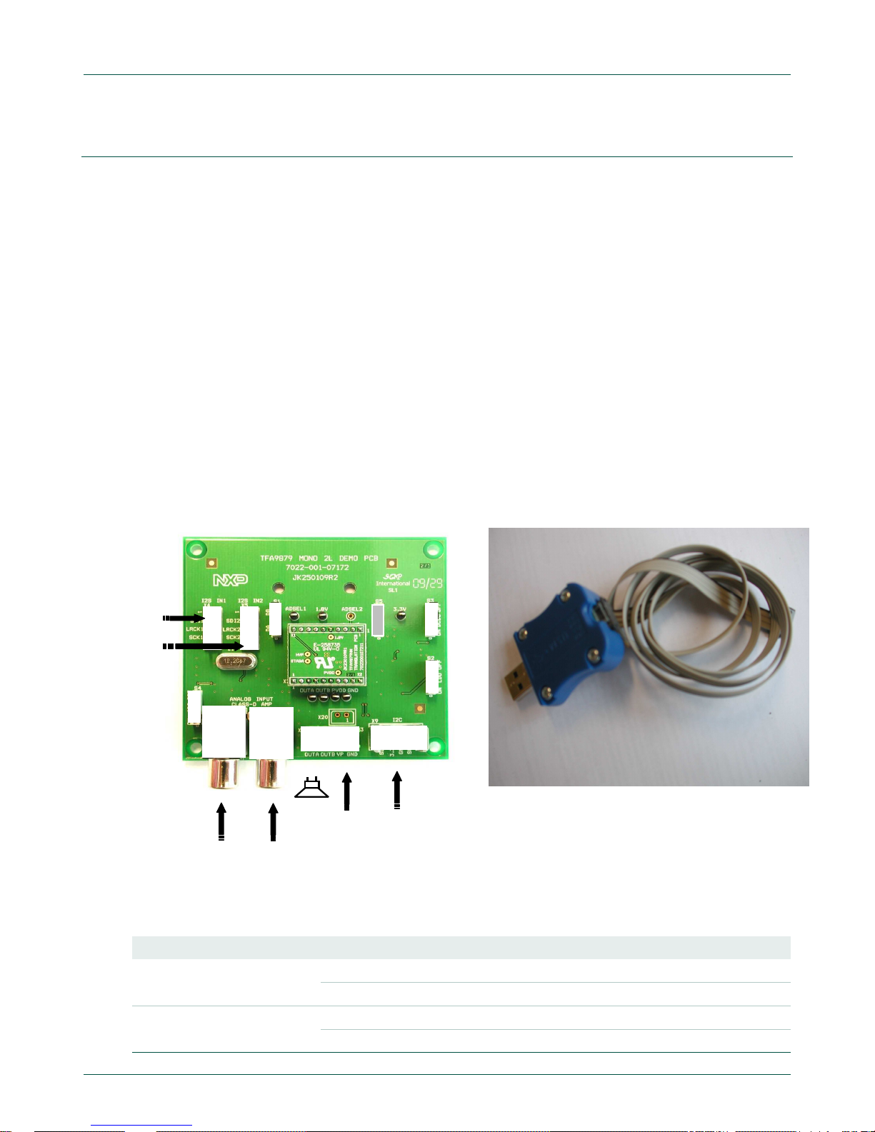
2. Setup demonstration PCB
2.1 Hardware setup
Figure 2 is showing the hardware setup of the TFA9879 mono demonstration PCB with
screw terminals for connecting the power supply (X3) and the speaker cables (X7).
The speaker can be driven by the Class-D amplifier with:
• A digital audio signal via the headers X4 (I2S input 1) or X5 (I2S input 2);
• An analog stereo audio signal via the RCA Jacks X14 and X11 (I2S input 2).
Remark: Default the ADC is connected to the I2S input 2 of the TFA9879 via R35, R36
and R37 (10R, see schematic in paragraph 4). These 10R resistors must be removed
from the PCB when driving I2S via X5.
The USM interface (USB to I2C converter) including the 4-wire flat cable, which are
provided with the board, should be connected between demonstration PCB (connector
X9) and USM interface. The USB port should be connected to the PC.
Important remark: First install the GUI software (see paragraph 2.2.1), which includes the
USB driver, before connecting the USM interface to the PC.
+ OUT - Supply I2C
input
Right Left
Analog Class
-D input
S3
X7 X3
X14 X11
S2
S4
S1
X4 X5
X9
Digital
Class-
D input
I2S input 1
I2S input 2
S5
3
Figure 2: Setup demonstration PCB Figure 3: USM interface
Table 1. Input/output connector assignment
REF TYPE
Pin Label
Description
X3 Terminal block, screw
1 GND Ground
2 V
P
Positive supply input (2.5V…5.5V)
X4 Header, double row
1, 2, 9, 10
Not connected
3 SDI1
Data input 1
Page 6
NXP Semiconductors
UM10340_5
TFA9879 demonstration PCB
© NXP B.V. 2011. All rights reserved.
User manual Rev. 05 — 30 aug. 2011 6 of 20
REF TYPE
Pin Label
Description
4, 6, 8
GND Ground
5 LRCK1
Word clock input 1
7 SCK1
Bit clock input 1
X5
Header, double row
1, 2, 9, 10
Not connected
3 SDI2
Data input 2
4, 6, 8
GND Ground
5 LRCK2
Word clock input 2
7 SCK2
Bit clock input 2
X7 Terminal block, screw
1
OUTB
PWM output B (negative output)
2 OUTA
PWM output A (positive output)
X9 Stocko header
1
SCL Serial clock input
2 GND Ground
3 3.3V 3.3V supply output
4 SDA Serial data I/O
X11 RCA Jack
1
Left Left analog input to drive Class
-
D amplifier
2 GND Ground
X14 RCA Jack
1
Right
Right analog input to drive Class
-
D am
plifier
2 GND Ground
2.1.1 PCB switch settings
PCB switch S1 and S5 are incorporated to select between the I2C addresses.
I2C address select
S5 S1 address
0 0 D8
0 1 DA
1 0 DC
1 1 DE
S2, S3 and S4 are incorporated to power-down respectively the 1.8V LDO, the DCDC
converter and the ADC converter if required. The LDO and the DCDC converter must be
turned on to operate the TFA9879. The ADC might be turned off when not used.
2.1.2 Digital input formats
Below digital formats are supported by the TFA9879 device:
I2S formats (fs = 8kHz to 96kHz)
• Philips standard I2S
• Japanese I2S MSB-justified
• Sony I2S LSB-justified
PCM/IOM2 formats (fs = 8kHz)
• Long frame sync
• Short frame sync
Page 7

NXP Semiconductors
UM10340_5
TFA9879 demonstration PCB
© NXP B.V. 2011. All rights reserved.
User manual Rev. 05 — 30 aug. 2011 7 of 20
L
E
R
DC
2.1.3 Speaker dummy load
The TFA9879 is a filter-free Class-D amplifier that will directly drive the loudspeaker. For
realistic measurement at a filter-free Class-D amplifier a dummy load, consisting out of a
resistor (RDC) in series with an inductor (LE), should replace the loudspeaker. The resistor
represents the loudspeaker dc resistance and the inductor (LE) represents the
loudspeaker coil.
Figure 4: Simplified loudspeaker model
Measurement at the demonstration PCB are performed with resistor of RDC = 8Ω, LE =
44µH or RDC = 4Ω, LE = 20µH. But inductor values between respectively 15µH and 60µH
are suitable (saturation current >1.5A) for measurements as well.
Page 8

NXP Semiconductors
UM10340_5
TFA9879 demonstration PCB
© NXP B.V. 2011. All rights reserved.
User manual Rev. 05 — 30 aug. 2011 8 of 20
2.2 Software setup (GUI)
The TFA9879 is controlled via I2C. The Graphic User Interface (GUI) software (including
USM drivers), which are supplied by the demonstration PCB, enable easy control of the
I2C registers in the TFA9879.
Important remark: First install the GUI software, which includes the USM drivers, before
connecting the USM interface to the PC.
2.2.1 Installing software
Follow below steps for a proper installation of the I2C GUI and USM drivers:
1. Run the installation file (TFA9879_4_2_0.exe or higher) on a Windows XP operating
system (or higher) and follow the installation procedure. The GUI will start
automatically after installation.
2. Exit the I2C GUI program.
3. Connect the USM interface to the PC.
4. Windows will automatically detect the USM interface and a hardware wizard helps to
install the software. Select the option “install the software automatically”. Furthermore
a warning about Windows Logo testing might appear. Click on “Continue Anyway”
and installation of the USM interface will be finalized.
5. Connect the I2C cable to the demonstration PCB and turn-on the power supply. S2
and S3 at the demonstration PCB should be in the “ON” position. Start-up the I2C
GUI program:
6. Select from the menu respectively I2C Config Detect and wait until “USM”
appears in the interface box. Close this window.
Figure 6: I2C menu
Figure 5: Warning
Page 9

NXP Semiconductors
UM10340_5
TFA9879 demonstration PCB
© NXP B.V. 2011. All rights reserved.
User manual Rev. 05 — 30 aug. 2011 9 of 20
7. Select a device address (D8, DA, DC or DE) from the GUI (top right side).
The installation of I2C GUI is finalized and the indicator of the I2C communication
should be green.
Figure 7: GUI communication
If the indication is still red the following should be checked:
• An equal device address should be selected (D8, DA, DC or DE) in GUI and
demonstration PCB (S1/S5)
• Connection of the USM interface
• S2 and S3 should be in the “ON” position
2.3 Settings to play audio
The following settings are required to play audio via the analog RCA-jack inputs.
Hardware settings:
• Turn on ADC, S4 in “ON” position (S2 and S3 also in “ON” position)
• Apply Left and Right audio signal to the RCA-jack inputs (X11, X14)
Page 10

NXP Semiconductors
UM10340_5
TFA9879 demonstration PCB
© NXP B.V. 2011. All rights reserved.
User manual Rev. 05 — 30 aug. 2011 10 of 20
GUI settings:
• Select Powerup
• Select input 2
• Select Operating Mode “On”
• Increase volume (for example to 0dB)
Figure 8: GUI settings to play audio
Page 11

NXP Semiconductors
UM10340_5
TFA9879 demonstration PCB
© NXP B.V. 2011. All rights reserved.
User manual Rev. 05 — 30 aug. 2011 11 of 20
3. Performance characterization TFA9879HN
Table below shows the measured performance figures of the TFA9879HN demonstration
PCB. Digital I2S input signal is applied to connector X4 and the audio analyzer is
connected via an AUX-0025 passive filter from Audio Precision to the PWM outputs
(OUTA, OUTB).
VP = 3.7 V, 8 Ω + 44µH, fi = 1 kHz, I2S format, fS = 48kHz, T
amb
= 25 °C unless specified
otherwise.
Table 2. Performance figures
Symbol
Parameters
Conditions / Notes
Min Typ Max Unit
Vp
Supply voltage
2.5
1
5.5
1
V
Po
RMS output power
Clip control on
3
(off4)
RL = 8 Ω; Vp = 3.7 V
THD+N = 10 %
760 (870)
mW
THD+N = 1 %
590 (720)
mW
RL = 8 Ω; Vp = 4.2 V
THD+N = 10 %
970 (1120)
mW
THD+N = 1 %
770 (940)
mW
RL = 8 Ω; Vp = 5.0 V
THD+N = 10%
1.4 (1.6)
W
THD+N = 1%
1.1(1.3)
W
RL = 4 Ω; Vp = 3.7 V
THD+N = 10%
1.3 (1.5)
W
THD+N = 1%
1.0 (1.2)
W
RL = 4 Ω; Vp = 4.2 V
THD+N = 10%
1.7 (2.0)
W
THD+N = 1%
1.3 (1.6)
W
RL = 4 Ω; Vp = 5.0 V
THD+N = 10%
2.4 (2.7)
W
THD+N = 1%
1.9 (2.2)
W
THD+N
Total Harmonic Distor
tion
and Noise
RL = 8 Ω; P
o
= 100 mW, AES17 brick wall filter 20 kHz
0.015 %
RL = 4 Ω, Po = 100 mW, AES17 brick wall filter 20 kHz
0.025 %
η
Efficiency
TFA9879
4
Vp = 3.7V, Rl = 4Ω, Po = 1.3W
Vp = 3.7V, Rl = 8Ω, Po = 0.76W
88
92
%
%
Vp = 5V, Rl = 4Ω, Po = 2.4W
Vp = 5V, Rl = 8Ω, Po = 1.4W
88
91
%
%
SEN Input Sensitivity
PO
= 100 mW, Volume 0dB
-13 dBFS
V
n(o)
Noise output voltage
Vp
= 5 V, Soft mute, A
-
weighted
58
µ
V
S/N Signal to Noise ratio
A-
weighted w.r.t. V
o
= 3.5 V
RMS
-95 dB
BW Band Width
+/- 1 dB @ Po = 100mW
10…20.000
Hz
PSRR
Power Supply Rejection
Ratio
V
ripple
= 200mVrms, f = 217Hz, no input signal
-76 dB
Page 12

NXP Semiconductors
UM10340_5
TFA9879 demonstration PCB
© NXP B.V. 2011. All rights reserved.
User manual Rev. 05 — 30 aug. 2011 12 of 20
Symbol
Parameters
Conditions / Notes
Min Typ Max Unit
IP Supply current total
application
Power down mode
LDO off, DCDC off, ADC off
34
µ
A
LDO on, DCDC
on, ADC on
29 mA
Off mode
LDO on, DCDC off, ADC off
2.2 mA
LDO on, DCDC on, ADC on
32 mA
Amplifier on mode, no load
Hard/soft mute, LDO on, DCDC off, ADC off
7 mA
Hard/soft mute, LDO on, DCDC on, ADC on
36 mA
[1] It is not recommended to operate the device at the supply boundaries unless the supply is regulated well.
[2] Clip control on results in smooth clipping.
[3] Clip control off results in maximum output power.
[4] The efficiency of the total application is slightly worse due to the power dissipation in LDO and DCDC
converter.
Page 13

NXP Semiconductors
UM10340_5
TFA9879 demonstration PCB
© NXP B.V. 2011. All rights reserved.
User manual Rev. 05 — 30 aug. 2011 13 of 20
4. Schematics
Page 14

NXP Semiconductors
UM10340_5
TFA9879 demonstration PCB
© NXP B.V. 2011. All rights reserved.
User manual Rev. 05 — 30 aug. 2011 14 of 20
Page 15

NXP Semiconductors
UM10340_5
TFA9879 demonstration PCB
© NXP B.V. 2011. All rights reserved.
User manual Rev. 05 — 30 aug. 2011 15 of 20
5. Bill Of Materials
5.1 Main PCB 7022-001-07164
Item Qty Reference
Part Foot print
1 1 A1 ADP3336
MSOP8
2 1 A2 LTC3440EMS
MSOP10
3 1 A3 UDA1361TS
SSO
P16-SOT369
-1
4 2 C1,C21
10n C0603
5 4 C2,C9,C11
,C14 10uF
C0603
6 4 C3,C12,C17,C20
1u
C0603
7 5 C4,C5,C6,C7,C10
1n
C0603
8 1 C8 150pF
C0603
9 1 C22 100n
F C0603
10 1 C13 47uF
C0805
11 2 C15,C16
1.5nF
C0603
12 1 C23 10pF
C0603
13 1 C24 82pF
C0603
14 1 D1 74HCU04D
SO14
15 4 L1,L3,L4,L5
BLM18EG221SN1
L0603
16 1 L2 10uH
LPS4018
17 4 R1,R11,R29,R32
470K
R0603
18 4 R2,R7,R9,R38
10K R0603
19 1 R3 82K R0603
20 1 R4 150K
R0603
21 2 R5,R6
0
R0603
22 1 R8 4E7 R0603
23 7 R10,R13,
R19,R33,R35,R36,R37
10
R0603
24 1 R12 270K
R0603
25 1 R14 15K R0603
26 1 R17 160K
R0805
27 1 R18 56K R0603
28 2 R20,R25
,R30,R34
1K R0603
29 2 R39
8.2K
R0603
30 5 S1,S2,S3,S4,S5
Secme PCB Jumper Switch 3P
31 2 V1,V2
SL04
DO219AB
32 1 V3 IP43
03CX4/LF
WLCSP4
33 2 X1,X2
Vertical Receptable Single Row 2mm 10p
34 2 X3,X7
Vertical PCB Mounted Screw Terminal small 2P
35 2 X4,X5
Header Straight Pins Double Row / 10p
36 8 X6,X8,X10,X13,X15,X16,X17,X18
Isolated Testpin
37 1 X9 Stocko Header S
traight Pins 4p
38 2 X11,X14
Phono Conn Black WBTOR
-1
39 1 X20 Header 2P Pitch2.5MM
40 1 Z1 12.288Mhz
CRYSTAL HC
-49-S
Page 16

NXP Semiconductors
UM10340_5
TFA9879 demonstration PCB
© NXP B.V. 2011. All rights reserved.
User manual Rev. 05 — 30 aug. 2011 16 of 20
5.2 Translation PCB 7022-001-07203
Item Qty Reference Part Foot print
1 1 A1 TFA9879HN HVQFN24-SOT616-1
2 1 C1 10u C0603
3 2 C2,C3 100n C0402
4 2 X1,X2 Header Single Row / 10p 2mm
5 4 X4,X5,X6 SMD-TESTPAD-1MM5
6 1 R1 0 Ω R0402
Page 17

NXP Semiconductors
UM10340_5
TFA9879 demonstration PCB
© NXP B.V. 2011. All rights reserved.
User manual Rev. 05 — 30 aug. 2011 17 of 20
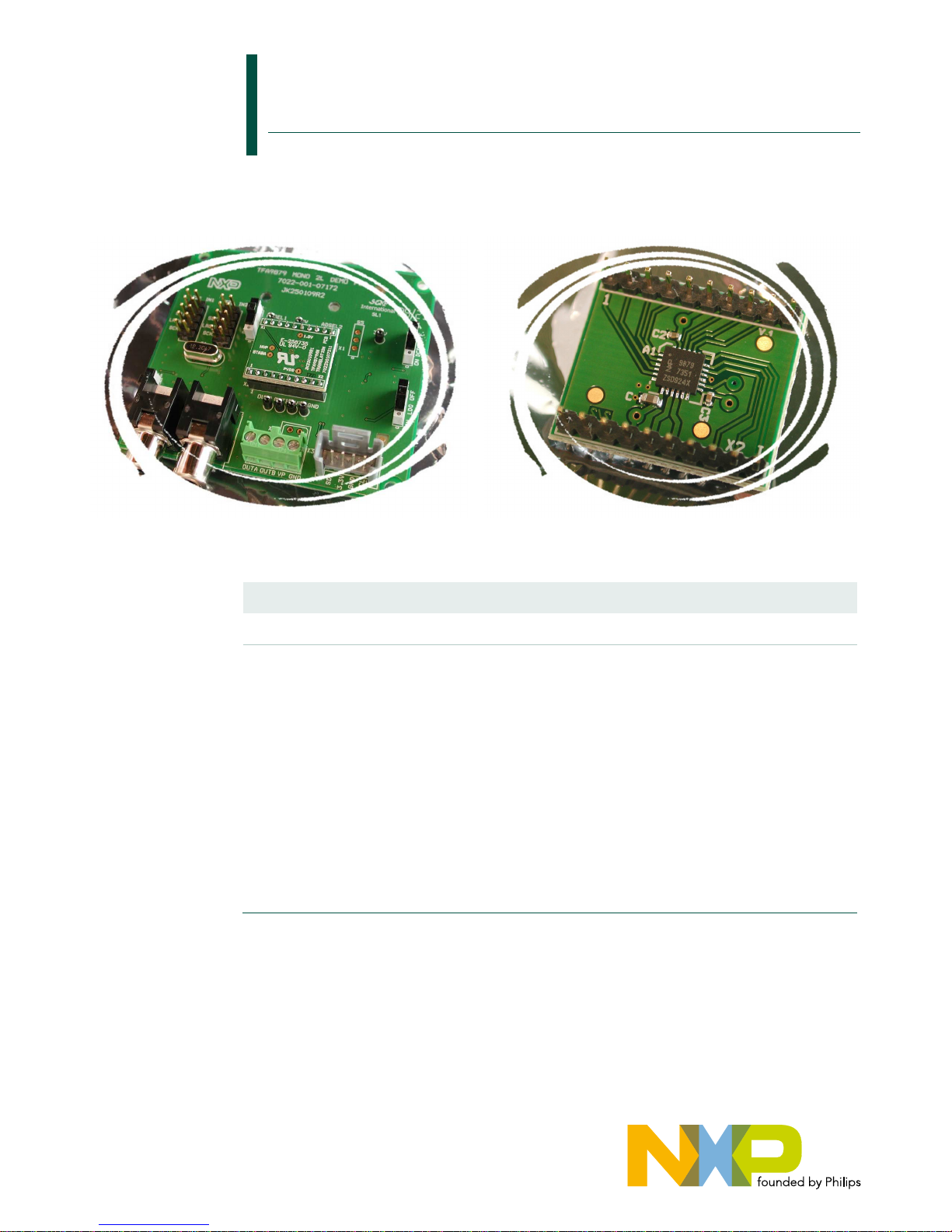
6. PCB layout
6.1 Main PCB 7022-001-07174
Two layer PCB (74mm x 65mm), 35µm copper and FR4 base material.
Figure 9 Copper and silkscreen top layer (top view)
Figure 10: Copper and silkscreen top layer (top view)
Page 18

NXP Semiconductors
UM10340_5
TFA9879 demonstration PCB
© NXP B.V. 2011. All rights reserved.
User manual Rev. 05 — 30 aug. 2011 18 of 20
6.2 Translation PCB 7022-001-07213
Two layer PCB (20mm x 18mm), 35µm copper and FR4 base material.
Figure 9: Copper and silkscreen top layer (top view) Figure 10: Copper and silkscreen bottom layer (top view)
Page 19

NXP Semiconductors
UM10340_5
TFA9879 demonstration PCB
<DOC ID>
© NXP B.V. 2011. All rights reserved.
User manual Rev. 05 — 30 aug. 2011 19 of 20
7. Legal information
7.1 Definitions
Draft — The document is a draft version only. The content is still under
internal review and subject to formal approval, which may result in
modifications or additions. NXP Semiconductors does not give any
representations or warranties as to the accuracy or completeness of
information included herein and shall have no liability for the consequences
of use of such information.
7.2 Disclaimers
General — Information in this document is believed to be accurate and
reliable. However, NXP Semiconductors does not give any representations
or warranties, expressed or implied, as to the accuracy or completeness of
such information and shall have no liability for the consequences of use of
such information.
Right to make changes — NXP Semiconductors reserves the right to make
changes to information published in this document, including without
limitation specifications and product descriptions, at any time and without
notice. This document supersedes and replaces all information supplied prior
to the publication hereof.
Suitability for use — NXP Semiconductors products are not designed,
authorized or warranted to be suitable for use in medical, military, aircraft,
space or life support equipment, nor in applications where failure or
malfunction of a NXP Semiconductors product can reasonably be expected
to result in personal injury, death or severe property or environmental
damage. NXP Semiconductors accepts no liability for inclusion and/or use of
NXP Semiconductors products in such equipment or applications and
therefore such inclusion and/or use is for the customer’s own risk.
Applications — Applications that are described herein for any of these
products are for illustrative purposes only. NXP Semiconductors makes no
representation or warranty that such applications will be suitable for the
specified use without further testing or modification.
7.3 Trademarks
Notice: All referenced brands, product names, service names and
trademarks are property of their respective owners.
Page 20

NXP Semiconductors
UM10340_5
TFA9879 demonstration PCB
© NXP B.V. 2011. All rights reserved.
User manual Rev. 05 — 30 aug. 2011 20 of 20
8. Contents
1.
Introduction ......................................................... 3
2.
Setup demonstration PCB .................................. 5
2.1
Hardware setup .................................................. 5
2.1.1
PCB switch settings ........................................... 6
2.1.2
Digital input formats ........................................... 6
2.1.3
Speaker dummy load ......................................... 7
2.2
Software setup (GUI) ......................................... 8
2.2.1
Installing software .............................................. 8
2.3
Settings to play audio ......................................... 9
3.
Performance characterization TFA9879HN ..... 11
4.
Schematics ........................................................ 13
5.
Bill Of Materials ................................................. 15
5.1
Main PCB 7022-001-07164 .............................. 15
5.2
Translation PCB 7022-001-07203 .................... 16
6.
PCB layout ......................................................... 17
6.1
Main PCB 7022-001-07174 .............................. 17
Figure 10: Copper and silkscreen top layer (top view) ...... 17
6.2
Translation PCB 7022-001-07213 .................... 18
7.
Legal information .............................................. 19
7.1
Definitions ......................................................... 19
7.2
Disclaimers ....................................................... 19
7.3
Trademarks ...................................................... 19
8.
Contents ............................................................. 20
 Loading...