

Page 1

UM10204
I2C-bus specification and user manual
Rev. 5 — 9 October 2012 User manual
Document information
Info Content
Keywords I2C, I2C-bus, Standard-mode, Fast-mode, Fast-mode Plus, Fm+,
Ultra Fast-mode, UFm, High Speed, Hs, inter-IC, SDA, SCL, USDA, USCL
Abstract Philips Semiconductors (now NXP Semiconductors) developed a simple
bidirectional 2-wire bus for efficient inter-IC control. This bus is called the
Inter-IC or I
2
C-bus. Only two bus lines are required: a serial data line
(SDA) and a serial clock line (SCL). Serial, 8-bit oriented, bidirectional
data transfers can be made at up to 100 kbit/s in the Standard-mode, up to
400 kbit/s in the Fast-mode, up to 1 Mbit/s in the Fast-mode Plus (Fm+), or
up to 3.4 Mbit/s in the High-speed mode . The Ultra Fast-mode is a
uni-directional mode with data transfers of up to 5 Mbit/s.
Page 2

UM10204 All information provided in this document is subject to legal disclaimers. © NXP B.V. 2012. All rights reserved.
User manual Rev. 5 — 9 October 2012 2 of 64
Contact information
For more information, please visit: http://www.nxp.com
For sales office addresses, please send an email to: salesaddresses@nxp.com
NXP Semiconductors
UM10204
I2C-bus specification and user manual
Revision history
Rev Date Description
v.5 20121009 User manual; fifth release
Modifications: • Section 3.1.7 “Clock synchronization”, first paragraph, first sentence changed from “idle bus”
to “free bus”
• Section 3.1.8 “Arbitration”, third paragraph, second sentence changed from “the bus is idle”
to “the bus is free”
• Section 3.1.12 “Reserved addresses”:
– Table 3 “Reserved addresses”, slave address 11111XX: R/W bit changed from “X” to “1”;
description changed from “reserved for future purposes” to “device ID”
– deleted (old) third paragraph
• Section 3.1.17 “Device ID”:
– in numbered list following second paragraph: “START command” changed to “START
condition”
– in numbered list following second paragraph: “STOP command” changed to “STOP condition”
– in Remark paragraph: “NACK command” changed to “NACK”
– Table 4 “
Assigned manufacturer IDs” updated
• Section 3.2.8 “10-bit addressing”:
– fifth paragraph (bullet item): “NA1” changed to “W
” in third sentence; deleted “(NA2)” from
fourth sentence
– Figure 29 “A master-transmitter addresses a slave-receiver with a 10-bit address” modified
• Section 3.2.9 “Reserved addresses in UFm”: deleted (old) third paragraph
• Section 7.2.1 “Reduced f
SCL
”, third paragraph corrected from “30 % to 30 %, or 70 % to 70 %”
to “30 % to 70 %, or 70 % to 30 %”
v.4 20120213 User manual Rev. 4
v.3 20070619 Many of today’s applications require longer buses and/or faster speeds. Fast-mode Plus was
introduced to meet this need by increasing drive strength by as much as 10× and increasing the data
rate to 1 Mbit/s while maintaining downward compatibility to Fast-mode and Standard-mode speeds
and software commands.
v2.1 2000 Version 2.1 of the I
2
C-bus specification
v2.0 1998 The I
2
C-bus has become a de facto world standard that is now implemented in over 1000 different ICs
and licensed to more than 50 companies. Many of today’s applications, however, require higher bus
speeds and lower supply voltages. This updated version of the I
2
C-bus specification meets those
requirements.
v1.0 1992 Version 1.0 of the I
2
C-bus specification
Original 1982 first release
Page 3

UM10204 All information provided in this document is subject to legal disclaimers. © NXP B.V. 2012. All rights reserved.
User manual Rev. 5 — 9 October 2012 3 of 64
NXP Semiconductors
UM10204
I2C-bus specification and user manual
1. Introduction
The I2C-bus is a de facto world standard that is now implemented in over 1000 different
ICs manufactured by more than 50 companies. Additionally, the versatile I
2
C-bus is used
in various control architectures such as System Management Bus (SMBus), Power
Management Bus (PMBus), Intelligent Platform Management Interface (IPMI), Display
Data Channel (DDC) and Advanced Telecom Computing Architecture (ATCA).
This document assists device and system designers to underst and how the I
2
C-bus works
and implement a working application. Various operating modes are described. It contains
a comprehensive introduction to the I
2
C-bus data transfer, handshaking and bus
arbitration schemes. Detailed sections cover the timing and electrica l specifications for the
I
2
C-bus in each of its operating modes.
Designers of I
2
C-compatible chips should use this document as a reference and ensure
that new devices meet all limits specified in this document. Designers of systems that
include I
2
C devices should review this document and also refer to individual component
data sheets.
2. I2C-bus features
In consumer electronics, telecommunications and industrial electronics, there are often
many similarities between seemingly unrelated designs. For example, nearly every
system includes:
• Some intelligent control, usually a single-chip microcontroller
• General-purpose circuits like LCD and LED drivers, remote I/O ports, RAM,
EEPROM, real-time clocks or A/D and D/A converters
• Application-oriented circuits such as digital tuning and signal processing circuits for
radio and video systems, temperature sensors, and smart cards
To exploit these similarities to the benefit of both systems designers and equipment
manufacturers, as well as to maximize hardware efficiency and circuit simplicity, Philips
Semiconductors (now NXP Semiconductors) developed a simple bidirectional 2-wire bus
for efficient inter-IC control. This bus is called the Inter IC or I
2
C-bus. All I2C-bus
compatible devices incorporate an on-chip interface which allows them to communicate
directly with each other via the I
2
C-bus. This design concept solves the many interfacing
problems encountered when designing digital control circuits.
Here are some of the features of the I
2
C-bus:
• Only two bus lines are required; a serial data line (SDA) and a serial clock line (SCL).
• Each device connected to the bus is software addressable by a unique address and
simple master/slave relationships exist at all times; masters can operate as
master-transmitters or as master-receivers.
• It is a true multi-master bus including collision detection and arbitration to prevent data
corruption if two or more masters simultaneously initiate data transfer.
• Serial, 8-bit oriented, bidirectional data transfers can be made at up to 100 kbit/s in
the Standard-mode, up to 400 kbit/s in the Fast-mode, up to 1 Mbit/s in Fast-mode
Plus, or up to 3.4 Mbit/s in the High-speed mode.
Page 4
UM10204 All information provided in this document is subject to legal disclaimers. © NXP B.V. 2012. All rights reserved.
User manual Rev. 5 — 9 October 2012 4 of 64
NXP Semiconductors
UM10204
I2C-bus specification and user manual
• Serial, 8-bit oriented, unidirectional data transfers up to 5 Mbit/s in Ultra Fast-mode
• On-chip filtering rejects spikes on the bus data line to preserve data integrity.
• The number of ICs that can be connected to the same bus is limited only by a
maximum bus capacitance. More capacitance may be allowed under some
conditions. Refer to Section 7.2
.
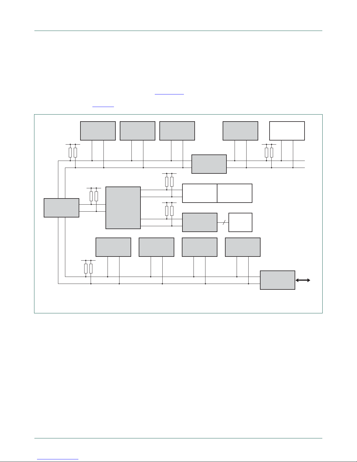
Figure 1
shows an example of I2C-bus applications.
2.1 Designer benefits
I2C-bus compatible ICs allow a system design to progress rapidly directly from a
functional block diagram to a prototype. Moreover, since they ‘clip’ directly onto the
I
2
C-bus without any additional external interfacing, they allow a prototype system to be
modified or upgraded simply by ‘clipping’ or ‘unclipping’ ICs to or from the bus.
Here are some of the features of I
2
C-bus compatible ICs that are particularly attractive to
designers:
• Functional blocks on the block diagram correspond with the actual ICs; designs
proceed rapidly from block diagram to final schematic.
• No need to design bus interfaces because the I
2
C-bus interface is already integrated
on-chip.
Fig 1. Example of I2C-bus applications
I2C
A/D or D/A
Converters
I2C
General Purpose
I/O Expanders
I
2
C
LED Controllers
V
DD4
I2C
Repeaters/
Hubs/Extenders
I2C
DIP Switches
V
DD5
I2C
Slave
V
DD0
V
DD1
PCA9541
I
2
C
Master Selector/
Demux
I2C
Multiplexers
and Switches
V
DD2
I2C Port
via HW or
Bit Banging
I2C
Bus Controllers
MCUs
8
MCUs
I2C
Serial EEPROMs
LCD Drivers
(with I
2
C)
I
2
C
Real Time Clock/
Calendars
V
DD3
I2C
Temperature
Sensors
Bridges
(with I
2
C)
SPI
UART
USB
002aac858
Page 5

UM10204 All information provided in this document is subject to legal disclaimers. © NXP B.V. 2012. All rights reserved.
User manual Rev. 5 — 9 October 2012 5 of 64
NXP Semiconductors
UM10204
I2C-bus specification and user manual
• Integrated addressing and data-transfer protocol allow systems to be completely
software-defined.
• The same IC types can often be used in many different applications.
• Design-time reduces as designers quickly become familiar with the frequently used
functional blocks represented by I
2
C-bus compatible ICs.
• ICs can be added to or removed from a system without affecting any other circuits on
the bus.
• Fault diagnosis and debugging are simple; malfunctions can be immediately traced.
• Software development time can be reduced by assembling a library of reusable
software modules.
In addition to these advantages, the CMOS ICs in the I
2
C-bus compatible range offer
designers special features which are particularly attractive for portab le equipment and
battery-backed systems.
They all have:
• Extremely low current consumption
• High noise immunity
• Wide supply voltage range
• Wide operating temperature range.
2.2 Manufacturer benefits
I2C-bus compatible ICs not only assist designers, they also give a wide range of benefits
to equipment manufacturers because:
• The simple 2-wire serial I
2
C-bus minimizes interconnections so ICs have fewer pins
and there are not so many PCB tracks; result — smaller and less expensive PCBs.
• The completely integrated I
2
C-bus protocol eliminates the need for address decoders
and other ‘glue logic’.
• The multi-master capability of the I
2
C-bus allows rapid testing and alignment of
end-user equipment via external connections to an assembly line.
• The availability of I
2
C-bus compatible ICs in various leadless packages reduces
space requirements even more.
These are just some of the benefits. In addition, I
2
C-bus compatible ICs increase system
design flexibility by allowing simple construction of equipment variants and easy
upgrading to keep designs up-to-date. In this way, an entire family of equipment can be
developed around a basic model. Upgrades for new equipment, or enhanced-feature
models (that is, extended memory, remote control, etc.) can then be produced simply by
clipping the appropriate ICs onto the bus. If a larger ROM is needed, it is simply a matter
of selecting a microcontroller with a larger ROM from our comprehensive range. As new
ICs supersede older ones, it is easy to add new features to equipment or to increase its
performance by simply unclipping the outdated IC from the bus and clipping on its
successor.
Page 6

UM10204 All information provided in this document is subject to legal disclaimers. © NXP B.V. 2012. All rights reserved.
User manual Rev. 5 — 9 October 2012 6 of 64
NXP Semiconductors
UM10204
I2C-bus specification and user manual
2.3 IC designer benefits
Designers of microcontrollers are frequently under pressure to conserve output pins. The
I
2
C protocol allows connection of a wide variety of peripherals without the need for
separate addressing or chip enable signals. Additionally, a microcontroller that includes an
I
2
C interface is more successful in the marketplace due to the wide variety of existing
peripheral devices available.
3. The I2C-bus protocol
3.1 Standard-mode, Fast-mode and Fast-mode Plus I2C-bus protocols
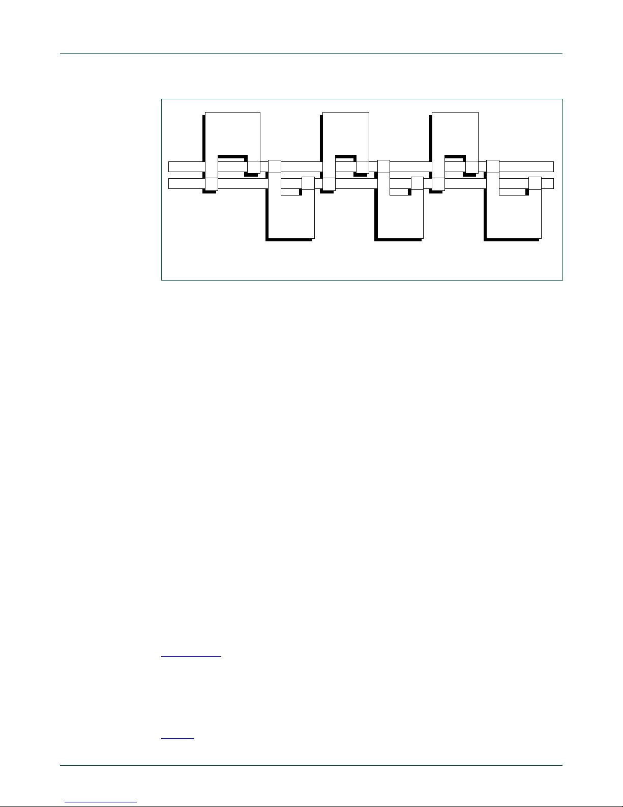
Two wires, serial data (SDA) and serial clock (SCL), carry information between the
devices connected to the bus. Each device is recognized by a unique address (whether
it is a microcontroller, LCD driver, memory or keyboard interface) and can operate as
either a transmitter or receiver, depending on the function of the device. An LCD driver
may be only a receiver , whereas a memory can b oth receive and transmit data. In ad dition
to transmitters and receivers, devices can also be considered as masters or slaves when
performing data transfers (see Table 1
). A master is the device which initiates a data
transfer on the bus and generates the clock signals to permit that transfer. At that time,
any device addressed is considered a slave.
The I2C-bus is a multi-master bus. This means that more than one device capable of
controlling the bus can be connected to it. As masters are usually microcontrollers, let us
consider the case of a data transfer between two microcontrollers connected to the
I
2
C-bus (see Figure 2).
T able 1. Definition of I2C-bus terminology
Term Description
Transmitter the device which sends data to the bus
Receiver the device which receives data from the bus
Master the device which initiates a transfer, generates clock signals and
terminates a transfer
Slave the device addressed by a master
Multi-master more than one master can attempt to control the bus at the same time
without corrupting the message
Arbitration procedure to ensure that, if more than one master simultaneously tries to
control the bus, only one is allowed to do so and the winning message is
not corrupted
Synchronization procedure to synchronize the clock signals of two or more devices
Page 7
UM10204 All information provided in this document is subject to legal disclaimers. © NXP B.V. 2012. All rights reserved.
User manual Rev. 5 — 9 October 2012 7 of 64
NXP Semiconductors
UM10204
I2C-bus specification and user manual
This example highlights the master-slave and receiver-transmitter relationships found on
the I
2
C-bus. Note that these relationships are not permanent, but only depend on the
direction of data transfer at that time. The transfer of data would proceed as follows:
1. Suppose microcontroller A wants to send information to microcontroller B:
– microcontroller A (master), addresses microcontroller B (slave)
– microcontroller A (master-transmitter), sends data to microcontroller B
(slave-receiver)
– microcontroller A terminates the transfer.
2. If microcontroller A wants to receive information from microcontroller B:
– microcontroller A (master) addresses microcontroller B (slave)
– microcontroller A (master-receiver) receives data from microcontroller B
(slave-transmitter)
– microcontroller A terminates the transfer.
Even in this case, the master (microcontroller A) generates the timing and terminates the
transfer.
The possibility of connecting more than one microcontroller to the I
2
C-bus means that
more than one master could try to initiate a data transfer at the same time. To avoid the
chaos that might ensue from such an event, an arbitration pro cedure has been developed.
This procedure relies on the wired-AND connection of all I
2
C interfaces to the I2C-bus.
If two or more masters try to put information onto the bus, the first to pr oduce a ‘one’ when
the other produces a ‘zero’ loses the arbitration. The clock sign als dur ing ar bitr ation are a
synchronized combination of the clocks generated by the masters using the wired-AND
connection to the SCL line (for more detailed information concerning arbitration see
Section 3.1.8
).
Generation of clock signals on the I
2
C-bus is always the responsibility of master devices;
each master generates its own clock signals when transferrin g dat a on the bus. Bus clock
signals from a master can only be altered when they are stretched by a slow slave device
holding down the clock line or by another master when arbitration occurs.
Table 2
summarizes the use of mandatory and optional portions of the I2C-bus
specification and which system configurations use them.
Fig 2. Example of an I2C-bus configuration using two microcontrol le rs
mbc645
SDA
SCL
MICRO CONTROLLER
A
STATIC
RAM OR
EEPROM
LCD
DRIVER
GATE
ARRAY
ADC
MICRO CONTROLLER
B
Page 8
UM10204 All information provided in this document is subject to legal disclaimers. © NXP B.V. 2012. All rights reserved.
User manual Rev. 5 — 9 October 2012 8 of 64
NXP Semiconductors
UM10204
I2C-bus specification and user manual
[1] Also refers to a master acting as a slave.
[2] Clock stretching is a feature of some slaves. If no slaves in a system can stretch the clock (hold SCL LOW),
the master need not be designed to handle this procedure.
[3] ‘Bit banging’ (software emulation) multi-master systems should consider a START byte. See
Section 3.1.15
.
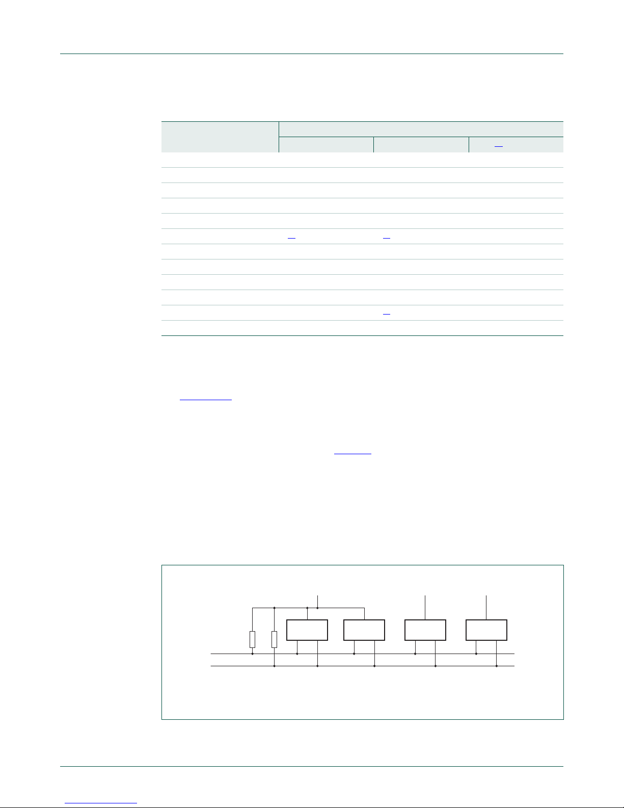
3.1.1 SDA and SCL signals
Both SDA and SCL are bidirectional lines, connected to a positive supply voltage via a
current-source or pull-up resistor (see Figure 3
). When the bus is free, both lines are
HIGH. The output stages of devices connected to the bus must have an open-drain or
open-collector to perform the wired-AND function. Data on th e I
2
C-bus can be transferred
at rates of up to 100 kbit/s in the Standard-mode, up to 400 kbit/s in the Fast-mode, up to
1 Mbit/s in Fast-mode Plus, or up to 3.4 Mbit/s in the High-speed mode. The bus
capacitance limits the number of interfaces connected to the bus.
For a single master application, the master’s SCL output can be a push-pull driver design
if there are no devices on the bus which would stretch the clock.
T able 2. Applicability of I2C-bus protocol features
M = mandatory; O = optional; n/a = not applicable.
Feature Configuration
Single master Multi-master Slave
[1]
START condition M M M
STOP condition M M M
Acknowledge M M M
Synchronization n/a M n/a
Arbitration n/a M n/a
Clock stretching O
[2]
O
[2]
O
7-bit slave address M M M
10-bit slave address O O O
General Call address O O O
Software Reset O O O
START byte n/a O
[3]
n/a
Device ID n/a n/a O
V
DD2
, V
DD3
are device-dependent (for example, 12 V).
Fig 3. Devices with various supply voltages sharing the same bus
CMOS CMOS NMOS BIPOLAR
002aac860
V
DD1
=
5 V ± 10 %
R
p
R
p
SDA
SCL
V
DD2
V
DD3
Page 9
UM10204 All information provided in this document is subject to legal disclaimers. © NXP B.V. 2012. All rights reserved.
User manual Rev. 5 — 9 October 2012 9 of 64
NXP Semiconductors
UM10204
I2C-bus specification and user manual
3.1.2 SDA and SCL logic levels
Due to the variety of different technology devices (CMOS, NMOS, bipolar) that can be
connected to the I
2
C-bus, the levels of the logical ‘0’ (LOW) and ‘1’ (HIGH) are not fixed
and depend on the associated level of V
DD
. Input reference levels are set as 30 % and
70 % of V
DD
; VIL is 0.3VDD and VIH is 0.7VDD. See Figure 38, timing diagram. Some
legacy device input levels were fixed at V
IL
= 1.5 V and VIH= 3.0 V, but all new devices
require this 30 %/70 % specification. See Section 6
for electrical specifications.
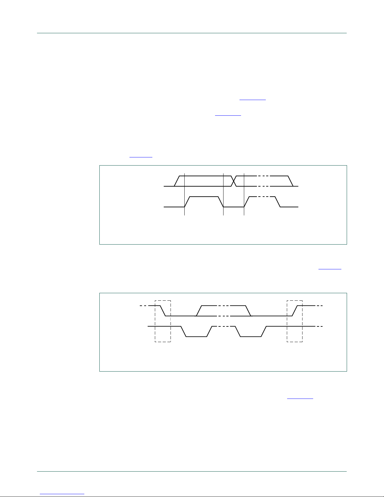
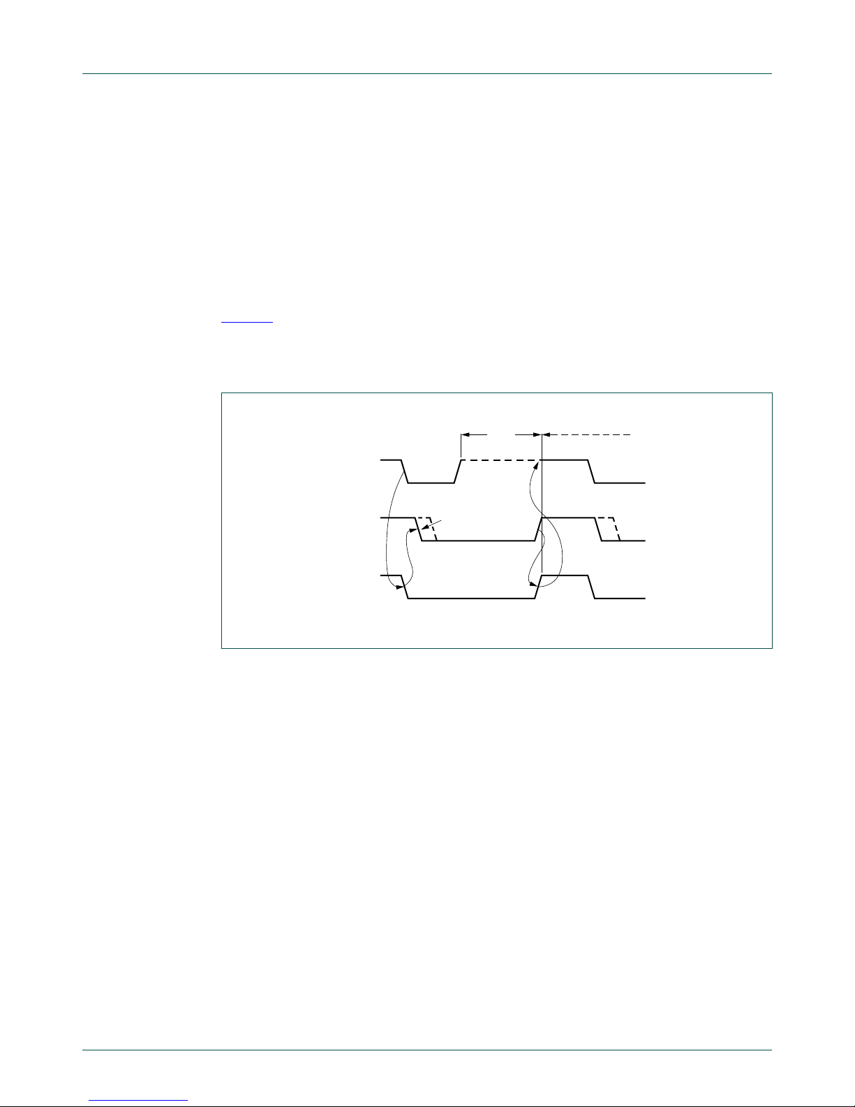
3.1.3 Data validity
The data on the SDA line must be stable during the HIGH period of the clock. The HIGH
or LOW state of the data line can only change when the clock signal on the SCL line is
LOW (see Figure 4
). One clock pulse is generated for each data bit transferred.
3.1.4 START and STOP conditions
All transactions begin with a START (S) and are terminated by a STOP (P) (see Figure 5).
A HIGH to LOW transition on the SDA line while SCL is HIGH defines a START condition.
A LOW to HIGH transition on the SDA line while SCL is HIGH defines a STOP condition.
START and STOP conditions ar e a lwa ys ge ne ra te d by the m aster. The bus is considered
to be busy after the START condition. The bus is considered to be free again a cert ain
time after the STOP condition. This bus free situation is specified in Section 6
.
The bus stays busy if a repeated START (Sr) is generated instead of a STOP condition. In
this respect, the ST ART (S) and repeated START (Sr) conditions are functionally identical.
For the remainder of this document, therefore, the S symbol is used as a generic ter m to
represent both the START and repeated START conditions, unless Sr is particularly
relevant.
Fig 4. Bit transfer on the I2C-bus
mba607
data line
stable;
data valid
change
of data
allowed
SDA
SCL
Fig 5. START and STOP conditions
mba608
SDA
SCL
P
STOP condition
S
START condition
Page 10
UM10204 All information provided in this document is subject to legal disclaimers. © NXP B.V. 2012. All rights reserved.
User manual Rev. 5 — 9 October 2012 10 of 64
NXP Semiconductors
UM10204
I2C-bus specification and user manual
Detection of START and STOP conditions by devices connected to the bus is easy if they
incorporate the necessary interfacing hardwar e. However, microcontroller s with no such
interface have to sample the SDA line at least twice per clock period to sense the
transition.
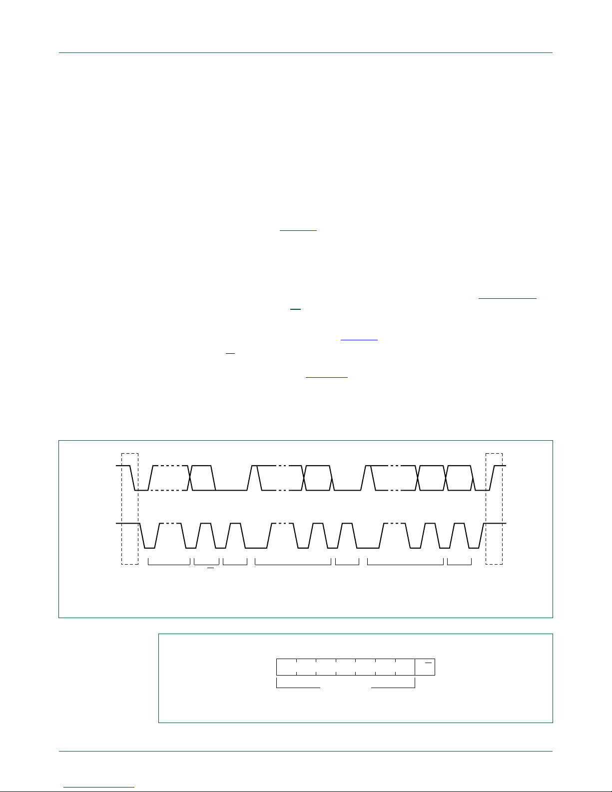
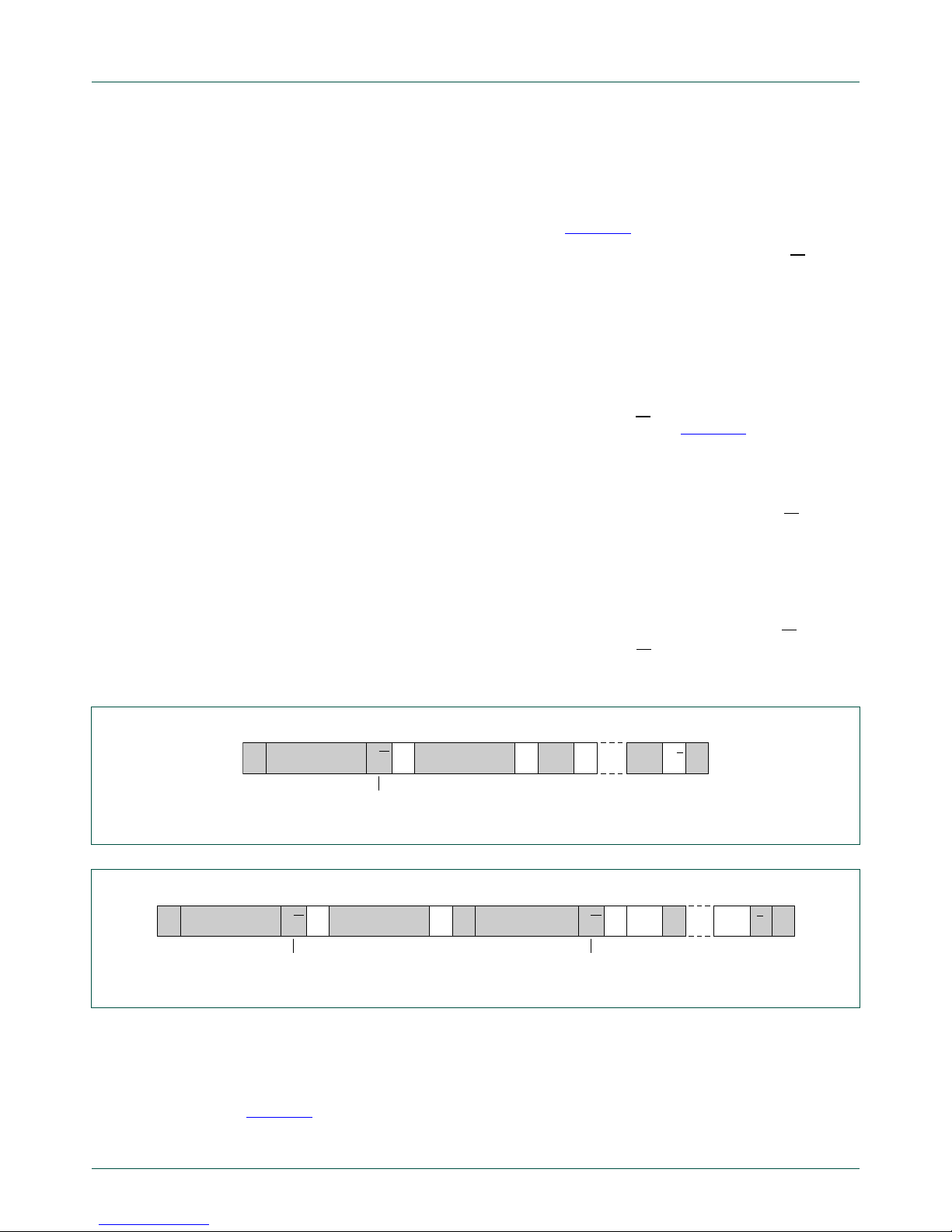
3.1.5 Byte format
Every byte put on the SDA line must be eight bits long. The number of bytes that can be
transmitted per transfer is unrestricted. Each byte must be followed by an Acknowledge
bit. Data is transferred with the Most Significant Bit (MSB) first (see Figure 6
). If a slave
cannot receive or transmit another complete byte of dat a until it has performed some other
function, for example servicing an internal interrupt, it can hold the clock line SCL LOW to
force the master into a wait state. Data tr ansfer then continue s when th e slave is ready for
another byte of data and releases clock line SCL.
3.1.6 Acknowledge (ACK) and Not Acknowledge (NACK)
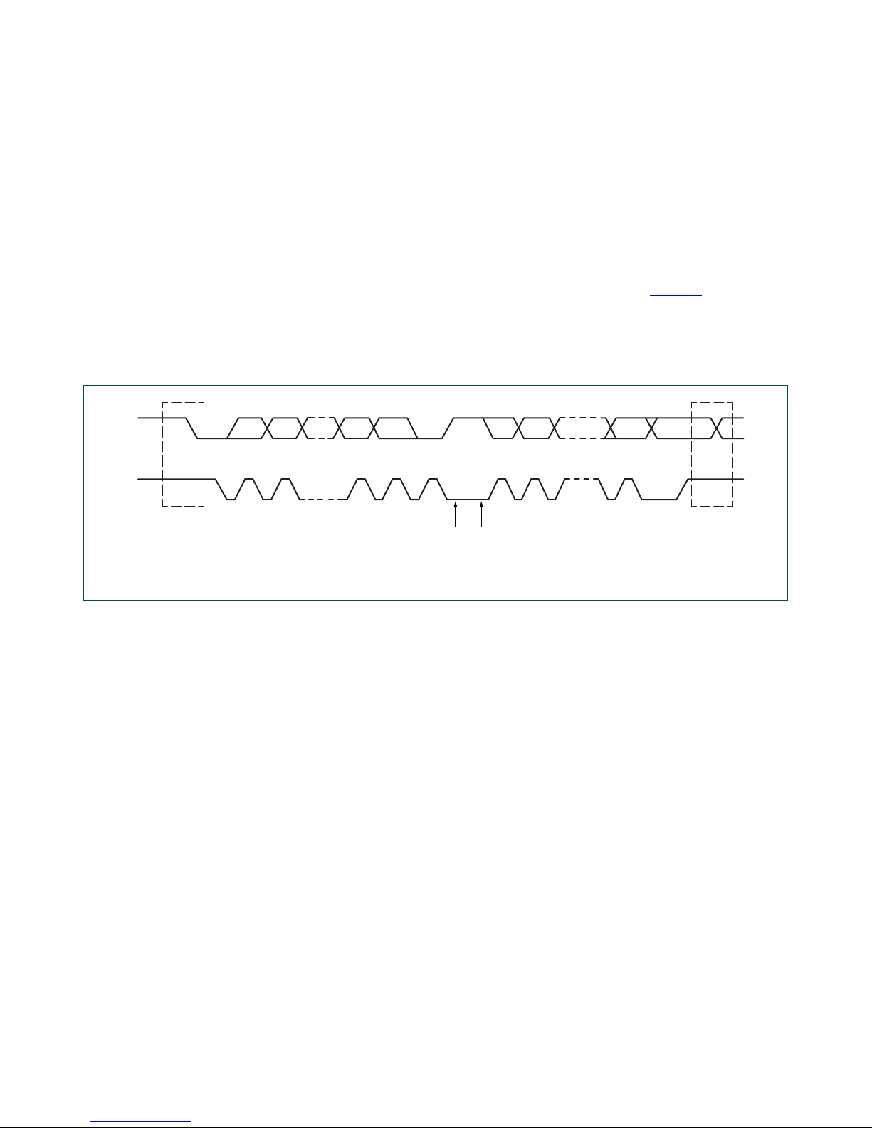
The acknowledge takes place after e very byte. The acknowledge bit allows the receiver to
signal the transmitter that the byte was successfully received and another byte may be
sent. The master generates all clock pulses, including the acknowledge ninth clock pulse.
The Acknowledge signal is defined as follows: the transmitter releases the SDA line
during the acknowledge clock pulse so the receiver can pull the SDA line LOW and it
remains stable LOW during the HIGH period of th is clock pulse (see Figure 4
). Set-up and
hold times (specified in Section 6
) must also be taken into account.
When SDA remains HIGH during this ninth clock pulse, this is defined as the Not
Acknowledge signal. The master can then generate either a STOP condition to abort the
transfer, or a repeated START condition to start a new transfer. There are five conditions
that lead to the generation of a NACK:
1. No receiver is present on the bus with the transmitted address so there is no device to
respond with an acknowledge.
2. The receiver is unable to receive or transmit because it is performing some real-time
function and is not ready to start communication with the master.
3. During the transfer, the receiver gets data or commands that it does not understand.
4. During the transfer, the receiver cannot receive any more data bytes.
5. A master-receiver must signal the end of the transfer to the slave transmitter.
Fig 6. Data transfer on the I2C-bus
S or Sr Sr or P
SDA
SCL
MSB
1 2 7 8 9 1 2 3 to 8 9
ACK ACK
002aac861
START or
repeated START
condition
STOP or
repeated START
condition
acknowledgement
signal from slave
byte complete,
interrupt within slave
clock line held LOW
while interrupts are serviced
P
Sr
acknowledgement
signal from receiver
Page 11
UM10204 All information provided in this document is subject to legal disclaimers. © NXP B.V. 2012. All rights reserved.
User manual Rev. 5 — 9 October 2012 11 of 64
NXP Semiconductors
UM10204
I2C-bus specification and user manual
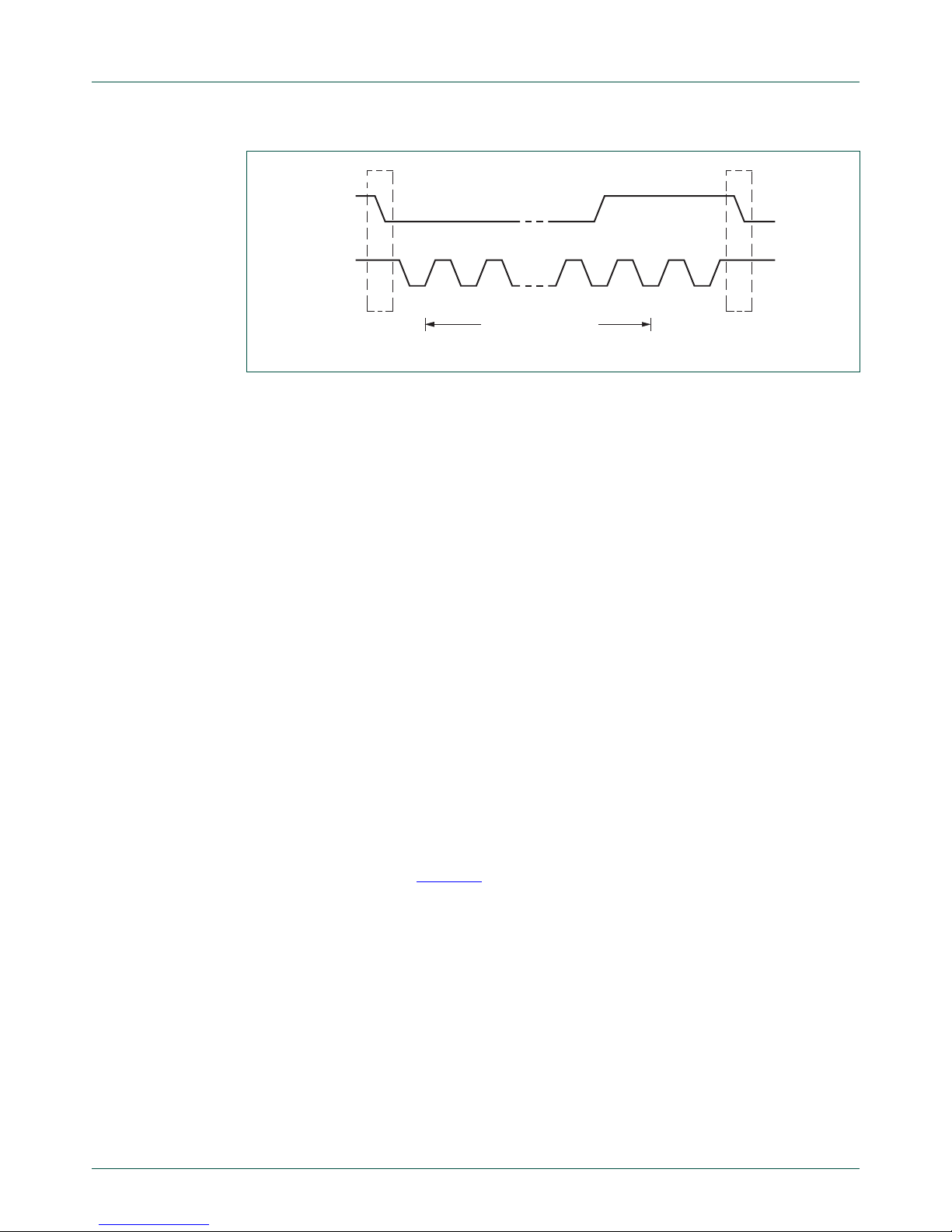
3.1.7 Clock synchronization
Two masters can begin transmitting on a free bus at the same time and there must be a
method for deciding which takes control of the bus and complete its transmission. This is
done by clock synchronization and arbitration. In single master systems, clock
synchronization and arbitration are not needed.
Clock synchronization is performed using the wired-AND connection of I
2
C interfaces to
the SCL line. This means that a HIGH to LOW transition on the SCL line causes the
masters concerned to start counting off their LOW period and, once a master clock has
gone LOW, it holds the SCL line in that state until the clock HIGH state is reached (see
Figure 7
). However, if another clock is still within its LOW period, the LOW to HIGH
transition of this clock may not change the sta te of the SCL line. Th e SCL line is therefore
held LOW by the master with the longest LOW period. Masters with shorter LOW periods
enter a HIGH wait-state during this time.
When all masters concerned have counted off their LOW period, the clock line is released
and goes HIGH. There is then no difference between the master clocks and the state of
the SCL line, and all the masters start counting their HIGH periods. The first master to
complete its HIGH period pulls the SCL line LOW again.
In this way , a synchronized SCL clock is gene rated with its LOW period determined by the
master with the longest clock LOW period, and its HIGH period determined by the one
with the shortest clock HIGH period.
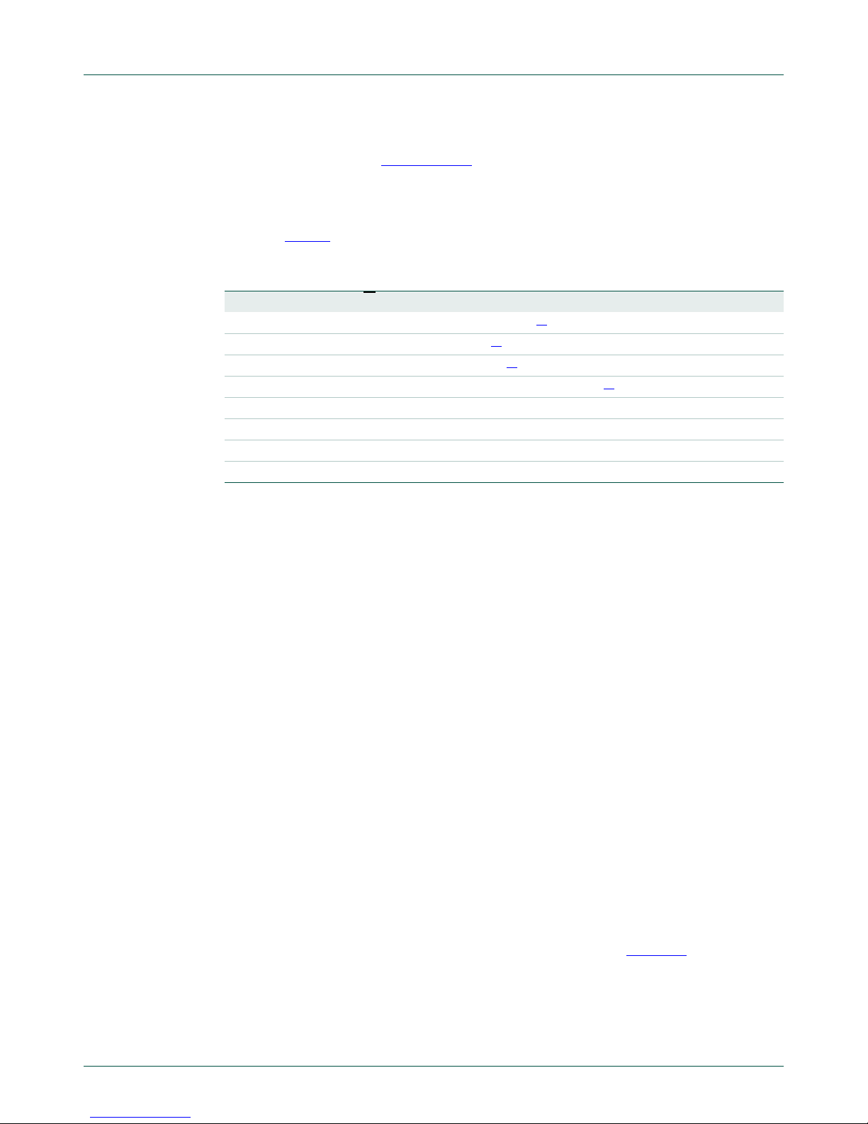
3.1.8 Arbitration
Arbitration, like synchronization, refe rs to a portio n of th e pr ot oco l req u ire d on ly if mo re
than one master is used in the system. Slaves are not involved in the arbitration
procedure. A master may start a transfer only if the bus is free. Two masters may
generate a START condition within the minimum hold time (t
HD;STA
) of the START
condition which results in a valid START condition on the bus. Arbitration is then required
to determine which master will complete its transmission.
Arbitration proceeds bit by bit. During every bit, while SCL is HIGH, each master checks to
see if the SDA level matches what it has sent. This process may take many bits. Two
masters can actually complete an entire transaction without error, as long as the
Fig 7. Clock synchronization during the arbitration procedure
CLK
1
CLK
2
SCL
counter
reset
wait
state
start counting
HIGH period
mbc632
Page 12

UM10204 All information provided in this document is subject to legal disclaimers. © NXP B.V. 2012. All rights reserved.
User manual Rev. 5 — 9 October 2012 12 of 64
NXP Semiconductors
UM10204
I2C-bus specification and user manual
transmissions are identical. The first time a master tries to send a HIGH, but detects that
the SDA level is LOW, the master knows that it has lost the arbitration and turns off its
SDA output driver. The other master goes on to complete its transaction.
No information is lost during the arbitration process. A master that loses the arbitration
can generate clock pulses until the end of the byte in which it loses the arbitration and
must restart its transaction when the bus is free.
If a master also incorporates a slave function and it loses arbitration during the addressing
stage, it is possible that the winning master is trying to address it. The losing maste r must
therefore switch over immediately to its slave mode.
Figure 8
shows the arbitration procedure for two masters. More may be involved
depending on how many masters are connected to the bus. The moment there is a
difference between the internal data level of the master generating DATA1 and the actual
level on the SDA line, the DATA1 output is switched off. This does not affect the data
transfer initiated by the winning master.
Since control of the I2C-bus is decided solely on the address and data sent by competing
masters, there is no central master, nor any order of priority on the bus.
There is an undefined condition if the arbitration procedure is still in progress at the
moment when one master sends a repeated START or a STOP condition while the other
master is still sending data. In other words, the following combinations result in an
undefined condition:
• Master 1 sends a repeated START condition and master 2 sends a data bit.
• Master 1 sends a STOP condition and master 2 sends a data bit.
• Master 1 sends a repeated START condition and master 2 sends a STOP condition.
Fig 8. Arbitration procedure of two masters
msc609
DATA
1
DATA
2
SDA
SCL
S
master 1 loses arbitration
DATA 1 SDA
Page 13
UM10204 All information provided in this document is subject to legal disclaimers. © NXP B.V. 2012. All rights reserved.
User manual Rev. 5 — 9 October 2012 13 of 64
NXP Semiconductors
UM10204
I2C-bus specification and user manual
3.1.9 Clock stretching
Clock stretching pauses a transaction by holding the SCL line LOW. The transaction
cannot continue until the line is released HIGH again. Clock stretching is optional and in
fact, most slave devices do not include an SCL driver so they are unable to stretch the
clock.
On the byte level, a device may be able to receive bytes of data at a fast rate, but needs
more time to store a received byte or prepare another byte to be transmitted. Slaves can
then hold the SCL line LOW after reception and acknowledgment of a byte to force the
master into a wait state until the slave is ready for the next byte transfer in a type of
handshake procedure (see Figure 7
).
On the bit level, a device such as a microcontroller with or without limited har dware for the
I
2
C-bus, can slow down the bus clock by extending each clock LOW period. The speed of
any master is adapted to the internal operating rate of this device.
In Hs-mode, this handshake feature can only be used on byte level (see Section 5.3.2
).
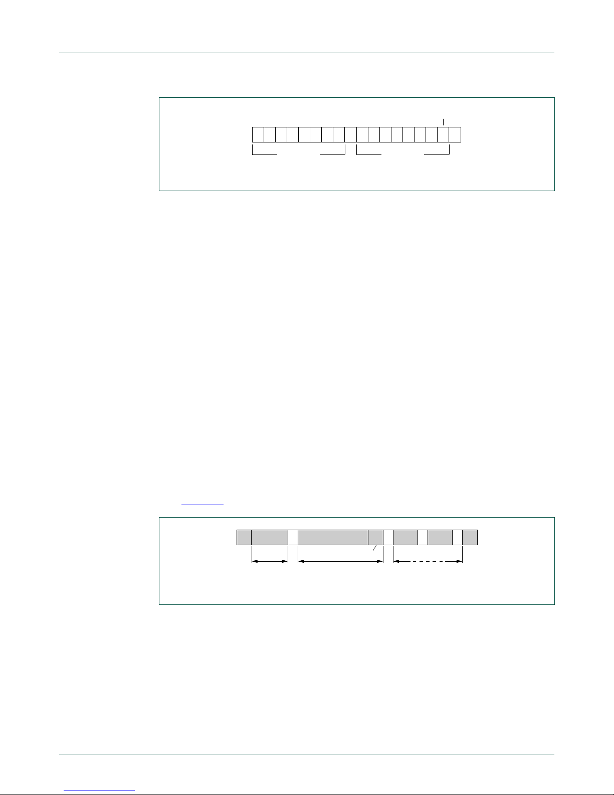
3.1.10 The slave address and R/W bit
Data transfers follow the format shown in Figure 9. After the START condition (S), a slave
address is sent. This address is seven bits long followed by an eighth bit which is a data
direction bit (R/W
) — a ‘zero’ indicates a transmission (WRITE), a ‘one’ indicates a
request for data (READ) (refer to Figure 10
). A data transfer is always terminated by a
STOP condition (P) generated by the master. However, if a master still wishes to
communicate on the bus, it can generate a repeated START condition (Sr) and address
another slave without first generating a STOP condition. Various combinations of
read/write formats are then possible within such a transfer.
Fig 9. A complete data transfer
S
1 - 7 8 9 1 - 7 8 9 1 - 7 8 9
P
STOP
condition
START
condition
DATA ACKDATA ACKADDRESS ACKR/W
SDA
SCL
mbc604
Fig 10. The first byte after the START procedure
mbc608
R/W
LSBMSB
slave address
Page 14

UM10204 All information provided in this document is subject to legal disclaimers. © NXP B.V. 2012. All rights reserved.
User manual Rev. 5 — 9 October 2012 14 of 64
NXP Semiconductors
UM10204
I2C-bus specification and user manual
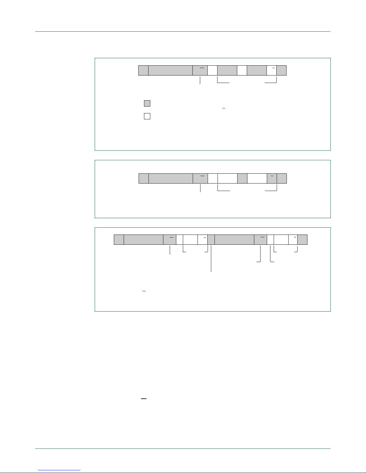
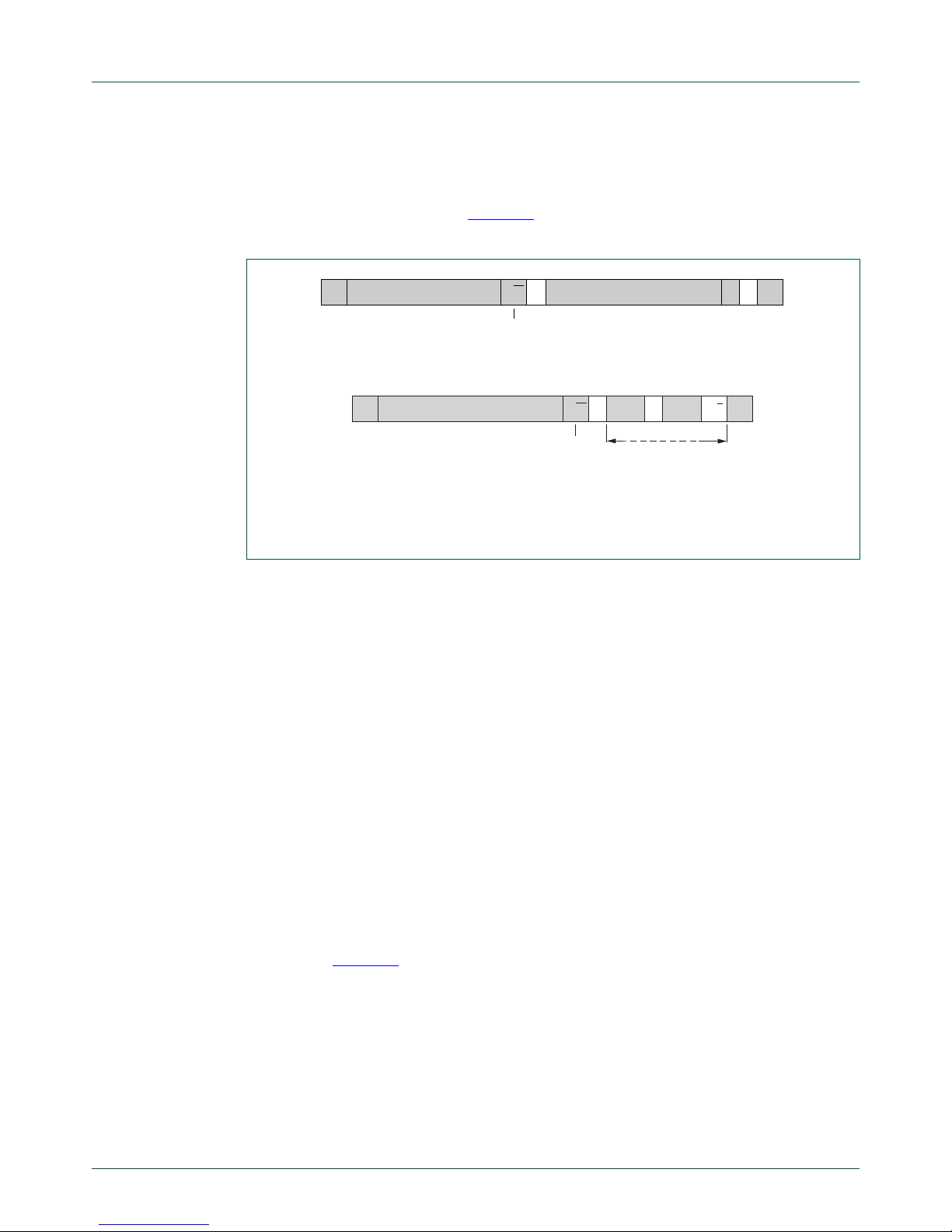
Possible data transfer formats are:
• Master-transmitter transmits to slave-receiver. The transfer direction is not changed
(see Figure 11
). The slave receiver acknowledges each byte.
• Master reads slave immediately after first byte (see Figure 12). At the moment of the
first acknowledge, the master-transmitter becomes a master-receiver and the
slave-receiver becomes a slave-transmitter. This first acknowledge is still generated
by the slave. The master generates subsequent acknowledges. The STOP condition
is generated by the master , which sends a not-acknowledge ( A
) just before the STOP
condition.
• Combined format (see Figure 13). During a change of direction within a transfer, the
START condition and the slave address are both repeated, but with the R/W
bit
reversed. If a master-receiver sends a repeated START condition, it sends a
not-acknowledge (A
) just before the repeated START condition.
Notes:
1. Combined formats can be used, for example, to control a serial memory. The internal
memory location must be written during the first data byte. After the START condition
and slave address is repeated, data can be transferred.
2. All decisions on auto-increment or decrement of previously accessed memory
locations, etc., are taken by the designer of the device.
3. Each byte is followed by an acknowledgment bit as indicated by the A or A
blocks in
the sequence.
4. I
2
C-bus compatible devices must reset their bus logic on receipt of a START or
repeated START condition such that they all anticipate the sending of a slave
address, even if these START conditions are not positioned according to the proper
format.
5. A START condition immediately followed by a STOP condition (void message) is an
illegal format. Many devices however are designed to operate properly under this
condition.
6. Each device connected to the bus is addressable by a unique address. Normally a
simple master/slave relationship exists, but it is possible to have multiple identical
slaves that can receive and respond simultaneously, for example in a group
broadcast. This technique works best when using bus switching devices like the
PCA9546A where all four channels are on and identical devices are con figured a t the
same time, understanding that it is impossible to determine that each slave
acknowledges, and then turn on one channel at a time to read back each individual
device’s configuration to confirm the programming. Refer to individual component
data sheets.
Page 15
UM10204 All information provided in this document is subject to legal disclaimers. © NXP B.V. 2012. All rights reserved.
User manual Rev. 5 — 9 October 2012 15 of 64
NXP Semiconductors
UM10204
I2C-bus specification and user manual
3.1.11 10-bit addressing
10-bit addressing expands the number of possible addresses. Devices with 7-bit and
10-bit addresses can be connected to the same I
2
C-bus, and both 7-bit and 10-bit
addressing can be used in all bus speed modes. Currently, 10-bit addressing is not being
widely used.
The 10-bit slave address is formed from the first two bytes following a START condition
(S) or a repeated START condition (Sr).
The first seven bits of the first byte are the combination 11 11 0XX of which the last two bits
(XX) are the two Most-Significant Bits (MSB) of the 10-bit address; the eighth bit of the
first byte is the R/W
bit that determines the direction of the messag e.
Although there are eight possible combina tions of the reserved address bits 1111 XXX,
only the four combinations 1111 0XX are used for 10-bit addressing. The remaining four
combinations 1111 1XX are reserved for future I
2
C-bus enhancements.
Fig 11. A maste r-tran smitter addressing a slave receiver with a 7-bit address
(the transfer direction is not changed)
Fig 12. A master reads a slave immediately after the first byte
Fig 13. Combined format
mbc605
A/A
A
'0' (write)
data transferred
(n bytes + acknowledge)
A = acknowledge (SDA LOW)
A = not acknowledge (SDA HIGH)
S = START condition
P = STOP condition
R/W
from master to slave
from slave to master
DATADATAASLAVE ADDRESSS P
mbc606
A
(read)
data transferred
(n bytes + acknowledge)
R/W A1PDATADATASLAVE ADDRESSSA
mbc607
DATAAR/W
read or write
A/A
DATAAR/W
(n bytes
+ ack.)
*
direction of transfer
may change at this
point.
read or write
(n bytes
+ ack.)
*
Sr = repeated START condition
A/A
*
not shaded because
transfer direction of
data and acknowledge bits
depends on R/W bits.
SLAVE ADDRESSSSrPSLAVE ADDRESS
Page 16
UM10204 All information provided in this document is subject to legal disclaimers. © NXP B.V. 2012. All rights reserved.
User manual Rev. 5 — 9 October 2012 16 of 64
NXP Semiconductors
UM10204
I2C-bus specification and user manual
All combinations of read/write formats prev iously described for 7-bit addressing are
possible with 10-bit addressing. Two are detailed here:
• Master-transmitter transmits to slave-receiver with a 10-bit slave address.
The transfer direction is not changed (see Figure 14
). When a 10-bit address follows
a START condition, each slave compares the first seven bits of the first byte of the
slave address (1111 0XX) with its own address and tests if the eighth bit (R/W
direction bit) is 0. It is possible that more than one device finds a match and generate
an acknowledge (A1). All slaves that found a match compare the eight bits of the
second byte of the slave address (XXXX XXXX) with their own addresse s, but only
one slave finds a match and generates an acknowledge (A2). The matching slave
remains addressed by the master until it receive s a ST OP co nditio n (P) o r a repe ated
START condition (Sr) followed by a different slave address.
• Master-receiver reads slave-transmitter with a 10-bit slave address.
The transfer direction is changed after the second R/W
bit (Figure 15). Up to and
including acknowledge bit A2, the procedure is the same as that described for a
master-transmitter addressing a slave-receiver. After the repeated START condition
(Sr), a matching slave remembers that it was addressed before. This slave then
checks if the first seven bits of the first byte of the slave address following Sr are the
same as they were after the START condition (S), and tests if the eighth (R/W
) bit is 1.
If there is a match, the slave considers that it has been addressed as a transmitter
and generates acknowledge A3. The slave-transmitter remains addressed until it
receives a STOP condition (P) or until it receives another repeated START condition
(Sr) followed by a different slave address. After a repeated START condition (Sr), all
the other slave devices will also compare the first seven bits of the first byte of the
slave address (1111 0XX) with their own addresses and test the eighth (R/W
) bit.
However, none of them will be addressed because R/W
= 1 (for 10-bit devices), or the
1111 0XX slave address (for 7-bit devices) does not match.
Slave devices with 10-bit addressing react to a ‘general call’ in the same way as slave
devices with 7-bit addressing. Hardware masters can transmit their 10-bit address after a
‘general call’. In this case, the ‘general call’ address byte is followed by two successive
bytes containing the 10-bit address of the master-transmitter. The format is as shown in
Figure 15
where the first DATA byte contains the eight least-significant bits of the master
address.
Fig 14. A master-transmitter addresses a slave-receiver with a 10-bit address
mbc613
R/W
A1
(write)
A2
A
A/A
1 1 1 1 0 X X 0
SLAVE ADDRESS
1st 7 BITS
S DATA PDATA
SLAVE ADDRESS
2nd BYTE
Fig 15. A master-receiver addresses a slave-transmitter with a 10-bit address
mbc614
R/W A1
(write)
A3 DATA DATAA2 R/W
(read)
1 1 1 1 0 X X 0 1 1 1 1 0 X X 1
A
APSr
SLAVE ADDRESS
1st 7 BITS
SLAVE ADDRESS
2nd BYTE
SLAVE ADDRESS
1st 7 BITS
S
Page 17
UM10204 All information provided in this document is subject to legal disclaimers. © NXP B.V. 2012. All rights reserved.
User manual Rev. 5 — 9 October 2012 17 of 64
NXP Semiconductors
UM10204
I2C-bus specification and user manual
The START byte 0000 0001 (01h) can precede the 10-bit addressing in the same way as
for 7-bit addressing (see Section 3.1.15
).
3.1.12 Reserved addresses
Two groups of eight addresses (0000 XXX and 1111 XXX) are reserved for the purposes
shown in Table 3
.
[1] The general call address is used for several functions including software reset.
[2] No device is allowed to acknowledge at the reception of the START byte.
[3] The CBUS address has been reserved to enable the inter-mixing of CBUS compatible and I
2
C-bus
compatible devices in the same system. I
2
C-bus compatible devices are not allowed to respond on
reception of this address.
[4] The address reserved for a different bus format is included to enable I
2
C and other protocols to be mixed.
Only I
2
C-bus compatible devices that can work with such formats and protocols are allowed to respond to
this address.
Assignment of addresses within a local system is up to the system architect who must
take into account the devices being used on the bus and any future interaction with other
conventional I
2
C-buses. For example, a device with seven user-assignable address pins
allows all 128 addresses to be assigned. If it is known that the reserved address is never
going to be used for its intended purpose, a reserved address can be used for a slave
address.
3.1.13 General call address
The general call address is for addressing every device connected to the I2C-bus at the
same time. However, if a device does not need any of the data supplied within the general
call structure, it can ignore this address by not issuing an acknowledgment. If a device
does require data from a general call address, it acknowledges this address and behave
as a slave-receiver. The master does not actually know how many devices acknowledged
if one or more devices respond. The second and following bytes are acknowledged by
every slave-receiver capable of handling this data. A slave who cannot process one of
these bytes must ignore it by not-acknowledging. Again, if one or more slaves
acknowledge, the not-acknowledge will not be seen by the master. The meaning of the
general call address is always specified in the second byte (see Figure 16
).
Table 3. Reserved addresses
X = don’t care; 1 = HIGH; 0 = LOW.
Slave address R/W bit Description
0000 000 0 general call address
[1]
0000 000 1 START byte
[2]
0000 001 X CBUS address
[3]
0000 010 X reserved for different bus format
[4]
0000 011 X reserved for future purposes
0000 1XX X Hs-mode master code
1111 1XX 1 device ID
1111 0XX X 10-bit slave addressing
Page 18
UM10204 All information provided in this document is subject to legal disclaimers. © NXP B.V. 2012. All rights reserved.
User manual Rev. 5 — 9 October 2012 18 of 64
NXP Semiconductors
UM10204
I2C-bus specification and user manual
There are two cases to consider:
• When the least significant bit B is a ‘zero’.
• When the least significant bit B is a ‘one’.
When bit B is a ‘zero’, the second byte has the following definition:
• 0000 0110 (06h): Reset and write programmable part of slave address by
hardware. On receiving this 2-byte sequence, all devices designed to respond to the
general call address reset and take in the programmable part of their address.
Precautions must be taken to ensure that a device is not pulling down the SDA or SCL
line after applying the supply voltage, since these low levels would block the bus.
• 0000 0100 (04h): Write programmable part of slave address by hardware.
Behaves as above, but the device does not reset.
• 0000 0000 (00h): This code is not allowed to be used as the second byte.
Sequences of programming procedur e are pu blished in the appropriate device data
sheets. The remaining codes have not been fixed and devices must ignore them.
When bit B is a ‘one’, the 2-byte sequence is a ‘hardware general call’. This means that
the sequence is transmitted by a hardware master device, such as a keyboard scanner,
which can be programmed to transmit a desired slave address. Since a hardware master
does not know in advance to which device the message has to be transferred, it can only
generate this hardware general call and its own addre ss — ide ntifying itself to the system
(see Figure 17
).
The seven bits remaining in the second byte contain the address of the hardware ma ste r.
This address is recognized by an intelligent device (for example, a microcontroller)
connected to the bus which then accepts the information fr om the hardware master. If the
hardware master can also act as a slave, the slave address is identical to the master
address.
Fig 16. General call address format
Fig 17. Data transfer from a hardware master-transmitter
mbc623
LSB
second byte
0 0 0 0 0 0 0 0 A X X X X X X X BA
first byte
(general call address)
mbc624
general
call address
(B)
A A
second
byte
A A
(n bytes + ack.)
S 00000000 MASTER ADDRESS 1 PDATA DATA
Page 19
UM10204 All information provided in this document is subject to legal disclaimers. © NXP B.V. 2012. All rights reserved.
User manual Rev. 5 — 9 October 2012 19 of 64
NXP Semiconductors
UM10204
I2C-bus specification and user manual
In some systems, an alternative could be that the hardware master transmitter is set in the
slave-receiver mode after the system reset. In this way, a system configuring master can
tell the hardware master-transmitter (which is now in slave-receiver mode) to which
address data must be sent (see Figure 18
). After this programming procedure, the
hardware master remains in the master-transmitter mode.
3.1.14 Software reset
Following a General Call, (0000 0000), sending 0000 0110 (06h) as the second byte
causes a software reset. This feature is optional and not all devices respond to this
command. On receiving this 2-byte sequence, all devices designed to respond to the
general call address reset and take in the programmable part of their address.
Precautions must be taken to ensure that a device is not pulling down the SDA or SCL line
after applying the supply voltage, since these low levels would block the bus.
3.1.15 START byte
Microcontrollers can be connected to the I2C-bus in two ways. A microcontroller with an
on-chip hardware I
2
C-bus interface can be programmed to be only interrupted by r equests
from the bus. When the device does not have such an interface, it must constantly monitor
the bus via software. Obviously, the more times the microcontroller monitors, or polls the
bus, the less time it can spend carrying out its intended function.
There is therefore a speed dif ference between fast hardware devices and a relatively slow
microcontroller which relies on software polling.
In this case, data transfer can be preceded by a start procedure wh ich is much longer than
normal (see Figure 19
). The start procedure consists of:
• A START condition (S)
• A START byte (0000 0001)
• An acknowledge clock pulse (ACK)
• A repeated START condition (Sr).
a. Configuring master sends dump address to hardware master
b. Hardware master dumps data to selected slave
Fig 18. Data transfer by a hardware-transmitter capable of dumping data directly to slave
devices
002aac885
write
A
AR/WS PSLAVE ADDR. H/W MASTER DUMP ADDR. FOR H/W MASTER X
002aac886
R/W
write
A
A
(n bytes + ack.)
A/A
S PDUMP ADDR. FROM H/W MASTER DATA DATA
Page 20
UM10204 All information provided in this document is subject to legal disclaimers. © NXP B.V. 2012. All rights reserved.
User manual Rev. 5 — 9 October 2012 20 of 64
NXP Semiconductors
UM10204
I2C-bus specification and user manual
After the ST AR T condition S has been transmitted by a master which requires bus access,
the ST AR T byte (0 000 0001) is transmitted. Another microcontroller can therefore sample
the SDA line at a low sampling rate until one of the seven zeros in the START byte is
detected. After detection of this LOW level on the SDA line, the microcontroller can switch
to a higher sampling rate to find the repeated START condition Sr which is then used for
synchronization.
A hardware receiver resets upon receipt of the repeated START condition Sr and
therefore ignores the START byte.
An acknowledge-related clock pulse is generated after the START byte. This is present
only to conform with the byte handling format used on the bus. No device is allowed to
acknowledge the START byte.
3.1.16 Bus clear
In the unlikely event where the clock (SCL) is stuck LOW, the preferential procedure is to
reset the bus using the HW reset signal if your I
2
C devices have HW reset inputs. If the
I
2
C devices do not have HW reset inputs, cycle power to the devices to activate the
mandatory internal Power-On Reset (POR) circuit.
If the data line (SDA) is stuck LOW , the master should send nine cloc k pulses. The device
that held the bus LOW should release it sometime within those nine clocks. If not, then
use the HW reset or cycle power to clear the bus.
3.1.17 Device ID
The Device ID field (see Figure 20) is an optional 3-byte read-only (24 bits) word giving
the following information:
• Twelve bit s with the manufacturer na me, unique per m anu factu rer ( for exam ple, NXP)
• Nine bits with the part identification, assigned by manufacturer (for example,
PCA9698)
• Three bits with the die revision, assigned by manufacturer (for example, RevX)
Fig 19. START byte procedure
002aac997
S
9821
Sr
7
NACK
dummy
acknowledge
(HIGH)
START byte 0000 0001
SDA
SCL
Page 21

UM10204 All information provided in this document is subject to legal disclaimers. © NXP B.V. 2012. All rights reserved.
User manual Rev. 5 — 9 October 2012 21 of 64
NXP Semiconductors
UM10204
I2C-bus specification and user manual
The Device ID is read-only, hard-wired in the device and can be accessed as follows:
1. START condition
2. The master sends the Reserved Device ID I
2
C-bus address followed by the R/W bit
set to ‘0’ (write): ‘11111000’.
3. The master sends the I
2
C-bus slave address of the slave device it must identify. The
LSB is a ‘Don’t care’ value. Only one device must acknowledge this byte (the one that
has the I
2
C-bus slave address).
4. The master sends a Re-START condition.
Remark: A STOP condition followed by a START condition resets the slave state
machine and the Device ID Read cannot be performed. Also, a STOP condition or a
Re-START condition followed by an access to another slave device resets the slave
state machine and the Device ID Read cannot be performed.
5. The master sends the Reserved Device ID I
2
C-bus address followed by the R/W bit
set to ‘1’ (read): ‘11111001’.
6. The Device ID Read can be done, starting with the 12 manufacturer bits (first byte +
four MSBs of the second byte), followed by the nine part identification bits (four LSBs
of the second byte + five MSBs of the third byte), and then the three die revision bits
(three LSBs of the third byte).
7. The master ends the reading sequence by NACKing the last byte, thus resetting the
slave device state machine and allowing the master to send the STOP condition.
Remark: The reading of the Device ID can be stopped anytime by sending a NACK.
If the master continues to ACK the bytes after the third byte, the slave rolls back to the first
byte and keeps sending the Device ID sequence until a NACK has been detected.
Fig 20. Device ID field
0
002aab942
0 0
00 0 0 0 0 0 0
00 0 0 0 0 0 0
revision
0
0 0 0 0
part identification
manufacturer
Page 22

UM10204 All information provided in this document is subject to legal disclaimers. © NXP B.V. 2012. All rights reserved.
User manual Rev. 5 — 9 October 2012 22 of 64
NXP Semiconductors
UM10204
I2C-bus specification and user manual
Designers of new I2C devices who want to implement the device ID feature should contact
NXP at i2c.support@nxp.com to have a unique manufacturer ID assigned.
Table 4. Assigned manufacturer IDs
Manufacturer bits Company
11 10 9 8 7 6 5 4 3 2 1 0
000000000000NXP Semiconductors
000000000001NXP Semiconductors (reserved)
000000000010NXP Semiconductors (reserved)
000000000011NXP Semiconductors (reserved)
000000000100Ramtron International
000000000101Analog Devices
000000000110STMicroelectronics
000000000111ON Semiconductor
000000001000Sprintek Corporation
000000001001ESPROS Photonics AG
000000001010Fujitsu Semiconductor
000000001011Flir
000000001100O
2
Micro
000000001101Atmel
Page 23

UM10204 All information provided in this document is subject to legal disclaimers. © NXP B.V. 2012. All rights reserved.
User manual Rev. 5 — 9 October 2012 23 of 64
NXP Semiconductors
UM10204
I2C-bus specification and user manual
3.2 Ultra Fast-mode I2C-bus protocol
The UFm I2C-bus is a 2-wire push-pull serial bus that operates from DC to 5 MHz
transmitting data in one direction. It is most useful for speeds greater than 1 MHz to drive
LED controllers and other devices that do not need feedback. The UFm I
2
C-bus protocol
is based on the standard I
2
C-bus protocol that consists of a START, slave address,
command bit, ninth clock, and a STOP bit. The command bit is a ‘write’ only, and the data
bit on the ninth clock is driven HIGH, ignoring the ACK cycle due to the unidirectional
nature of the bus. The 2-wire push-pull driver consists of a UFm serial clock (USCL) and
serial data (USDA).
Slave devices contain a unique address (whether it is a microcontroller, LCD driver, LED
controller, GPO) and operate only as receivers. An LED driver may be only a receiver and
can be supported by UFm, whereas a memory can both receive and transmit data and is
not supported by UFm.
Since UFm I
2
C-bus uses push-pull drivers, it does not have the multi-master capability of
the wired-AND open-drain Sm, Fm, and Fm+ I
2
C-buses. In UFm, a master is the only
device that initiates a data transfer on the bus and generates the clock signals to permit
that transfer. All other devices addressed are considered slaves.
Let us consider the case of a data transfer between a master and multiple slaves
connected to the UFm I
2
C-bus (see Figure 21).
T able 5. Definition of UFm I2C-bus terminology
Term Description
Transmitter the devi ce that send s data to the bus
Receiver the device that receives data from the bus
Master the device that initiates a transfer, generates clock signals and
terminates a transfer
Slave the device addressed by a master
Fig 21. E xample of UFm I
2
C-bus configuration
002aag654
USDA
USCL
Master ASIC LED
controller 3
LCD
DRIVER
LED
controller 1
LED
controller 2 GPO
Page 24

UM10204 All information provided in this document is subject to legal disclaimers. © NXP B.V. 2012. All rights reserved.
User manual Rev. 5 — 9 October 2012 24 of 64
NXP Semiconductors
UM10204
I2C-bus specification and user manual
This highlights the master/transmitter-slave/receiver relationship found on the UFm
I
2
C-bus. Note that these relationships are permane nt, as data transfer is only permitted in
one direction. The transfer of data would proceed as follows:
Suppose that the master ASIC wants to send information to the LED controller 2:
• ASIC A (master-transmitter), addresses LED controller 2 (slave-receiver) by sending
the address on the USDA and generating the clock on USCL.
• ASIC A (master-transmitter), sends data to LED controller 2 (slave-receiver) on the
USDA and generates the clock on USCL.
• ASIC A terminates the transfer.
The possibility of connecting more than one UFm master to the UFm I
2
C-bus is not
allowed due to bus contention on the push-pull output s. If an additio nal master is requ ired
in the system, it must be fully isolated from the other master (that is, with a true ‘one hot’
MUX) as only one master is allowed on the bus at a time.
Generation of clock signals on the UFm I
2
C-bus is always the responsibility of the master
device, that is, the master generates the clock signals when transferring data on the bus.
Bus clock signals from a master cannot be altered by a slave device with clock stretching
and the process of arbitration and clock synchronization does not exist within the UFm
I
2
C-bus.
Table 6
summarizes the use of mandatory and optional portions of the UFm I2C-bus
specification.
T able 6. Applicability of I2C-bus features to UFm
M = mandatory; O = optional; n/p = not possible
Feature Configuration
Single master
START condition M
STOP condition M
Acknowledge n/p
Synchronization n/p
Arbitration n/p
Clock stretching n/p
7-bit slave address M
10-bit slave address O
General Call address O
Software Reset O
START byte O
Device ID n/p
Page 25

UM10204 All information provided in this document is subject to legal disclaimers. © NXP B.V. 2012. All rights reserved.
User manual Rev. 5 — 9 October 2012 25 of 64
NXP Semiconductors
UM10204
I2C-bus specification and user manual
3.2.1 USDA and USCL signals
Both USDA and USCL are unidirectional lines, with push-pull outputs. When the bus is
free, both lines are pulled HIGH by the upper transistor of the output stage. Data on the
I
2
C-bus can be transferred at rates of up to 5000 kbit/s in the Ultra Fast-mode. The
number of interfaces connected to the bus is limited by the bus loading, reflections from
cable ends, connectors, and stubs.
3.2.2 USDA and USCL logic levels
Due to the variety of different technology devices (CMOS, NMOS, bipolar) that can be
connected to the I
2
C-bus, the levels of the logical ‘0’ (LOW) and ‘1’ (HIGH) are not fixed
and depend on the associated level of V
DD
. Input reference levels are set as 30 % and
70 % of V
DD
; VIL is 0.3VDD and VIH is 0.7VDD. See Figure 40, timing diagram. See
Section 6
for electrical specifications.
3.2.3 Data validity
The data on the USDA line must be stable during the HIGH period of the clock. The HIGH
or LOW state of the data line can only change when the clock signal on the USCL line is
LOW (see Figure 23
). One clock pulse is generated for each data bit transferred.
3.2.4 START and STOP conditions
Both data and clock lines remain HIGH when the bus is not busy. All transactions begin
with a START (S) and can be terminated by a STOP (P) (see Figure 24
). A HIGH to LOW
transition on the USDA line while USCL is HIGH defines a START condition. A LOW to
HIGH transition on the USDA line while USCL is HIGH defines a STOP condition.
Fig 22. Simplified schematic of USCL, USDA outputs
002aag655
V
DD(IO)
V
SS
USCL or
USDA pin
Fig 23. Bit transfer on the UFm I2C-bus
002aaf113
data line
stable;
data valid
change
of data
allowed
USDA
USCL
Page 26

UM10204 All information provided in this document is subject to legal disclaimers. © NXP B.V. 2012. All rights reserved.
User manual Rev. 5 — 9 October 2012 26 of 64
NXP Semiconductors
UM10204
I2C-bus specification and user manual
START and STOP conditions ar e a lwa ys ge ne ra te d by the m aster. The bus is considered
to be busy after the START condition. The bus is considered to be free again a cert ain
time after the STOP condition. This bus free situation is specified in Section 6
. The bus
stays busy if a repeated START (Sr) is generated instead of a STOP condition. In this
respect, the ST AR T (S) and repeated START (Sr) conditions are functionally identical. For
the remainder of this document, therefore, the S symbol is used as a generic term to
represent both the START and repeated START conditions, unless Sr is particularly
relevant.
Detection of START and STOP conditions by devices connected to the bus is easy if they
incorporate the necessary interfacing hardwar e. However, microcontroller s with no such
interface have to sample the USDA line at least twice per clock period to sense the
transition.
3.2.5 Byte format
Every byte put on the USDA line must be eight bits long. The number of bytes that can be
transmitted per transfer is unrestricted. The master drives the USDA HIGH after each byte
during the Acknowledge cycle. Data is transferred with the Most Significant Bit (MSB) first
(see Figure 25
). A slave is not allowed to hold the clock LOW if it cannot receive another
complete byte of data or while it is performing some other function, for example servicing
an internal interrupt.
Fig 24. Definition of START and STOP conditions for UFm I2C-bus
002aaf145
USDA
USCL
P
STOP condition
S
START condition
Fig 25. Data transfer on the UFm I2C-bus
S or Sr Sr or P
USDA
USCL
MSB
12 89 12
3 to 7
8
NACK NACK
002aag657
START or
repeated START
condition
STOP or
repeated START
condition
byte complete,
interrupt within slave
P
Sr
Master drives the line HIGH on 9th clock cycle.
Slave never drives the USDA line.
9
Page 27

UM10204 All information provided in this document is subject to legal disclaimers. © NXP B.V. 2012. All rights reserved.
User manual Rev. 5 — 9 October 2012 27 of 64
NXP Semiconductors
UM10204
I2C-bus specification and user manual
3.2.6 Acknowledge (ACK) and Not Acknowledge (NACK)
Since the slaves are not able to respond the ninth clock cycle , the ACK and NACK are not
required. However, the clock cycle is preserved in the UFm to be compatible with the
I
2
C-bus protocol. The ACK and NACK are also referred to as the ninth clock cycle. The
master generates all clock pulses, including the ninth clock pulse. The ninth data bit is
always driven HIGH (‘1’). Slave devices are not allowed to drive the SDA line at any time.
3.2.7 The slave address and R/W bit
Data transfers follow the format shown in Figure 26. After the START condition (S), a
slave address is sent. This address is seven bits long followed by an eighth bit which is a
data direction bit (W
) — a ‘zero’ indicates a transmission (WRITE); a ‘one’ indicates a
request for data (READ) and is not supported by UFm (except for the START byte,
Section 3.2.12
) since the communication is unidirectional (refe r to Figure 27). A data
transfer is always terminated by a STOP conditio n (P) gener ated by the maste r. However,
if a master still wishes to communicate on the bus, it can generate a repeated START
condition (Sr) and address another slave without first generating a STOP condition.
The UFm data transfer format is:
• Master-transmitter transmits to slave-receiver. The transfer direction is not changed
(see Figure 28
). The master never acknowledges because it never receives any data
but generates the ‘1’ on the ninth bit for the slave to conform to the I
2
C-bus protocol.
Fig 26. A complete UFm data transfer
S
1 - 7 8 9 1 - 7 8 9 1 - 7 8 9
P
STOP
condition
START
condition
DATA NACKDATA NACKADDRESS NACKW
USDA
USCL
002aag658
Fig 27. The first byte after the START procedure
002aag659
W
LSBMSB
slave address
Page 28

UM10204 All information provided in this document is subject to legal disclaimers. © NXP B.V. 2012. All rights reserved.
User manual Rev. 5 — 9 October 2012 28 of 64
NXP Semiconductors
UM10204
I2C-bus specification and user manual
Notes:
1. Individual transaction or repeated START formats addressing multiple slaves in one
transaction can be used. After the START condition and slave address is repeated,
data can be transferred.
2. All decisions on auto-increment or decrement of previously accessed memory
locations, etc., are taken by the designer of the device.
3. Each byte is followed by a Not-Acknowledgment bit as indicated by the A
blocks in the
sequence.
4. I
2
C-bus compatible devices must reset their bus logic on receipt of a START or
repeated START condition such that they all anticipate the sending of a slave
address, even if these START conditions are not positioned according to the proper
format.
5. A START condition immediately followed by a STOP condition (void message) is an
illegal format. Many devices however are designed to operate properly under this
condition.
6. Each device connected to the bus is addressable by a unique address. A simple
master/slave relationship exists, but it is possible to have multiple identical slaves that
can receive and respond simultaneously, for example, in a group broadcast where all
identical devices are configured at the same time, understanding that it is impossible
to determine that each slave is responsive. Refer to individual component data
sheets.
3.2.8 10-bit addressing
10-bit addressing expands the number of possible addresses. Devices with 7-bit and
10-bit addresses can be connected to the same I
2
C-bus, and both 7-bit and 10-bit
addressing can be used in all bus speed modes.
The 10-bit slave address is formed from the first two bytes following a START condition
(S) or a repeated START condition (Sr). The first seven bits of the first byte are the
combination 1111 0XX of which the last two bits (XX) are the two Most Significant Bits
(MSBs) of the 10-bit address; the eighth bit of the first byte is the R/W
bit that determines
the direction of the message.
Although there are eight possible combina tions of the reserved address bits 1111 XXX,
only the four combinations 1111 0XX are used for 10-bit addressing. The remaining four
combinations 1111 1XX are reserved for future I
2
C-bus enhancements.
Fig 28. A master-transmitter addressing a slave receiver with a 7-bit address
002aag660
A
‘0’ (write)
data transferred
(n bytes + not acknowledge)
A = not acknowledge (USDA HIGH)
S = START condition
P = STOP condition
W
from master to slave
DATADATAASLAVE ADDRESSS P
A
Page 29

UM10204 All information provided in this document is subject to legal disclaimers. © NXP B.V. 2012. All rights reserved.
User manual Rev. 5 — 9 October 2012 29 of 64
NXP Semiconductors
UM10204
I2C-bus specification and user manual
Only the write format previously described for 7-bit addressing is possible with 10-bit
addressing. Detailed here:
• Master-transmitter transmits to slave-receiver with a 10-bit slave address. The
transfer direction is not changed (see Figure 29
). When a 10-bit address follows a
ST ART condition, each slave compares the first seven bits of the first byte of the slave
address (1111 0XX) with its own address and tests if the eighth bit (R/W
direction bit)
is 0 (W
). All slaves that found a match compare the eight bits of the second byte of the
slave address (XXXX XXXX) with their own addresses, but only one slave finds a
match. The matching slave remains addressed by the master until it receives a STOP
condition (P) or a repeated START condition (Sr) followed by a different slave
address.
The START byte 0000 0001 (01h) can precede the 10-bit addressing in the same way as
for 7-bit addressing (see Section 3.2.12
).
3.2.9 Reserved addresses in UFm
The UFm I2C-bus has a different physical layer than the other I2C-bus modes. Therefore
the available slave address range is different. Two groups of eight addresses (0000 XXX
and 1111 XXX) are reserved for the purposes shown in Table 7
.
[1] The general call address is used for several functions including software reset.
[2] No UFm device is allowed to acknowledge at the reception of the START byte.
Assignment of addresses within a local system is up to the system architect who must
take into account the devices being used on the bus and any future interaction with
reserved addresses. For example, a device with seven user-assignable address pins
allows all 128 addresses to be assigned. If it is known that the reserved address is never
going to be used for its intended purpose, then a reserved address can be used for a
slave address.
Fig 29. A master-transmitter addresses a slave-receiver with a 10-bit address
002aag661
W
A
(write)
A
A
NA
1 1 1 1 0 X X 0
SLAVE ADDRESS
1st 7 BITS
S DATA PDATA
SLAVE ADDRESS
2nd BYTE
Table 7. Reserved addresses
X = don’t care; 1 = HIGH; 0 = LOW.
Slave address R/W bit Description
0000 000 0 general call address
[1]
0000 000 1 START byte
[2]
0000 001 X reserved for future purposes
0000 010 X reserved for future purposes
0000 011 X reserved for future purposes
0000 1XX X reserved for future purposes
1111 1XX X reserved for future purposes
1111 0XX X 10-bit slave addressing
Page 30

UM10204 All information provided in this document is subject to legal disclaimers. © NXP B.V. 2012. All rights reserved.
User manual Rev. 5 — 9 October 2012 30 of 64
NXP Semiconductors
UM10204
I2C-bus specification and user manual
3.2.10 General call address
The general call address is for addressing every device connected to the I2C-bus at the
same time. However , if a device does not need any of the dat a supplied within the gen eral
call structure, it can ignore this address. If a device does require data from a general call
address, it behaves as a slave-receiver. The master does not actually know how many
devices are responsive to the general call. The second and following bytes are received
by every slave-receiver capable of handling this data. A slave that cannot process one of
these bytes must ignore it. The meaning of the general call address is always specified in
the second byte (see Figure 30
).
There are two cases to consider:
• When the least significant bit B is a ‘zero’
• When the least significant bit B is a ‘one’
When bit B is a ‘zero’, the second byte has the following definition:
0000 0110 (06h) — Reset and write programmable part of slave address by hardware.
On receiving this 2-byte sequence, all devices designed to respond to the general call
address reset and take in the programmable part of their address.
0000 0100 (04h) — Write programmable part of slave address by hardware. Behaves as
above, but the device does not reset.
0000 0000 (00h) — This code is not allowed to be used as the second byte.
Sequences of pro gram m ing pro ce d ur e are pu blished in the appropriate device data
sheets. The remaining codes have not been fixed and devices must ignore them.
When bit B is a ‘one’, the 2-byte sequence is ignored.
3.2.11 Software reset
Following a General Call, (0000 0000), sending 0000 0110 (06h) as the second byte
causes a software reset. This feature is optional and not all devices respond to this
command. On receiving this 2-byte sequence, all devices designed to respond to the
general call address reset and take in the programmable part of their address.
3.2.12 START byte
Microcontrollers can be connected to the I2C-bus in two ways. A microcontroller with an
on-chip hardware I
2
C-bus interface can be programmed to be only interrupted by r equests
from the bus. When the device does not have such an interface, it must constantly monitor
the bus via software. Obviously, the more times the microcontroller monitors, or polls the
bus, the less time it can spend carrying out its intended function.
There is therefore a speed dif ference between fast hardware devices and a relatively slow
microcontroller which relies on software polling.
Fig 30. General call address format
002aag662
LSB
second byte
0 0 0 0 0 0 0 0 A X X X X X X X BA
first byte
(general call address)
Page 31

UM10204 All information provided in this document is subject to legal disclaimers. © NXP B.V. 2012. All rights reserved.
User manual Rev. 5 — 9 October 2012 31 of 64
NXP Semiconductors
UM10204
I2C-bus specification and user manual
In this case, data transfer can be preceded by a start procedure wh ich is much longer than
normal (see Figure 31
). The start procedure consists of:
• A START condition (S)
• A START byte (0000 0001)
• A Not Acknowledge clock pulse (NACK)
• A repeated START condition (Sr)
After the ST AR T condition S has been transmitted by a master which requires bus access,
the ST AR T byte (0 000 0001) is transmitted. Another microcontroller can therefore sample
the USDA line at a low sampling rate until one of the seven zeros in the START byte is
detected. After detection of this LOW level on the USDA line, the microcontroller can
switch to a higher sampling rate to find the repeated START condition Sr, which is then
used for synchronization. A hardware receiver reset s upon receipt o f the repeated START
condition Sr and therefore ignores the START byte. An acknowledge-related clock pulse
is generated after the START byte. This is present only to conform with the byte handling
format used on the bus. No device is allowed to acknowledge the START byte.
3.2.13 Unresponsive slave reset
In the unlikely event where the slave becomes unresponsive (for example, determined
through external feedback, not through UFm I
2
C-bus), the preferential procedure is to
reset the slave by using the software reset command or the hardware reset signal. If the
slaves do not support these features, then cycle power to the devices to activate the
mandatory internal Power-On Reset (POR) circuit.
3.2.14 Device ID
The Device ID field is not supported in UFm.
Fig 31. START byte procedure
002aag663
S
9821
Sr
7
NACK
dummy
acknowledge
(HIGH)
START byte 0000 0001
USDA
USCL
Page 32

UM10204 All information provided in this document is subject to legal disclaimers. © NXP B.V. 2012. All rights reserved.
User manual Rev. 5 — 9 October 2012 32 of 64
NXP Semiconductors
UM10204
I2C-bus specification and user manual
4. Other uses of the I2C-bus communications protocol
The I2C-bus is used as the communications protocol for several system architectures.
These architectures have added command sets and application-specific extensions in
addition to the base I
2
C specification. In general, simple I2C-bus devices such as I/O
extenders could be used in any one of these architectures since the protocol and physical
interfaces are the same.
4.1 CBUS compatibility
CBUS receivers can be connected to the Standard-mode I2C-bus. However, a third bus
line called DLEN must then be connected and the acknowledge bit omitted. Normally, I
2
C
transmissions are sequences of 8-bit bytes; CBUS compatible devices have different
formats.
In a mixed bus structure, I
2
C-bus devices must not respond to the CBUS message. For
this reason, a special CBUS address (0000 001X) to which no I
2
C-bus compatible device
responds has been reserved. After transmissio n of the CBUS address, the DLEN line can
be made active and a CBUS-format transmission sent. After the STOP condition, all
devices are again ready to accept data.
Master-transmitters can send CBUS formats after sending the CBUS address. The
transmission is ended by a STOP condition, recognized by all devices.
Remark: If the CBUS configuration is known, and expansion with CBUS compatible
devices is not foreseen, the designer is allowed to adapt the hold time to the specific
requirements of the device(s) used.
4.2 SMBus - System Management Bus
The SMBus uses I2C hardware and I2C hardware addressing, but adds second-level
software for building special systems. In particular, its specifications include an Address
Resolution Protocol that can make dynamic address allocations.
Dynamic reconfiguration of the hardware and software allow bus devices to be
‘hot-plugged’ and used immediately, without restarting the system. The devices are
recognized automatically and assigned unique addresses. This advantage results in a
plug-and-play user interface. In both those protocols, there is a very useful distinction
made between a System Host and all the other devices in the system that can have the
names and functions of masters or slaves.
SMBus is used today as a system management bus in most PCs. Develop ed by Intel and
others in 1995, it modified some I
2
C electrical and software characteristics for better
compatibility with the quickly decreasing power supply budget of portable equipment.
SMBus also has a ‘High Power’ version 2.0 that includes a 4 mA sink current that cannot
be driven by I
2
C chips unless the pull-up resistor is sized to I2C-bus levels.
4.2.1 I2C/SMBus compliancy
SMBus and I2C protocols are basically the same: A SMBus master is able to control I2C
devices and vice versa at the protocol level. The SMBus clock is defined from 10 kHz to
100 kHz while I
2
C can be 0Hz to 100kHz, 0Hz to 400kHz, 0Hz to 1MHz and
0 Hz to 3.4 MHz, depending on the mode. This means that an I
2
C-bus running at less
than 10 kHz is not SMBus compliant since the SMBus devices may time-out.
Page 33

UM10204 All information provided in this document is subject to legal disclaimers. © NXP B.V. 2012. All rights reserved.
User manual Rev. 5 — 9 October 2012 33 of 64
NXP Semiconductors
UM10204
I2C-bus specification and user manual
Logic levels are slightly different also: TTL for SMBus: LOW = 0.8 V and HIGH = 2.1 V,
versus the 30 %/70 % V
DD
CMOS level for I2C. This is not a problem if VDD> 3.0 V. If the
I
2
C device is below 3.0 V , then there co uld be a pro blem if the logic HIGH/LOW l evels are
not properly recognized.
4.2.2 Time-out feature
SMBus has a time-out feature which resets devices if a communication takes too long.
This explains the minimum clock frequency of 10 kHz to prevent locking up the bus. I
2
C
can be a ‘DC’ bus, meaning that a slave device stretches the master clock when
performing some routine while the master is accessing it. This notifies the master that the
slave is busy but does not want to lose the communication. The slave device will allow
continuation after its task is complete. There is no limit in the I
2
C-bus protocol as to how
long this delay can be, whereas for a SMBus system, it would be limited to 35 ms.
SMBus protocol just assumes that if something takes too lo ng, then it mea ns that there is
a problem on the bus and that all devices must reset in order to clear this mode. Slave
devices are not then allowed to hold the clock LOW too long.
4.2.3 Differences between SMBus 1.0 and SMBus 2.0
The SMBus specification defines two classes of electrical characteristics: low power and
high power . The first class, originally defined in the SMBus 1.0 and 1.1 sp ecifications, was
designed primarily with Smart Batteries in mind, but could be used with other low-power
devices.
The 2.0 version introduces an alternative higher power set of electrical characteristics.
This class is appropriate for use when higher drive capability is required, for example with
SMBus devices on PCI add-in cards and for connecting such cards across the PCI
connector between each other and to SMBus devices on the system board.
Devices may be powered by the bus V
DD
or by another power source, V
Bus
(as with, for
example, Smart Batteries), and will inter-operate as long as they adhere to the SMBus
electrical specifications for their class.
NXP devices have a higher power set of electrical characteristics than SMBus 1.0. The
main difference is the current sink capability with V
OL
=0.4V.
• SMBus low power = 350 μA
• SMBus high power = 4 mA
• I
2
C-bus = 3 mA
SMBus ‘high power’ devices and I
2
C-bus devices will work together if the pull-up resistor
is sized for 3 mA.
For more information, refer to: www.nxp. com/redirect/smbus.org
.
Page 34

UM10204 All information provided in this document is subject to legal disclaimers. © NXP B.V. 2012. All rights reserved.
User manual Rev. 5 — 9 October 2012 34 of 64
NXP Semiconductors
UM10204
I2C-bus specification and user manual
4.3 PMBus - Power Management Bus
PMBus is a standard way to communicate between power converters and a system host
over the SMBus to provide more intelligent control of the power converters. The PMBus
specification defines a standard set of device commands so that devices from multiple
sources function identically. PMBus devices use the SMBus Version 1.1 plus extensions
for transport.
For more information, refer to: www.nxp.com/redirect/pmbus.org
.
4.4 Intelligent Platform Management Interface (IPMI)
Intelligent Platform Management Interface (IPMI) defines a standardized, abstracted,
message-based interface for intelligent platform management hardware. IPMI also
defines standardized records for describing platform management devices and their
characteristics. IPMI increases reliability of systems by monitoring parameters such as
temperatures, voltages, fans and chassis intrusion.
IPMI provides general system management functions such as automatic alerting,
automatic system shutdown and restart, remote restart and power control. The
standardized interface to intelligent platform management hardware aids in prediction and
early monitoring of hardware failures as well as diagnosis of hardware problems.
This standardized bus and protocol for extending management control, monitoring, and
event delivery within the chassis:
• I
2
C based
• Multi-master
• Simple Request/Response Protocol
• Uses IPMI Command sets
• Supports non-IPMI devices
• Physically I
2
C but write-only (master capable devices); hot swap not required
• Enables the Baseboard Management Controller (BMC) to accept IPMI request
messages from other management controllers in the system
• Allows non-intelligent devices as well as management controllers on the bus
• BMC serves as a controller to give system software access to IPMB.
Hardware implementation is isolated from software implementation so that new sensors
and events can then be added without any software changes.
For more information, refer to: www.nxp.com/redirect/intel.com/design/servers/ipmi
.
Page 35

UM10204 All information provided in this document is subject to legal disclaimers. © NXP B.V. 2012. All rights reserved.
User manual Rev. 5 — 9 October 2012 35 of 64
NXP Semiconductors
UM10204
I2C-bus specification and user manual
4.5 Advanced Telecom Computing Architecture (ATCA)
Advanced Telecom Computing Architecture (A TCA) is a follow-on to Compact PCI (cPCI),
providing a standardized form-factor with larger card area, larger pitch and larger power
supply for use in advanced rack-mounted telecom hardware. It includes a fault-tolerant
scheme for thermal management that uses I
2
C-bus communications between boards.
Advanced Telecom Computing Architecture (A TCA) is backed by more than
100 companies including many of the large players such as Intel, Lucent, and Motorola.
There are two general compliant approaches to an ATCA-compliant fan control: the first is
an Intelligent FRU (Field Replaceable Unit) which means that the fan control would be
directly connected to the IPMB (Intelligent Platform Management Bus); the second is a
Managed or Non-intelligent FRU.
One requirement is the inclusion of hardware and sof tware to manage the dual I
2
C-buses.
This requires an on-board isolated supply to power the circuitry, a buffered dual I
2
C-bus
with rise time accelerators, and 3-state capability. The I
2
C controller must be able to
support a multi-master I
2
C dual bus and handle the standard set of fan commands
outlined in the protocol. In addition, on-board temperature reporting, tray capability
reporting, fan turn-off capabilities, and non-volatile storage are required.
For more information, refer to: www.nxp.com/redirect/picmg.org/v2internal/newinitiative
.
4.6 Display Data Channel (DDC)
The Display Data Channel (DDC) allows a monitor or display to inform the host about its
identity and capabilities. The specification for DDC version 2 calls for compliance with the
I
2
C-bus standard mode specification. It allows bidirectional communication between the
display and the host, enabling control of monitor functions such as how images are
displayed and communication with other devices attached to the I
2
C-bus.
For more information, refer to: www.nxp.com/redirect/vesa.org
.
5. Bus speeds
Originally, the I2C-bus was limited to 100 kbit/s operation. Over time there have been
several additions to the specification so that there are now five operating speed
categories. Standard-mode, Fast-mode (Fm), Fast-mode Plus (Fm+), and High-speed
mode (Hs-mode) devices are downward-compatible — any device may be operated at a
lower bus speed. Ultra Fast-mode devices are not compatible with previous versions
since the bus is unidirectional.
• Bidirectional bus:
– Standard-mode (Sm), with a bit rate up to 100 kbit/s
– Fast-mode (Fm), with a bit rate up to 400 kbit/s
– Fast-mode Plus (Fm+), with a bit rate up to 1 Mbit/s
– High-speed mode (Hs-mode), with a bit rate up to 3.4 Mbit/s.
• Unidirectional bus:
– Ultra Fast-mode (UFm), with a bit rate up to 5 Mbit/s
Page 36

UM10204 All information provided in this document is subject to legal disclaimers. © NXP B.V. 2012. All rights reserved.
User manual Rev. 5 — 9 October 2012 36 of 64
NXP Semiconductors
UM10204
I2C-bus specification and user manual
5.1 Fast-mode
Fast-mode devices can receive and transmit at up to 400 kbit/s. The minimum
requirement is that they can synchronize with a 400 kbit/s transfer; they can then prolong
the LOW period of the SCL signal to slow down the transfer. The protocol, format, logic
levels and maximum capacitive load for the SDA and SCL lines are the same as the
Standard-mode I
2
C-bus specification. Fast-mode devices are downward-compatible and
can communicate with Standard-mode devices in a 0 to 100 kbit/s I
2
C-bus system. As
Standard-mode devices, however, are not upward compatible; they should not be
incorporated in a Fast-mode I
2
C-bus system as they cannot follow the higher transfer rate
and unpredictable states would occur.
The Fast-mode I
2
C-bus specification has the following additional features compared with
the Standard-mode:
• The maximum bit rate is increased to 400 kbit/s.
• Timing of the serial data (SDA) and serial clock (SCL) signals has been adapted.
There is no need for compatibility with other bus systems such as CBUS because
they cannot operate at the increased bit rate.
• The inputs of Fast-mode devices incor por ate spike suppression and a Schmitt trigger
at the SDA and SCL inputs.
• The output buffers of Fast-mode devices incorporate slope control of the falling edges
of the SDA and SCL signals.
• If the power supply to a Fast-mode device is switched off, the SDA and SCL I/O pins
must be floating so that they do not obstruct the bus lines.
The external pull-up devices connected to the bus lines must be adapted to accommodate
the shorter maximum permissible rise time for the Fast-mode I
2
C-bus. For bus loads up to
200 pF, the pull-up device for each bus line can be a resistor; for bus loads between
200 pF and 400 pF, the pull-up de vice can be a current so urce (3 mA max.) or a switched
resistor circuit (see Section 7.2.4
).
5.2 Fast-mode Plus
Fast-mode Plus (Fm+) devices offer an increase in I2C-bus transfer speeds and total bus
capacitance. Fm+ devices can transfer information at bit rates of up to 1 Mbit/s, yet they
remain fully downward compatible with Fast- or Standard-mode devices for bidirectional
communication in a mixed-speed bus system. The same serial bus protocol and data
format is maintained as with the Fast- or Standard-mode system. Fm+ devices also offer
increased drive current over Fast- or Standard-mode devices allowing them to drive
longer and/or more heavily loaded buses so that bus buffers donot need to be used.
The drivers in Fast-mode Plus parts are strong enough to satisfy the Fast-mode Plus
timing specification with the same 400 pF load as Standard-mode parts. To be backward
compatible with Standard-mode, they are also tolerant of the 1 μs rise time of
Standard-mode parts. In applications where on ly Fast-mode Plus parts are present, the
high drive strength and tolerance for slow rise and fall times allow the use of larger bus
capacitance as long as set-up, minimum LOW time and minimum HIGH time for
Fast-mode Plus are all satisfied and the fall time and rise time do not exceed the 300 ns t
f
and 1 μs t
r
specifications of Standard-mode. Bus speed can be traded against load
capacitance to increase the maximum capacitance by about a factor of ten.
Page 37

UM10204 All information provided in this document is subject to legal disclaimers. © NXP B.V. 2012. All rights reserved.
User manual Rev. 5 — 9 October 2012 37 of 64
NXP Semiconductors
UM10204
I2C-bus specification and user manual
5.3 Hs-mode
High-speed mode (Hs-mode) devices offer a quantum leap in I2C-bus transfer speeds.
Hs-mode devices can transfer information at bit rates of up to 3.4 Mbit/s, yet they remain
fully downward compatible with Fast-mode Plus, Fast- or S tandard-mode (F/S) devices for
bidirectional communication in a mixed-speed bus system. With the exception that
arbitration and clock synchronization is not performed during the Hs-mode transfer, the
same serial bus protocol and data format is maintained as with the F/S-mode system.
5.3.1 High speed transfer
To achieve a bit transfer of up to 3.4 Mbit/s, the following improvements have been made
to the regular I
2
C-bus specification:
• Hs-mode master devices have an open-drain ou tput buf f er for the SDAH signal and a
combination of an open-drain pull-down and current-source pull-up circuit on the
SCLH output. This current-source circuit shortens the rise time of the SCLH signal.
Only the current-source of one master is enabled at any one time, and only during
Hs-mode.
• No arbitration or clock synchronization is performed during Hs-mode transfer in
multi-master systems, which speeds-up bit handling capabilities. The arbitration
procedure always finishes after a preceding master code tra ns mis sio n in F/ S-mo de .
• Hs-mode master devices generate a serial clock signal with a HIGH to LOW ratio of
1 to 2. This relieves the timing requirements for set-up and hold times.
• As an option, Hs-mode master devices can have a built-in bridge. During Hs-mode
transfer, the high-speed data (SDAH) and high-speed serial clock (SCLH) lines of
Hs-mode devices are separated by this bridge from the SDA and SCL lines of
F/S-mode devices. This reduces the capacitive load of the SDAH and SCLH lines
resulting in faster rise and fall times.
• The only difference between Hs-mode slave devices and F/S-mode slave devices is
the speed at which they operate. Hs-mode slaves have open-drain output buffers on
the SCLH and SDAH outputs. Optional pull-down transistors on the SCLH pin can be
used to stretch the LOW level of the SCLH signal, although this is only allowed after
the acknowledge bit in Hs-mode transfers.
• The inputs of Hs-mode devices incorporate spike suppression and a Schmitt tr igger at
the SDAH and SCLH inputs.
• The output buffers of Hs-mode devices incorporate slope control of the falling edges
of the SDAH and SCLH signals.
Figure 32
shows the physical I2C-bus configuration in a system with only Hs-mode
devices. Pins SDA and SCL on the master devices are only used in mixed-speed bus
systems and are not connected in an Hs-mode only system. In such cases, these pins can
be used for other functions.
Optional series resistors R
s
protect the I/O stages of the I2C-bus devices from
high-voltage spikes on the bus lines and minimize ringing and interference.
Pull-up resistors R
p
maintain the SDAH and SCLH lines at a HIGH level when the bus is
free and ensure that the signals are pulled up from a LOW to a HIGH level within the
required rise time. For higher capacitive bus-line loads (>100 pF), the resistor R
p
can be
replaced by external current source pull-ups to meet the rise time requirements. Unless
Page 38

UM10204 All information provided in this document is subject to legal disclaimers. © NXP B.V. 2012. All rights reserved.
User manual Rev. 5 — 9 October 2012 38 of 64
NXP Semiconductors
UM10204
I2C-bus specification and user manual
proceeded by an acknowledge bit, the rise time of the SCLH clock pulses in Hs-mode
transfers is shortened by the internal current-source pull-up circuit MCS of the active
master.
5.3.2 Serial data format in Hs-mode
Serial data transfer format in Hs-mode meets the Standard-mode I2C-bus specification.
Hs-mode can only commence after the following conditions (all of which are in F/S-mode):
1. START condition (S)
2. 8-bit master code (0000 1XXX)
3. Not-acknowledge bit (A
)
Figure 33
and Figure 34 show this in more detail. This master code has two main
functions:
• It allows arbitration and synchronization between competing masters at F/S-mode
speeds, resulting in one winning master.
• It indicates the beginning of an Hs-mode transfer.
Hs-mode master codes are reserved 8-bit codes, which are not used for slave addressing
or other purposes. Furthermore, as each master has its own unique master code, up to
eight Hs-mode masters can be present on the one I
2
C-bus system (although master code
0000 1000 should be reserved for test and diagnostic purposes). The master code for an
Hs-mode master device is software programmable and is chosen by the System
Designer.
(1) SDA and SCL are not used here but may be used for other functions.
(2) To input filter.
(3) Only the active master can enable its current-source pull-up circuit.
(4) Dotted transistors are optional open-drain outputs which can stretch the serial clock signal SCLH.
Fig 32. I2C-bus configuration with Hs-mode devices only
msc612
V
SS
SLAVE
SDAH SCLH
V
SS
MASTER/SLAVE
SDAH SCLH
SDA
MCS
SCL
R
s
R
s
SLAVE
SDAH SCLH
V
SS
R
s
R
s
R
s
R
s
V
DD
V
SS
MASTER/SLAVE
SDAH SCLH
SDA SCL
R
s
R
s
V
DD
(1) (1)(1) (1)
(2) (2)
(4) (4) (3)
MCS
(3)
(2) (2) (2) (2) (2) (2)
V
DD
R
p
R
p
SCLH
SDAH
Page 39

UM10204 All information provided in this document is subject to legal disclaimers. © NXP B.V. 2012. All rights reserved.
User manual Rev. 5 — 9 October 2012 39 of 64
NXP Semiconductors
UM10204
I2C-bus specification and user manual
Arbitration and clock synchronization only take place during the transmission of the
master code and not-acknowledge bit (A
), after which one winning master remains active.
The master code indicates to other devices that an Hs-mode transfer is to begin and the
connected devices must meet the Hs-mode specification. As no device is allowed to
acknowledge the master code, the master code is followed by a not-acknowledge (A
).
After the not-acknowledge bit (A
), and the SCLH line has been pulled-up to a HIGH level,
the active master switches to Hs-mode and enables (at time t
H
, see Figure 34) the
current-source pull-up circuit for the SCLH signal. As other devices can delay the serial
transfer before t
H
by stretching the LOW period of the SCLH signal, the active master
enables its current-source pull-up circuit when all devices have released the SCLH line
and the SCLH signal has reached a HIGH level, thus speeding up the last part of the rise
time of the SCLH signal.
The active master then sends a repeated START condition (Sr) followed by a 7-bit slave
address (or 10-bit slave address, see Section 3.1.11
) with a R/W bit address, and
receives an acknowledge bit (A) from the selected slave.
After a repeated START condition and after each acknowledge bit ( A) or not-ackno wledge
bit (A
), the active master disables its current-source pull-up circuit. This enables other
devices to delay the serial transfer by stretching the LOW period of the SCLH signal. The
active master re-enables its current-source pull-up circuit again when all devices have
released and the SCLH signal reaches a HIGH level, and so spee ds up the last part of the
SCLH signal’s rise time.
Data transfer continues in Hs-mode after the next repeated START (Sr), and only
switches back to F/S-mode after a STOP condition (P). To reduce the overhead of the
master code, it is possible that a master links a number of Hs-mode transfers, separated
by repeated START conditions (Sr).
Fig 33. Data transfer format in Hs-mode
F/S-mode
Hs-mode (current-source for SCLH enabled)
F/S-mode
msc616
AA A/ADATA
(n bytes + ack.)
S R/WMASTER CODE Sr SLAVE ADD.
Hs-mode continues
Sr
SLAVE ADD.
P
Page 40

UM10204 All information provided in this document is subject to legal disclaimers. © NXP B.V. 2012. All rights reserved.
User manual Rev. 5 — 9 October 2012 40 of 64
NXP Semiconductors
UM10204
I2C-bus specification and user manual
5.3.3 Switching from F/S-mode to Hs-mode and back
After reset and initialization, Hs-mode devices must be in Fast-mode (which is in effect
F/S-mode, as Fast-mode is downward compatible with Standard-mode). Each Hs-mode
device can switch from Fast-mode to Hs-mode and back and is controlled by the serial
transfer on the I
2
C-bus.
Before time t
1
in Figure 34, each connected device operates in Fast-mode. Between times
t
1
and tH (this time interval can be stretched by any device) each connected device must
recognize the ‘S 00001XXX A’ sequence and has to switch its internal circuit from the
Fast-mode setting to the Hs-mode setting. Between times t
1
and tH, the connected master
and slave devices perform this switching by the following actions.
The active (winning) master:
1. Adapts its SDAH and SCLH input filters according to the spike suppression
requirement in Hs-mode.
2. Adapts the set-up and hold times according to the Hs-mod e re qu ire m en ts.
3. Adapts the slope control of its SDAH and SCLH output stages according to the
Hs-mode requirement.
4. Switches to the Hs-mode bit-rate, which is required after time t
H
.
5. Enables the current source pull-up circuit of its SCLH output stage at time t
H
.
Fig 34. A complete Hs-mode transfer
msc618
8-bit master code 0000 1xxx
A
t
H
t
1
S
F/S-mode
Hs-mode
If P then
F/S-mode
If Sr (dotted lines)
then Hs-mode
16789 67891
1 2 to 5
2 to 5
2 to 5
6789
SDAH
SCLH
SDAH
SCLH
t
H
t
FS
Sr Sr P
n + (8-bit data + A/A)
7-bit SLA
R/W A
= Master current source pull-up
= Resistor pull-up
Page 41

UM10204 All information provided in this document is subject to legal disclaimers. © NXP B.V. 2012. All rights reserved.
User manual Rev. 5 — 9 October 2012 41 of 64
NXP Semiconductors
UM10204
I2C-bus specification and user manual
The non-active, or losing masters:
1. Adapt their SDAH and SCLH input filters according to the spike suppression
requirement in Hs-mode.
2. Wait for a STOP condition to detect when the bus is free again.
All slaves:
1. Adapt their SDAH and SCLH input filters according to the spike suppression
requirement in Hs-mode.
2. Adapt the set-up and hold times according to the Hs-mode requirements. This
requirement may already be fulfilled by the adaptation of the input filters.
3. Adapt the slope control of their SDAH output stages, if necessary. For slave devices,
slope control is applicable for the SDAH output stage only and, depending on circuit
tolerances, both the Fast-mode and Hs-mode requirements may be fulfilled without
switching its internal circuit.
At time t
FS
in Figure 34, each connected device must recognize the STOP condition (P)
and switch its internal circuit from the Hs-mode setting back to the Fast-mode setting as
present before time t
1
. This must be completed within the minimum bus free time as
specified in Table 10
according to the Fast-mode specification.
5.3.4 Hs-mode devices at lower speed modes
Hs-mode devices are fully downwards compatible, and can be connected to an F/S-mode
I
2
C-bus system (see Figure 35). As no master code is transmitted in such a configuration,
all Hs-mode master dev ices st ay in F/S-m ode and communicate at F/S-mode speeds with
their current-source disabled. The SDAH and SCLH pins are used to connect to the
F/S-mode bus system, allowing the SDA and SCL pins (if present) on the Hs-mode
master device to be used for other functions.
Page 42

UM10204 All information provided in this document is subject to legal disclaimers. © NXP B.V. 2012. All rights reserved.
User manual Rev. 5 — 9 October 2012 42 of 64
NXP Semiconductors
UM10204
I2C-bus specification and user manual
5.3.5 Mixed speed modes on one serial bus system
If a system has a combination of Hs-mode, Fast-mode and/or Standard-mode devices,
it is possible, by using an interconnection bridge, to have different bit rates between
different devices (see Figure 36
and Figure 37).
One bridge is required to connect/disconnect an Hs-mode section to/from an F/S-mode
section at the appropriate time. This bridge includes a level shift function that allows
devices with different supply voltages to be connected. For example F/S-mode devices
with a V
DD2
of 5 V can be connected to Hs-mode devices with a V
DD1
of 3 V or less
(that is, where V
DD2
≥ V
DD1
), provided SDA and SCL pins are 5 V tolerant. This bridge is
incorporated in Hs-mode master devices and is completely controlled by the seria l signals
SDAH, SCLH, SDA and SCL. Such a bridge can be implemented in any IC as an
autonomous circuit.
TR1, TR2 and TR3 are N-channel transistors. TR1 and TR2 have a transfer gate function,
and TR3 is an open-drain pull-down stage. If TR1 or TR2 are switched on they transfer a
LOW level in both directions, otherwise when both the drain and source rise to a HIGH
level there is a high-impedance between the drain and source of each switched-on
transistor. In the latter case, the transistors act as a level shifter as SDAH and SCLH are
pulled-up to V
DD1
and SDA and SCL are pulled-up to V
DD2
.
During F/S-mode speed, a bridge on one of the Hs-mode masters connects the SDAH
and SCLH lines to the corresponding SDA and SCL lines thus permitting Hs-mode
devices to communicate with F/S-mode devices at slower speeds. Arbitration and
synchronization are possible during the total F/S-mode transfer between all connected
devices as described in Section 3.1.7
. During Hs-mode transfer, however, the bridge
(1) Bridge not used. SDA and SCL may have an alternative function.
(2) To input filter.
(3) The current-source pull-up circuit stays disabled.
(4) Dotted transistors are optional open-drain outputs which can stretch the serial clock signal SCL.
Fig 35. Hs -m ode devices at F/S-mode speed
V
SS
V
SS
Hs-mode
SLAVE
SDAH SCLH
V
SS
Hs-mode
MASTER/SLAVE
SDAH SCLH
SDA SCL
R
s
R
s
Hs-mode
SLAVE
SDAH SCLH
V
SS
R
s
R
s
F/S-mode
MASTER/SLAVE
SDA SCL
R
s
R
s
F/S-mode
SLAVE
SDA SCL
V
SS
R
s
R
s
R
s
R
s
V
DD
(1)
(2) (2)
(4) (4) (4)
(2) (2) (2) (2) (2) (2) (2) (2)
(3)
(1)
V
DD
R
p
R
p
SCL
SDA
msc613
Page 43

UM10204 All information provided in this document is subject to legal disclaimers. © NXP B.V. 2012. All rights reserved.
User manual Rev. 5 — 9 October 2012 43 of 64
NXP Semiconductors
UM10204
I2C-bus specification and user manual
opens to separate the two bus sections and allows Hs-mode devices to communicate with
each other at 3.4 Mbit/s. Arbitration between Hs-mode devices and F/S-mode devices is
only performed during the master code (0000 1XXX), and normally won by one Hs-mode
master as no slave address has four leading zeros. Other masters can win the arbitration
only if they send a reserved 8-bit code (0000 0XXX). In such cases, the bridge remains
closed and the transfer proceeds in F/S-mode. Table 8
gives the possible communication
speeds in such a system.
Remark: Table 8 assumes that the Hs devices are isolated from the Fm and Sm devices
when operating at 3.4 Mbit/s. The bus speed is always constrained to the maximum
communication rate of the slowest device attached to the bus.
(1) Bridge not used. SDA and SCL may have an alternative function.
(2) To input filter.
(3) Only the active master can enable its current-source pull-up circuit.
(4) Dotted transistors are optional open-drain outputs which can stretch the serial clock signal SCL or SCLH.
Fig 36. Bus system with transfer at Hs-mode and F/S-mode speeds
msc614
V
SS
Hs-mode
SLAVE
SDAH SCLH
V
SS
Hs-mode
MASTER/SLAVE
SDAH SCLH SDA SCL
R
s
R
s
Hs-mode
SLAVE
SDAH SCLH
V
SS
R
s
R
s
F/S-mode
MASTER/SLAVE
SDA
SDAH
SCLH
SDA
SCL
SCL
V
SS
V
SS
R
s
R
s
F/S-mode
SLAVE
SDA SCL
V
SS
R
s
R
s
R
s
R
s
R
s
R
s
V
DD
V
SS
Hs-mode
MASTER/SLAVE
V
DD
V
DD1
R
p
R
p
V
DD2
R
p
R
p
SCLH
SDAH
MCSMCS
(3)
(3)
(2)(2) (2)(2) (2)(2) (2)(2)(2)(2)(2)
(4) (4) (4)
(2)
(1) (1)
BRIDGE
TR1
TR3
TR2
Table 8. Communication bit rates in a mixed-speed bus system
Transfer between Serial bus system configuration
Hs + Fast +
Standard
Hs + Fast Hs + Standard Fast + Standard
Hs ↔ Hs 0 to 3.4 Mbit/s 0 to 3.4 Mbit/s 0 to 3.4 Mbit/s Hs ↔ Fast 0 to 100 kbit/s 0 to 400 kbit/s - Hs ↔ Standard 0 to 100 kbit/s - 0 to 100 kbit/s Fast ↔ Standard 0 to 100 kbit/s - - 0 to 100 kbit/s
Fast ↔ Fast 0 to 100 kbit/s 0 to 400 kbit/s - 0 to 100 kbit/s
Standard ↔ Standard 0 to 100 kbit/s - 0 to 100 kbit/s 0 to 100 kbit/s
Page 44

UM10204 All information provided in this document is subject to legal disclaimers. © NXP B.V. 2012. All rights reserved.
User manual Rev. 5 — 9 October 2012 44 of 64
NXP Semiconductors
UM10204
I2C-bus specification and user manual
5.3.6 Standard, Fast-mode and Fast-mode Plus transfer in a mixed-speed bus
system
The bridge shown in Figure 36 interconnects corresponding serial bus lines, forming one
serial bus system. As no master code (0000 1XXX) is transmitted, the current-source
pull-up circuits stay disabled and all output stages are open-drain. All devices, including
Hs-mode devices, communicate with each other according to the protocol, format and
speed of the F/S-mode I
2
C-bus specification.
5.3.7 Hs-mode transfer in a mixed-speed bus system
Figure 37 shows the timing diagram of a complete Hs-mode transfer, which is invoked by
a START condition, a master code, and a not-acknowledge A
(at F/S-mode speed).
Although this timing diagram is split in two parts, it should be viewed as one timing
diagram were time point t
H
is a common point for both parts.
The master code is recognized by the bridge in the active or non-active master (see
Figure 36
). The bridge performs the following actions:
1. Between t
1
and tH (see Figure 37), transistor TR1 opens to separate the SDAH and
SDA lines, after which transistor TR3 closes to pull-down the SDA line to V
SS
.
2. When both SCLH and SCL become HIGH (t
H
in Figure 37), transistor TR2 opens to
separate the SCLH and SCL lines. TR2 must be opened before SCLH goes LOW
after Sr.
Hs-mode transfer starts after t
H
with a repeated START condition (Sr). During Hs-mode
transfer, the SCL line stays at a HIGH and the SDA line at a LOW steady-state level, and
so is prepared for the transfer of a STOP condition (P).
After each acknowledge (A) or not-acknowledge bit (A
), the active master disables its
current-source pull-up circuit. This enables other devices to delay the serial transfer by
stretching the LOW period of the SCLH signal. The active master re-enables its
current-source pull-up circuit again when all device s ar e re lea se d an d the SCLH sign al
reaches a HIGH level, and so speeds up the last part of the SCLH signal rise time. In
irregular situations, F/S-mode devices can close the bridge (TR1 and TR2 closed, TR3
open) at any time by pulling down the SCL line for at least 1 μs, for example, to recover
from a bus hang-up.
Hs-mode finishes with a STOP condition and brings the bus system back into the
F/S-mode. The active master disables its current-source MCS when the STOP condition
(P) at SDAH is detected (t
FS
in Figure 37). The bridge also recognizes this STOP
condition and takes the following actions:
1. Transistor TR2 closes af te r t
FS
to connect SCLH with SCL; both of which are HIGH at
this time. Transistor TR3 opens after t
FS
, which releases the SDA line and allows it to
be pulled HIGH by the pull-up resistor R
p
. This is the STOP condition for the
F/S-mode devices. TR3 must open fast enough to ensure the bus free time between
the STOP condition and the earliest next START condition is according to the
Fast-mode specification (see t
BUF
in Table 10).
2. When SDA reaches a HIGH (t
2
in Figure 37), transistor TR1 closes to connect SDAH
with SDA. (Note: interconnections are made when all lines are HIGH, thus preventing
spikes on the bus lines.) TR1 and TR2 must be closed within the minimum bus free
time according to the Fast-mode specification (see t
BUF
in Table 10).
Page 45

UM10204 All information provided in this document is subject to legal disclaimers. © NXP B.V. 2012. All rights reserved.
User manual Rev. 5 — 9 October 2012 45 of 64
NXP Semiconductors
UM10204
I2C-bus specification and user manual
5.3.8 Timing requirements for the bridge in a mixed-speed bus system
It can be seen from Figure 37 that the actions of the bridge at t1, tH and tFS must be so fast
that it does not affect the SDAH and SCLH lines. Furthermore the bridge must meet the
related timing requirements of the Fast-mode specification for the SDA and SCL lines.
Fig 37. A complete Hs-mode transfer in a mixed-speed bus system
mcs611
8-bit Master code 00001xxx
A
t
H
t
1
t
2
S
F/S mode
Hs-mode
If P then
F/S mode
If Sr (dotted lines)
then Hs-mode
16789
16789 67891
1 2 to 5
2 to 5
2 to 5
2 to 5
6789
SDAH
SCLH
SDA
SCL
SDAH
SCLH
SDA
SCL
t
H
t
FS
Sr Sr P
P
n × (8-bit DATA + A/A)
7-bit SLA
R/W A
= MCS current source pull-up
= Rp resistor pull-up
Page 46

UM10204 All information provided in this document is subject to legal disclaimers. © NXP B.V. 2012. All rights reserved.
User manual Rev. 5 — 9 October 2012 46 of 64
NXP Semiconductors
UM10204
I2C-bus specification and user manual
5.4 Ultra Fast-mode
Ultra Fast-mode (UFm) devices offer an increase in I2C-bus transfer speeds. UFm
devices can transfer information at bit rates of up to 5 Mbit/s. UFm devices offer push-pull
drivers, eliminating the pull-up resistors, allowing higher transfer rates. The same serial
bus protocol and data format is maint ai ned as with the Sm, Fm, or Fm + system. UFm bus
devices are not compatible with bidirectional I
2
C-bus devices.
6. Electrical specifications and timing for I/O stages and bus lines
6.1 Standard-, Fast-, and Fast-mode Plus devices
The I/O levels, I/O current, spike suppression, output slope control and pin capacitance
are given in Table 9
. The I2C-bus timing characteristics, bus-line capacitance and noise
margin are given in Table 10
. Figure 38 shows the timing definitions for the I2C-bus.
The minimum HIGH and LOW periods of the SCL clock specified in Table 10
determine
the maximum bit transfer rates of 100 kbit/s for Standard-mode devices, 400 kbit/s for
Fast-mode devices, and 1000 kbit/s for Fast-mode Plus. Devices must be able to follow
transfers at their own maximum bit rates, either by being able to transmit or receive at that
speed or by applying the clock synchronization procedure described in Section 3.1.7
which forces the master into a wait state and stretch the LOW period of the SCL signal.
In the latter case, the bit transfer rate is reduced.
Page 47

xxxxxxxxxxxxxxxxxxxxx xxxxxxxxxxxxxxxxxxxxxxxxxx xxxxxxx x x x xxxxxxxxxxxxxxxxxxxxxxxxxxxxxx xxxxxxxxxxxxxxxxxxx xx xx xxxxx
xxxxxxxxxxxxxxxxxxxxxxxxxxx xxxxxxxxxxxxxxxxxxx xxxxxx xxxxxxxxxxxxxxxxxxxxxxxxxxxxxxxxxxx xxxxxxxxxxxx x x
xxxxxxxxxxxxxxxxxxxxx xxxxxxxxxxxxxxxxxxxxxxxxxxxxxx xxxxx xxxxxxxxxxxxxxxxxxxxxxxxxxxxxxxxxxxxxxxxxxxxxxxxxx xxxxxxxx
xxxxxxxxxxxxxxxxxxxxxxxxx xxxxxxxxxxxxxxxxxxxx xxx
UM10204 All information provided in this document is subject to legal disclaimers. © NXP B.V. 2012. All rights reserved.
User manual Rev. 5 — 9 October 2012 47 of 64
NXP Semiconductors
UM10204
I
2
C-bus specification and user manual
[1] Some legacy Standard-mode devices had fixed input levels of VIL= 1.5 V and VIH= 3.0 V. Refer to component data sheets.
[2] Maximum V
IH=VDD(max)
+ 0.5 V or 5.5 V, which ever is lower. See component data sheets.
[3] The same resistor value to drive 3 mA at 3.0 V V
DD
provides the same RC time constant when using <2 V VDD with a smaller current draw.
[4] In order to drive full bus load at 400 kHz, 6 mA I
OL
is required at 0.6 V VOL. Parts not meeting this specification can still function, but not at 400 kHz and 400 pF.
[5] The maximum t
f
for the SDA and SCL bus lines quoted in Table 10 (300 ns) is longer than the specified maximum tof for the output stages (250 ns). This allows series protection
resistors (R
s
) to be connected between the SDA/SCL pins and the SDA/SCL bus lines as shown in Figure 45 without exceeding the maximum specified tf.
[6] Necessary to be backwards compatible with Fast-mode.
[7] In Fast-mode Plus, fall time is specified the same for both output stage and bus timing. If series resistors are used, designers should allow for this when considering bus timing.
[8] Input filters on the SDA and SCL inputs suppress noise spikes of less than 50 ns.
[9] If V
DD
is switched off, I/O pins of Fast-mode and Fast-mode Plus devices must not obstruct the SDA and SCL lines.
[10] Special purpose devices such as multiplexers and switches may exceed this capacitance because they connect multiple paths together.
Table 9. Ch aracteristics of the SDA and SCL I/O stages
n/a = not applicable.
Symbol Parameter Conditions Standard-mode Fast-mode Fast-mode Plus Unit
Min Max Min Max Min Max
V
IL
LOW-level input voltage
[1]
−0.5 0.3V
DD
−0.5 0.3V
DD
−0.5 0.3VDDV
V
IH
HIGH-level input voltage
[1]
0.7V
DD
[2]
0.7V
DD
[2]
0.7V
DD
[1]
[2]
V
V
hys
hysteresis of Schmitt trigger inputs - - 0.05V
DD
- 0.05V
DD
-V
V
OL1
LOW-level output voltage 1 (open-drain or open-collector)
at 3 mA sink current;
V
DD
>2V
0 0.4 0 0.4 0 0.4 V
V
OL2
LOW-level output voltage 2 (open-drain or open-collector)
at 2 mA sink current
[3]
;
V
DD
≤ 2V
-- 00.2V
DD
00.2VDDV
I
OL
LOW-level output current VOL=0.4V 3 - 3 - 20 - mA
V
OL
=0.6V
[4]
-- 6 - - -mA
t
of
output fall time from V
IHmin
to V
ILmax
- 250
[5]
20 ×
(VDD/5.5V)
[6]
250
[5]
20 ×
(VDD/5.5V)
[6]
120
[7]
ns
t
SP
pulse width of spikes that must be
suppressed by the input filter
-- 050
[8]
050
[8]
ns
I
i
input current each I/O pin 0.1VDD<VI < 0.9V
DDmax
−10 +10 −10
[9]
+10
[9]
−10
[9]
+10
[9]
μA
C
i
capacitance for each I/O pin
[10]
-10 - 10 - 10pF
Page 48

xxxxxxxxxxxxxxxxxxxxx xxxxxxxxxxxxxxxxxxxxxxxxxx xxxxxxx x x x xxxxxxxxxxxxxxxxxxxxxxxxxxxxxx xxxxxxxxxxxxxxxxxxx xx xx xxxxx
xxxxxxxxxxxxxxxxxxxxxxxxxxx xxxxxxxxxxxxxxxxxxx xxxxxx xxxxxxxxxxxxxxxxxxxxxxxxxxxxxxxxxxx xxxxxxxxxxxx x x
xxxxxxxxxxxxxxxxxxxxx xxxxxxxxxxxxxxxxxxxxxxxxxxxxxx xxxxx xxxxxxxxxxxxxxxxxxxxxxxxxxxxxxxxxxxxxxxxxxxxxxxxxx xxxxxxxx
xxxxxxxxxxxxxxxxxxxxxxxxx xxxxxxxxxxxxxxxxxxxx xxx
UM10204 All information provided in this document is subject to legal disclaimers. © NXP B.V. 2012. All rights reserved.
User manual Rev. 5 — 9 October 2012 48 of 64
NXP Semiconductors
UM10204
I
2
C-bus specification and user manual
[1] All values referred to V
IH(min)
(0.3VDD) and V
IL(max)
(0.7VDD) levels (see Table9).
[2] t
HD;DAT
is the data hold time that is measured from the falling edge of SCL, applies to data in transmission and the acknowledge.
[3] A device must internally provide a hold time of at least 300 ns for the SDA signal (with respect to the V
IH(min)
of the SCL signal) to bridge the undefined region of the falling edge of
SCL.
[4] The maximum t
HD;DAT
could be 3.45 μs and 0.9 μs for Standard-mode and Fast-mode, but must be less than the maximum of t
VD;DAT
or t
VD;ACK
by a transition time. This maximum
must only be met if the device does not stretch the LOW period (t
LOW
) of the SCL signal. If the clock stretches the SCL, the data must be valid by the set-up time before it releases
the clock.
Table 10. Characteristics of the SDA and SCL bus lines for Standard, Fast, and Fast-mode Plus I2C-bus devices
[1]
Symbol Parameter Conditions Standard-mode Fast-mode Fast-mode Plus Unit
Min Max Min Max Min Max
f
SCL
SCL clock frequency 0 100 0 400 0 1000 kHz
t
HD;STA
hold time (repeated) START condition After this period, the first
clock pulse is generated.
4.0 - 0.6 - 0.26 - μs
t
LOW
LOW period of the SCL clock 4.7 - 1.3 - 0.5 - μs
t
HIGH
HIGH period of the SCL clock 4.0 - 0.6 - 0.26 - μs
t
SU;STA
set-up time for a repeated START
condition
4.7 - 0.6 - 0.26 - μs
t
HD;DAT
data hold time
[2]
CBUS compatible masters
(see Remark in Section 4.1)
5.0 - - - - - μs
I
2
C-bus devices 0
[3]
-
[4]
0
[3]
-
[4]
0-μs
t
SU;DAT
data set-up time 250 - 100
[5]
-50 -ns
t
r
rise time of both SDA and SCL signals - 1000 20 300 - 120 ns
t
f
fall time of both SDA and SCL
signals
[3][6][7][8]
- 300 20 ×
(V
DD
/5.5V)
300 20 ×
(VDD/5.5V)
[9]
120
[8]
ns
t
SU;STO
set-up time for STOP condition 4.0 - 0.6 - 0.26 - μs
t
BUF
bus free time between a STOP and
START condition
4.7 - 1.3 - 0.5 - μs
C
b
capacitive load for each bus line
[10]
- 400 - 400 - 550 pF
t
VD;DAT
data valid time
[11]
-3.45
[4]
-0.9
[4]
-0.45
[4]
μs
t
VD;ACK
data valid acknowledge time
[12]
-3.45
[4]
-0.9
[4]
-0.45
[4]
μs
V
nL
noise margin at the LOW level for each connected device
(including hysteresis)
0.1V
DD
-0.1VDD-0.1VDD-V
V
nH
noise margin at the HIGH level for each connected device
(including hysteresis)
0.2V
DD
-0.2VDD-0.2VDD-V
Page 49

xxxxxxxxxxxxxxxxxxxxx xxxxxxxxxxxxxxxxxxxxxxxxxx xxxxxxx x x x xxxxxxxxxxxxxxxxxxxxxxxxxxxxxx xxxxxxxxxxxxxxxxxxx xx xx xxxxx
xxxxxxxxxxxxxxxxxxxxxxxxxxx xxxxxxxxxxxxxxxxxxx xxxxxx xxxxxxxxxxxxxxxxxxxxxxxxxxxxxxxxxxx xxxxxxxxxxxx x x
xxxxxxxxxxxxxxxxxxxxx xxxxxxxxxxxxxxxxxxxxxxxxxxxxxx xxxxx xxxxxxxxxxxxxxxxxxxxxxxxxxxxxxxxxxxxxxxxxxxxxxxxxx xxxxxxxx
xxxxxxxxxxxxxxxxxxxxxxxxx xxxxxxxxxxxxxxxxxxxx xxx
UM10204 All information provided in this document is subject to legal disclaimers. © NXP B.V. 2012. All rights reserved.
User manual Rev. 5 — 9 October 2012 49 of 64
NXP Semiconductors
UM10204
I
2
C-bus specification and user manual
[5] A Fast-mode I2C-bus device can be used in a Standard-mode I2C-bus system, but the requirement t
SU;DAT
250 ns must then be met. This will automatically be the case if the
device does not stretch the LOW period of the SCL signal. If such a device does stretch the LOW period of the SCL signal, it must output the next data bit to the SDA line
t
r(max)+tSU;DAT
= 1000 + 250 = 1250 ns (according to the Standard-mode I2C-bus specification) before the SCL line is released. Also the acknowledge timing must meet this
set-up time.
[6] If mixed with Hs-mode devices, faster fall times according to Table 10
are allowed.
[7] The maximum t
f
for the SDA and SCL bus lines is specified at 300 ns. The maximum fall time for the SDA output stage tf is specified at 250 ns. This allows series protection
resistors to be connected in between the SDA and the SCL pins and the SDA/SCL bus lines without exceeding the maximum specified t
f
.
[8] In Fast-mode Plus, fall time is specified the same for both output stage and bus timing. If series resistors are used, designers should allow for this when considering bus timing.
[9] Necessary to be backwards compatible to Fast-mode.
[10] The maximum bus capacitance allowable may vary from this value depending on the actual operating voltage and frequency of the application. Section 7.2
discusses techniques
for coping with higher bus capacitances.
[11] t
VD;DAT
= time for data signal from SCL LOW to SDA output (HIGH or LOW, depending on which one is worse).
[12] t
VD;ACK
= time for Acknowledgement signal from SCL LOW to SDA output (HIGH or LOW, depending on which one is worse).
Page 50

UM10204 All information provided in this document is subject to legal disclaimers. © NXP B.V. 2012. All rights reserved.
User manual Rev. 5 — 9 October 2012 50 of 64
NXP Semiconductors
UM10204
I2C-bus specification and user manual
6.2 Hs-mode devices
The I/O levels, I/O current, spike suppression , output slope control and pin capa citance for
I
2
C-bus Hs-mode devices are given in Table 11. The noise margin for HIGH and LOW
levels on the bus lines are the same as specified for F/S-mode I
2
C-bus devices.
Figure 39
shows all timing parameters for the Hs-mode timing. The ‘normal’ START
condition S does not exist in Hs-mode. Timing parameters for Address bits, R/W
bit,
Acknowledge bit and DATA bits are all the same. Only the rising edge of the first SCLH
clock signal after an acknowledge bit has a larger value because the external R
p
has to
pull up SCLH without the help of the internal current-source.
The Hs-mode timing parameters for the bus lines are specified in Table 12
. The minimum
HIGH and LOW periods and the maximum rise and fall times of the SCLH clock signal
determine the highest bit rate.
With an internally generated SCLH signal with LOW and HIGH level periods o f 200 ns and
100 ns respectively, an Hs-mode master fulfills the timing requirements for the external
SCLH clock pulses (taking the rise and fall times into account) for the maximum bit rate of
3.4 Mbit/s. So a basic frequency of 10 MHz, or a multiple of 10 MHz, can be used by an
Hs-mode master to generate the SCLH signal. T here are no limits for maximum HIGH and
LOW periods of the SCLH clock, and there is no limit for a lowest bit rate.
Timing parameters are independent for capacitive load up to 100 pF for each bus line
allowing the maximum possible bit rate of 3.4 Mbit/s. At a higher capacitive load on the
bus lines, the bit rate decreases gradually. The timing parameters for a capacitive bus
load of 400 pF are specified in Table 12
, allowing a maximum bit rate of 1.7 Mbit/s. For
VIL=0.3V
DD
VIH=0.7V
DD
Fig 38. Definition of timing for F/S-mode devices on the I2C-bus
002aac938
t
f
70 %
30 %
SDA
t
f
70 %
30 %
S
t
r
70 %
30 %
70 %
30 %
t
HD;DAT
SCL
1 / f
SCL
1st clock cycle
70 %
30 %
70 %
30 %
t
r
t
VD;DAT
cont.
cont.
SDA
SCL
t
SU;STA
t
HD;STA
Sr
t
SP
t
SU;STO
t
BUF
P S
t
HIGH
9
th
clock
t
HD;STA
t
LOW
70 %
30 %
t
VD;ACK
9
th
clock
t
SU;DAT
Page 51

UM10204 All information provided in this document is subject to legal disclaimers. © NXP B.V. 2012. All rights reserved.
User manual Rev. 5 — 9 October 2012 51 of 64
NXP Semiconductors
UM10204
I2C-bus specification and user manual
capacitive bus loads between 100 pF and 400 pF, the timing parameters must be
interpolated linearly. Rise and fall times are in accordance with the maximum propagation
time of the transmission lines SDAH and SCLH to prevent reflections of the open ends.
[1] Devices that use non-standard supply voltages which do not conform to the intended I2C-bus system levels must relate their input levels
to the V
DD
voltage to which the pull-up resistors Rp are connected.
[2] Devices that offer the level shift function must tolerate a maximum input voltage of 5.5 V at SDA and SCL.
[3] For capacitive bus loads between 100 pF and 400 pF, the rise and fall time values must be linearly interpolated.
[4] If their supply voltage has been switched off, SDAH and SCLH I/O stages of Hs-mode slave devices must have floating outputs. Due to
the current-source output circuit, which normally has a clipping diode to V
DD
, this requirement is not mandatory for the SCLH or the
SDAH I/O stage of Hs-mode master devices. This means that the supply voltage of Hs-mode master devices cannot be switched off
without affecting the SDAH and SCLH lines.
[5] Special purpose devices such as multiplexers and switches may exceed this capacitance because they connect multiple paths together.
Table 11. Characteristics of the SDAH, SCLH, SDA and SCL I/O stages for Hs-mode I2C-bus devices
Symbol Parameter Conditions Hs-mode Unit
Min Max
V
IL
LOW-level input voltage −0.5 0.3V
DD
[1]
V
V
IH
HIGH-level input voltage 0.7V
DD
[1]
VDD+0.5
[2]
V
V
hys
hysteresis of Schmitt trigger inputs 0.1V
DD
[1]
-V
V
OL
LOW-level output voltage (open-drain) at 3 mA sink current at
SDAH, SDA and SCLH
V
DD
>2V 0 0.4 V
V
DD
≤ 2V 0 0.2V
DD
V
R
onL
transfer gate on resistance for
currents between SDA and SDAH,
or SCL and SCLH
VOL level; IOL=3mA - 50 Ω
R
onH
[2]
transfer gate on resistance between
SDA and SDAH, or SCL and SCLH
both signals (SDA and SDAH, or SCL
and SCLH) at VDD level
50 - kΩ
I
CS
pull-up current of the SCLH
current-source
SCLH output levels between 0.3VDD and
0.7V
DD
312mA
t
rCL
rise time of SCLH signal output rise time (current-source enabled)
with an external pull-up current source of
3mA
capacitive load from 10 pF to 100 pF 10 40 ns
capacitive load of 400 pF
[3]
20 80 ns
t
fCL
fall time of SCLH signal output fall time (current-source enabled)
with an external pull-up current source of
3mA
capacitive load from 10 pF to 100 pF 10 40 ns
capacitive load of 400 pF
[3]
20 80 ns
t
fDA
fall time of SDAH signal capacitive load from 10 pF to 100 pF 10 80 ns
capacitive load of 400 pF
[3]
20 160 ns
t
SP
pulse width of spikes that must be
suppressed by the input filter
SDAH and SCLH 0 10 ns
I
i
[4]
input current each I/O pin input voltage between 0.1VDD and
0.9V
DD
-10μA
C
i
capacitance for each I/O pin
[5]
-10pF
Page 52

UM10204 All information provided in this document is subject to legal disclaimers. © NXP B.V. 2012. All rights reserved.
User manual Rev. 5 — 9 October 2012 52 of 64
NXP Semiconductors
UM10204
I2C-bus specification and user manual
[1] All values referred to V
IH(min)
and V
IL(max)
levels (see Table 11).
[2] For bus line loads C
b
between 100 pF and 400 pF the timing parameters must be linearly interpolated.
[3] A device must internally provide a data hold time to bridge the undefined part between V
IH
and VIL of the falling edge of the SCLH signal.
An input circuit with a threshold as low as possible for the falling edge of the SCLH signal minimizes this hold time.
Table 12. Characteristics of the SDAH, SCLH, SDA and SCL bus lines for Hs-mode I2C-bus devices
[1]
Symbol Parameter Conditions Cb= 100 pF (max) Cb= 400 pF
[2]
Unit
Min Max Min Max
f
SCLH
SCLH clock frequency 0 3.4 0 1.7 MHz
t
SU;STA
set-up time for a repeated
START condition
160 - 160 - ns
t
HD;STA
hold time (repeated) START
condition
160 - 160 - ns
t
LOW
LOW period of the SCL clock 160 - 320 - ns
t
HIGH
HIGH period of the SCL clock 60 - 120 - ns
t
SU;DAT
data set-up time 10 - 10 - ns
t
HD;DAT
data hold time 0
[3]
70 0
[3]
150 ns
t
rCL
rise time of SCLH signal 10 40 20 80 ns
t
rCL1
rise time of SCLH signal after a
repeated START condition and
after an acknowledge bit
10 80 20 160 ns
t
fCL
fall time of SCLH signal 10 40 20 80 ns
t
rDA
rise time of SDAH signal 10 80 20 160 ns
t
fDA
fall time of SDAH signal 10 80 20 160 ns
t
SU;STO
set-up time for STOP condition 160 - 160 - ns
C
b
[2]
capacitive load for each bus line SDAH and SCLH lines - 100 - 400 pF
SDAH + SDA line and
SCLH + SCL line
- 400 - 400 pF
V
nL
noise margin at the LOW level for each connected device
(including hysteresis)
0.1V
DD
-0.1VDD-V
V
nH
noise margin at the HIGH level for each connected device
(including hysteresis)
0.2V
DD
-0.2VDD-V
Page 53

UM10204 All information provided in this document is subject to legal disclaimers. © NXP B.V. 2012. All rights reserved.
User manual Rev. 5 — 9 October 2012 53 of 64
NXP Semiconductors
UM10204
I2C-bus specification and user manual
6.3 Ultra Fast-mode devices
The I/O levels, I/O current, spike suppression, output slope control and pin capacitance
are given in Table 13
. The UFm I2C-bus timing characteristics are given in Table 14.
Figure 40
shows the timing definitions for the I2C-bus. The minimum HIGH and LOW
periods of the SCL clock specified in Table 14
determine the maximum bit tra nsfer rates of
5000 kbit/s for Ultra Fast-mode. Devices must be able to follow transfers at their own
maximum bit rates, either by being able to transmit or receive at that speed.
[1] Refer to component data sheets for actual switching points.
[2] Maximum V
IH
= V
DD(max)
+ 0.5 V or 5.5 V, whichever is lower. See component data sheets.
[3] Special purpose devices such as multiplexers and switches may exceed this capacitance because they connect multiple paths together.
[4] Input filters on the USDA and USCL slave inputs suppress noise spikes of less than 10 ns.
(1) First rising edge of the SCLH signal after Sr and after each acknowledge bit.
Fig 39. Definition of timing for Hs-mode devices on the I2C-bus
002aag825
SDAH
SrSr P
SCLH
= MCS current source pull-up
= Rp resistor pull-up
t
fDA
t
rDA
t
HD;STA
t
SU;DAT
t
rCL
t
LOWtHIGH
t
HD;DAT
t
LOW
t
HIGH
t
rCL1
t
fCL
t
SU;STO
t
rCL1
(1)
(1)
t
SU;STA
0.7 × V
DD
0.3 × V
DD
0.7 × V
DD
0.3 × V
DD
Table 13. Characteristics of the USDA and USCL I/O stages
n/a = not applicable.
Symbol Parameter Conditions Ultra Fast-mode Unit
Min Max
V
IL
LOW-level input voltage
[1]
−0.5 +0.3VDDV
V
IH
HIGH-level input voltage
[1]
0.7V
DD
[1]
-
[2]
V
V
hys
hysteresis of Schmitt trigger inputs 0.05V
DD
-V
V
OL
LOW-level output voltage at 4 mA sink current; VDD>2V 0 0.4 V
V
OH
HIGH-level output voltage at 4 mA source current; VDD>2V VDD− 0.4 - V
I
L
leakage current VDD=3.6V −1+1μA
V
DD
=5.5V −10 +10 μA
C
i
input capacitance
[3]
-10pF
t
SP
pulse width of spikes that must
be suppressed by the input filter
[4]
-10ns
Page 54

UM10204 All information provided in this document is subject to legal disclaimers. © NXP B.V. 2012. All rights reserved.
User manual Rev. 5 — 9 October 2012 54 of 64
NXP Semiconductors
UM10204
I2C-bus specification and user manual
[1] t
VD;DAT
= minimum time for USDA data out to be valid following USCL LOW.
[2] Typical rise time or fall time for UFm signals is 25ns measured from the 30 % level to the 70 % level (rise time) or from the 70 % level to
the 30 % level (fall time).
Table 14. UFm I2C-bus frequency and timing specifications
Symbol Parameter Conditions Ultra Fast-mode Unit
Min Max
f
USCL
USCL clock frequency 0 5000 kHz
t
BUF
bus free time between a STOP and START condition 80 - ns
t
HD;STA
hold time (repeated) START condition 50 - ns
t
SU;STA
set-up time for a repeated START condition 50 - ns
t
SU;STO
set-up time for STOP condition 50 - ns
t
HD;DAT
data hold time 10 - ns
t
VD;DAT
data valid time
[1]
10 - ns
t
SU;DAT
data set-up time 30 - ns
t
LOW
LOW period of the USCL clock 50 - ns
t
HIGH
HIGH period of the USCL clock 50 - ns
t
f
fall time of both USDA and USCL signals -
[2]
50 ns
t
r
rise time of both USDA and USCL signals -
[2]
50 ns
Fig 40. De finition of timing for Ultra Fast-mode devices on the I2C-bus
002aag826
t
f
70 %
30 %
USDA
t
f
70 %
30 %
S
t
r
70 %
30 %
70 %
30 %
t
HD;DAT
USCL
1 / f
USCL
1st clock cycle
70 %
30 %
70 %
30 %
t
r
t
VD;DAT
cont.
cont.
USDA
USCL
t
SU;STA
t
HD;STA
Sr
t
SP
t
SU;STO
t
BUF
P S
t
HIGH
9th clock
t
HD;STA
t
LOW
70 %
30 %
t
VD;ACK
9th clock
t
SU;DAT
Page 55

UM10204 All information provided in this document is subject to legal disclaimers. © NXP B.V. 2012. All rights reserved.
User manual Rev. 5 — 9 October 2012 55 of 64
NXP Semiconductors
UM10204
I2C-bus specification and user manual
7. Electrical connections of I2C-bus devices to the bus lines
7.1 Pull-up resistor sizing
The bus capacitance is the total capacitance of wire, connections and pins. This
capacitance limits the maximum value of R
p
due to the specified rise time. Figure 41
shows R
p(max)
as a function of bus capacitance.
Consider the V
DD
related input threshold of VIH=0.7VDD and VIL=0.3VDD for the
purposes of RC time constant calculation. Then V(t) = V
DD
(1 − e
−t/RC
), where t is the
time since the charging started and RC is the time constant.
V(t1) = 0.3 × V
DD=VDD
(1 − e
−t1 / RC
); then t1 = 0.3566749 × RC
V(t2) = 0.7 × V
DD=VDD
(1 − e
−t2 / RC
); then t2 = 1.2039729 × RC
T=t2− t1 = 0.8473 × RC
Figure 41
and Equation 1 shows maximum Rp as a function of bus capacitance for
Standard-, Fast- and Fast-mode Plus. For each mode, the R
p(max)
is a function of the rise
time maximum (t
r
) from Table 10 and the estimated bus capacitance (Cb):
(1)
The supply voltage limits the minimum value of resistor Rp due to the specified minimum
sink current of 3 mA for Standard-mode and Fast-mode, or 20 mA for Fast-mode Plus.
R
p(min)
as a function of VDD is shown in Figure 42. The traces are calculated using
Equation 2
:
(2)
R
pmax()
t
r
0.8473 C
b
×
---------------------------- -
=
(1) Standard-mode
(2) Fast-mode
(3) Fast-mode Plus
(1) Fast-mode and Standard-mode
(2) Fast-mode Plus
Fig 41. R
p(max)
as a function of bus capacitance Fig 42. R
p(min)
as a function of V
DD
002aac883
Cb (pF)
0 600400200
8
12
4
16
20
R
p(max)
(kΩ)
0
(1)
(2)
(3)
0
3
2
1
4
R
p(min)
(kΩ)
V
DD
(V)
02015510
002aac884
(1)
(2)
R
pmin()
V
DDVOL m ax()
–
I
OL
--------------------------------------
=
Page 56

UM10204 All information provided in this document is subject to legal disclaimers. © NXP B.V. 2012. All rights reserved.
User manual Rev. 5 — 9 October 2012 56 of 64
NXP Semiconductors
UM10204
I2C-bus specification and user manual
The designer now has the minimum and maximum value of Rp that is required to meet the
timing specification. Portable designs with sensitivity to supply current consumption can
use a value toward the higher end of the range in order to limit I
DD
.
7.2 Operating above the maximum allowable bus capacita nce
Bus capacitance limit is specified to limit rise time reductions and allow operating at the
rated frequency. While most designs can easily stay within this limit, some applications
may exceed it. There are several strategies available to system designers to cope with
excess bus capacitance.
• Reduced f
SCL
(Section 7.2.1): The bus may be operated at a lower speed (lower f
SCL
).
• Higher drive outputs (Section 7.2.2): Devices with higher drive current such as those
rated for Fast-mode Plus can be used (PCA96xx).
• Bus buffers (Section 7.2.3): There are a number of bus buffer devices available that
can divide the bus into segments so that each segment has a capacitance below the
allowable limit, such as the PCA9517 bus buffer or the PCA9546A switch.
• Switched pull-up circuit (Section 7.2.4): A switched pull-up circuit can be used to
accelerate rising edges by switching a low value pull-up alternately in and out when
needed.
7.2.1 Reduced f
SCL
To determine a lower allowable bus operating frequency, begin by finding the t
LOW
and
t
HIGH
of the most limiting device on the bus. Refer to individual component data sheets for
these values. Actual rise time (t
r
) depends on the RC time constant. The most limiting fall
time (t
f
) depends on the lowest output drive on the bus. Be sure to allow for any devices
that have a minimum t
r
or tf. Refer to Equation 3 for the resulting f
max
.
(3)
Remark: Very long buses must also account for time of flight of signals.
Actual results are slower, as real parts do not tend to control t
LOW
and t
HIGH
to the
minimum from 30 % to 70 %, or 70 % to 30 %, respectively.
7.2.2 Higher drive outputs
If higher drive devices like the PCA96xx Fast-mode Plus or the P82B bus buffers are
used, the higher strength output drivers sink more current which results in considerably
faster edge rates, or, looked at another way, allows a hig her bus capacitance. Refer to
individual component data sheets for actual output drive capability. Repeat the calculation
above using the new values of C
b
, Rp, tr and tf to determine maximum frequency. Bear in
mind that the maximum rating for f
SCL
as specified in Table 10 (100 kHz, 400 kHz and
1000 kHz) may become limiting.
7.2.3 Bus buffers, multiplexers and switches
Another approach to coping with excess bus capacitance is to divide the bus into smaller
segments using bus buffers, multiplexers or switches. Figure 43
shows an example of a
bus that uses a PCA9515 buffer to deal with high bus capacitance. Each segment is then
allowed to have the maximum capacitance so the total bus can have twice the maximum
f
max
1
t
LOW min()tHIGH min()tr actual()tf actual()
+++
------------------------------------------------------------------------------------------------------------ -
=
Page 57

UM10204 All information provided in this document is subject to legal disclaimers. © NXP B.V. 2012. All rights reserved.
User manual Rev. 5 — 9 October 2012 57 of 64
NXP Semiconductors
UM10204
I2C-bus specification and user manual
capacitance. Keep in mind that adding a buffer always adds delays — a buffer delay plus
an additional transition time to each edge, which reduces the maximum operating
frequency and may also introduce special V
IL
and VOL considerations.
Refer to application notes AN255, I
2
C / SMBus Repeaters, Hubs and Expanders and
AN262, PCA954x Family of I
2
C / SMBus Multiplexers and Switches for more details on
this subject and the devices available from NXP Semiconductors.
7.2.4 Switched pull-up circuit
The supply voltage (VDD) and the maximum output LOW level determine th e min i m um
value of pull-up resistor R
p
(see Section 7.1). For example, with a supply voltage of
V
DD
=5V± 10 % and V
OL(max)
= 0.4 V at 3 mA, R
p(min)
=(5.5− 0.4) / 0.003 = 1.7 kΩ. As
shown in Figure 42
, this value of Rp limits the maximum bus capacit a nce to abo ut 200 pF
to meet the maximum t
r
requirement of 300 ns. If the bus has a higher capacitance than
this, a switched pull-up circuit (as shown in Figure 44
) can be used.
Remark: Some buffers allow V
DD1
and V
DD2
to be different levels.
Fig 43. Using a buffer to divide bus capacitance
BUFFER
002aac882
V
DD1
SDA
SCL
slaves and masters
400 pF
slaves and masters
400 pF
V
DD2
Fig 44. Switched pull-up circuit
mbc620
1.3 kΩ
V
CC
V
SS
I/O
C
b
V
DD
SDA or SCL
bus line
NP
1/4 HCT4066
nZ GND
nE
nY
5V 10 %
R
p2
1.7 kΩ
R
p1
100 Ω
R
s
N
I/O
100 Ω
R
s
N
400 pF
max.
FAST - MODE I C BUS DEVICES
2
Page 58

UM10204 All information provided in this document is subject to legal disclaimers. © NXP B.V. 2012. All rights reserved.
User manual Rev. 5 — 9 October 2012 58 of 64
NXP Semiconductors
UM10204
I2C-bus specification and user manual
The switched pull-up circuit in Figure 44 is for a supply voltage of VDD=5V± 10 % and a
maximum capacitive load of 400 p F. Since it is controlled by the bus levels, it needs no
additional switching control signals. During the rising/falling edges, the bilateral switch in
the HCT4066 switches pull-up resistor R
p2
on/off at bus levels between 0.8 V and 2.0 V.
Combined resistors R
p1
and Rp2 can pull up the bus line within the maximum specified
rise time (t
r
) of 300 ns.
Series resistors R
s
are optional. They protect the I/O stages of the I2C-bus devices from
high-voltage spikes on the bus lines, and minimize crosstalk and undershoot of the bus
line signals. The maximum value of R
s
is determined by the maximum permitted voltage
drop across this resistor when the bus line is switched to the LOW level in order to switch
off R
p2
.
Additionally, some bus buffers contain integral rise time accelerators. Stand-alone rise
time accelerators are also available.
7.3 Series protection resistors
As shown in Figure 45, series resistors (Rs) of, for example, 300 Ω can be used for
protection against high-voltage spikes on the SDA and SCL lines (resulting from the
flash-over of a TV picture tube, for example). If series resistors are used, designers must
add the additional resistance into their calculations for R
p
and allowable bus capacitance.
The required noise margin of 0.1VDD for the LOW level, limits the maximum value of Rs.
R
s(max)
as a function of Rp is shown in Figure 46. Note that series resistors affect the
output fall time.
Fig 45. Series resistors (Rs) for protection against high-voltage spikes
mbc627
SDA
SCL
DEVICE
V
DD
V
DD
I2C
R
s
R
s
R
s
R
s
R
p
R
p
DEVICE
I2C
Page 59

UM10204 All information provided in this document is subject to legal disclaimers. © NXP B.V. 2012. All rights reserved.
User manual Rev. 5 — 9 October 2012 59 of 64
NXP Semiconductors
UM10204
I2C-bus specification and user manual
7.4 Input leakage
The maximum HIGH level input current of each input/output connection has a specified
maximum value of 10 μA. Due to the required noise margin of 0.2V
DD
for the HIGH level,
this input current limits the maximum value of R
p
. This limit depends on VDD. The total
HIGH-level input current is shown as a function of R
p(max)
in Figure 47.
Fig 46. Maximum value of Rs as a function of the value of Rp with supply voltage a s a
parameter
0 400 800 1600
10
0
8
mbc629
1200
6
4
2
maximum value R
s
(Ω)
15 V
10 V
R
p
(kΩ)
VDD = 2.5 V
5 V
Fig 47. Total HIGH-level input current as a function of the maximum value of Rp with
supply voltage a s a parameter
0 200
20
0
4
mbc630
8
12
16
40 80 120 160
total high level input current (μA)
maximum
value R
p
(k )Ω
5 V
VDD = 15 V
2.5 V
10 V
Page 60

UM10204 All information provided in this document is subject to legal disclaimers. © NXP B.V. 2012. All rights reserved.
User manual Rev. 5 — 9 October 2012 60 of 64
NXP Semiconductors
UM10204
I2C-bus specification and user manual
7.5 Wiring pattern of the bus lines
In general, the wiring must be chosen so that crosstalk and interference to/from the bus
lines is minimized. The bus lines are most susceptible to crosstalk and interference at the
HIGH level because of the relatively high impedance of the pull-up devices.
If the length of the bus lines on a PCB or ribbon cable exceeds 10 cm and includes the
V
DD
and VSS lines, the wiring pattern should be:
SDA _______________________
V
DD
________________________
V
SS
________________________
SCL _______________________
If only the V
SS
line is included, the wiring pattern should be:
SDA _______________________
V
SS
________________________
SCL _______________________
These wiring patterns also result in identical capacitive loads for the SDA and SCL lines.
If a PCB with a V
SS
and/or VDD layer is used, the VSS and VDD lines can be omitted.
If the bus lines are twisted-pairs, each bus line must be twisted with a V
SS
return.
Alternatively, the SCL line can be twisted with a V
SS
return, and the SDA line twisted with
a V
DD
return. In the latter case, capacitors must be used to decouple the VDD line to the
V
SS
line at both ends of the twisted pairs.
If the bus lines are shielded (shield connected to V
SS
), interference is minimized.
However, the shielded cable must have low capacitive coupling between the SDA and
SCL lines to minimize crosstalk.
Page 61

UM10204 All information provided in this document is subject to legal disclaimers. © NXP B.V. 2012. All rights reserved.
User manual Rev. 5 — 9 October 2012 61 of 64
NXP Semiconductors
UM10204
I2C-bus specification and user manual
8. Abbreviations
Table 15. Abbreviations
Acronym Description
A/D Analog-to-Digital
ATCA Advanced Telecom Computing Architecture
BMC Baseboard Management Controller
CMOS Complementary Metal-Oxide Semiconductor
cPCI compact Peripheral Component Interconnect
D/A Digital-to-Analog
DIP Dual In-line Package
EEPROM Electrically Erasable Programmable Read Only Memory
HW Hardware
I/O Input/Output
I
2
C-bus Inter-Integrated Circuit bus
IC Integrated Circuit
IPMI Intelligent Platform Management Interface
LCD Liquid Crystal Display
LED Light Emitting Diode
LSB Least Significant Bit
MCU Microcontroller
MSB Most Significant Bit
NMOS Negative-channel Metal-Oxide Semiconductor
PCB Printed-Circuit Board
PCI Peripheral Component Interconnect
PMBus Power Management Bus
RAM Random Access Memory
ROM Read-Only Memory
SMBus System Management Bus
SPI Serial Peripheral Interface
UART Universal Asynchronous Receiver/Transmitter
USB Universal Serial Bus
Page 62

UM10204 All information provided in this document is subject to legal disclaimers. © NXP B.V. 2012. All rights reserved.
User manual Rev. 5 — 9 October 2012 62 of 64
NXP Semiconductors
UM10204
I2C-bus specification and user manual
9. Legal information
9.1 Definitions
Draft — The document is a draft version only. The content is still under
internal review and subject to formal approval, which may result in
modifications or additions. NXP Semiconductors does not give any
representations or warranties as to the accuracy or completeness of
information included herein and shall have no liability for the consequences of
use of such information.
9.2 Disclaimers
Limited warranty and liability — Information in this document is believed to
be accurate and reliable. However, NXP Semiconductors does not give any
representations or warranties, expressed or implied, as to the accuracy or
completeness of such information and shall have no liability for the
consequences of use of such information. NXP Semiconductors takes no
responsibility for the content in this document if provided by an information
source outside of NXP Semiconductors.
In no event shall NXP Semiconductors be liable for any indirect, incidental,
punitive, special or consequential damages (including - without limitation - lost
profits, lost savings, business interruption, costs related to the removal or
replacement of any products or rework charges) whether or not such
damages are based on tort (including negligence), warranty, breach of
contract or any other legal theory.
Notwithstanding any damages that customer might incur for any reason
whatsoever, NXP Semi conductors’ aggregat e and cumulative liabil ity towards
customer for the products described herein shall be limited in accordance
with the Terms and conditions of commercial sale of NXP Semiconductors.
Right to make changes — NXP Semiconductors reserves the right to make
changes to information published in this document, including without
limitation specifications and product descriptions, at any time and without
notice. This document supersedes and replaces all information supplied prior
to the publication hereof.
Suitability for use — NXP Semiconductors products are not designed,
authorized or warranted to be suitable for use in life support, life-critical or
safety-critical systems or equipment, nor in applications where failure or
malfunction of an NXP Semiconductors product can reasonably be expected
to result in personal injury, death or severe property or environmental
damage. NXP Semiconductors and its suppliers accept no liability for
inclusion and/or use of NXP Semiconductors products in such equipment or
applications and therefore such inclusion and/or use is at the cust omer’s own
risk.
Applications — Applications that are described herein for any of these
products are for illustrative purposes only. NXP Semiconductors makes no
representation or warranty that such applications will be suitable for the
specified use without further testing or modification.
Customers are responsible for the design and operation of their applications
and products using NXP Semiconductors products, and NXP Semiconductors
accepts no liability for any assistance with applications or cust omer product
design. It is customer’s sole responsibility to determine whether the NXP
Semiconductors product is suitable and fit for the customer’s applications and
products planned, as well as for the planned application and use of
customer’s third party customer(s). Customers should provide appropriate
design and operating safeguards to minimize the risks associated with their
applications and products.
NXP Semiconductors does not accept any liability related to any default ,
damage, costs or problem which is based on any weakness or default in the
customer’s applications or products, or the application or use by customer’s
third party customer(s). Customer is responsible for doing all necessary
testing for the customer’s applications and products using NXP
Semiconductors products in order to avoid a default of the applications and
the products or of the application or use by customer’s third part y
customer(s). NXP does not accept any liability in this respect.
Export control — This document as well as the item(s) described herein
may be subject to export control regulations. Export might require a prior
authorization from competent authorities.
Translations — A non-English (t ranslated) version of a document is for
reference only. The English version shall prevail in case of any discrepancy
between the translated and English versions.
9.3 Trademarks
Notice: All referenced brands, prod uct names, service names and trademarks
are the property of their respective owners.
I
2
C-bus — logo is a trademark of NXP B.V.
Page 63

UM10204 All information provided in this document is subject to legal disclaimers. © NXP B.V. 2012. All rights reserved.
User manual Rev. 5 — 9 October 2012 63 of 64
continued >>
NXP Semiconductors
UM10204
I2C-bus specification and user manual
10. Contents
1 Introduction . . . . . . . . . . . . . . . . . . . . . . . . . . . . 3
2 I
2
C-bus features. . . . . . . . . . . . . . . . . . . . . . . . . 3
2.1 Designer benefits . . . . . . . . . . . . . . . . . . . . . . . 4
2.2 Manufacturer benefits. . . . . . . . . . . . . . . . . . . . 5
2.3 IC designer benefits . . . . . . . . . . . . . . . . . . . . . 6
3 The I
2
C-bus protocol . . . . . . . . . . . . . . . . . . . . . 6
3.1 Standard-mode, Fast-mode and
Fast-mode Plus I2C-bus protocols . . . . . . . . . . 6
3.1.1 SDA and SCL signals. . . . . . . . . . . . . . . . . . . . 8
3.1.2 SDA and SCL logic levels. . . . . . . . . . . . . . . . . 9
3.1.3 Data validity . . . . . . . . . . . . . . . . . . . . . . . . . . . 9
3.1.4 START and STOP conditions. . . . . . . . . . . . . . 9
3.1.5 Byte format . . . . . . . . . . . . . . . . . . . . . . . . . . . 10
3.1.6 Acknowledge (ACK) and Not Acknowledge
(NACK) . . . . . . . . . . . . . . . . . . . . . . . . . . . . . . 10
3.1.7 Clock synchronization. . . . . . . . . . . . . . . . . . . 11
3.1.8 Arbitration . . . . . . . . . . . . . . . . . . . . . . . . . . . . 11
3.1.9 Clock stretching . . . . . . . . . . . . . . . . . . . . . . . 13
3.1.10 The slave address and R/W
bit . . . . . . . . . . . 13
3.1.11 10-bit addressing . . . . . . . . . . . . . . . . . . . . . . 15
3.1.12 Reserved addresses. . . . . . . . . . . . . . . . . . . . 17
3.1.13 General call address. . . . . . . . . . . . . . . . . . . . 17
3.1.14 Software reset. . . . . . . . . . . . . . . . . . . . . . . . . 19
3.1.15 START byte . . . . . . . . . . . . . . . . . . . . . . . . . . 19
3.1.16 Bus clear. . . . . . . . . . . . . . . . . . . . . . . . . . . . . 20
3.1.17 Device ID . . . . . . . . . . . . . . . . . . . . . . . . . . . . 20
3.2 Ultra Fast-mode I
2
C-bus protocol. . . . . . . . . . 23
3.2.1 USDA and USCL signals . . . . . . . . . . . . . . . . 25
3.2.2 USDA and USCL logic levels . . . . . . . . . . . . . 25
3.2.3 Data validity . . . . . . . . . . . . . . . . . . . . . . . . . . 25
3.2.4 START and STOP conditions. . . . . . . . . . . . . 25
3.2.5 Byte format . . . . . . . . . . . . . . . . . . . . . . . . . . . 26
3.2.6 Acknowledge (ACK) and Not Acknowledge
(NACK) . . . . . . . . . . . . . . . . . . . . . . . . . . . . . . 27
3.2.7 The slave address and R/W
bit . . . . . . . . . . . 27
3.2.8 10-bit addressing . . . . . . . . . . . . . . . . . . . . . . 28
3.2.9 Reserved addresses in UFm . . . . . . . . . . . . . 29
3.2.10 General call address. . . . . . . . . . . . . . . . . . . . 30
3.2.11 Software reset. . . . . . . . . . . . . . . . . . . . . . . . . 30
3.2.12 START byte . . . . . . . . . . . . . . . . . . . . . . . . . . 30
3.2.13 Unresponsive slave reset . . . . . . . . . . . . . . . . 31
3.2.14 Device ID . . . . . . . . . . . . . . . . . . . . . . . . . . . . 31
4 Other uses of the I
2
C-bus communications
protocol . . . . . . . . . . . . . . . . . . . . . . . . . . . . . . 32
4.1 CBUS compatibility. . . . . . . . . . . . . . . . . . . . . 32
4.2 SMBus - System Management Bus . . . . . . . . 32
4.2.1 I
2
C/SMBus compliancy. . . . . . . . . . . . . . . . . . 32
4.2.2 Time-out feature. . . . . . . . . . . . . . . . . . . . . . . 33
4.2.3 Differences between SMBus 1.0 and
SMBus 2.0 . . . . . . . . . . . . . . . . . . . . . . . . . . . 33
4.3 PMBus - Power Management Bus. . . . . . . . . 34
4.4 Intelligent Platform Management Interface
(IPMI). . . . . . . . . . . . . . . . . . . . . . . . . . . . . . . 34
4.5 Advanced Telecom Computing Architecture
(ATCA) . . . . . . . . . . . . . . . . . . . . . . . . . . . . . . 35
4.6 Display Data Channel (DDC). . . . . . . . . . . . . 35
5 Bus speeds . . . . . . . . . . . . . . . . . . . . . . . . . . . 35
5.1 Fast-mode . . . . . . . . . . . . . . . . . . . . . . . . . . . 36
5.2 Fast-mode Plus . . . . . . . . . . . . . . . . . . . . . . . 36
5.3 Hs-mode . . . . . . . . . . . . . . . . . . . . . . . . . . . . 37
5.3.1 High speed transfer . . . . . . . . . . . . . . . . . . . . 37
5.3.2 Serial data format in Hs-mode. . . . . . . . . . . . 38
5.3.3 Switching from F/S-mode to Hs-mode and
back . . . . . . . . . . . . . . . . . . . . . . . . . . . . . . . . 40
5.3.4 Hs-mode devices at lower speed modes. . . . 41
5.3.5 Mixed speed modes on one serial bus
system . . . . . . . . . . . . . . . . . . . . . . . . . . . . . . 42
5.3.6 Standard, Fast-mode and Fast-mode Plus
transfer in a mixed-speed bus system. . . . . . 44
5.3.7 Hs-mode transfer in a mixed-speed bus
system . . . . . . . . . . . . . . . . . . . . . . . . . . . . . . 44
5.3.8 Timing requirements for the bridge in a
mixed-speed bus system. . . . . . . . . . . . . . . . 45
5.4 Ultra Fast-mode. . . . . . . . . . . . . . . . . . . . . . . 46
6 Electrical specifications and timing for I/O
stages and bus lines. . . . . . . . . . . . . . . . . . . . 46
6.1 Standard-, Fast-, and Fast-mode Plus
devices. . . . . . . . . . . . . . . . . . . . . . . . . . . . . . 46
6.2 Hs-mode devices . . . . . . . . . . . . . . . . . . . . . . 50
6.3 Ultra Fast-mode devices . . . . . . . . . . . . . . . . 53
7 Electrical connections of I
2
C-bus devices
to the bus lines . . . . . . . . . . . . . . . . . . . . . . . . 55
7.1 Pull-up resistor sizing. . . . . . . . . . . . . . . . . . . 55
7.2 Operating above the maximum allowable
bus capacitance. . . . . . . . . . . . . . . . . . . . . . . 56
7.2.1 Reduced f
SCL
. . . . . . . . . . . . . . . . . . . . . . . . . 56
7.2.2 Higher drive outputs. . . . . . . . . . . . . . . . . . . . 56
7.2.3 Bus buffers, multiplexers and switches . . . . . 56
7.2.4 Switched pull-up circuit . . . . . . . . . . . . . . . . . 57
7.3 Series protection resistors . . . . . . . . . . . . . . . 58
7.4 Input leakage . . . . . . . . . . . . . . . . . . . . . . . . . 59
7.5 Wiring pattern of the bus lines . . . . . . . . . . . . 60
8 Abbreviations . . . . . . . . . . . . . . . . . . . . . . . . . 61
Page 64

NXP Semiconductors
UM10204
I2C-bus specification and user manual
© NXP B.V. 2012. All rights reserved.
For more information, please visit: http://www.nxp.com
For sales office addresses, please send an email to: salesaddresses@nxp.com
Date of release: 9 October 2012
Document identifier: UM10204
Please be aware that important notices concerning th is document and the product(s)
described herein, have been included in section ‘Legal information’.
9 Legal information. . . . . . . . . . . . . . . . . . . . . . . 62
9.1 Definitions. . . . . . . . . . . . . . . . . . . . . . . . . . . . 62
9.2 Disclaimers. . . . . . . . . . . . . . . . . . . . . . . . . . . 62
9.3 Trademarks. . . . . . . . . . . . . . . . . . . . . . . . . . . 62
10 Contents . . . . . . . . . . . . . . . . . . . . . . . . . . . . . . 63
 Loading...