

NXP Semiconductors UDA1352TS Datasheet
DATA SH EET
INTEGRATED CIRCUITS
UDA1352TS
48 kHz IEC 60958 audio DAC
Preliminary specification
Supersedes data of 2002 May 22
2002 Nov 22

NXP Semiconductors Preliminary specification
48 kHz IEC 60958 audio DAC UDA1352TS
CONTENTS
1 FEATURES
1.1 General
1.2 Control
1.3 IEC 60958 input
1.4 Digital sound processing and DAC
2 APPLICATIONS
3 GENERAL DESCRIPTION
4 ORDERING INFORMATION
5 QUICK REFERENCE DATA
6 BLOCK DIAGRAM
7 PINNING
8 FUNCTIONAL DESCRIPTION
8.1 Clock regeneration and lock detection
8.2 Mute
8.3 Auto mute
8.4 Data path
8.5 Control
9 L3-BUS DESCRIPTION
9.1 General
9.2 Device addressing
9.3 Register addressing
9.4 Data write mode
9.5 Data read mode
9.6 Initialization string
2
10 I
10.1 Characteristics of the I
10.2 Bit transfer
10.3 Byte transfer
10.4 Data transfer
10.5 Start and stop conditions
10.6 Acknowledgment
10.7 Device address
10.8 Register address
10.9 Write and read data
10.10 Write cycle
10.11 Read cycle
C-BUS DESCRIPTION
2
C-bus
11 SPDIF SIGNAL FORMAT
11.1 SPDIF channel encoding
11.2 SPDIF hierarchical layers for audio data
11.3 SPDIF hierarchical layers for digital data
11.4 Timing characteristics
12 REGISTER MAPPING
12.1 SPDIF mute setting (write )
12.2 Power-down settings (write)
12.3 Volume control left and right (write)
12.4 Sound feature mode, treble and bass boost
settings (write)
12.5 Mute (write)
12.6 Polarity (write)
12.7 SPDIF input settings (write)
12.8 Interpolator status (read-out)
12.9 SPDIF status (read-out)
12.10 Channel status (read-out)
12.11 FPLL status (read-out)
13 LIMITING VALUES
14 THERMAL CHARACTERISTICS
15 CHARACTERISTICS
16 TIMING CHARACTERISTICS
17 APPLICATION INFORMATION
18 PACKAGE OUTLINE
19 SOLDERING
19.1 Introduction to soldering surface mount
packages
19.2 Reflow soldering
19.3 Wave soldering
19.4 Manual soldering
19.5 Suitability of surface mount IC packages for
wave and reflow soldering methods
20 DATA SHEET STATUS
21 DISCLAIMERS
22 TRADEMARKS
2002 Nov 22 2
NXP Semiconductors Preliminary specification
48 kHz IEC 60958 audio DAC UDA1352TS
1 FEATURES
1.1 General
• 2.7 to 3.6 V power supply
• Integrated digital filter and Digital-to-Analog
Converter (DAC)
• 256f
• 20-bit data path in interpolator
• High performance
• No analog post filtering required for DAC
• Supporting sampling frequencies from 28 u pto 55 kHz.
1.2 Control
• Controlled either by means of static pins, I
1.3 IEC 60958 input
• On-chip amplifier for converting IEC 60958 input to
• Lock indication signal available on pin LOCK
• Information of the Pulse Code Modulation (PCM) status
• For left and right 40 key channel-status bits available via
1.4 Digital sound processing and DAC
• Automatic de-emphasis when using IEC 60958 input
• Soft mute by means of a cosine roll-o ff circuit selectable
• Left and right independent dB linear volume control with
system clock output
s
2
C-bus or
L3-bus microcontroller interface.
CMOS levels
bit and the non-PCM data detection is available on
pin PCMDET
2
L3-bus or I
C-bus interface.
with 32.0, 44.1 and 48.0 kHz audio sample frequencies
2
via pin MUTE, L3-bus or I
C-bus interface
0.25 dB steps from 0 to −50 dB, 1 dB steps to −60,
−66 and −∞ dB
2
• Bass boost and treble control in L3-bus or I
• Interpolating filter (f
to 64fs) by means of a cascade of a
s
C-bus mode
recursive filter and a FIR filter
• Fifth-order noise shaper (operating at 64f
) generates
s
the bitstream for the DAC
• Filter Stream DAC (FSDAC).
2 APPLICATIONS
• Digital audio systems.
3 GENERAL DESCRIPTION
The UDA1352TS is a single-chip IEC 60958 audio
decoder with an integrated stereo DAC employing
bitstream conversion techniques.
A lock indication signal is available on pin LOCK,
indicating that the IEC 60958 decoder is locked.
A separate pin PCMDET is available to indicate whether
or not the PCM data is applied to the input.
By default, the DAC output is muted when the decoder is
out-of-lock. However, this setting can be overruled in the
2
L3-bus or I
C-bus mode.
The UDA1352TS has IEC 60958 input to the DAC only
and is in SSOP28 package.
Besides the UDA1352TS, the UDA1352HL is also
available. The UDA1352HL is the full featured version in
LQFP48 package.
4 ORDERING INFORMATION
TYPE
NUMBER
NAME DESCRIPTION VERSION
PACKAGE
UDA1352TS SSOP28 plastic shrink small outline package; 28 leads; body width 5.3 mm SOT341-1
2002 Nov 22 3
NXP Semiconductors Preliminary specification
48 kHz IEC 60958 audio DAC UDA1352TS
5 QUICK REFERENCE DATA
V
DDD=VDDA
= 3.0 V; IEC 60958 input with fs=48.0kHz; T
to ground; unless otherwise specified.
SYMBOL PARAMETER CONDITIONS MIN. TYP. MAX. UNIT
Supplies
V
DDD
V
DDA
I
DDA(DAC)
digital supply voltage 2.7 3.0 3.6 V
analog supply voltage 2.7 3.0 3.6 V
analog supply current of DAC power-on − 3.3 − mA
power-down; clock off − 35 −μA
I
DDA(PLL)
I
DDD(C)
I
DDD
analog supply current of PLL − 0.3 − mA
digital supply current of core − 9 − mA
digital supply current − 0.3 − mA
P power dissipation DAC in playback mode − 38 − mW
DAC in Power-down mode − tbf − mW
General
t
rst
T
amb
reset active time − 250 −μs
ambient temperature −40 − +85 °C
Digital-to-analog converter
V
o(rms)
ΔV
o
(THD+N)/S total harmonic
S/N signal-to-noise ratio f
α
cs
output voltage (RMS value) fi= 1.0 k H z tone at 0 dBFS; note 1 850 900 950 mV
unbalance of output voltages fi= 1.0 kHz tone − 0.1 0.4 dB
= 1.0 kHz tone
f
i
distortion-plus-noise to signal
ratio
at 0 dBFS −−82 −77 dB
at −40 dBFS; A-weighted −−60 −52 dB
= 1.0 kHz tone; code = 0; A-weighted 95 100 − dB
i
channel separation fi= 1.0 kHz tone − 110 − dB
=25°C; RL=5kΩ; all voltages measured with respect
amb
Note
1. The output voltage of the DAC is proportional to the DAC power supply voltage.
2002 Nov 22 4
NXP Semiconductors Preliminary specification
48 kHz IEC 60958 audio DAC UDA1352TS
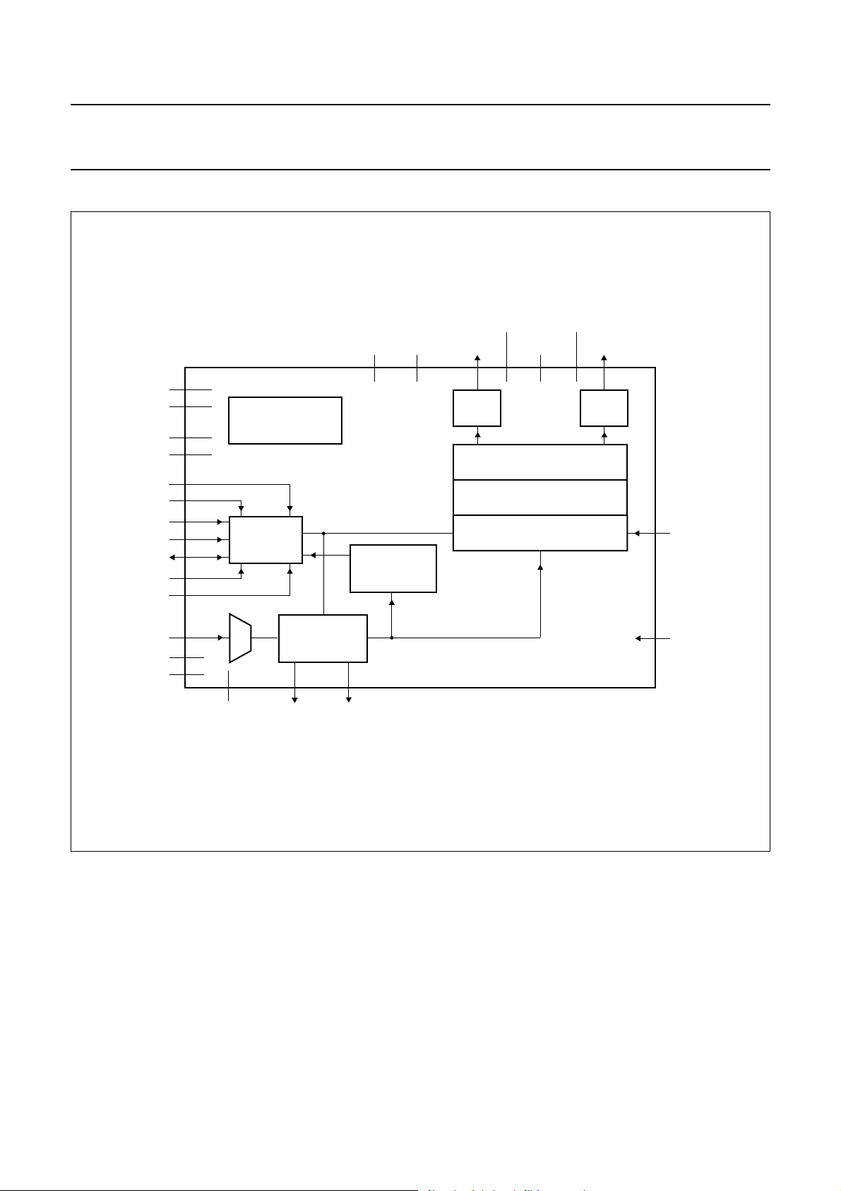
6 BLOCK DIAGRAM
handbook, full pagewidth
V
DDA(PLL)
V
SSA(PLL)
V
DDD(C)
V
SSD(C)
DA0
DA1
L3MODE
L3CLOCK
L3DATA
SELSTATIC
SELIIC
SPDIF
V
DDD
V
SSD
V
DDA(DAC)
V
TEST12TEST2
24
23
6
12
28
25
10
9
8
26
4
13
3
7
n.c.
CLOCK
TIMING CIRCUIT
L3-BUS
2
C-BUS
OR I
INTERFACE
SLICER
21, 22, 27
AND
IEC 60958
DECODER
1
PCMDET
UDA1352TS
NON-PCM DATA
SYNC
DETECTOR
16
LOCK
VOUTL
18
DAC
AUDIO FEATURE PROCESSOR
SSA(DAC)
14
15
NOISE SHAPER
INTERPOLATOR
V
ref
VOUTR
19
20
DAC
17
11
MGU655
MUTE
5
RESET
Fig.1 Block diagram.
2002 Nov 22 5
NXP Semiconductors Preliminary specification
48 kHz IEC 60958 audio DAC UDA1352TS
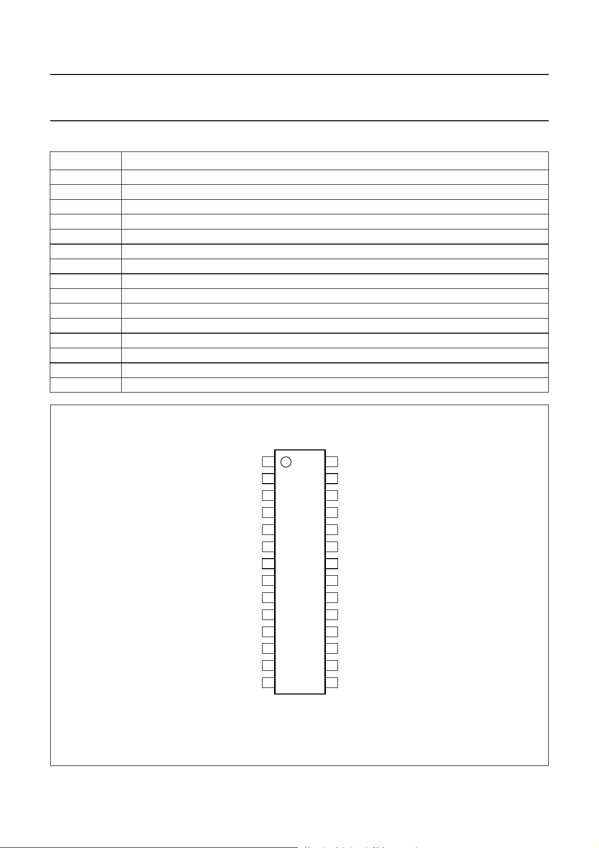
7 PINNING
SYMBOL PIN TYPE
(1)
DESCRIPTION
PCMDET 1 DO PCM detection indicator output
TEST1 2 DO test pin 1; must be left open-circuit in application
V
DDD
SELIIC 4 DID I
3 DS digital supply voltage
2
C-bus or L3-bus mode selection input
RESET 5 DID reset input
V
DDD(C)
V
SSD
L3DATA 8 IIC L3-bus or I
L3CLOCK 9 DIS L3-bus or I
6 DS digital supply voltage for core
7 DGND digital ground
2
C-bus interface data input and output
2
C-bus interface clock input
L3MODE 10 DIS L3 interface mode input
MUTE 11 DID mute control input
V
SSD(C)
12 DGND digital ground for core
SPDIF 13 AIO IEC 60958 channel input
V
DDA(DAC)
14 AS analog supply voltage for DAC
VOUTL 15 AIO DAC left channel analog output
LOCK 16 DO SPDIF and PLL lock ind i ca to r output
VOUTR 17 AIO DAC right channel analog output
TEST2 18 DID test pin 2; must be connected to digital ground (V
V
ref
V
SSA(DAC)
19 AIO DAC reference voltage
20 AGND analog ground for DAC
n.c. 21 − not connected
n.c. 22 − not connected
V
SSA(PLL)
V
DDA(PLL)
23 AGND analog ground for PLL
24 AS analog supply voltage for PLL
DA1 25 DISU A1 device address selection input
SELSTATIC 26 DIU static pin control selection input
n.c. 27 − not connected (reserved)
DA0 28 DID A0 device address selection input
) in application
SSD
Note
1. See Table 1.
2002 Nov 22 6
NXP Semiconductors Preliminary specification
48 kHz IEC 60958 audio DAC UDA1352TS
Table 1 Pin types
TYPE DESCRIPTION
DS digital supply
DGND digital ground
AS analog supply
AGND analog ground
DI digital input
DIS digital Schmitt-triggered input
DID digital input with internal pull-down resistor
DISD digital Schmitt-triggered input with internal pull-down resistor
DIU digital input with internal pull-up resistor
DISU digital Schmitt-triggered input with internal pull-up resistor
DO digital output
DIO digital input and output
DIOS digital Schmitt-triggered input and output
2
IIC input and open-drain output for I
AIO analog input and output
C-bus
handbook, halfpage
V
DDA(DAC)
PCMDET
TEST1
V
DDD
SELIIC
RESET
V
DDD(C)
V
SSD
L3DATA
L3CLOCK
L3MODE
MUTE
V
SSD(C)
SPDIF
1
2
3
4
5
6
7
UDA1352TS
8
9
10
11
12
13
14
MGU654
DA0
28
n.c.
27
SELSTATIC
26
DA1
25
V
24
V
23
n.c.
22
n.c.
21
V
20
V
19
TEST2
18
VOUTR
17
LOCK
16
VOUTL
15
DDA(PLL)
SSA(PLL)
SSA(DAC)
ref
Fig.2 Pin configuration.
2002 Nov 22 7

NXP Semiconductors Preliminary specification
48 kHz IEC 60958 audio DAC UDA1352TS
8 FUNCTIONAL DESCRIPTION
8.1 Clock regeneration and lock detection
The UDA1352TS contains an on-board PLL for
regenerating a system clock from the IEC 60958 input
bitstream.
Remark: If there is no input signal, the PLL generates a
minimum frequency and the output spectrum shifts
accordingly. Since the analog output does not hav e an
analog mute, this means noise that is out of band under
normal conditions can move into the audio band.
When the on-board clock locks to the incoming freq uency,
the lock indicator bit is set and can be read via the L3-bus
2
C-bus interface. Internally, the PLL lock indication can
or I
be combined with the PCM status bit of the input data
stream and the status whether any burst preamble is
detected or not. By default, when both the IEC 60958
decoder and the on-board clock have loc ke d to the
incoming signal and the input data stream is PCM data,
pin LOCK will be asserted. However, when the IC is locked
but the PCM status bit reports non-PCM data, pin LOCK is
returned to LOW level. This combination of the lock status
and the PCM detection can be overruled by the L3-bus or
2
C-bus register setting.
I
handbook, halfpage
1
mute
factor
0.8
0.6
0.4
0.2
0
01051525
Fig.3 Mute as a function of raised cosine roll-off.
MGU119
20
t (ms)
The lock indication output can be used, for example, for
muting purposes. The lock signal can be used to drive an
external analog muting circuit to prevent out of band noise
from becoming audible when the PLL runs at its minimum
frequency (e.g. when there is no SPDIF input signal).
The UDA1352TS has a dedicated pin PCMDET to indicate
whether valid PCM data stream is detected or (supposed
to be) non-PCM data is detected.
8.2 Mute
The UDA1352TS is equipped with a cosine roll-off mute in
the DSP data path of the DAC part. Muting the DAC (by
2
pin MUTE or via bit MT in the L3-bus or I
C-bus mode)
will result in a soft mute as shown in Fig.3. The cosine
roll-off soft mute takes 32 × 32 samples = 23 ms at
44.1 kHz sampling frequency.
2
When operating in the L3-bus or I
will mute on start-up. In the L3-bus or I
C-bus mode, the device
2
C-bus mode, it is
necessary to explicitly switch off the mute for audio output
by means of bit MT in the device register.
2
In the L3-bus or I
C-bus mode, pin MUTE will at all time
mute the output signal. This is in contrast to the UDA1350
and the UDA1351 in which pin MUTE in the L3-bus mode
does not have any function.
8.3 Auto mute
By default, the DAC outputs will be muted until the
UDA1352TS is locked, regardless of the level on
pin MUTE or the state of bit MT. In this way, only valid data
will be passed to the outputs. This mute is done in the
SPDIF interface and is a hard mute, not a cosine roll-off
mute.
If needed, this muting can be bypassed by setting
2
bit MUTEBP = 1 via the L3-bus or I
C-bus interface. As a
result, the UDA1352TS will no longer mute during
out-of-lock situations.
2002 Nov 22 8
NXP Semiconductors Preliminary specification
48 kHz IEC 60958 audio DAC UDA1352TS
8.4 Data path
The UDA1352TS data path consists of the IEC 60958
decoder, the audio feature processor, the digital
interpolator and noise shaper and the DACs.
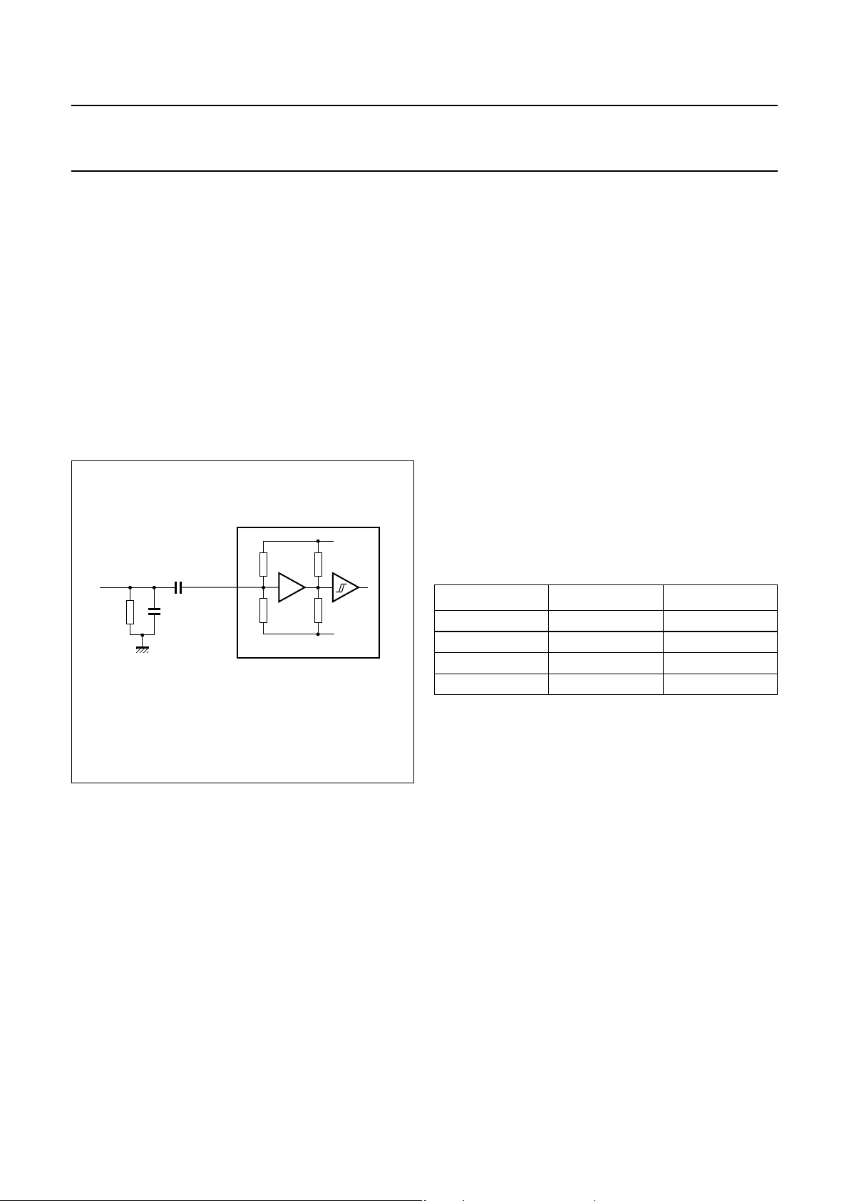
8.4.1 IEC 60958
INPUT
The IEC 60958 decoder features an on-chip amplifier with
hysteresis, which amplifies the SPDIF input signal to
CMOS level (see Fig.4).
All 24 bits of data for left and right are extracted from the
input bitstream as well as 40 channel status bits for left and
2
right. These bits can be read via the L3-bus or I
C-bus
interface.
handbook, halfpage
75 Ω
10 nF
180 pF
13SPDIF
UDA1352TS
MGU656
8.4.2 A
UDIO FEATURE PROCESSOR
The audio feature processor automatically prov ides
de-emphasis for the IEC 60958 data stream in the static
pin control mode and default mute at start-up in the L3-bus
2
C-bus mode.
or I
2
When used in the L3-bus or I
C-bus mode, it provides the
following additional features:
• Left and right independent volume control
• Bass boost control
• Treble control
• Mode selection of the sound processing bass boost and
treble filters: flat, minimum and maximum
• Soft mute control with raised cosine roll-off.
8.4.3 I
NTERPOLATOR
The UDA1352TS includes an on-board interpolating filter
which converts the incoming data stream from 1f
to 64fs
s
by cascading a recursive filter and a FIR filter.
Table 2 Interpolator characteristics
PARAMETER CONDITIONS VALUE (dB)
Pass-band ripple 0 to 0.45f
Stop band >0.55f
Dynamic range 0 to 0.45f
s
s
s
±0.03
−50
114
DC gain −−5.67
OISE SHAPER
Fig.4 IEC 60958 input circuit and typical
application.
8.4.4 N
The fifth-order noise shaper operates at 64fs. It shifts
in-band quantization noise to frequencies well abov e the
audio band. This noise shaping technique enables high
signal-to-noise ratios to be achieved. Th e noise shaper
The UDA1352TS supports the following sample
frequencies and data bit rates:
= 32.0 kHz, resulting in a data rate of 2.048 Mbits/s
• f
s
= 44.1 kHz, resulting in a data rate of 2.8224 Mbits/s
• f
s
• f
= 48.0 kHz, resulting in a data rate of 3.072 Mbits/s.
s
output is converted to an analog s ignal using a filter stream
DAC.
The UDA1352TS supports timing levels I, II and III, as
specified by the IEC 60958 standard. This means that the
accuracy of the above mentioned sampling frequencies
depends on the timing level I, II or III as mentioned in
Section 11.4.1.
2002 Nov 22 9
NXP Semiconductors Preliminary specification
48 kHz IEC 60958 audio DAC UDA1352TS
8.4.5 FILTER STREAM DAC
The Filter Stream DAC (FSDAC) is a semi-digital
reconstruction filter that converts the 1-bit data stream of
the noise shaper to an analog output voltage.
The filter coefficients are implemented as current sources
and are summed at virtual ground of the output operational
amplifier. In this way, very high signal-to-noise
performance and low clock jitter sensitivity is achieved.
A post filter is not needed due to the inherent filter function
of the DAC. On-board amplifiers convert the FSDAC
8.5 Control
The UDA1352TS can be controlled by means of static pins
2
(when pin SELSTATIC = HIGH), via the I
C-bus (when
pin SELSTATIC = LOW and pin SELIIC = HIGH) or via the
L3-bus (when pins SELSTATIC and SELIIC are LOW).
For optimum use of the features of the UDA1352TS, the
2
L3-bus or I
C-bus mode is recommended sinc e only basic
functions are available in the static pin control mode.
It should be noted that the st atic pi n contr ol mode and th e
2
L3-bus or I
C-bus mode are mutually exclusive.
output current to an output voltage signal capable of
driving a line output.
The output voltage of the FSDAC is scaled proportionally
with the power supply voltage.
8.5.1 S
The default values for all non-pin controlled settings are
identical to the default values at start-up in the L3-bus or
2
C-bus mode (see Table 3).
I
TATIC PIN CONTROL MODE
Table 3 Pin description of static pin control mode
PIN NAME VALUE FUNCTION
Mode selection pin
26 SELSTATIC 1 select static pin control mode; must be connected to V
DDD
Input pins
5 RESET 0 normal operation
1reset
9 L3CLOCK 0 must be connected to V
10 L3MODE 0 must be connected to V
8 L3DATA 0 must be connected to V
SSD
SSD
SSD
11 MUTE 0 no mute
1 mute active
Status pins
1 PCMDET 0 non- PCM data or burst preamble detected
1 PCM data detected
16 LOCK 0 clock regeneration and IEC 60958 decoder out-of-lock or non-PC M data detect ed
1 cloc k re generation and IEC 60958 decoder locked and PCM data detected
Test pins
2 TEST1 − must be left open-circuit
18 TEST2 0 must be connected to V
SSD
2002 Nov 22 10
NXP Semiconductors Preliminary specification
48 kHz IEC 60958 audio DAC UDA1352TS
8.5.2 L3-BUS OR I2C-BUS MODE
The L3-bus or I2C-bus mode allows maximum flexibility in controlling the UDA1352TS (see Table 4).
2
It should be noted that in the L3-bus or I
and that, on start-up in the L3-bus or I
interface.
C-bus mode, several base-line functions are still controlled by pins on the device
2
C-bus mode, the output is explicitly muted by bit MT via the L3-bus or I2C-bus
Table 4 Pin description in the L3-bus or I
2
C-bus mode
PIN NAME VALUE FUNCTION
Mode selection pins
2
26 SELSTATIC 0 select L3-bus mode or I
4 SELIIC 0 select L3-bus mode; must be connected to V
1select I2C-bus mode; must be connected to V
C-bus mode; must be connected to V
SSD
DDD
SSD
Input pins
5 RESET 0 normal operation
1 reset
8L3DATA − must be connec ted to the L3-bus
2
− must be connected to the SDA line of the I
C-bus
9 L3CLOCK − must be connected to the L3-bus
2
− must be connected to the SCL line of the I
C-bus
10 L3MODE − must be connected to the L3-b us
11 MUTE 0 no mute
1 mute active
Status pins
1 PCMDET 0 non-PCM data or burst preamble detected
1 PCM data detected
16 LOCK 0 clock regeneration and IEC 60958 decoder ou t-of-lock or non-PCM data detected
1 clock regeneration and IEC 60958 decoder locked and PCM data detected
Test pins
2 TEST1 − must be left open-circuit
18 TEST2 0 must be connected to V
SSD
2002 Nov 22 11
NXP Semiconductors Preliminary specification
48 kHz IEC 60958 audio DAC UDA1352TS
9 L3-BUS DESCRIPTION
9.1 General
The UDA1352TS has an L3-bus microcontroller interface
and all the digital sound processing features and various
system settings can be controlled by a microcontr olle r .
The controllable settings are:
• Restoring L3-bus default values
• Power-on
• Selection of filter mode and settings of treble and bass
boost
• Volume settings left and right
• Selection of soft mute via cosine roll-off and bypass of
auto mute.
The readable settings are:
• Mute status of interpolator
• PLL locked
• SPDIF input signal locked
• Audio sample frequency
• Valid PCM data detected
• Pre-emphasis of the IEC 60958 input signal
• Accuracy of the clock.
The exchange of data and control information between the
microcontroller and the UDA1352TS is LSB first and is
accomplished through the serial hardware L3-bus
interface comprising the following pins:
• L3DATA: data line
• L3MODE: mode line
• L3CLOCK: clock line.
The L3-bus format has two modes of operation:
• Address mode
• Data transfer mode.
The address mode is used to select a devi ce for a
subsequent data transfer. The address mode is
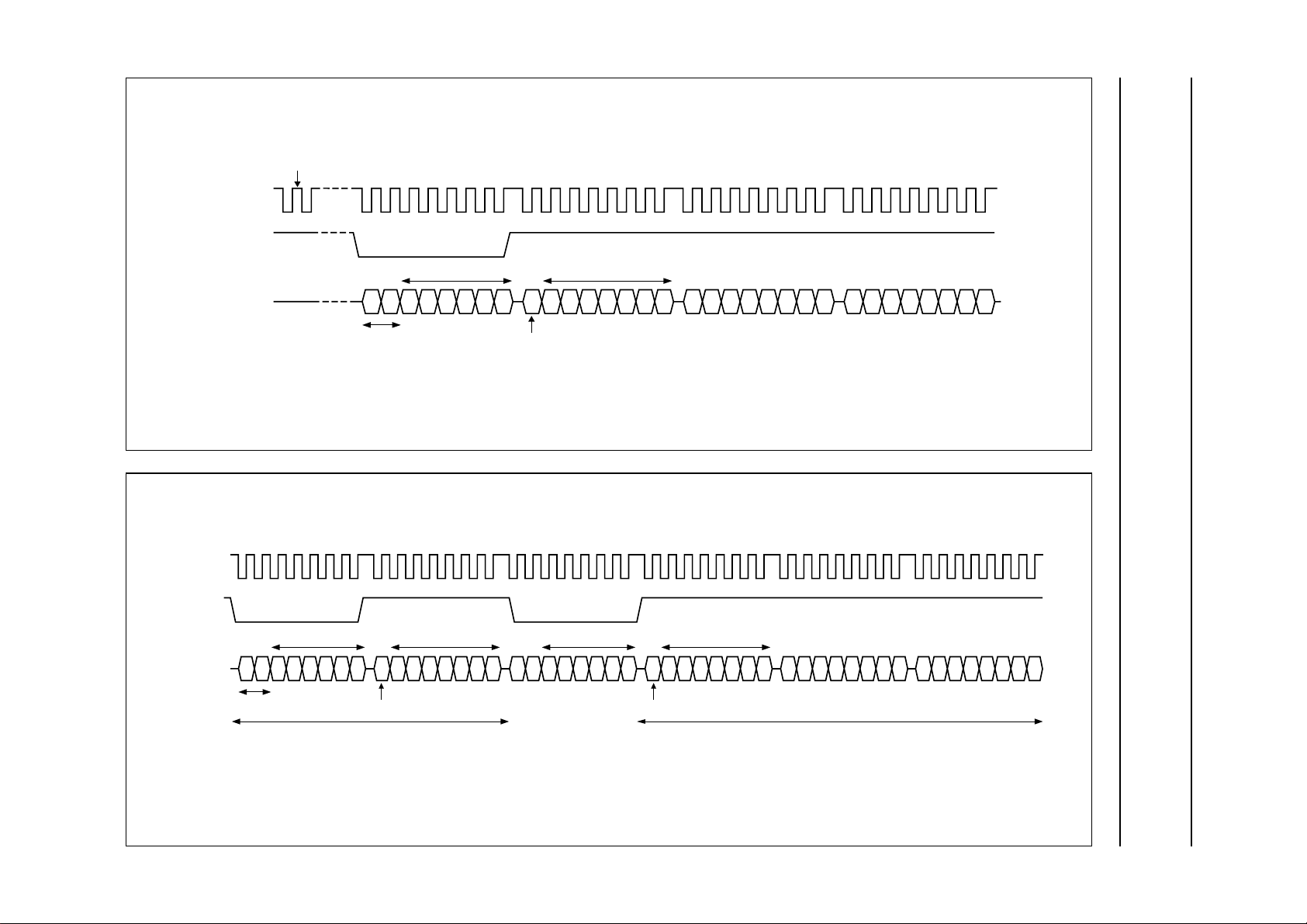
characterized by L3MODE being LOW and a burst of
8 pulses on L3CLOCK, accompanied by 8 bits (see Fig.5).
The data transfer mode is characterized by L3MODE
being HIGH and is used to transfer one or more bytes
representing a register address, instruction or data.
Basically, two types of data transfers can be defined:
• Write action: data transfer to the device
• Read action: data transfer from the device.
Remark: when the device is powered-up, at least one
L3CLOCK pulse must be given to the L3-bus interface to
wake-up the interface before starting sending to the device
(see Fig.5). This is only needed once after the device is
powered-up.
9.2 Device addressing
The device address consists of 1 byte with:
• Data Operating Mode (DOM) bits 0 and 1 representing
the type of data transfer (see Table 5)
• Address bits 2 to 7 representing a 6-bit device address.
The bits 2 and 3 of the address can be selected via the
external pins DA0 and DA1, which allows up to
4 UDA1352TS devices to be independently controlled in
a single application.
The primary address of the UDA1352TS is ‘001000’ (LSB
to MSB) and the default address is ‘011000’.
Table 5 Selection of data transfer
DOM
TRANSFER
BIT 0 BIT 1
0 0 not used
1 0 not used
0 1 write data or prepare read
11read data
9.3 Register addressing
After sending the device address (including DOM bits),
indicating whether the information is to be read or written,
one data byte is sent using bit 0 to indicate whether the
information will be read or written and bits 1 to 7 for the
destination register address.
Basically, there are three methods for register addressing:
1. Addressing for write data: bit 0 is logic 0 indicating a
write action to the destination register, followed by bits
1 to 7 ind i cating the register address (see Fig.5)
2. Addressing for prepare read: bit 0 is logic 1, indicating
that data will be read from the register (see Fig.6)
3. Addressing for data read action. Here, the device
returns a register address prior to sending data from
that register. When bit 0 is logic 0, the register address
is valid; when bit 0 is logic 1, the register address is
invalid.
2002 Nov 22 12
2002 Nov 22 13
3
L
5
L
L
L
NXP Semiconductors Preliminary specification
48 kHz IEC 60958 audio DAC UDA1352TS
L3 wake-up pulse after power-up
3CLOCK
L3MODE
L3DATA
device address
10
0
DOM bits
write
Fig.5 Data write mode (for L3-bus version 2).
register address
data byte 1 data byte 2
MGS75
3CLOCK
3MODE
3DATA
DOM bits
device address
111
0
prepare read sent by the device
register address device address
1
read
valid/invalid
Fig.6 Data read mode.
register address
0/1
requesting
data byte 1 data byte 2
MBL56
NXP Semiconductors Preliminary specification
48 kHz IEC 60958 audio DAC UDA1352TS
9.4 Data write mode
The data write mode is explained i n th e signal diagram of
Fig.5. For writing data to a device, 4 bytes must be sent
(see Table 6):
1. One byte starting with ‘01’ for signalling the write
action to the device, followed by the device address
(‘011000’ for the UDA1352TS default)
2. One byte starting with a ‘0’ for signalling the write
action, followed by 7 bits indicating the destination
register address in binary format with A6 being the
MSB and A0 being the LSB
3. One data byte (from the two data bytes) with D15
being the MSB
4. One data byte (from the two data bytes) with D0 being
the LSB.
It should be noted that each time a new destination register
address needs to be written, the device address mus t be
sent again.
9.5 Data read mode
To read data from the device, a prepare read must first be
done and then data read. The data read mode is explained
in the signal diagram of Fig.6.
For reading data from a device, the following 6 bytes are
involved (see Table 7):
1. One byte with the device address, including ‘01’ for
signalling the write action to the device
2. One byte is sent with the register address from which
data needs to be read; this byte st arts with a ‘1’, which
indicates that there will be a read action from the
register, followed by seven bits for the source register
address in binary format, withA6 being the MSB
and A0 being the LSB
3. One byte with the device address preceded by ‘11’ is
sent to the device; the ‘11’ indicates that the device
must write data to the microcontroller
4. One byte, sent by the device to the bus, with the
(requested) register address and a flag bit ind icating
whether the requested register was valid (bit is logic 0)
or invalid (bit is logic 1)
5. One byte (from the two bytes), sent by the device to
the bus, with the data information in binary format,
with D15 being the MSB
6. One byte (from the two bytes), sent by the device to
the bus, with the data information in binary format,
with D0 being the LSB.
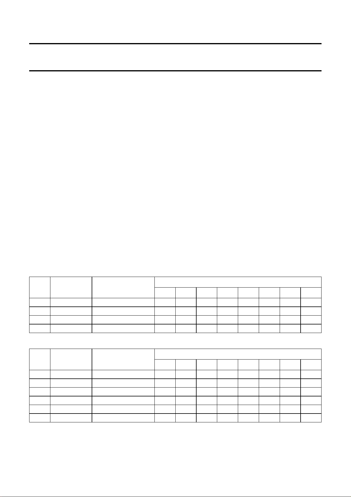
Table 6 L3-bus write data
BYTE
1address device address 01DA0DA11000
2 data transfer register address 0 A6 A5 A4 A3 A2 A1 A0
3 data transfer data byte 1 D15 D14 D13 D12 D11 D10 D9 D8
4 data transfer data byte 2 D7 D6 D5 D4 D3 D2 D1 D0
Table 7 L3-bus read data
BYTE
1address device address 01DA0DA11000
2 data transfer register address 1 A6 A5 A4 A3 A2 A1 A0
3address device address 11DA0DA11000
4data transferregister address 0or1A6A5A4A3A2A1A0
5 data transfer data byte 1 D15 D14 D13 D12 D11 D10 D9 D8
6 data transfer data byte 2 D7 D6 D5 D4 D3 D2 D1 D0
L3-BUS
MODE
L3-BUS
MODE
ACTION
ACTION
FIRST IN TIME LAST IN TIME
BIT 0 BIT 1 BIT 2 BIT 3 BIT 4 BIT 5 BIT 6 BIT 7
FIRST IN TIME LAST IN TIME
BIT 0 BIT 1 BIT 2 BIT 3 BIT 4 BIT 5 BIT 6 BIT 7
2002 Nov 22 14
NXP Semiconductors Preliminary specification
48 kHz IEC 60958 audio DAC UDA1352TS
9.6 Initialization string
For proper and reliable operation, the UDA1352TS must be initialized in the L3-bus mode. This is required to have the
PLL start-up after powering up of the device under all conditions. The initialization string is given in Table 8.
Table 8 L3-bus initialization string and set defaults after power-up
BYTE
L3-BUS
MODE
ACTION
FIRST IN TIME LAST IN TIME
BIT0 BIT1 BIT2 BIT3 BIT4 BIT5 BIT6 BIT7
1 address init string device address 0 1 DA0 DA1 1 0 0 0
2data transfer register address01000000
3data transfer data byte1 00000000
4data transfer data byte2 00000001
5 address set
6data transfer register address01111111
defaults
device address 0 1 DA0 DA1 1 0 0 0
7data transfer data byte1 00000000
8data transfer data byte2 00000000
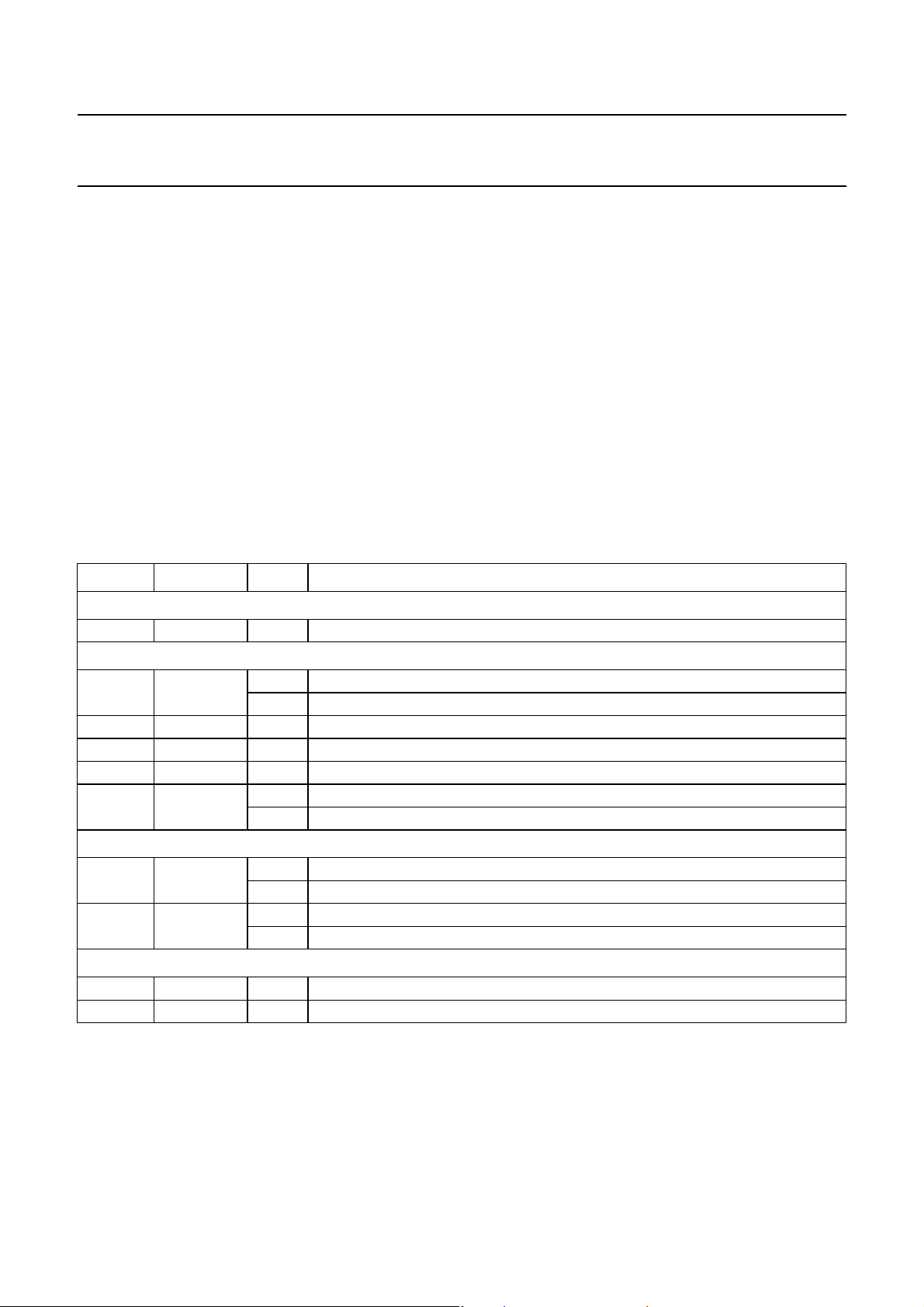
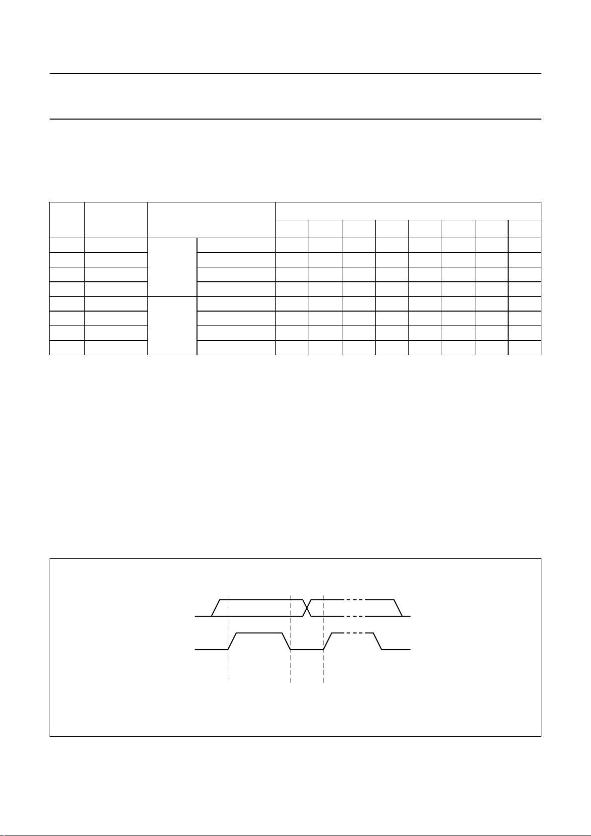
10 I2C-BUS DESCRIPTION
10.1 Characteristics of the I
2
C-bus
10.2 Bit transfer
One data bit is transferred during each clock pulse (see
Fig.7). The data on the SDA line must remain stable during
The bus is for 2-way, 2-line communication between
different ICs or modules. The two lines are a serial data
line (SDA) and a serial clock line (SCL). Both lines must be
connected to the V
via a pull-up resistor when
DD
connected to the output stages of a microcontroller. For a
400 kHz IC the recommendation for this type of bus from
NXP Semiconductors must be followed (e.g. up to loads of
200 pF on the bus a pull-up resistor can be used, between
the HIGH period of the clock pulse as changes in the data
line at this time will be interpreted as control signals. The
maximum clock frequency is 400 kHz.
To be able to run on this high frequenc y all the in puts an d
outputs connected to this bus must be designed for this
2
high-speed I
2
C-bus and how to use it”, (order code 9398 393 40011).
I
C-bus according to specification “The
200 to 400 pF a current source or switched resistor must
be used). Data transfer can only be initiated when the bus
is not busy.
handbook, full pagewidth
SDA
SCL
data line
stable;
data valid
change
of data
allowed
MBC621
Fig.7 Bit transfer on the I2C-bus.
2002 Nov 22 15
NXP Semiconductors Preliminary specification
48 kHz IEC 60958 audio DAC UDA1352TS
10.3 Byte transfer
Each byte (8 bits) is transferred with the MSB first
(see Table 9).
Table 9 Byte transfer
MSB BIT NUMBER LSB
76543210
10.4 Data transfer
A device generating a message is a transmitter, a device
receiving a message is the receiver. The device that
handbook, full pagewidth
SDA
SCL
S
controls the message is the maste r and the devic es which
are controlled by the master are the slaves.
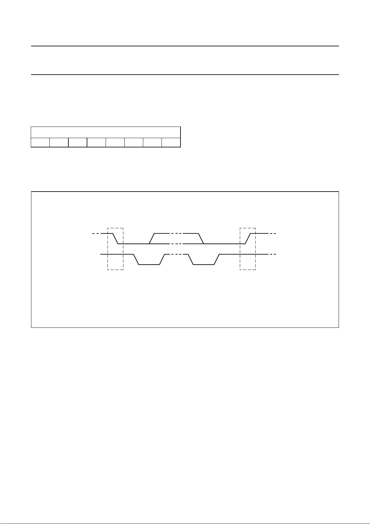
10.5 Start and stop conditions
Both data and clock line will remain HIGH when the bus is
not busy. A HIGH-to-LOW tran sition of the data lin e, while
the clock is HIGH, is defined as a start condition (S);
see Fig.8. A LOW-to-HIGH transition of the data line while
the clock is HIGH is defined as a stop condition (P).
SDA
SCL
P
START condition
Fig.8 START and STOP conditions on the I2C-bus.
10.6 Acknowledgment
The number of data bits transferred betw een the start and
stop conditions from the transmitter to receiver is not
limited. Each byte of eight bits is followed by one
acknowledge bit (see Fig.9). At the acknowledge bit the
data line is released by the master and the master
generates an extra acknowledge related clo ck pulse.
A slave receiver which is addressed must generate an
acknowledge after the reception of each byte. Also a
master must generate an acknowledge after the reception
of each byte that has been clocked out of the slave
transmitter.
STOP condition
MBC622
The device that acknowledges has to pull-down the SDA
line during the acknowledge clock pulse, so that the SDA
line is stable LOW during the HIGH period of the
acknowledge related clock pulse. Set-up and hold times
must be taken into account. A master receiver must signal
an end of data to the transmitter by not generating an
acknowledge on the last b yte that h as been cloc ked out of
the slave. In this event, the transmitter must leave the data
line HIGH to enable the master to generate a stop
condition.
2002 Nov 22 16
 Loading...