

Page 1

TWR-56F8400
User Manual
Rev. O.01
Freescale Semiconductor Inc.
Microcontroller Solutions Group
Page 2

Contents
Overview .......................................................................................................................................................... 4
1.1 Block Diagram ...................................................................................................................................................................... 5
1.2 Reference Documents ....................................................................................................................................................... 5
2 Hardware Features ................................................................................................................................... 6
2.1 Tower MCU Module ........................................................................................................................................................... 6
2.2 System Power ....................................................................................................................................................................... 6
2.2.1 P5V_USB ................................................................................................................................................................................................. 6
2.2.2 P3_3V ....................................................................................................................................................................................................... 6
2.2.3 P3_3V/5V ............................................................................................................................................................................................... 7
2.2.4 Default Power Configuration ........................................................................................................................................................ 7
2.3 MC56F84789 DSC ............................................................................................................................................................... 7
2.3.1 Clock Sources for the MC56F84789 DSC ................................................................................................................................. 7
2.3.2 Serial I/O Source Select Headers ................................................................................................................................................. 8
2.3.3 LEDs Controlled by the MC56F84789 DSC ............................................................................................................................. 9
2.3.4 Motor Control Connector ............................................................................................................................................................. 10
2.3.5 Auxiliary Connectors ..................................................................................................................................................................... 11
2.3.6 Tower Elevator Connectors ........................................................................................................................................................ 14
2.3.7 Thermistors as Analog Inputs ................................................................................................................................................... 14
2.3.8 CAN Transceiver .............................................................................................................................................................................. 14
2.3.9 IRQ or Input Pushbuttons ............................................................................................................................................................ 15
2.3.10 RESET ................................................................................................................................................................................................ 15
2.3.11 JTAG Header and OSBDM/OSJTAG Disconnect Header ............................................................................................... 15
2.4 OSBDM/OSJTAG ............................................................................................................................................................... 16
2.4.1 Debug Interface ................................................................................................................................................................................ 16
2.4.2 USB Serial Bridge Interface ......................................................................................................................................................... 16
2.4.3 Clocking the OSBDM/OSJTAG MCU (MC9S08JM60) ........................................................................................................ 16
2.4.4 OSBDM/OSJTAG/UART Function Select Header ............................................................................................................... 16
2.4.5 Bootloader Enable .......................................................................................................................................................................... 17
2.4.6 BDM Header ....................................................................................................................................................................................... 17
2.4.7 OSBDM/OSJTAG Status LEDs ..................................................................................................................................................... 17
2.4.8 OSBDM/OSJTAG Voltage Translation ..................................................................................................................................... 17
3 Jumper Table ........................................................................................................................................... 18
Appendix A – Tower Elevator Connector Pin Functions .............................................................. 20
Appendix B – TWR-56F8400 Board Schematic ............................................................................... 23
Appendix C – TWR-56F8400 Board BOM .......................................................................................... 24
Appendix D – TWR-56F8400 Board Jack Layout Top View ............................................................ 1
TWR-56F8400 User’s Manual Page 2 of 35
Page 3

JLW Ported from MC56F8257 to the 32-bit MC56F84789
Revision History
Revision Date Changes
O 12 Dec 2009 Input from Jay Hartvigsen
O.01 4 Jan 2010 Update from Jay Hartvigsen
Reordered list of features in overview to match the table of
contents order. Correction to Table 2. Added LED Label
column in table 3. Added requested comment on CAN TXD
and RXD nets – that they also go to the elevator connector.
O.02 21 Jan 2010
O.03 29 Jan 2010 Updated document list in section 1.2 by Petr Stekl
Improved description of USB Serial Bridge Interface and
moved the circuit description of this interface from section
2.3.2 to section 2.4.2. Added Tower Elevator Connector
table. Added an appendix to put the schematic in. Added
BOM.
0.00
0.01
0.02 6 March 2012 JLW corrections to composite signal names
0.03 6 March 2012
0.04 7 March 2012 JLW added back schematic as rev B
25 February
2012
27 February
2012
Note: OSBDM implies “also OSJTAG” below.
Due to the tight layout, added appendix for layout of
headers used for jumpers to aid in their identification.
JLW responded to customer feedback as well as Ankar
feedback.
JLW removed schematic. Editor to embed schematic as
object. Corrected TOWER signal names per latest. Included
new functionality of S08 firmware for CDC serial port.
Released to publications.
TWR-56F8400 User’s Manual Page 3 of 35
Page 4

Overview
The MC56F8400 Tower 32-bit MCU Module (TWR-56F8400) is an evaluation, demonstration and
development board. The TWR-56F8400 can operate stand-alone or as the main control board in a
Tower system with peripheral modules. It can also be used as the main control board with an
APMOTOR56F8000E motor control board.
The following list summarizes the features of the TWR-56F8400:
• 32 bit Digital Signal Controller module featuring MC56F84789
• Tower compatible
• Selectable Power sources:
o USB on 56F8400 card
o Barrel connector on 56F8400 card
o Motor control board plug direct to 56F8400 card, no Tower connection, plug Motor
control to nine volts
o Tower elevator board (USB or Barrel on Primary side)
• Filtered power for VDDA and VSSA on the 32-bit MC56F84789DSC
• MC56F84789 DSC (Digital Signal Controller) in an 100 LQFP package
• Optional 8 MHz crystal circuit for the MC56F84789 DSC
• 9 LEDs controlled by the MC56F84789 DSC
• Motor Control Board connector for the APMOTOR56F8000E motor control board
• Auxiliary Signal connector
• Four Thermistors for single ended or differential analog inputs to the MC56F84789 DSC
• CAN transceiver, header, and termination
• Two push buttons for user input or interrupts to the MC56F84789 DSC
• Reset push button for the MC56F84789 DSC
• JTAG header for the MC56F84789 DSC with header to disconnect from OSBDM/OSJTAG
• Headers to connect SCI signals to either USB bridge with CDC(one channel) or elevator board
(two channels) or connect one to each
• Expansion via Primary Elevator connector
• MC9S08JM60 (‘JM60) MCU with a 4 MHz crystal provides:
o Open Source Debug (OSBDM/OSJTAG) circuit
o USB to SCI bridge with CDC and other techniques supported by third parties
o Simultaneious OSBDM/OSJTAG and USB to SCI bridge functions with no header required
to select
o Bootloader enable header allows easy upgrade to latest S08 firmware pushed down by
CodeWarrior
o BDM header for the MC9S08JM60 MCU
o Status and Target Power indicator LEDs
o Control of semiconductor switch to enable power to board from USB
TWR-56F8400 User’s Manual Page 4 of 35
Page 5
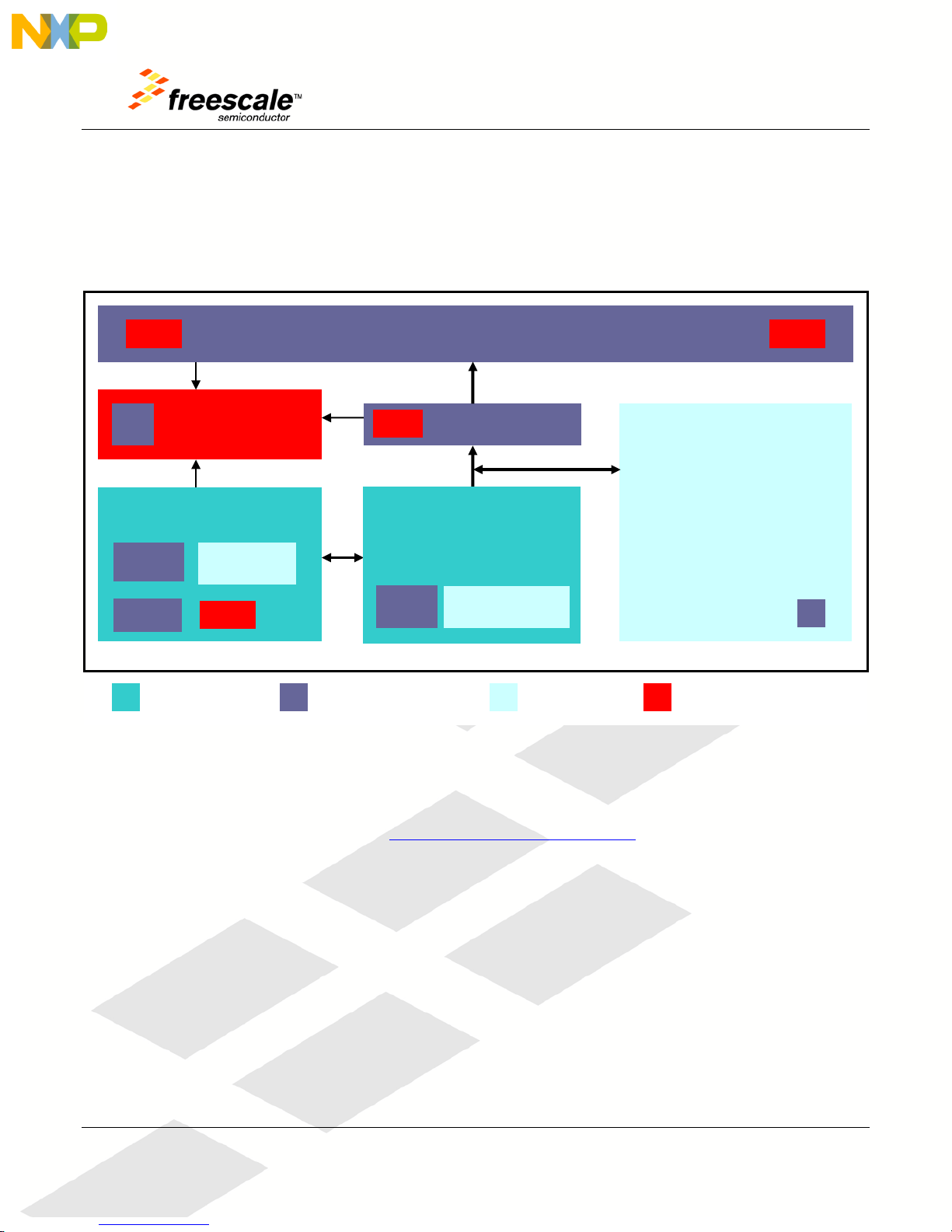
Motor Control&
Aux Connectors
(SPI, I2C, ADC, FEC, TPM, SCI, KB, etc.)
5.0V
3.3V
Freescale Device
External Connectors
Interface Circuits
Power
OSBDM (MC9S08JM60 MCU
Debug, Power, SCI Headers)
5.0V
USB
Mini-AB
Voltage
BDM
Header
Barrel Power Connector
5V-
MC56F84789
JTAG
Boot load HDR
o Voltage translators between 5V MC9S08JM60 MCU chip and 3.3V MC56F84789 DSC
chip
1.1 Block Diagram
A block diagram for the TWR-56F8400 is shown in Figure 1 below.
Tower Elevator Expansion Connectors
Power Selection HDRs
9V
Voltage Regulator
3.3V
• LEDs & Buffers (9)
• IRQ PB & HDRs (2)
• RESET PB
Digital Signal Controller
Translators
• Thermistors & HDRs (4)
• Analog Filters
• Microphone (optional)
Header
• CAN XCVR & HDR
Figure 1. TWR-56F8400 Block Diagram
1.2 Reference Documents
The documents listed below should be referenced for more information on the Freescale Tower
system and the TWR-56F8400. Refer to http://www.freesale.com/tower for the latest revision of all
Tower documentation.
• Freescale Tower Electromechanical Specification
• TWR-56F8400 Quick Start Guide
• TWR-56F8400 Lab Tutorials
• MC56F84XXX Reference Manual
• MC56F84XXX Data Sheet
• MC56F84XXX Chip Errata [if exists]
• AN3561, USB Bootloader for the MC9S08JM60
• Serial Bootloader for MC56F84XXX User Guide
• APMOTOR56F8000e Motor Control Demonstration System User Manual
TWR-56F8400 User’s Manual Page 5 of 35
Page 6

2 Hardware Features
This section provides more details about the features and functionality of the TWR-56F8400.
A drawing of the TWR-56F8400 showing the jack locations is shown in Appendix D. Features are
discussed below.
2.1 Tower MCU Module
The TWR-56F8400 board is an MCU Module designed for standalone use (or with a Freescale Tower
system) and complies with the electrical and mechanical specification as described in Freescale Tower
Electromechanical Specification. Connection to the Tower system is through two expansion card-edge
connectors that interface to the Elevator boards in a Tower system: the Primary and Secondary
Elevator connectors. The Primary Elevator connector, comprised of sides A and B, is utilized by the
TWR-56F8400, while the Secondary Elevator connector only makes connections to ground (GND). On
sheet 8 of the schematic the J500A and J500B symbols have names assigned to the card edge fingers
that correspond with the normal Tower pin assignments.
2.2 System Power
The TWR-56F8400 board has three power rails. They are P5V_USB, P3_3V and P3_3V/5V. They are
sourced and used as follows:
2.2.1 P5V_USB
The P5V_USB power rail is derived from the Mini-B USB connector at J18 and the inductor at L2. It is
used to power the on board OSBDM/OSJTAG/Serial Bridge circuit. This consists of the OSBDM/OSJTAG
MCU at U6, several pull-up resistors at R13, R14, R15, R527, and R528, the USB power switch at U501,
and the STATUS and TPWR LEDs at D12 and D13. If there is no USB cable connected to J18 there is no
power on this rail and these circuits are all powered down.
2.2.2 P3_3V
The P3_3V power rail is derived from a) the P3_3V_MOTOR power net from the motor control board
connector at J501, b) the P3_3V_ELEV power net from the tower connector at J500, or c) the on board
3.3V regulator at U1. The selection of which source is made with a shunt from J7-2 to another pin of J7
or to J6. Table 6 shows the operation of the different shunt positions. The selection of power into the
regulator is made with a shunt from J11-2 to another pin of J11 or to J10 which selects from a) the
P5V_TRG_USB power net out of the USB switch at U501, b) the P5V_ELEV power net from the elevator
connection at J500 pins A1 and B1, or c) the PWR_IN power net from the 2mm barrel jack at J3 through
resettable fuse F1. Table 6 shows the operation of the different shunt positions. The barrel jack input is
protected from reverse voltage inputs by diode D11. The input to the barrel jack may be from a 5V to
9V source and needs to be center positive.
TWR-56F8400 User’s Manual Page 6 of 35
Page 7

The P3_3V power rail provides power to the majority of the circuits on the board including the
MC56F84789 (including the analog power pins through L500 and L501), inverters at U500 and U502, a
buffer at U505, the on board LEDs at D1-D9, the thermistor divider circuits at RT1-RT4, and the pull-up
resistors at R2, R3, R11, R565, R570, and R562.
2.2.3 P3_3V/5V
The P3_3V/5V power rail is derived from the diode OR (using D500 and D501) of a) the P5V_ELEV
power net from the elevator connection (J500 pins A1 and B1), b) the P5V output of the USB power
switch at U501, or c) the P3_3V power rail from J7. When there is a USB cable connected or when the
tower elevator boards are connected this power rail will be a Schottky diode drop (about 0.3V) below
the 5V power nets. When there is no 5V source this power rail will be a Schottky diode drop below the
P3.3V power rail. This allows the inputs of the ICs powered by this rail to stay in a high impedance state
instead of loading down the inputs through the input protection diodes as would happen if there were
no power supplied to the buffers.
2.2.4 Default Power Configuration
The TWR-56F8400 board default power configuration uses the OSBDM/OSJTAG USB port for all power.
As soon as the OSBDM/OSJTAG firmware has started it negotiates with the Host PC USB port for full
USB power. Once approved it enables the 5V USB power switch (U501) which provides 5V to the
P3_3V/5V power rail and to the 3.3V regulator (U1) through headers J10 and J11. Likewise, the on
board voltage regulator provides 3.3V to the P3_3V power rail through headers J6 and J7. The 3.3V
regulator is able to provide up to 700 mA subject to the power dissipation and temperature limits of
the device.
2.3 MC56F84789 DSC
The primary circuits on the board are related to the MC56F84789 DSC. This part is supplied in a surface
mounted 100pin LQFP package at U2. Although the board was laid out to allow a ZIF socket at U3 in
parallel to the chip at U2 the TWR-56F8400 is only available for purchase with the surface mounted
chip.
2.3.1 Clock Sources for the MC56F84789 DSC
Three options are provided for clocking the MC56F84789 device:
1. Oscillator internal to the MC56F84789 chip – approximately 8 MHz.
2. 8 MHz crystal
3. External clock input from Primary Tower Connector or the AUX Connector.
The internal oscillator is used to clock the MC56F84789 immediately following reset. This is the default
operation. In this mode the zero ohm resistors at R4 and R10 allow the GPIOC0 and GPIOC1 pins of the
MC56F84789 to be used as inputs or outputs.
TWR-56F8400 User’s Manual Page 7 of 35
Page 8

2
GPIOF8/RXD0/TB1 from the 56F84789
To use an external crystal with the MC56F84789, zero ohm resistors R4 and R10 must be removed and
placed in the R5 and R7 positions. The desired crystal, load capacitors, and parallel resistor (if needed)
must be soldered to the board at Y1, C5, C6, and R6. (These components are not provided with the
TWR-56F8400 kit.) Following reset, reconfigure the GPIOC0 and GPIOC1 pins to the XTAL and EXTAL
functions to allow the use of an external crystal.
To use an external clock for the MC56F84789 make sure the zero ohm resistors are installed at R4 and
R10 and removed from R5 and R7. Provide a clock signal on either the Primary Tower Connector J500A
- pin B24 (the pin designated as CLOCKIN0) or on the AUX connector J502 - pin 8. Following reset,
configure the GPIOC0 pin to the CLKIN input function. In this mode the zero ohm resistor at R10 allows
the GPIOC1 pin of the MC56F84789 (pin 10) to be used as an input or output.
2.3.2 Serial I/O Source Select Headers
The TWR-56F8400 board allows the UART functions of the MC56F84789 DSC to be connected to a
serial interface at the primary Tower Connector J500A or through a USB bridge to the Host PC using the
OSBDM/OSJTAG MCU (U6). The selection of the RXD connections is done with the header at J8 as
shown in Table 1. The selection of the TXD connections is done with the header at J9 as shown in Table
2.
Table 1. J8 – RXD Source Select Header
J8 – RXD Source Select Header
Pin # Connected Signal Description
1 ELEV_RXD0 at J500A pin A41 Shunt pins 1 and 2 together to connect the DSC
RXDO pin to the primary Tower Connector RXD0
pin. (This is a default position.)
DSC – pin 6 (RXD0 function)
3 RXD_SEL from the USB bridge
function on the OSBDM/OSJTAG
MCU.
4 GPIOF5/RXD1/XB_OUT5 from the
56F84789 DSC – pin 42 (RXD1
function)
5 ELEV_RXD1 at J500 pin A43 Shunt pins 4 and 5 together to connect the DSC
Shunt pins 2 and 3 together to connect the DSC
RXD0 pin to the USB serial bridge function.
Shunt pin 3 and 4 together to connect the DSC
RXD1 pin to the USB serial bridge function.
RXD1 pin to the primary Tower Connector RXD1
pin. (This is a default position.)
TWR-56F8400 User’s Manual Page 8 of 35
Page 9

Table 2. J9 – TXD Source Select Header
J9 – TXD Source Select Header
Pin # Connected Signal Description
1 ELEV_TXD0 at J500A pin A42 Shunt pins 1 and 2 together to connect the DSC
TXDO pin to the primary Tower Connector TXD0
pin. (This is a default position.)
2 GPIOC2/TXD0/TB0/XB_IN2/CLKO
from the 56F84789 DSC – pin 5 (TXD0
function)
3 TXD_SEL to the USB bridge function
on the OSBDM/OSJTAG MCU.
4 GPIOF4/TXD1/XB_OUT4 from the
56F84789 DSC – pin 41 (TXD1
function)
5 ELEV_TXD1 at J500 pin A44 Shunt pins 4 and 5 together to connect the DSC
As can be seen in the tables the 56F84789 DSC serial signals may be connected to either the Tower
serial signals or to the USB bridge chip; however, only one channel may be connected to the USB
bridge chip. If the associated 56F84789 DSC serial pins are not being used for the serial functions the
shunts should be removed from those pins. For more information on the USB Serial Bridge function see
section 2.4.2 USB Serial Bridge Interface.
Shunt pins 2 and 3 together to connect the DSC
TXD0 pin to the USB serial bridge function.
Shunt pin 3 and 4 together to connect the DSC
TXD1 pin to the USB serial bridge function.
TXD1 pin to the primary Tower Connector TXD1
pin. (This is a default position.)
2.3.3 LEDs Controlled by the MC56F84789 DSC
There are nine LEDs with buffers connected to the MC56F84789 DSC. Inverting buffers (U500A-F and
U502D-F) isolate the LEDs from the DSC pins by providing high impedance inputs. The LEDs are
powered by the P3_3V rail and draw about 5mA each. Table 3 shows the DSC pin names associated
with each LED.
Table 3. LEDs Controlled by the MC56F84789 DSC
LEDs Controlled by the MC56F84789 DSC
MC56F84789 DSC
Pin Name
GPIOE0/PWMA_0B 68 D1 E0 Green
GPIOE1/PWMA_0A 69 D2 E1 Yellow
GPIOE2/PWMA_1B 74 D3 E2 Green
GPIOE3/PWMA_1A 75 D4 E3 Yellow
TWR-56F8400 User’s Manual Page 9 of 35
MC56F84789
Pin Number
LED
Reference
LED
Label
LED
Color
Page 10
GPIOE4/PWMA_2B/XB_IN2 82 D5 E4 Green
GPIOE5/PWMA_2A/XB_IN3 83 D6 E5 Yellow
GPIOE6/PWMA_3B/XB_IN4/PW
MB_2B
GPIOE7/PWMA_3A/XB_IN5/PW
MB_2A
GPIOF6/TB2/PWMA_3X/PWMB_
3X/XB_IN2
84 D7 E6 Green
85 D8 E7 Yellow
94 D9 F6 Amber
2.3.4 Motor Control Connector
The TWR-56F8400 board may be connected to a motor control board such as the APMOTOR56F8000E.
The motor control connector (J501) is on the bottom of the board to provide a convenient connection
to the motor control board.
Some of the MC56F84789 DSC pins are connected to the motor control connector. Those pins
associated with analog inputs have 100 ohm resistors in series to provide some ESD protection for the
analog inputs of the DSC. Those pins providing analog signals from the motor control board have 2200
pf caps with the resistors to provide a low pass filter. The connector pin out is shown in Table 4.
Table 4. Motor Control Connector Pin Out
Motor Control Connector J501 Pin Out
Pin
#
1 P3_3V_MOTOR 2 GPIOB7/ANB7&ANC15&CMPB_IN2
3 GND 4 RESETB/ GPIOD4
5 GPIOF4/TXD1/XB_OUT8 6 GPIOA3/ANA3&VREFLA&CMPA_IN2
7 GPIOF3/SDA1/XB_OUT7 8 GND
9 GPIOE1/PWMA_0A 10 GPIOA0/ANA0&CMPA_IN3/CMPC_O
11 GPIOE0/PWMA_0B 12 GPIOA1/ANA1&CMPA_IN0
13 GPIOC3/TA0/CMPA_O/RXD0/CLKIN1 14 GPIOA2/ANA2&VREFHA&CMPA_IN1
15 GPIOC13/TA3/XB_IN6/EWM_OUT_B 16 GND
MC56F84789 DSC Signal Pin
#
MC56F84789 DSC Signal
(With 100 ohms in series)
(With 0 ohms in series – remove to
isolate)
(With 100 ohms in series)
(With 100 ohm, 2200 pf low pass filter)
(With 100 ohm, 2200 pf low pass filter)
(With 100 ohm, 2200 pf low pass filter)
TWR-56F8400 User’s Manual Page 10 of 35
Page 11
Motor Control Connector J501 Pin Out
Pin
#
17 GPIOC4/TA1/CMPB_O/XB_IN8/EWM_OUT_B 18 GPIOB0/ANB0&CMPB_IN3
19 GPIOC6/TA2/XB_IN3/CMP_REF 20 GPIOB1/ANB1&CMPB_IN0
21 GPIOC15/SCL0/XB_OUT5 22 GPIOB2/ANB2&VREFHB&CMPC_IN3
23 GPIOC14/SDA0/XB_OUT4 24 GND
25 TDI /GPIOD0 26 GPIOE7/PWMA_3A/XB_IN5/PWMB_2A
27 TDO/ GPIOD1 28 GPIOE6/PWMA_3B/XB_IN4/PWMB_2B
29 TCK/GPIOD2 30 GPIOE3/PWMA_1A
31 TMS /GPIOD3 32 GPIOE2/PWMA_1B
33 GPIOB3/ANB3&VREFLB&CMPC_IN0
35 GPIOB4/ANB4&ANC12&CMPC_IN1
37 GPIOB5/ANB5&ANC13&CMPC_IN2
39 GPIOB6/ANB6&ANC14&CMPB_IN1
MC56F84789 DSC Signal Pin
#
34 GPIOE5/PWMA_2A/XB_IN3
(With 100 ohms in series)
36 GPIOE4/PWMA_2B/XB_IN2
(With 100 ohms in series)
38 GPIOA4/ANA4&ANC8&CMPD_IN0
(With 100 ohms in series)
40 GPIOA5/ANA5&ANC9
(With 100 ohms in series)
MC56F84789 DSC Signal
(With 100 ohm, 2200 pf low pass filter)
(With 100 ohm, 2200 pf low pass filter)
(With 100 ohm, 2200 pf low pass filter)
(With 100 ohms in series)
(With 100 ohms in series)
2.3.5 Auxiliary Connectors
In addition to the motor control connector the TWR-56F8400 board also provides two auxiliary
connectors (J502 and J503) on the bottom of the board. These connectors provide access to the
MC56F84789 DSC signals that are not covered by the motor control connector. Those pins associated
with analog inputs have 100 ohm resistors in series to provide some ESD protection for the analog
inputs of the DSC. The connector pin out is shown in Table 5.
Table 5. Auxiliary Connector J502 Pin Out
Auxiliary Connectors J502 and J503 Pin Out
Pin
#
J50
2-1
J50
2-3
TWR-56F8400 User’s Manual Page 11 of 35
MC56F84789 DSC Signal Pin
#
GPIOF0/XB_IN6/TB2/SCK1 J50
2-2
GPIOF1/CLKO1/XB_IN7/CMPD_O J50
2-4
MC56F84789 DSC Signal
GPIOA6/ANA6&ANC10
(With 100 ohms in series)
GPIOA7/ANA7&ANC11
(With 100 ohms in series)
Page 12

Auxiliary Connectors J502 and J503 Pin Out
Pin
#
J50
2-5
J50
2-7
J50
2-9
J50
2-
11
J50
2-
13
J50
2-
15
J50
2-
17
J50
2-
19
J50
2-
21
J50
2-
23
J50
2-
25
J50
3-1
J50
3-3
J50
3-5
MC56F84789 DSC Signal Pin
GPIOF2/SCL1/XB_OUT6 J50
GPIOF5/RXD1/XB_OUT9 J50
GPIOF6/TB2/PWMA_3X/PWMB_3X/XB_I
N2
GPIOF7/TB3/CMPC_O/SS1_B/XB_IN3 J50
GPIOF8/RXD0/TB1/CMPD_O J50
GPIOC11/CANTX/SCL1/TXD1 J50
GPIOC12/CANRX/SDA1/RXD1 J50
GND J50
No Connection J50
No Connection J50
No Connection J50
GPIOA8/ANC16&CMPD_IN1 J50
GPIOA9/ANC17&CMPD_IN2 J50
GPIOA10/ANC18&CMPD_IN3 J50
#
2-6
2-8
J50
2-
10
2-
12
2-
14
2-
16
2-
18
2-
20
2-
22
2-
24
2-
26
3-2
3-4
3-6
MC56F84789 DSC Signal
GND
GPIOC0/EXTAL/CLKIN0
GPIOC1/XTAL
GPIOC2/TXD0/TB0/XB_IN2/CLKO0
GPIOC5/DACO/XB_IN7
GPIOC7/SS0_B/TXD0
GPIOC8/MISO0/RXD0/XB_IN9
GPIOC9/SCK0/XB_IN4
GPIOC10/MOSI0/XB_IN5/MISO0
No Connection
No Connection
GPIOF12/MISO1/PWMB_FAULT2
GPIOF13/MOSI1/PWMB_FAULT1
GPIOF14/SCK1/PWMB_FAULT0
TWR-56F8400 User’s Manual Page 12 of 35
Page 13

Auxiliary Connectors J502 and J503 Pin Out
Pin
#
J50
3-7
J50
3-9
J50
3-
11
J50
3-
13
J50
3-
15
J50
3-
17
J50
3-
19
J50
3-
21
J50
3-
23
J50
3-
25
J50
3-
27
J50
3-
29
J50
3-
31
MC56F84789 DSC Signal Pin
GPIOA11/ANC19&VREFHC J50
GPIOB8/ANC20&VREFLC J50
GPIOB9/ANC21/XB_IN9/MISO2 J50
GPIOB10/ANC22/XB_IN8/MOSI2 J50
GPIOB11/ANC23/XB_IN7/SCK2 J50
GPIOD5/RXD2/XB_IN5/XB_OUT9 J50
GPIOD6/TXD2/XB_IN4/XB_OUT8 J50
GPIOD7/XB_OUT11/XB_IN7/MISO1 J50
GPIOE8/PWMB_2B/PWMA_FAULT0 J50
GPIOE9/PWMB_2A/PWMA_FAULT1 J50
GPIOF9/
RXD2/PWMA_FAULT7/PWMB_FAULT7/X
B_OUT11
GPIOF10/TXD2
/PWMA_FAULT6/PWMB_FAULT6/XB_OU
T10
GPIOF11/TXD0/XB_IN11 J50
MC56F84789 DSC Signal
#
GPIOF15/RXD0/XB_IN10
3-8
GPIOG0/PWMB_1B/XB_OUT6
3-
10
GPIOG1/PWMB_1A/XB_OUT7
3-
12
GPIOG2/PWMB_0B/XB_OUT4
3-
14
GPIOG3/PWMB_0A/XB_OUT5
3-
16
GPIOG4/PWMB_3B/PWMA_FAULT2
3-
18
GPIOG5/PWMB_3A/PWMA_FAULT3
3-
20
GPIOG6/PWMA_FAULT4/PWMB_FAULT4/TB2
3-
22
GPIOG7/PWMA_FAULT5/PWMB_FAULT5/XB_
3-
24
GPIOG8/PWMB_0X/PWMA_0X/TA2/XB_OUT1
3-
26
J50
GPIOG9/PWMB_1X/PWMA_1X/TA3/XB_OUT1
3-
28
J50
GPIOG10/PWMB_2X/PWMA_2X/XB_IN8/SS_B
3-
30
GPIOG11/TB3/CLKO0/MOSI1
3-
32
/XB_OUT8
OUT9
0
1
2
TWR-56F8400 User’s Manual Page 13 of 35
Page 14

2.3.6 Tower Elevator Connectors
The TWR-56F8400 board features two expansion card-edge connectors that interface to Elevator
boards in a Tower System: the Primary and Secondary Elevator connectors. The Primary Elevator
connector, comprised of sides A and B, is utilized by the TWR-56F8400 board, while the Secondary
Elevator connector only makes connections to ground (GND). Table 7 in Appendix A – Tower Elevator
Connector Pin Functions lists the pin functions for the Primary Elevator Connector.
2.3.7 Thermistors as Analog Inputs
The TWR-56F8400 board provides four thermistors (RT1-4) near the corners of the board that can be
used as single ended or differential analog inputs to the MC56F84789 DSC as can be seen on sheet 6 of
the schematic. In addition to each thermistor there is a resistor between the thermistor and P3_3V and
another resistor between the thermistor and ground. The thermistors are all 10K ohm parts but the
associated divider chain uses different resistors. This makes the voltage across the thermistor larger or
smaller and provides the ability to try the different gain settings on the analog channels. All four
thermistor circuits are designed to provide useable differential inputs over the temperature range of
90˚C to -20˚C. RT2 and RT4 both give a differential voltage of ~1.65V at 25˚C. RT1 gives a differential
voltage of 0.10V and RT3 gives a differential voltage of 0.28V at 25 ˚C.
In addition to the thermistor voltage divider chain each thermistor has a 0.1 uF capacitor in parallel.
Each thermistor circuit also has a header that allows the thermistor to be disconnected from the
analog inputs to the DSC. If a user wishes to apply an external analog value these headers may be
removed and the external analog signal attached to the DSC side of the headers. Finally, each analog
input to the DSC has a 100 ohm series resistor and a 2200 pF capacitor as a low pass filter. This helps
protect the DSC from electrostatic discharges and lowers the impedance of the analog signal so that it
can be sampled with less noise.
2.3.8 CAN Transceiver
The TWR-56F8400 board has a CAN transceiver circuit that may be connected to the CAN pins of the
DSC. The CAN transceiver (U503) can be connected to the GPIOC11/CANTX/SCL1/TXD1 and
GPIOC12/CANRX/SDA1/RXD1 pins of the DSC through the header at J16. Installing a shunt from pin 1 to
pin 2 connects the TXD nets and installing a shunt from pin 3 to pin 4 connects the RXD nets. Note that
the GPIOC11/CANTX/SCL1/TXD1 and GPIOC12/CANRX/SDA1/RXD1 nets also go to the primary elevator
edge connector (J500A) pins B41 and B42 and to the Auxiliary connector (J502) pins 15 and 17. When
using these nets for CAN communications care must be taken that these nets are not driven from these
other connectors.
The transceiver is capable of running from 3.3V and is powered by the P3_3V/5V power rail. The
transceiver output is connected to header J13 with CANH connected to pin 4 and CANL connected to
TWR-56F8400 User’s Manual Page 14 of 35
Page 15

pin 3. A 120 ohm parallel termination resistor,R560, may be connected between these nets by
installing a shunt on header J15.
2.3.9 IRQ or Input Pushbuttons
The TWR-56F8400 board has two pushbuttons (SW1 and SW2) that can be used to provide inputs or
interrupts to the DSC. Each has a 10K ohm pull up resistor to P3_3V and a 0.1 uF capacitor to ground to
minimize bounce on the output.
Pushbutton SW1 is connected to header J4 where the switch output can be connected to either DSC
pin GPIOC2/TXD0/TB0/XB_IN2/CLKO0 (default) or GPIOF6/TB2/PWMA_3X/PWMB_3X/XB_IN2
depending on the position of the shunt on the header (pin 1 to pin 2 is the default). Similarly,
pushbutton SW2 is connected to header J5 where the switch output can be connected to either DSC
pin GPIOF8/RXD0/TB1/CMPD_O (default) or GPIOF7/TB3/CMPC_O/SS1_B/XB_IN3 depending on the
position of the shunt on the header (pin 1 to pin 2 is the default).
If the pushbutton switches are not being used as an interrupt, or other purpose, it is best to remove
the shunt to the DSC so that the 0.1 uF capacitor is not loading down the DSC pins.
2.3.10 RESET
The GPIOD4/RESET_B pin of the DSC is connected to the motor control connector and the tower
connector but also to a pushbutton (SW3) and through buffers to the OSBDM/OSJTAG chip. It is pulled
to P3_3V by a 10K ohm resistor. It may be pulled low by the pushbutton or by Q1 in response to a high
output from the OSBDM/OSJTAG chip (pin 1) on the TRESET_OUT net. The state of the
GPIOD4/RESET_B signal is provided to the OSBDM/OSJTAG chip through a voltage translator (U504B).
This buffer is powered by the P3_3V/5V power rail so that its input will remain high impedance when
there is no USB cable connected. The buffered RESET signal is provided to pin 33 of the
OSBDM/OSJTAG chip and is used by the OSBDM/OSJTAG program in that chip.
2.3.11 JTAG Header and OSBDM/OSJTAG Disconnect Header
The TWR-56F8400 board includes an OSBDM/OSJTAG circuit as a debug interface to the MC56F84789
DSC for normal purposes. If the user desires to use a different debugger connection, header J14
provides a connection point for an external JTAG aware debugger. If an external debugger is connected
to the JTAG header the shunts at J21 (pins 1 to 2, 3 to 4, 5 to 6, and 7 to 8) which connect the
OSBDM/OSJTAG circuit to the JTAG signals should be removed, allowing the external debugger to
control the JTAG port, rather than the ‘JM60.
The TWR-56F8400 board provides a 2.2K ohm pull up resistor to 3.3V on the TMS line. If an external
JTAG aware debugger also has a pull up on this line, the external debugger may not be able to pull the
TMS line low. If this happens, remove one of the pull up resistors on the TMS line.
TWR-56F8400 User’s Manual Page 15 of 35
Page 16

2.4 OSBDM/OSJTAG
2.4.1 Debug Interface
An on-board MC9S08JM60 based Open Source BDM (OSBDM/OSJTAG) circuit provides a debug
interface to the MC56F84789. A standard USB A male to Mini-B male cable (supplied) can be used for
debugging via the USB connector, J18.
2.4.2 USB Serial Bridge Interface
The on-board MC9S08JM60 can also be used as a USB to Serial bridge interface for the UART signals
from the MC56F84789 DSC. This bridge circuit is described in detail in section 2.3.2 Serial I/O Source
Select Headers.
The RXD_SEL signal goes to the MC56F84789 DSC. The USB bridge chip is powered by 5V so its output
is a 5V output. The buffer (U505) is able to accept the 5V signal from the USB bridge chip (T_TXD1) and
converts it to the 3.3V signal (RXD_SEL) for the DSC. The buffer output is enabled by an inverted RTS
signal (TXD_RXD_EN_B) from the USB bridge chip. If there is no USB connection to the TWR board the
RTS signal is not driven and the 3.3V powered inverter (U502C) input is biased low disabling the output
of the buffer.
In a similar way TXD_SEL is a 3.3V signal from the MC56F84789 DSC. The USB bridge chip is expecting a
5V input on T_RXD1. The buffer between these two signals (U504C) is powered by P3_3V/5V. It will
accept the 3.3V input from the DSC and convert it to the 5V signal needed by the USB bridge chip. The
buffer output is enabled by the same inverted RTS signal (TXD_RXD_EN_B) discussed above. If there is
no USB connection to the TWR board, the RTS signal is not driven and the 5V powered buffer disabled
so nothing is driving the powered down USB bridge chip.
The serial interface signals from the MC56F84789 DSC may be routed to the MC9S08JM60 serial
interface via header and Berg straps. Using the USB serial bridge the MC9S08JM60 will convert the
serial interface data into USB packets and send them to the host PC where they may be handled by a
PC application normally conversant with a serial port.
2.4.3 Clocking the OSBDM/OSJTAG MCU (MC9S08JM60)
The MC9S08JM60 MCU uses an on board 4 MHz external crystal circuit (Y2, R16, C7, and C9) for its
clock. There are no user options for clocking the MC9S08JM60.
2.4.4 Reserved Function Select Header
Header J20 selects whether the on-board MC9S08JM60 MCU operates as an OSBDM/OSJTAG debug
interface or as a USB Serial Bridge interface on older versions of S08 firmware such as may have existed
TWR-56F8400 User’s Manual Page 16 of 35
Page 17

on prototypes of the TWR56F8400. Leaving the shunt on the header enables the OSBDM/OSJTAG
debug interface. Removing the shunt on header J20 enables the USB Serial Bridge interface. The
header, J20, is subsequently reserved for future use.
2.4.5 Bootloader Enable
In addition to the OSBDM/OSJTAG Debug interface and the USB Serial Bridge interface the
MC9S08JM60 device used in the OSBDM/OSJTAG circuit is preprogrammed with a USB Bootloader.
The USB Bootloader will run following a power-on reset if a shunt is installed on header J17. This
allows in-circuit reprogramming of the JM60 flash memory via USB. This enables the OSBDM/OSJTAG
firmware to be upgraded by the user when upgrades become available. In normal OSBDM/OSJTAG /
USB Serial Bridge operation this shunt must be left off. For details on the USB Bootloader, refer
to Application Note AN3561 on the Freescale website (http://www.freescale.com
The USB Bootloader communicates with a GUI application running on a host PC. The GUI application
can be found on the Freescale website; search keyword “JM60 GUI”. Refer to section 2.5 and 3.3 of
AN3561 for details on installing and running the application.
2.4.6 BDM Header
The BDM header at J22 is used for initial programming of the MC9S08JM60 MCU or if reprogramming
when the bootloader fails. An external 9S08 BDM debugger would be connected to J22 and used to
program the MCU. This is not expected to be a normal user interface, however it is useful if the ‘JM60
device is inadvertently reprogrammed with firmware that is not functional.
2.4.7 OSBDM/OSJTAG Status LEDs
The MC9S08JM60 OSBDM/OSJTAG MCU controls two status LEDs at D12 and D13. Refer to the
OSBDM/OSJTAG instructions for the meaning of the LEDs.
2.4.8 OSBDM/OSJTAG Voltage Translation
Since the OSBDM/OSJTAG MCU runs from 5V and the 56F84789 DSC runs from 3.3V there needs to be
voltage translation between the two circuits. This is done through U505, U504A and U502B. U505 has
5V tolerant inputs and provides 3.3V signals (TCK, TDI, and TMS) to the DSC’s JTAG pins through the
shunts on header J21. U504A is powered by the P3_3V/5V rail and translates the 3.3V TDO signal from
the DSC to a 5V signal for the OSBDM/OSJTAG MCU. The outputs of both of these translators are high
impedance if the signal OUT_EN_B goes high. This happens if the OSBDM/OSJTAG circuit looses power
(no power to the USB connector). In that case the OUT_EN signal from the OSBDM/OSJTAG MCU (pin
15) is biased low by R12. The inverter at U502B then drives OUT_EN_B high in response. Additional
information is included in section 2.4.2.
TWR-56F8400 User’s Manual Page 17 of 35
Page 18

Jumper
Function
Shunts
Description
1-2, 3-4
Connect RT1 circuit to the MC56F827 DSC
none
Disconnect RT1 circuit from the MC56F84789 DSC
1-2, 3-4
Connect RT2 circuit to the MC56F827 DSC
none
Disconnect RT2 circuit from the MC56F84789 DSC
1-2
Connect SW1 to MC56F84789 DSC pin
GPIOC2/TXD0/TB0/XB_IN2/CLKO0
3-4
Connect SW1 to MC56F84789 DSC pin
GPIOF6/TB2/PWMA_3X/PWMB_3X/XB_IN2
none
Disconnect SW1 from the MC56F84789 DSC
1-2
Connect SW2 to MC56F84789 DSC pin
GPIOF8/RXD0/TB1/CMPD_O
3-4
Connect SW2 to MC56F84789 DSC pin
GPIOF7/TB3/CMPC_O/SS1_B/XB_IN3
none
Disconnect SW2 from the MC56F84789 DSC
J6-1 to
J7-2
Connect the on-board voltage regulator to the
P3_3V power rail
J7-1 to
J7-2
Connect P3_3V_MOTOR to the P3_3V power rail
(power the 3.3V rail from the motor control connector)
J7-2 to
Connect P3_3V_ELEV to the P3_3V power rail
J7-2
open
Disconnect the P3_3V power rail – no power
1-2
Connect ELEV_RXD0 from the Tower connector
2-3
Connect RXD_SEL from the USB Serial Bridge to
GPIOF8/RXD0/TB1/CMPD_O
open
Disconnect MC56F84789 DSC pin
GPIOF8/RXD0/TB1/CMPD_O
3-4
Connect RXD_SEL from the USB Serial Bridge to
MC56F84789 DSC pin GPIOF5/RXD1/XB_OUT9
4-5
Connect ELEV_RXD1 from the Tower connector
to MC56F84789 DSC pin GPIOF5/RXD1/XB_OUT9
open
Disconnect MC56F84789 DSC pin
3 Jumper Table
There are several headers provided for isolation, configuration, and feature selection. Refer to Table 6
for details. The default shunt positions are shown in bold.
Table 6. TWR-56F8400 Jumper Table
J1 Thermistor RT1 Connect
J2 Thermistor RT2 Connect
J4 IRQ1 Select
J5 IRQ0 Select
J6 and
J7
J8
3.3V Source Select
RXD Source Select (note that
only one connection can be
made to pin 3 at a time)
J7-3
Pin 2
(power the 3.3V rail from the tower connector)
to MC56F84789 DSC pin
GPIOF8/RXD0/TB1/CMPD_O
MC56F84789 DSC pin
TWR-56F8400 User’s Manual Page 18 of 35
Pin 4
GPIOF5/RXD1/XB_OUT9
Page 19

Jumper
Function
Shunts
Description
1-2
Connect ELEV_TXD0 from the Tower connector
GPIOC2/TXD0/TB0/XB_IN2/CLKO0
2-3
Connect TXD_SEL from the USB Serial Bridge to
open
Disconnect MC56F84789 DSC pin
3-4
Connect TXD_SEL from the USB Serial Bridge to
4-5
Connect ELEV_TXD1 from the Tower connector
to MC56F84789 DSC pin GPIOF4/TXD1/XB_OUT8
open
Disconnect MC56F84789 DSC pin
J10-1 to
J11-2
Connect the power in barrel connector (through fuse
F1) to the input of the 3.3V voltage regulator
J11-1 to
J11-2
Connect P5V_TRG_USB (the switched USB 5V) to
the input of the 3.3V voltage regulator
J11-2 to
J11-3
Connect P5V_ELEV to the input of the 3.3V voltage
regulator
open
Disconnect the input of the 3.3V voltage regulator
open
Unused
1-2
Connect the 120 ohm CAN termination resistor
open
No CAN termination
1-2, 3-4
Connect the CAN transceiver TXD and RXD to
GPIOC12/CANRX/SDA1/RXD1
open
Disconnect the CAN transceiver
1-2
Enable USB bootloading of the MCU Flash memory
open
Disable bootloading
1-2, 3-4
Connect RT3 circuit to the MC56F827 DSC
none
Disconnect RT3 circuit from the MC56F84789 DSC
1-2
Reserved-deprecated
none
Reserved-deprecated
1-2, 3-4,
5-6, 7-8
Connect the OSBDM/OSJTAG debug signals
(JTAG) to the MC56F84789 DSC JTAG pins
none
Disconnect OSBDM/OSJTAG from the MC56F84789
DSC
1-2, 3-4
Connect RT4 circuit to the MC56F827 DSC
none
Disconnect RT4 circuit from the MC56F84789 DSC
to MC56F84789 DSC pin
MC56F84789 DSC pin
GPIOC2/TXD0/TB0/XB_IN2/CLKO0
J9
TXD Source Select (note that
only one connection can be
made to pin 3 at a time)
Pin 2
GPIOC2/TXD0/TB0/XB_IN2/CLKO0
MC56F84789 DSC pin GPIOF4/TXD1/XB_OUT8
Pin 4
GPIOF4/TXD1/XB_OUT8
J10 and
J11
J12 Unused
J15 CAN Termination Enable
J16 CAN Enable
J17 MC9S08JM60 Bootload Enabl e
J19 Thermistor RT3 Connect
J20
J21
5V Source Select
RESERVEC /
OSBDM/OSJTAG Enable
OSBDM/OSJTAG Connect to
JTAG
J11-2
MC56F84789 DSC pins
GPIOC11/CANTX/SCL1/TXD1
J23 Thermistor RT4 Connect
TWR-56F8400 User’s Manual Page 19 of 35
Page 20

Appendix A – Tower Elevator Connector Pin Functions
Table 7 provides the pin out for the Primary Elevator Connector. An “X” in the “Used” column
indicates that there is a connection from the TWR-56F8400 board to that pin on the Elevator
connector. An “X” in the “Jmp” column indicates that a jumper is available that can isolate the
onboard circuitry from the Elevator connector. An “X” in the “Jmp” column indicates that a jumper is
available that can isolate part of the onboard circuitry from the Elevator connector.
The function listed in the “Usage” column is the function(s) that the pin is expected to be programmed
to provide when used with the Tower system. All of the MC56F84789 pins (except power) have
multiple functions. Not all of the possible functions are shown.
Note that all analog pins (ANAn or ANBn) have a low pass filter to ground consisting of a 100 ohm
resistor and a 2200 pf capacitor. This is to protect the analog inputs of the DSC from a static discharge
at one of the connectors. See schematic sheets 6 and 7 in Appendix B – TWR-56F8400 Board
Schematic.
Table 7. TWR-56F8400 Primary Elevator Connector Pin Out
TWR-56F8400 Primary Connector
Pin Name Usage Used Jmp Pin Name Usage Used Jmp
B1 5V_1 5V Power X X A1 5V_2 5V Power X X
B2 GND Ground X A2 GND_9 Ground X
B3 3.3V_1 3.3V Power X X A3 3.3V_4 3.3V Power X X
B4 ELE_PS_SENSE_1 3.3V Power X X A4 3.3V_5 3.3V Power X X
B5 GND_2 Ground X A5 GND_10 Ground X
B6 GND_3 Ground X A6 GND_11 Ground X
SDHC_CLK / SPI1_CLK SCK (see also pin B48)
B7
SDHC_D3 / SPI1_CS1_b
B8
SDHC_D3 / SPI1_CS0_b SS_B (see also pin B46)
B9
SDHC_CMD / SPI1_MOSI MOSI (see also pin B45)
B10
SDHC_D0 / SPI1_MISO MISO (see also pin B44)
B11
B12
B13
B14
B15
B16
B17
B18
B19
B20
B21 GPIO1 / UART1_RTS1 GPIOB4/ANB4&CMPC_M1 X
B22 GPIO2 / SDHC_D1 GPIOB5/ANB5&CMPC_M2 X
ETH_COL_1
ETH_RXER_1
ETH_TXCLK_1
ETH_TXEN_1
ETH_TXER
ETH_TXD3
ETH_TXD2
ETH_TXD1_1
ETH_TXD0_1
X
A8
X A9 GPIO9/UART1_CTS1
X
X
A7
A10 GPIO8/SDHC_D2
A11 GPIO7 / SD_WP_DET
A12
A13
A14
A15
A16
A17
A18
A19
A20
X
A21
X
A22
I2C0_SCL SCL0
I2C0_SDA SDA0
ETH_CRS
ETH_MDC_1
ETH_MDIO_1
ETH_RXCLK_1
ETH_RXDV_1
ETH_RXD3
ETH_RXD2
ETH_RXD1_1
ETH_RXD0_1
I2S0_MCLK
I2S0_DOUT_SCLK
GPIOA4/ANA4
GPIOA5/ANA5
GPIOA6/ANA6
X
X
X
X
X
X
X
X
TWR-56F8400 User’s Manual Page 20 of 35
Page 21

TWR-56F8400 Primary Connector
Pin Name Usage Used Jmp Pin Name Usage Used Jmp
B23 GPIO3 GPIOB6/ANB6&CMPB_M1 X
B24 CLKIN0 XTAL&CLKIN X
B25 CLKOUT1 A25
B26 GND_4 Ground X A26 GND_12 Ground X
B27
B28
B29
B30
B31 GND_5 Ground X A31 GND_13 Ground X
B32
B33
B34
B35 GPIO4 GPIOB7/ANB7&CMPB_M2 X
B36 3.3V_2 3.3V Power X X A36 3.3V_6 3.3V Power X
B37
B38
B39
B40
B41
B42
B43
B44
B45
B46
B47
B48
B49 GND_6 Ground X A49 GND_14 Ground X
B50
B51
B52 GPIO5/SPI0_HOLD/IO3 GPIOF0 X A52 GPIO16/SPI0_WP/IO2
B53 RSRV_B53 A53 GPIO17
B54 RSRV_B54 A54
B55
B56
B57
B58
B59
B60
B61
B62
EBI_ALE / EBI_CS1_b
B63
B64
B65 GND_7 Ground X A65 GND_15 Ground X
B66 EBI_AD15
AN7 ANB3&CMPC_M0
AN6 ANB2&CMPC_P2
AN5 ANB1&VERFLB&CMPB_M0
AN4 ANB0&VERFHB&CMPB_P2
DAC1
TMR3 TA3
TMR2 TA2
PWM7 PWM3B
PWM6 PWM2B
PWM5 PWM1B
PWM4 PWM0B
CAN0_RX0 CANRX
CAN0_TX0 CANTX
1WIRE
SPI0_MISO/IO1 MISO (see also pin B11)
SPI0_MOSI/IO0 MOSI (see also pin B10)
SPI0_CS0_b SS_B (see also pin B9)
SPI0_CS1_b
SPI0_CLK SCK (see also pin B7)
I1C1_SCL1 SCL1
I2C1_SDA1 SDA1
IRQ_H
IRQ_G
IRQ_F
IRQ_E
IRQ_D
IRQ_C
IRQ_B TB1 (see also pin A41)
IRQ_A
EBI_CS0_b
TB0 (see also pin A42) X X A62
X
A23
X
A24
X
X
X
X
X
X
X
X
X
X
X
X
X
X
X
X
X
X
X X A61
A27
A28
A29
A30
A32
A33
A34
X
A35 GPIO6 GPIOA7/ANA7 X
A37
A38
A39
A40
X
A41
X
A42
A43
A44
A45 VSSA
A46 VDDA
A47 CAN1_RX
A48 CAN1_TX
A50 GPIO14
A51 GPIO15
A55
A56
A57
A58
A59
A60
A63
A64 CLKOUT0 CLKO X
A66 EBI_AD14
I2S0_DOUT_WS
I2S0_DOUT_DIN0
I2S0_DOUT_DOUT0
AN3 ANA3&CMPA_M2
AN2 ANA2&CMPA_M1
AN1 ANA1&VREFLA&CMPA_M0
AN0 ANA0&VREFHA&CMPA_P2/CMPC_O
DAC0 DAC0
TMR1 TA1
TMR0 TA0
PWM3 PWM3A
PWM2 PWM2A
PWM1 PWM1A
PWM0 PWM0A
UART0_RX ELEV_RXD0 (see also pin B61)
UART0_TX ELEV_TXD0 (see also pin B62)
UART1_RX ELEV_RXD1
UART1_TX ELEV_TXD1
USB0_DM
USB0_DP
USB0_ID
USB0_VBUS
I2S0_DIN_SCK TB3
I2S0_DIN_WS TB2
I2S0_DIN1
I2S0_DOUT1
RSTIN_b RESET_B
RSTOUT_b RESET_B
X
X
X
X
X
X
X
X
X
X
X
X
X
X
X
X
X
X
X
X
X
X
X
X
X
X
X
X
TWR-56F8400 User’s Manual Page 21 of 35
Page 22

TWR-56F8400 Primary Connector
Pin Name Usage Used Jmp Pin Name Usage Used Jmp
B67 EBI_AD16
B68 EBI_AD17
B69 EBI_AD18
B70
B71
B72
B73
B74
B75
B76
B77
B78
B79
B80
B81 GND_8 Ground X A81 GND_16 Ground X
B82 3.3V_3 3.3V Power X X A82 3.3V_7 3.3V Power X
EBI_AD19
EBI_R/ W_b
EBI_OE_b
EBI_D7
EBI_D6
EBI_D5
EBI_D4
EBI_D3
EBI_D2
EBI_D1
EBI_D0
A67 EBI_AD13
A68 EBI_AD12
A69 EBI_AD11
A70 EBI_AD10
A71 EBI_AD9
A72 EBI_AD8
A73 EBI_AD7
A74 EBI_AD6
A75 EBI_AD5
A76 EBI_AD4
A77 EBI_AD3
A78 EBI_AD2
A79 EBI_AD1
A80 EBI_AD0
X
TWR-56F8400 User’s Manual Page 22 of 35
Page 23

Appendix B – TWR-56F8400 Board Schematic
The Schematic supplied a standalone PDF file. Please go to www.freescale.com/TWR-56F8400 to
download.
TWR-56F8400 User’s Manual Page 23 of 35
Page 24

Qty
Ref.
Mfr. Name
Mfr. Part Number
Mfr. Part Description
3
C508,C511,C
TDK
C1608X5R1A225K
CAP CER 2.2UF 10V 10% X5R 0603
VENKEL
C0603X5R100-225KNE
CAP CER 2.2UF 10V 10% X5R 0603
MURATA
GRM188R61A225KE34D
CAP CER 2.2UF 10V 10% X5R 0603
25
C3,C4,C8,C50
Yageo
CC0603KRX7R8BB104
CAP CER 0.10UF 25V 10% X7R 0603
MURATA
GRM188R71E104KA01
CAP CER 0.10UF 25V 10% X7R 0603
AVX
06033C104KAT2A
CAP CER 0.10UF 25V 10% X7R 0603
KEMET
C0603C104K3RAC
CAP CER 0.10UF 25V 10% X7R 0603
2
C7,C9
SKYMOS
0603CG180J500NT
CAP CER 18PF 50V 5% C0G 0603
VENKEL
C0603C0G500-180JNE
CAP CER 18PF 50V 5% C0G 0603
WALSIN
0603N180J500LT
CAP CER 18PF 50V 5% C0G 0603
KEMET
C0603C180J5GAC
CAP CER 18PF 50V 5% C0G 0603
AVX
06035A180JAT2A
CAP CER 18PF 50V 5% C0G 0603
MURATA
GRM1885C1H180JA01J
CAP CER 18PF 50V 5% C0G 0603
YAGEO
CC0603JRNPO9BN180
CAP CER 18PF 50V 5% C0G 0603
7
C1,C2,C506,C
WALSIN
0805X106K160CT
CAP CER 10UF 16V 10% X5R 0805
KYOCERA
CM21X5R106K16AT
CAP CER 10UF 16V 10% X5R 0805
Appendix C – TWR-56F8400 Board BOM
The BOM is supplied as an embedded worksheet object, just below. Right click on the object below
and select “Worksheet Object”, then “Open” to read the BOM or work with it as a spreadsheet.
545
COMPANY
0,C501,C503,
C505,C509,C
510,C513,C51
4,C515,C530,
C532,C533,C
535,C536,C53
7,C538,C539,
C542,C543,C
544,C546,C54
7
516,C520,C54
0,C541
WALSIN
TECHNOLOGY
CORP.
VENKEL
COMPANY
COMPANY
TECHNOLOGY
CORP.
AMERICA
TECHNOLOGY
CORP.
0603B104K250CT CAP CER 0.10UF 25V 10% X7R 0603
C0603X7R250-104KNE CAP CER 0.10UF 25V 10% X7R 0603
TWR-56F8400 User’s Manual Page 24 of 35
Page 25

AVX
0805YD106KAT2A
CAP CER 10UF 16V 10% X5R 0805
KEMET
C0805C106K4PAC
CAP CER 10UF 16V 10% X5R 0805
MURATA
GRM21BR61C106KE15L
CAP CER 10UF 16V 10% X5R 0805
15
C502,C504,C
SMEC
MCCE222K0NRTF
CAP CER 2200PF 50V 10% X7R 0402
1
C534
MURATA
GRM1885C1H102JA01D
CAP CER 1000PF 50V 5% C0G 0603
2
L1,L2
TDK
MPZ2012S331A
IND FER BEAD 330OHM@100MHZ 2.5A --
2
L500,L501
MURATA
BLM18BD601SN1D
IND 600 OHM@100MHZ 0.2A 25% 0603 SMT
3
J15,J17,J20
SAMTEC
HTSW-102-07-G-S
HDR 1X2 TH 100MIL SP 335H AU 95L
ANYTRONIC
090021S02015-2LF
HDR 1X2 TH 100MIL SP 339H AU 98L
SAMTEC
HTSW-102-07-SM-S
HDR 1X2 TH 100MIL SP 330H AU 100L
SAMTEC
TSW-102-07-G-S
HDR 1X2 TH 100MIL SP 330H AU 100L
3M
929647-01-02-EU
HDR 1X2 TH 100MIL SP 330H AU 100L
KEYSTONE
5001
TEST POINT BLACK 40 MIL DRILL 180 MIL
YAGEO
AMERICA
507,C512,C51
7,C518,C519,
C521,C522,C
523,C524,C52
5,C526,C527,
C528
CC0805KKX5R7BB106 CAP CER 10UF 16V 10% X5R 0805
WALSIN
TECHNOLOGY
CORP.
WALSIN
TECHNOLOGY
CORP.
CORPORATIO
N LIMITED
SAMTEC TSW-102-07-S-S HDR 1X2 TH 100MIL SP 330H AU 100L
FCI 77311-801-02LF HDR 1X2 TH 100MIL SP 330H AU 100L
ANYTRONIC
CORPORATIO
N LIMITED
1 TP4 COMPONENTS
CORPORATIO
N
0402B222K500CT CAP CER 2200PF 50V 10% X7R 0402
0603N102J500LT CAP CER 1000PF 50V 5% C0G 0603
SMT
090021S02018-2LF HDR 1X2 TH 100MIL SP 339H AU 98L
TP-105-01-00 TEST POINT PIN .100 x .45 BLACK TH
ELECTRONICS
KOBICONN 151-203-RC TEST POINT PIN .100 x .45 BLACK TH
4 J4,J5,J7,J11 Pinrex
Enterprise Co.,
Ltd
FCI 77311-801-03LF HDR 1X3 TH 100MIL SP 339H AU 118L
SAMTEC TSW-103-07-S-S HDR 1X3 TH 100MIL SP 339H AU 118L
TWR-56F8400 User’s Manual Page 25 of 35
TH
210-91-03GB01 HDR 1X3 TH 100MIL SP 339H AU 118L
Page 26

1
J3
WIN WIN
DC0005E-2.0
CON 1 PWR PLUG RA TH 1A -- 430H NI
SWITCHCRAFT
RAPC722X
CON 1 PWR PLUG RA TH 5A -- 430H NI
ANYTRONIC
4004201N0-16LF
CON 1 PWR PLUG RA TH 1A -- 433H NI
2
J6,J10
SAMTEC
TSW-101-07-L-S
HDR 1X1 TH -- 350H AU 100L
ANYTRONIC
090021S01015-2LF
HDR 1X1 TH -- 350H AU 100L
FRAMATOME
68000-201HLF
HDR 1X1 TH -- 350H AU 100L
ANYTRONIC
08026M34015#6T-10LF-T
CON 2X20 SMT SKT 100MIL CTR 307H AU
ANYTRONIC
08026M32615#6T-10LF-T
CON 2X13 SKT SMT 100MIL CTR 307H AU
1
J18
WIN WIN
MUBF-5S-TSROBTC
CON 1X5 USB MINI-B RA SHLD SKT SMT
1
J500
1
J21
SAMTEC
TSM-104-01-L-DV-A-P-TR
HDR 2X4 SMT 100MIL CTR 400H AU
FCI
98401-801A08LF
HDR 2X4 SMT 100MIL CTR 393H AU
ANYTRONIC
090092H04015N6T-2LF
HDR 2X4 SMT 100MIL CTR 409H AU
FCI
98401-101A08LF
HDR 2X4 SMT 100MIL CTR 393H AU
1
J13
ANYTRONIC
090092H05015N6T-2LF
HDR 2X5 SMT 100MIL CTR 414H AU
FCI
98401-801A10LF
HDR 2X5 SMT 100MIL CTR 400H AU
SAMTEC TSW-103-07-G-S HDR 1X3 TH 100MIL SP 339H AU 118L
ANYTRONIC
CORPORATIO
N LIMITED
PRECISION
INDUSTRIAL
CO. LTD
CORPORATIO
N LIMITED
CORPORATIO
N LIMITED
CONNECTORS
INTERNATION
AL
090021S03015-2LF HDR 1X3 TH 100MIL SP 339H AU 100L
1 J503 SAMTEC TSM-116-01-S-DV-P-TR HDR 2X16 SMT 100mil CTR 380H Au
1 J501 SAMTEC SSM-120-L-DV-BE CON 2X20 SMT SKT 100MIL CTR 307H AU
FCI 89898-320ALF CON 2X20 SMT SKT 100MIL CTR 284H AU
CORPORATIO
N LIMITED
1 J502 SAMTEC SSM-113-L-DV-TR CON 2X13 SKT SMT 100MIL CTR 300H AU
CORPORATIO
N LIMITED
FCI 89898-313ALF CON 2X13 SKT SMT 100MIL CTR 284H AU
PRECISION
INDUSTRIAL
CO. LTD
CORPORATIO
N LIMITED
0.8MM SP 159H AU
CORPORATIO
N LIMITED
TWR-56F8400 User’s Manual Page 26 of 35
Page 27

5
J1,J2,J16,J19,
FCI
95278-101A04LF
HDR 2X2 SMT 100MIL CTR 402H AU
SAMTEC
TSM-102-01-L-DV-P-TR
HDR 2X2 SMT 100MIL CTR 400H AU
ANYTRONIC
090092M02015N6T-2LF
HDR 2X2 SMT 100MIL CTR 414H AU
FCI
95278-801A04LF
HDR 2X2 SMT 100MIL CTR 402H AU
1
J22
FCI
95278-801A06LF
HDR 2X3 SMT 100MIL CTR 402H AU
FCI
95278-101A06LF
HDR 2X3 SMT 100MIL CTR 402H AU
ANYTRONIC
090092M03015N6T-2LF
HDR 2X3 SMT 100MIL CTR 414H AU
SAMTEC
TSM-103-01-L-DV-P-TR
HDR 2X3 SMT 100MIL CTR 380H AU
2
J8,J9
FCI
54201-G0805ALF
HDR 1X5 SMT 100MIL SP 380H AU
ANYTRONIC
090092M07015N6T-2LF
HDR 2X7 SMT 2.54MM SP 397H AU
SAMTEC
TSM-107-01-L-DV-P-TR
HDR 2X7 SMT 2.54MM SP 380H AU
1
Y2
ECS INC.
ECS-40-20-5PX-TR
XTAL 4MHZ -- SMT
2
U500,U502
TEXAS
SN74LVC04APWE4_
IC GATE HEX INV -- TSSOP14
1
U6
FREESCALE
MC9S08JM60CLD
IC MCU 8BIT 60K FLASH 48MHZ 2.7-5.5V
1
U505
NXP
74LVC125APW
IC BUF QUAD TS 1.65-3.6V TSSOP14
TEXAS
SN74LVC125APWG4
IC BUF QUAD TS 1.65-3.6V TSSOP14
1
U503
PHILIPS
PCA82C250T/N4
IC XCVR CAN 1MBAUD 5V S08
FCI 98401-101A10LF HDR 2X5 SMT 100MIL CTR 400H AU
SAMTEC TSM-105-01-L-DV-A-P-TR HDR 2X5 SMT 100MIL CTR 400H AU
J23
CORPORATIO
N LIMITED
CORPORATIO
N LIMITED
SAMTEC TSM-105-01-L-SV-P-TR HDR 1X5 SMT 100MIL S P 380H AU
FCI 54201-S0805ALF HDR 1X5 SMT 100MIL SP 380H AU
1 J14 FCI 95278-801A14LF HDR 2X7 SMT 2.54MM SP 382H AU
CORPORATIO
N LIMITED
FCI 95278-101A14LF HDR 2X7 SMT 2.54MM SP 382H AU
INTERNATION
AL
INSTRUMENTS
1 U501 MICREL MIC2026-1YM IC LIN SW PWR ACTIVE HIGH DUAL 2.7V-
5.5V 0.5A SOIC8
SEMICONDUC
TOR
SEMICONDUC
TORS
INSTRUMENTS
1 U504 TEXAS
INSTRUMENTS
SN74HCT125D IC BUF QUAD TS 4.5-5.5V SOIC14
LQFP44
SEMICONDUC
TOR
TWR-56F8400 User’s Manual Page 27 of 35
Page 28

PHILIPS
PCA82C250TD-G
IC CAN TS 5.5V SO 8
1
U1
LINEAR
LT1129CST-3.3#PBF
IC VREG LDO 3.3V 0.7A 4.3-20V SOT-223
1
D9
Bright Led
BL-HJF36D-TRB
LED AMB SGL 30MA 0603
5
D2,D4,D6,D8,
Bright Led
BL-HKC36D-TRB
LED YEL SGL 30MA 0603
6
D1,D3,D5,D7,
Bright Led
BL-HGE36D-TRB
LED YEL GRN SGL 30MA 0603
1
R560
WALSIN
WR04X1200FTL
RES MF 120 OHM 1/16W 1% 0402
VISHAY
CRCW0402120RFKED
RES MF 120 OHM 1/16W 1% 0402
THYE MING
CR02FL6-120R
RES MF 120 OHM 1/16W 1% 0402
40
R510,R511,R
VISHAY
CRCW0402100RFKED
RES MF 100 OHM 1/16W 1% 0402
PHILIPS
SEMICONDUC
TOR
SEMICONDUC
TOR
TECHNOLOGY
Electronics Corp
PCA82C250TD IC CTLR CAN 1MBAUD 4.5-5.5V SO 8
D13
D10,D12
512,R513,R51
4,R515,R516,
R517,R518,R
519,R520,R52
1,R522,R523,
R524,R525,R
526,R529,R53
0,R531,R532,
R533,R534,R
535,R537,R53
8,R540,R541,
R542,R543,R
544,R545,R54
6,R547,R548,
R549,R550,R
551,R552,R55
3
Bright Led
Electronics Corp
Electronics Corp
Electronics Corp
TECHNOLOGY
CORP.
INTERTECHNO
LOGY
TECH CO LTD
INTERTECHNO
LOGY
BL-HJF36D-AV-TRB LED AMB SGL 30MA 0603
VENKEL
COMPANY
TWR-56F8400 User’s Manual Page 28 of 35
CR0402-16W-1000FT RES MF 100 OHM 1/16W 1% 0402
Page 29

WALSIN
WR04X1000FTL
RES MF 100 OHM 1/16W 1% 0402
1
R1
WALSIN
WR04X2700FTL
RES MF 270 OHM 1/16W 1% 0402
KOA SPEER
RK73H1ETTP2700F
RES MF 270 OHM 1/16W 1% 0402
6
R508,R509,R
KOA SPEER
RK73H1ETTP4991F
RES MF 4.99K 1/16W 1% 0402
KOA SPEER
RK73H1ETTP1583F
RES MF 158K 1/16W 1% 0402
15
R2,R3,R8,R9,
WALSIN
WR04X1002FTL
RES MF 10.0K 1/16W 1% 0402
VISHAY
CRCW040210K0FKED
RES MF 10.0K 1/16W 1% 0402
KOA SPEER
RK73H1ETTP1002F
RES MF 10.0K 1/16W 1% 0402
SKYMOS
SCR-0402-K-103-F-T
RES MF 10.0K 1/16W 1% 0402
VIKING
CR-02FL6---10K
RES MF 10.0K 1/16W 1% 0402
SMEC
RC73A2Z1002FTF
RES MF 10.0K 1/16W 1% 0402
YAGEO
9C04021A1002FLPF3
RES MF 10.0K 1/16W 1% 0402
VENKEL
CR0402-16W-1002FT
RES MF 10.0K 1/16W 1% 0402
BOURNS
CR0402-FX-1002GLF
RES MF 10.0K 1/16W 1% 0402
VENKEL
CR0402-16W-1002FSNT
RES MF 10.0K 1/16W 1% 0402
3
R4,R10,R568
SMEC
RC73JP2DTF
RES MF ZERO OHM 1/8W -- 0805
VENKEL
CR0805-8W-000T
RES MF ZERO OHM 1/8W -- 0805
VISHAY
CRCW0805000RJNEA
RES MF ZERO OHM 1/8W -- 0805
KOA SPEER
RK73Z2ATTD
RES MF ZERO OHM 1/8W -- 0805
THYE MING
TECH CO LTD
TECHNOLOGY
CORP.
TECHNOLOGY
CORP.
562,R569,R57
1,R576
WALSIN
TECHNOLOGY
CORP.
2 R505,R506 WALSIN
TECHNOLOGY
CORP.
CR-02FL6--100R RES MF 100 OHM 1/16W 1% 0402
WR04X4991FTL RES MF 4.99K 1/16W 1% 0402.
WR04X1583FTL RES MF 158K 1/16W 1% 0402
R11,R12,R13,
R14,R15,R55
4,R555,R561,
R570,R574,R
575
TECHNOLOGY
CORP.
INTERTECHNO
LOGY
COMPONENTS
AMERICA
COMPANY
COMPANY
COMPANY
INTERTECHNO
LOGY
TWR-56F8400 User’s Manual Page 29 of 35
Page 30

ROHM
MCR10EZPJ000
RES MF ZERO OHM 1/8W -- 0805
TMTEC
CR-05JL7----0R
RES MF ZERO OHM 1/8W 5% 0805
BOURNS
CR0805-J/-000ELF
RES MF ZERO OHM 1/8W -- 0805
YAGEO
RC0805JR-070RL
RES MF ZERO OHM 1/8W -- 0805
2
R572,R573
BOURNS
CR0402FX33R0GLF
RES MF 33.0 OHM 1/16W 1% 0402
THYE MING
CR-02FL6---33R
RES MF 33.0 OHM 1/16W 1% 0402
WALSIN
WR04X33R0FTL
RES MF 33.0 OHM 1/16W 1% 0402
YAGEO
RC0402FR-0733RL
RES MF 33.0 OHM 1/16W 1% 0402
BOURNS
CR0402-FX-1001GLF
RES MF 1.0K 1/16W 1% 0402
VISHAY
CRCW-0402-1K00-FK-E3
RES MF 1.0K 1/16W 1% 0402
KOA SPEER
RK73H1ETTP1001F
RES MF 1.0K 1/16W 1% 0402
THYE MING
CR-02FL6----1K
RES MF 1.0K 1/16W 1% 0402
PANASONIC
ERJ-2RKF1001X
RES MF 1.0K 1/16W 1% 0402
2
R566,R567
SMEC
RC73A2Z5362FTF
RES MF 53.6K 1/16W 1% RC0402
KOA SPEER
RK73H1ETTP5362F
RES MF 53.6K 1/16W 1% 0402
WALSIN
WR04X5362FTL
RES MF 53.6K 1/16W 1% 0402.
9
R500,R501,R
VISHAY
CRCW0402330RFK
RES MF 330 OHM 1/16W 1% 0402
WALSIN
WR04X3300FTL
RES MF 330 OHM 1/16W 1% 0402
THYE MING
CR-02FL6--330R
RES MF 330ohm 1/16W 1% 0402
3 R557,R563,R
564
PANASONIC ERJ6GEY0R00V RES TF 0 ZERO OHM 1/8W 5% RC0805
ROHS COMPLIANT
AMERICA
TECH CO LTD
TECHNOLOGY
CORP.
AMERICA
YAGEO
AMERICA
RC0402FR-071KL RES MF 1.0K 1/16W 1% 0402
502,R503,R50
4,R507,R556,
R558,R559
INTERTECHNO
LOGY
TECH CO LTD
WALSIN
TECHNOLOGY
CORP.
KOA SPEER RK73H1ETTPL1001F RES MF 1.0K 1/16W 1% 0402
Rohm
Semiconductor
TECHNOLOGY
CORP.
INTERTECHNO
LOGY
TECHNOLOGY
CORP.
WR04X1001FTL RES MF 1.0K 1/16W 1% 0402
MCR01MZPF1001 RES MF 1.0K 1/16W 1% 0402
TECH CO LTD
1 R16 T HYE MING
TECH CO LTD
TWR-56F8400 User’s Manual Page 30 of 35
CR02FL6--10M RES MF 10M 1/16w 1% 0402
Page 31

1
R565
WALSIN
WR04X2201FTL
RES MF 2.2K 1/16W 1% 0402
VISHAY
CRCW04022K20FKED
RES MF 2.2K 1/16W 1% 0402
KOA SPEER
RK73H1ETTP2201F
RES MF 2.2K 1/16W 1% 0402
4
RT1,RT2,RT3,
MURATA
NCP18XH103F03RB
THERMISTOR 10K 1/10W 1% 0603
MICRO
MMBT3904-TP
TRAN NPN GEN 200MA 40V SOT23
1
D501
FAIRCHILD
BAT54C
DIODE SCH DUAL CC 200MA 30V SOT23
1
D11
ON
SMF12AT1G
DIODE ZNR 200W 12V SOD-123
3
SW1,SW2,SW
BOURNS
7914J-1-000E
SW SMT 4.0MM FMS 0.1A MAX 16V MAX
1
F1
TYCO
SMD100F-2
FUSE PLYSW 40A 30V SMT
1
U3
1 YAMAICHI
IC500-1004-004P
SKT 100 LQFP TH 0.5MM 846H -- 89L
1 FREESCALE
PC56F84789VLL
IC CTLER DSP 32BIT LQFP100
0
C5,C6
KEMET
C0805C220J5GAC
CAP CER 22PF 50V 5% C0G CC0805
AVX
08055A220JAT2A
CAP CER 22PF 50V 5% C0G 0805
WALSIN
TECHNOLOGY
CORP.
TECHNOLOGY
CORP.
INTERTECHNO
LOGY
RT4
1 D500 ROHM RSX101M-30TR DIODE SCH PWR RECT 1A 30V SOD-123
ON
SEMICONDUC
TOR
1 Q1 PHILIPS
SEMICONDUC
TOR
WR04X1005FTL RES MF 10M 1/16W 1% 0402
MBR130LSFT1G DIODE SCH PWR RECT 1A 30V SOD-123
MMBT3904 TRAN NPN SW 40VCE 200mA SOT23
COMMERCIAL
COMPONENTS
CORP
ON
SEMICONDUC
TOR
1 U5 LITTELFUSE SP0503BAHTG DIODE TVS ARRAY 3CH -- 5V 0.225W
SEMICONDUC
TOR
3
ELECTRONICS
ELECTRONICS
SEMICONDUC
TOR
MMBT3904LT1G TRAN NPN GEN 200MA 40V SOT-23
SOT143
ROHS COMPLIANT
TWR-56F8400 User’s Manual Page 31 of 35
Page 32

KOA SPEER
NPO0805HTTD220J
CAP CER 22PF 50V 5% C0G 0805
VENKEL
C0805C0G500-220JNE
CAP CER 22PF 50V 5% C0G 0805
0
C529,C531
TDK
C2012X7R1E474K
CAP CER 0.47UF 25V 10% X7R 0805
VENKEL
C0805X7R250-474KNE
CAP CER 0.47UF 25V 10% X7R 0805
WALSIN
0805B474K250CT
CAP CER 0.47UF 25V 10% X7R 0805
SAMTEC
TSW-102-07-S-S
HDR 1X2 TH 100MIL SP 330H AU 100L
FCI
77311-801-02LF
HDR 1X2 TH 100MIL SP 330H AU 100L
ANYTRONIC
090021S02018-2LF
HDR 1X2 TH 100MIL SP 339H AU 98L
0
TP1,TP2,TP3,
COMPONENTS
TP-105-01-00
TEST POINT PIN .100 x .45 BLACK TH
KEYSTONE
5001
TEST POINT BLACK 40 MIL DRILL 180 MIL
KOBICONN
151-203-RC
TEST POINT PIN .100 x .45 BLACK TH
0
Y1
CITIZEN
HCM49-8.000MABJ-UT
XTAL 8.000MHZ SER SMT
CTS
ATS08ASM-T
XTAL 8.000MHZ SER SMT
ECS INC.
ECS-80-18-5PX
XTAL 8MHZ SER SMT
0
U2
FREESCALE
PC56F84789VLL
IC CTLER DSP 32BIT LQFP100
0
R536
VISHAY
CRCW0402100RFKED
RES MF 100 OHM 1/16W 1% 0402
VENKEL
CR0402-16W-1000FT
RES MF 100 OHM 1/16W 1% 0402
WALSIN
TECHNOLOGY
CORP.
COMPANY
COMPANY
AVX 08053C474KAT2A CAP CER 0.47UF 25V 10% X7R 0805
KEMET C0805C474K3RAC CAP CER 0.47UF 25V 10% X7R 0805
TECHNOLOGY
CORP.
0 J12 SAMTEC HTSW-102-07-G-S HDR 1X2 TH 100MIL SP 335H AU 95L
ANYTRONIC
CORPORATIO
N LIMITED
SAMTEC HTSW-102-07-SM-S HDR 1X2 TH 100MIL SP 330H AU 100L
SAMTEC TSW-102-07-G-S HDR 1X2 TH 100MIL SP 330H AU 100L
3M 929647-01-02-EU HDR 1X2 TH 100MIL SP 330H AU 100L
0805N220J500LT CAP CER 22PF 50V 5% C0G 0805
090021S02015-2LF HDR 1X2 TH 100MIL SP 339H AU 98L
TP5,TP6,TP7,
TP8
CORPORATIO
N LIMITED
CORPORATIO
N
ELECTRONICS
INTERNATION
AL
SEMICONDUC
TOR
INTERTECHNO
LOGY
COMPANY
TH
TWR-56F8400 User’s Manual Page 32 of 35
Page 33

WALSIN
WR04X1000FTL
RES MF 100 OHM 1/16W 1% 0402
0
R5,R7
SMEC
RC73JP2DTF
RES MF ZERO OHM 1/8W -- 0805
VENKEL
CR0805-8W-000T
RES MF ZERO OHM 1/8W -- 0805
VISHAY
CRCW0805000RJNEA
RES MF ZERO OHM 1/8W -- 0805
KOA SPEER
RK73Z2ATTD
RES MF ZERO OHM 1/8W -- 0805
PANASONIC
ERJ6GEY0R00V
RES TF 0 ZERO OHM 1/8W 5% RC0805
ROHM
MCR10EZPJ000
RES MF ZERO OHM 1/8W -- 0805
TMTEC
CR-05JL7----0R
RES MF ZERO OHM 1/8W 5% 0805
BOURNS
CR0805-J/-000ELF
RES MF ZERO OHM 1/8W -- 0805
YAGEO
RC0805JR-070RL
RES MF ZERO OHM 1/8W -- 0805
ROHM
MCR10EZPF1000
RES MF 100OHM 1/8W 1% 0805
KOA SPEER
RK73H2ATTD1000F
RES MF 100OHM 1/8W 1% 0805
VENKEL
CR0805-8W-1000FT
RES MF 100OHM 1/8W 1% 0805
VISHAY
CRCW0805100RFKEA
RES MF 100 OHM 1/8W 1% 0805
0
R6
BOURNS
CR0805-FX-1004ELF
RES MF 1.00M 1/8W 1% 0805
KOA SPEER
RK73H2ATTD1004F
RES MF 1.00M 1/8W 1% 0805
VENKEL
CR0805-8W-1004FSNT
RES MF 1.00M 1/8W 1% 0805
ROHM
MCR10EZPF1004
RES MF 1.0M 1/8W 1% 0805
PANASONIC
ERJ6ENF1004V
RES MF 1.00M 1/8W 1% 0805
0
R527,R528
YAGEO
RC0402FR-071KL
RES MF 1.0K 1/16W 1% 0402
BOURNS
CR0402-FX-1001GLF
RES MF 1.0K 1/16W 1% 0402
VISHAY
CRCW-0402-1K00-FK-E3
RES MF 1.0K 1/16W 1% 0402
KOA SPEER
RK73H1ETTP1001F
RES MF 1.0K 1/16W 1% 0402
THYE MING
CR-02FL6----1K
RES MF 1.0K 1/16W 1% 0402
THYE MING
TECH CO LTD
TECHNOLOGY
CORP.
COMPANY
INTERTECHNO
LOGY
AMERICA
0 R539 PANASONIC ERJ6ENF1000V RES MF 100OHM 1/8W 1% 0805
YAGEO
AMERICA
CR-02FL6--100R RES MF 100 OHM 1/16W 1% 0402
ROHS COMPLIANT
RC0805FR-07100RL RES MF 100OHM 1/8W 1% 0805
COMPANY
INTERTECHNO
LOGY
BOURNS CR0805-FX-1000ELF RES MF 100OHM 1/8W 1% 0805
COMPANY
VISHAY
INTERTECHNO
LOGY
AMERICA
INTERTECHNO
LOGY
TECH CO LTD
CRCW08051M00FKEA RES MF 1.00M 1/8W 1% 0805
TWR-56F8400 User’s Manual Page 33 of 35
Page 34

PANASONIC
ERJ-2RKF1001X
RES MF 1.0K 1/16W 1% 0402
KOA SPEER
RK73H1ETTPL1001F
RES MF 1.0K 1/16W 1% 0402
0
U4
KNOWLES
SPM0408HE5H-SB
MICROPHONE MINI SISONIC 300 OHM
WALSIN
TECHNOLOGY
CORP.
WR04X1001FTL RES MF 1.0K 1/16W 1% 0402
Rohm
Semiconductor
ACOUSTICS
MCR01MZPF1001 RES MF 1.0K 1/16W 1% 0402
59DB 1.5-3.6V SMT
TWR-56F8400 User’s Manual Page 34 of 35
Page 35

Freescale Semiconductor Inc.
Microcontroller Solutions Group
Appendix D – TWR-56F8400 Board Jack Layout Top View
DSC
JM60
USB
PWR
503-1
503-31
1
100
FUSE
17-1
2-1
2-3
14-1
14-2
1-1
1-2
1-3
1-4
8-1
8-5
9-1
9-5
5-1
4-1
5-3
4-3
6
10
7
11
7-3
11-3
13-1
13-2
13-9
19-1
19-3
21-1
21-8
21-1
21-6
23-1
23-4
16-1
16-4
15-2
15-1
20-1
20-2
TWR56F8400 T OP
All numbers Jack or Pin designati on
 Loading...