

Page 1
TR1329
TJA1100 Customer Evaluation Board - User Guide
Rev. 01.20 — 31 January 2018
User Manual
Document information
Info
Content
Title
TJA1100 Customer Evaluation Board - User Guide
Author(s)
Steffen Lorenz; Simon Zhu
Department
Systems & Applications
Keywords
TJA1100, 100BASE-T1, Ethernet, PHY
Page 2

NXP Semiconductors
TR1329
Systems & Applications
TR1329
All information provided in this document is subject to legal disclaimers.
© NXP B.V. 2018. All rights reserved.
User Manual
Rev. 01.20 — 31 January 2018
2 of 19
Contact information
For more information, please visit: http://www.nxp.com
For sales office addresses, please send an email to: salesaddresses@nxp.com
Revision history
Rev
Date
Description
1.0
20160112
Initial version
1.1
20160816
Updated for board revision V6, with latest EMC filter and ESD protection
- Fig. 1, 2, 4, 5, 6, 7, 8 updated
- Section 4.1: schematics updated
1.2
20180131
Updated for board revision V7, with latest MDI circuitry and new connector
- CE compliancy statement added
- Fig. 1, 2, 3, 4, 5, 6, 7 updated
- Section 2.2.1 description of bit strapping added
- Section 4.1 schematics updated
Page 3
NXP Semiconductors
TR1329
Systems & Applications
TR1329
All information provided in this document is subject to legal disclaimers.
© NXP B.V. 2018. All rights reserved.
User Manual
Rev. 01.20 — 31 January 2018
3 of 19
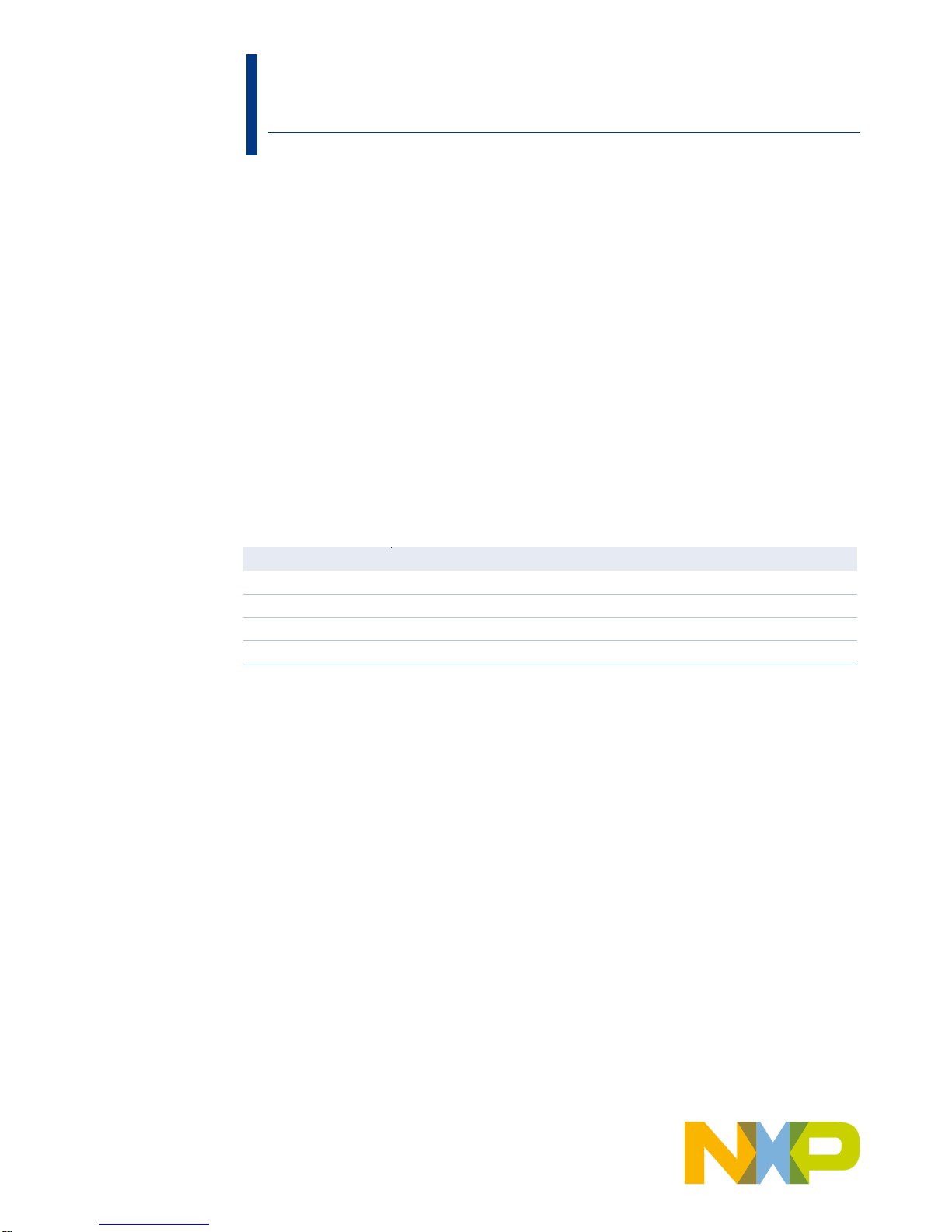
1. Introduction
This document describes the usage of the TJA1100 Customer Evaluation Board. The
Board supports the evaluation of the TJA1100 with providing (MII) a 40-pins standard
header (including MII/SMI/control signals/power supplies. Details can be found in section
2.3.1) with 2,54mm pinning distance to a host controller board, the bus interface (MDI)
including a srew terminal (SMKDS) connector as well as needed components for the
power supply and operation. Further information is given in the following sections.
Please note: the evaluation board has been designed for functional evaluation of the
PHY in your environment. The evaluation board is not intended for EMC or compliance
qualification measurements.
This product has not undergone formal EU EMC assessment. As a component used in a
research environment, it will be the responsibility of the user to ensure the finished
assembly does not cause undue interference when used and cannot be CE marked
unless assessed.
Fig 1. Customer PHY Board Top View
Page 4

NXP Semiconductors
TR1329
Systems & Applications
TR1329
All information provided in this document is subject to legal disclaimers.
© NXP B.V. 2018. All rights reserved.
User Manual
Rev. 01.20 — 31 January 2018
4 of 19
1.1 Acronyms
Table 1. Acronyms used in the document
Acronym
Description
BAT
Battery
DC
Direct Current
GND
Ground
MAC
Medium Access Controller
MDI
Medium Dependent Interface
MII
Medium Independent Interface
PHY
Physical
uC
Microcontroller
Page 5
NXP Semiconductors
TR1329
Systems & Applications
TR1329
All information provided in this document is subject to legal disclaimers.
© NXP B.V. 2018. All rights reserved.
User Manual
Rev. 01.20 — 31 January 2018
5 of 19
2. Board Setup
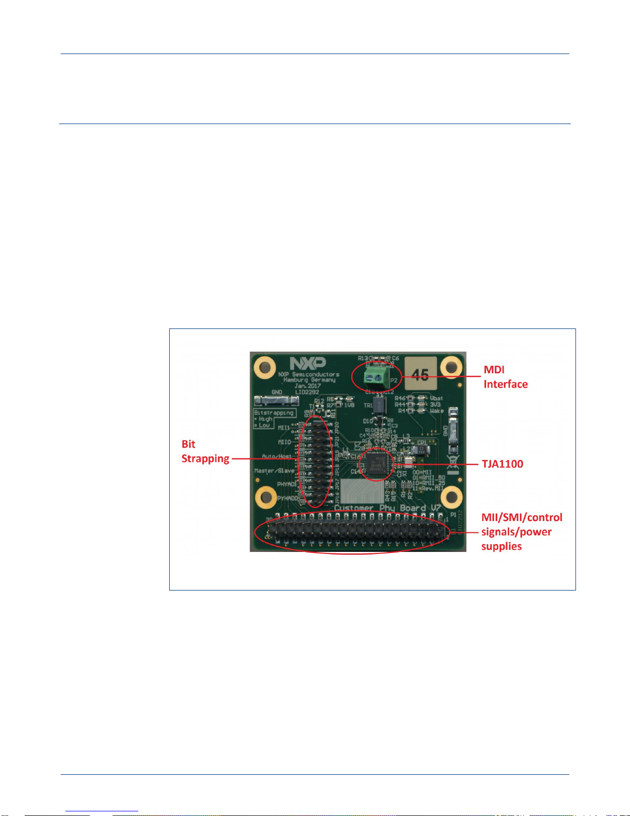
2.1 PHY Assembly
The TJA1100 is provided in a HVQFN-36 package (8x8sqmm). In case the TJA1100 on
the customer evaluation board must be changed, please ensure the correct placement.
The Pin 1 is located at the bottom right and is marked with a small white arrow (see Fig
2).
Fig 2. Pin 1 Location
2.2 Jumper Settings
2.2.1 Bit Strapping
The TJA1100 has several configuration pins for a pre-configuration during startup. The
following tables give an overview of the related jumpers and possible configurations, as
shown also in Fig 3. At the PCB (Fig 4) the orientation for High (H) and Low (L) is
marked.
Please note: all pre-configuration (except for the PHY addresses) can be overwritten via
SMI command.
PHY address is used for the SMI address and for initialization of the Cipher scrambler
key. The PHY address is five bits (PHYAD4…PHYAD0), and PHYAD4 is the MSB of the
address.
PHYAD[4:2] are set to “001” in the TJA1100. PHYAD[1:0] are pre-determined by bit
strapping.
Page 6

NXP Semiconductors
TR1329
Systems & Applications
TR1329
All information provided in this document is subject to legal disclaimers.
© NXP B.V. 2018. All rights reserved.
User Manual
Rev. 01.20 — 31 January 2018
6 of 19
Table 2. Bit Strapping PHY-address
Jumper
Function
Address 4
Address 5
Address 6
Address 7
JP16
Configuration of PHYAD0
L H L
H
JP17
Configuration of PHYAD1
L L H
H
The TJA1100 can be configured as Master or Slave, as well as Managed or Autonomous
operation. When the TJA1100 is configured for Autonomous operation, the PHY will
automatically enter Normal mode and activate the link on power-on without further
interaction with a host controller.
Table 3. Bit Strapping Master/Slave Configuration
Jumper
Function
Master
Slave
JP18
Configuration of CONFIG0
H
L
Table 4. Bit Strapping Managed/autonomous Operation
Jumper
Function
Managed
Autonomous
JP19
Configuration of CONFIG1
L
H
The TJA1100 provides below MII modes, which can be configured via bit strapping.
Table 5. Jumper Settings for Bit Strapping
Jumper
Function
MII
RMII
50MHz
RMII
25MHz
Reverse
MII
JP21
Configuration of CONFIG2
L H L H JP20
Configuration of CONFIG3
L L H
H
Page 7

NXP Semiconductors
TR1329
Systems & Applications
TR1329
All information provided in this document is subject to legal disclaimers.
© NXP B.V. 2018. All rights reserved.
User Manual
Rev. 01.20 — 31 January 2018
7 of 19
Fig 3. Bit Strapping Jumper Settings
Page 8

NXP Semiconductors
TR1329
Systems & Applications
TR1329
All information provided in this document is subject to legal disclaimers.
© NXP B.V. 2018. All rights reserved.
User Manual
Rev. 01.20 — 31 January 2018
8 of 19
Fig 4. Bit Strapping Jumpers on PCB
Page 9

NXP Semiconductors
TR1329
Systems & Applications
TR1329
All information provided in this document is subject to legal disclaimers.
© NXP B.V. 2018. All rights reserved.
User Manual
Rev. 01.20 — 31 January 2018
9 of 19
2.3 Connectors & LEDs
2.3.1 MII Connector
For the MII a double row, 40 pin 2.54x2.54mm male header P1 (Fig 5) is used. At the
PCB (Fig 5Error! Reference source not found.) the pinning order is marked.
The pinning order of the MII connector is given in 0.
Fig 5. MII Connector Location and Pinning Order
Page 10

NXP Semiconductors
TR1329
Systems & Applications
TR1329
All information provided in this document is subject to legal disclaimers.
© NXP B.V. 2018. All rights reserved.
User Manual
Rev. 01.20 — 31 January 2018
10 of 19
Table 6. MII Connector Pinning
Pin Signal
Signal
Pin
1
TJA1100_WAKE
TJA1100_INH
2 3
TJA1100_RSTN
GND
4 5
TJA1100_INT
GND
6 7
TJA1100_MDC
GND
8 9
TJA1100_MDIO
GND
10
11
TJA1100_EN
GND
12
13
TJA1100_TXER
GND
14
15
TJA1100_TXD0
GND
16
17
TJA1100_TXD1
GND
18
19
TJA1100_TXD2
GND
20
21
TJA1100_TXD3
GND
22
23
TJA1100_TXEN
GND
24
25
TJA1100_TXCLK
GND
26
27
TJA1100_RXCLK
GND
28
29
TJA1100_RXD0
GND
30
31
TJA1100_RXD1
GND
32
33
TJA1100_RXD2
GND
34
35
TJA1100_RXD3
3V3
36
37
TJA1100_RXDV
GND
38
39
TJA1100_RXER
BAT
40
Page 11

NXP Semiconductors
TR1329
Systems & Applications
TR1329
All information provided in this document is subject to legal disclaimers.
© NXP B.V. 2018. All rights reserved.
User Manual
Rev. 01.20 — 31 January 2018
11 of 19
2.3.2 MDI Connector
For the MDI interface, a two position PCB terminal connector (SMKDS, 5/2-2.54) from
Phoenix Contact is used, and the details are given in Fig 6.
Fig 6. MDI Pinning Order
Page 12

NXP Semiconductors
TR1329
Systems & Applications
TR1329
All information provided in this document is subject to legal disclaimers.
© NXP B.V. 2018. All rights reserved.
User Manual
Rev. 01.20 — 31 January 2018
12 of 19
2.3.3 LEDs
The LEDs on the Board can be used to evaluate the status of the Board. Fig 7 shows all
the LEDs on the Board, and Table 7 sums up the meaning of each LED.
Fig 7. LEDs on the Board
Table 7. Descriptions of LEDs
LED
Description
LED1
TJA1100 3V3 Power Supply Status (ON: 3V3 is present)
LED2
TJA1100 Local Wake-up Status (Flashing: a Local Wake-up is detected)
LED3
TJA1100 Battery Power Supply Status (ON: Battery is present)
LED4
TJA1100 1V8 Digital Power Supply Status (ON: 1V8 is present)
Page 13

NXP Semiconductors
TR1329
Systems & Applications
TR1329
All information provided in this document is subject to legal disclaimers.
© NXP B.V. 2018. All rights reserved.
User Manual
Rev. 01.20 — 31 January 2018
13 of 19
3. Reference
[1] TJA1100 Datasheet, Version 3, 23 May, 2017
Page 14

NXP Semiconductors
TR1329
Systems & Applications
TR1329
All information provided in this document is subject to legal disclaimers.
© NXP B.V. 2018. All rights reserved.
User Manual
Rev. 01.20 — 31 January 2018
14 of 19
4. Appendix
4.1 The TJA1100 Customer Evaluation Board Schematics
Page 15

NXP Semiconductors
TR1329
Systems & Applications
TR1329
All information provided in this document is subject to legal disclaimers.
© NXP B.V. 2018. All rights reserved.
User Manual
Rev. 01.20 — 31 January 2018
15 of 19
Page 16

NXP Semiconductors
TR1329
Systems & Applications
TR1329
All information provided in this document is subject to legal disclaimers.
© NXP B.V. 2018. All rights reserved.
User Manual
Rev. 01.20 — 31 January 2018
16 of 19
5. Legal information
5.1 Definitions
Draft — The document is a draft version only. The content is still under
internal review and subject to formal approval, which may result in
modifications or additions. NXP Semiconductors does not give any
representations or warranties as to the accuracy or completeness of
information included herein and shall have no liability for the consequences
of use of such information.
5.2 Disclaimers
Limited warranty and liability — Information in this document is believed to
be accurate and reliable. However, NXP Semiconductors does not give any
representations or warranties, expressed or implied, as to the accuracy or
completeness of such information and shall have no liability for the
consequences of use of such information.
In no event shall NXP Semiconductors be liable for any indirect, incidental,
punitive, special or consequential damages (including - without limitation lost profits, lost savings, business interruption, costs related to the removal
or replacement of any products or rework charges) whether or not such
damages are based on tort (including negligence), warranty, breach of
contract or any other legal theory.
Notwithstanding any damages that customer might incur for any reason
whatsoever, NXP Semiconductors’ aggregate and cumulative liability
towards customer for the products described herein shall be limited in
accordance with the Terms and conditions of commercial sale of NXP
Semiconductors.
Right to make changes — NXP Semiconductors reserves the right to make
changes to information published in this document, including without
limitation specifications and product descriptions, at any time and without
notice. This document supersedes and replaces all information supplied prior
to the publication hereof.
Suitability for use — NXP Semiconductors products are not designed,
authorized or warranted to be suitable for use in life support, life-critical or
safety-critical systems or equipment, nor in applications where failure or
malfunction of an NXP Semiconductors product can reasonably be expected
to result in personal injury, death or severe property or environmental
damage. NXP Semiconductors accepts no liability for inclusion and/or use of
NXP Semiconductors products in such equipment or applications and
therefore such inclusion and/or use is at the customer’s own risk.
Applications — Applications that are described herein for any of these
products are for illustrative purposes only. NXP Semiconductors makes no
representation or warranty that such applications will be suitable for the
specified use without further testing or modification.
Customers are responsible for the design and operation of their applications
and products using NXP Semiconductors products, and NXP
Semiconductors accepts no liability for any assistance with applications or
customer product design. It is customer’s sole responsibility to determine
whether the NXP Semiconductors product is suitable and fit for the
customer’s applications and products planned, as well as for the planned
application and use of customer’s third party customer(s). Customers should
provide appropriate design and operating safeguards to minimize the risks
associated with their applications and products.
NXP Semiconductors does not accept any liability related to any default,
damage, costs or problem which is based on any weakness or default in the
customer’s applications or products, or the application or use by customer’s
third party customer(s). Customer is responsible for doing all necessary
testing for the customer’s applications and products using NXP
Semiconductors products in order to avoid a default of the applications and
the products or of the application or use by customer’s third party
customer(s). NXP does not accept any liability in this respect.
Export control — This document as well as the item(s) described herein
may be subject to export control regulations. Export might require a prior
authorization from competent authorities.
5.3 Licenses
Purchase of NXP <xxx> components
<License statement text>
5.4 Patents
Notice is herewith given that the subject device uses one or more of the
following patents and that each of these patents may have corresponding
patents in other jurisdictions.
<Patent ID> — owned by <Company name>
5.5 Trademarks
Notice: All referenced brands, product names, service names and
trademarks are property of their respective owners.
<Name> — is a trademark of NXP B.V.
Page 17

NXP Semiconductors
TR1329
Systems & Applications
TR1329
All information provided in this document is subject to legal disclaimers.
© NXP B.V. 2018. All rights reserved.
User Manual
Rev. 01.20 — 31 January 2018
17 of 19
6. List of figures
Fig 1. Customer PHY Board Top View ........................ 3
Fig 2. Pin 1 Location ................................................... 5
Fig 3. Bit Strapping Jumper Settings ........................... 7
Fig 4. Bit Strapping Jumpers on PCB ......................... 8
Fig 5. MII Connector Location and Pinning Order ....... 9
Fig 6. MDI Pinning Order .......................................... 11
Fig 7. LEDs on the Board .......................................... 12
Page 18

NXP Semiconductors
TR1329
Systems & Applications
TR1329
All information provided in this document is subject to legal disclaimers.
© NXP B.V. 2018. All rights reserved.
User Manual
Rev. 01.20 — 31 January 2018
18 of 19
7. List of tables
Table 1. Acronyms used in the document ....................... 4
Table 2. Bit Strapping PHY-address ............................... 6
Table 3. Bit Strapping Master/Slave Configuration ......... 6
Table 4. Bit Strapping Managed/autonomous Operation 6
Table 5. Jumper Settings for Bit Strapping ..................... 6
Table 6. MII Connector Pinning .................................... 10
Table 7. Descriptions of LEDs ...................................... 12
Page 19

NXP Semiconductors
TR1329
Systems & Applications
Please be aware that important notices concerning this document and the product(s)
described herein, have been included in the section 'Legal information'.
© NXP B.V. 2018. All rights reserved.
For more information, please visit: http://www.nxp.com
For sales office addresses, please send an email to: salesaddresses@nxp.com
Date of release: 31 January 2018
Document identifier: TR1329
8. Contents
1. Introduction ......................................................... 3
1.1 Acronyms ........................................................... 4
2. Board Setup ......................................................... 5
2.1 PHY Assembly ................................................... 5
2.2 Jumper Settings ................................................. 5
2.2.1 Bit Strapping ....................................................... 5
2.3 Connectors & LEDs ............................................ 9
2.3.1 MII Connector ..................................................... 9
2.3.2 MDI Connector ................................................. 11
2.3.3 LEDs ................................................................ 12
3. Reference ........................................................... 13
4. Appendix ............................................................ 14
4.1 The TJA1100 Customer Evaluation Board
Schematics....................................................... 14
5. Legal information .............................................. 16
5.1 Definitions ........................................................ 16
5.2 Disclaimers....................................................... 16
5.3 Licenses ........................................................... 16
5.4 Patents ............................................................. 16
5.5 Trademarks ...................................................... 16
6. List of figures ..................................................... 17
7. List of tables ...................................................... 18
8. Contents ............................................................. 19
 Loading...