

Page 1
TFA9812
BTL stereo Class-D audio amplifier with I2S input
Rev. 02 — 22 January 2009 Preliminary data sheet
1. General description
The TFA9812 is a high-efficiency Bridge Tied Load (BTL) stereo Class-D audio amplifier
with a digital I2S audio input. It is available in a HVQFN48 package with exposed die
paddle. The exposed die paddle technology enhances the thermal and electrical
performances of the device.
The TFA9812 features digital sound processing and audio poweramplification.Itsupports
I2C control mode and Legacy mode. In Legacy mode I2C involvement is not needed
because the key features are controlled by hardware pin connections.
2. Features
2.1 General features
A continuous time output power of 2 × 12W(RL=8Ω,V
an external heat sink. Due to the implementation of a programmable thermal foldback
even for high supply voltages, higher ambient temperatures, and/or lower load
impedances, the device operates without sound interrupting behavior.
TFA9812 is designed in such a way that it starts up easily (no special power-up sequence
required). It features various soft and hard impact protection mechanisms to ensure an
application that is both user friendly and robust.
A modulation technique is applied for the TFA9812, which supports common mode choke
approach (1 common mode choke only per BTL amplifier stage). This minimizes the
number of external components.
n 3.3 V and 8 V to 20 V external power supply
n High efficiency and low power dissipation
n Speaker outputs fully short circuit proof across load, to supply lines and ground
n Pop noise free at power-up/power-down and sample rate switching
n Low power Sleep mode
n Overvoltage and undervoltage protection on the 8 V to 20 V power supply
n Undervoltage protection on the 3.3 V power supply
n Overcurrent protection (no audible interruptions)
n Overdissipation protection
n Thermally protected and programmable thermal foldback
n Clock error protection
n I2C mode control or Legacy mode (i.e. no I2C) control
n Four different I2C addresses supported
n Internal Phase-Locked Loop (PLL) without using external components
= 15 V) is supported without
DDP
Page 2

NXP Semiconductors
n No high system clock required (PLL is able to lock on BCK)
n No external heat sink required
n 5 V tolerant digital inputs
n Supports dual coil inductor application
n Easy application and limited external components required
2.2 DSP features
n Digital parametric 10-band equalizer
n Digital volume control per channel
n Selectable +24 dB gain boost
n Analog interface to digital volume control in Legacy mode
n Digital clip level control
n Soft and hard mute
n Thermal foldback threshold temperature control
n De-emphasis
n Output power limiting control
n Polarity switch
n Four Pulse Width Modulation (PWM) switching frequency settings
TFA9812
BTL stereo Class-D audio amplifier with I2S input
2.3 Audio data input interface format support
n Master or slave Master Clock (MCLK), Bit Clock (BCK) and Word Select (WS) signals
n Philips I2S, standard I2S
n Japanese I2S, Most Significant Bit (MSB) justified
n Sony I2S, Least Significant Bit (LSB) justified
n Sample rates from 8 kHz to 192 kHz
3. Applications
n Digital-in Class-D audio amplifier applications
n CRT and flat-panel television sets
n Flat-panel monitors
n Multimedia systems
n Wireless speakers
n Docking stations for MP3 players
TFA9812_2 © NXP B.V. 2009. All rights reserved.
Preliminary data sheet Rev. 02 — 22 January 2009 2 of 66
Page 3

NXP Semiconductors
4. Quick reference data
Table 1. Quick reference table
Unless specified otherwise, V
V
SS1=VSS2
24-bit I
Symbol Parameter Conditions Min Typ Max Unit
General
V
DDA
V
DDP
V
DDA(3V3)
V
DDD(3V3)
I
P
I
DDA(3V3)
I
DDD(3V3)
P
o(RMS)
η
po
= REFD = REFA = 0 V, T
2
S input data, MCLK clock mode, typical application diagram (Figure 13).
TFA9812
BTL stereo Class-D audio amplifier with I2S input
DDA=VDDP
=12V,V
=25°C, RL=8Ω,fi= 1 kHz, fs= 44.1 kHz, fsw= 400 kHz,
amb
SSP1=VSSP2
analog supply
voltage
power supply
voltage
analog supply
voltage (3.3 V)
digital supply
voltage (3.3 V)
supply current soft mute mode, withload,
filter and snubbers
connected
sleep mode
analog supply
current (3.3 V)
operating mode
2
S slave mode - 2 4 mA
I
2
S master mode - 4 6 mA
I
sleep mode
= 12 V - 120 - µA
= 1 V - 40 70 µA
digital supply
current (3.3 V)
V
DDA=VDDP
V
DDA=VDDP
operating mode
2
S slave mode - 15 25 mA
I
2
S master mode - 25 40 mA
I
sleep mode;
DATA = WS = BCK =
MCLK = 0 V
RMS output power Continuous time output power per channel; THD = 10 %;
R
=8Ω
L
= V
V
DDA
= V
V
DDA
= V
V
DDA
= 12 V - 8.3 - W
DDP
= 13.5 V - 10 - W
DDP
= 15 V - 12 - W
DDP
Short time (≤ 10 s) output power per channel; THD = 10 %;
=8Ω
R
L
output power
= V
V
DDA
RL=8Ω; P
= 17 V - 15 - W
DDP
= 8.3 W - 88 - %
o(RMS)
efficiency
=0V,V
DDA(3V3)=VDDD(3V3)
81220V
81220V
3.0 3.3 3.6 V
3.0 3.3 3.6 V
[1]
-3845mA
[1]
- 160 270 µA
-430µA
= 3.3 V,
[1] IPis thecurrent through theanalog supply voltage(V
voltage (V
TFA9812_2 © NXP B.V. 2009. All rights reserved.
Preliminary data sheet Rev. 02 — 22 January 2009 3 of 66
DDP
) pin.
) pin added to the current through the power supply
DDA
Page 4

NXP Semiconductors
BTL stereo Class-D audio amplifier with I2S input
5. Ordering information
Table 2. Ordering information
Type number Package
Name Description Version
TFA9812HN HVQFN48 plastic thermal enhanced very thin quad flat package; no leads;
48 terminals; body 7 × 7 × 0.85 mm
TFA9812
SOT619-8
TFA9812_2 © NXP B.V. 2009. All rights reserved.
Preliminary data sheet Rev. 02 — 22 January 2009 4 of 66
Page 5
xxxxxxxxxxxxxxxxxxxxx xxxxxxxxxxxxxxxxxxxxxxxxxx xxxxxxx x x x xxxxxxxxxxxxxxxxxxxxxxxxxxxxxx xxxxxxxxxxxxxxxxxxx xx xx
xxxxx xxxxxxxxxxxxxxxxxxxxxxxxxxx xxxxxxxxxxxxxxxxxxx xxxxxx xxxxxxxxxxxxxxxxxxxxxxxxxxxxxxxxxxx xxxxxxxxxxxx x x
xxxxxxxxxxxxxxxxxxxxx xxxxxxxxxxxxxxxxxxxxxxxxxxxxxx xxxxx xxxxxxxxxxxxxxxxxxxxxxxxxxxxxxxxxxxxxxxxxxxxxxxxxx xxxxxxxx
TFA9812_2 © NXP B.V. 2009. All rights reserved.
Preliminary data sheet Rev. 02 — 22 January 2009 5 of 66
xxxxxxxxxxxxxxxxxxxxxxxxx xxxxxxxxxxxxxxxxxxxx xxx
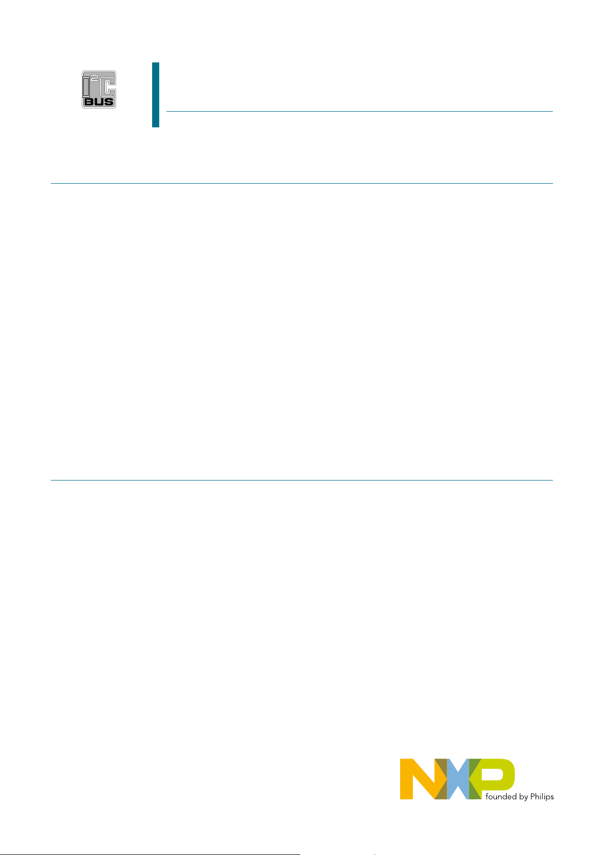
6. Block diagram
NXP Semiconductors
TEST1 TEST2 AVOL V
743 32 40 36
PHASED
LOCKED
LOOP
XTALIN
1
OSCILLATOR
MCLK
BCK
WS
DATA
GAIN
CSEL
SDA/MS
2
47
46
45
44
INTERFACE
31
33ENABLE
34
35
36
37
38
39
SERIAL
AUDIO
CONTROL
INTERFACE
PARAMETRIC
EQUALIZER
XTALOUT
POWERUP
ADSEL2/PLIM2
ADSEL1/PLIM1
SCL/SFOR
Fig 1. TFA9812 block diagram
CLOCK
PROTECTION
LP
UFP
OFP
IBP
10-BAND
PROTECTION
OVP
UVP
OCP
OTP
ODP
WP
REGISTER
ADDRESS
HEX 01
VOLUME
CONTROL
AND SOFT
MUTE
29
10
CDELAYDIAG
DDD(3V3)VDDA(3V3)VDDA
ADC
CSEL
THERMAL
FOLDBACK
INTER-
POLATION
FILTER AND
DE-EMPHASIS
41
30
STABD REFD STABA REFA
GAIN
REFERENCES
42
TFA9812
POWER
LIMITER
45
PWM
CONTROLLER
PWM
CONTROLLER
EXPOSED DIE PADDLE V
CONTROL
LOGIC
CONTROL
LOGIC
CONTROL
LOGIC
CONTROL
LOGIC
DRIVER
HIGH
DRIVER
LOW
DRIVER
HIGH
DRIVER
LOW
DRIVER
HIGH
DRIVER
LOW
DRIVER
HIGH
DRIVER
LOW
SS1VSS2
STAB1
STAB2
488
18, 19
16, 17
10, 11
V
DDP
23, 24
26, 27
V
DDP
20, 21
V
SSP2
V
DDP
13, 14
V
SSP2
15
25
28
22
12
9
BOOT1P
V
DDP
OUT1P
V
SSP2
BOOT1N
OUT1N
V
SSP1
STAB1
BOOT2P
OUT2P
BOOT2N
OUT2N
STAB2
010aaa217
BTL stereo Class-D audio amplifier with I
TFA9812
2
S input
Page 6

NXP Semiconductors
Figure 1 shows the block diagram of the TFA9812. For a detailed description of the audio
signal path see Section 8.1.
7. Pinning information
7.1 Pinning
TFA9812
BTL stereo Class-D audio amplifier with I2S input
terminal 1
index area
XTALIN ADSEL2/PLIM2
XTALOUT CSEL
V
DDA(3V3)
STABA ENABLE
REFA AVOL
V
DDA
TEST1 CDELAY
V
SS1
STAB2 STAB1
V
SSP2
V
SSP2
BOOT2N
SS2
V
MCLK
BCKWSDATA
4847464544434241403938
1 36
2 35
3 34
4 33
5 32
6 31
7 30
8 29
9 28
10 27
11 26
12 25
1314151617181920212223
OUT2N
OUT2N
BOOT1P
TEST2
TFA9812HN
DDPVDDP
V
OUT2P
OUT1P
Transparent top view
REFD
DDD(3V3)
STABD
V
OUT1P
OUT1P
SDA/MS
SCL/SFOR
OUT1N
BOOT1P
ADSEL1/PLIM1
37
24
OUT1N
GAIN
POWERUP
DIAG
V
SSP1
V
SSP1
BOOT1N
010aaa218
Fig 2. Pin configuration, transparent top view
Table 3. Pinning description TFA9812
Pin Symbol Type Description
1 XTALIN I Crystal oscillator input
2 XTALOUT O Crystal oscillator output
3V
DDA(3V3)
P Analog supply voltage (3.3 V)
4 STABA O 1.8 V analog stabilizer output
5 REFA P Analog reference voltage
6V
DDA
P Analog supply voltage (8 V to 20 V)
7 TEST1 I Test signal input 1. For test purposes only (connect to V
8V
SS1
P PCB ground reference
9 STAB2 O Decoupling of internal 11 V regulator for channel 2 drivers
10 V
11 V
SSP2
SSP2
P Negative power supply voltage for channel 1 and channel 2
P Negative power supply voltage for channel 1 and channel 2
12 BOOT2N O Bootstrap high-side driver negative PWM output channel 2
13 OUT2N O Negative PWM output channel 2
SS
)
TFA9812_2 © NXP B.V. 2009. All rights reserved.
Preliminary data sheet Rev. 02 — 22 January 2009 6 of 66
Page 7

NXP Semiconductors
TFA9812
BTL stereo Class-D audio amplifier with I2S input
Table 3. Pinning description TFA9812
…continued
Pin Symbol Type Description
14 OUT2N O Negative PWM output channel 2
15 BOOT1P O Bootstrap high-side driver positive PWM output channel 1
16 OUT1P O Positive PWM output channel 1
17 OUT1P O Positive PWM output channel 1
18 V
19 V
DDP
DDP
P Positive power supply voltage (8 V to 20 V)
P Positive power supply voltage (8 V to 20 V)
20 OUT2P O Positive PWM output channel 2
21 OUT2P O Positive PWM output channel 2
22 BOOT2P O Bootstrap high-side driver positive PWM output channel 2
23 OUT1N O Negative PWM output channel 1
24 OUT1N O Negative PWM output channel 1
25 BOOT1N O Bootstrap high-side driver negative PWM output channel 1
26 V
27 V
SSP1
SSP1
P Negative power supply voltage for channel 1 and channel 2
P Negative power supply voltage for channel 1 and channel 2
28 STAB1 O Decoupling of internal 11 V regulator for channel 1 drivers
29 DIAG O Fault mode indication output (open-drain pin)
30 CDELAY I Timing reference
31 POWERUP I Power-up pin to switch betweenSleep and other operational
modes
32 AVOL I Analog volume control (Legacy mode)
33 ENABLE I Enable input to switch between 3-state and other
operational modes
34 GAIN I Gain selection input to select between 0 dB and +24 dB
gain (Legacy mode)
35 CSEL I Control selection input to select between Legacy mode
2
C bus control) and I2C bus control
(no I
2
36 ADSEL2/PLIM2 I Address selection in I
C mode input 2, power limiter
selection input 2 in Legacy mode
2
37 ADSEL1/PLIM1 I Address selection in I
C mode input 1, power limiter
selection input 1 in Legacy mode
2
38 SCL/SFOR I I
C bus clock input in I2C mode, I2S serial data format
selection input in Legacy mode
2
39 SDA/MS I/O I
C bus data input and output in I2C mode, master/slave
selection input in Legacy mode
40 V
DDD(3V3)
P Digital supply voltage (3.3 V)
41 STABD O 1.8 V digital stabilizer output
42 REFD P Digital reference voltage
43 TEST2 I Test signal input 2; for test purposes only (connect to V
2
44 DATA I I
45 WS I/O I
S bus data input
2
S bus word select input (I2S slave mode) or output (I2S
SS
master mode)
2
46 BCK I/O I
S bus bit clock input (I2S slave mode) or output (I2S
master mode)
)
TFA9812_2 © NXP B.V. 2009. All rights reserved.
Preliminary data sheet Rev. 02 — 22 January 2009 7 of 66
Page 8

NXP Semiconductors
TFA9812
BTL stereo Class-D audio amplifier with I2S input
Table 3. Pinning description TFA9812
Pin Symbol Type Description
47 MCLK I/O Master clock input (I2S slave mode) or output (I2S master
48 V
Exposed
die-paddle
SS2
- P PCB ground reference
8. Functional description
8.1 General
The TFA9812 is a high-efficiency stereo BTL Class-D amplifier with a digital I2S audio
input. It supports all commonly used I2S formats.
Figure 1 shows the functional block diagram, which includes the key function blocks of the
TFA9812. In the digital domain the audio signal is processed and converted to a pulse
width modulated signal using BD modulation. A BTL configured power comparator carries
out power amplification.
The audio signal processing path is as follows:
1. The Digital Audio Input (DAI) block translates the I2S (-like) input signal into a
standard internal stereo audio stream.
2. The 10-band parametric equalizer can optionally equalize the stereo audio stream.
Both channels have separate equalization streams. It can be used forspeaker transfer
curve compensation to optimize the audio performance of applied speakers.
3. Volume control in the TFA9812 is done by attenuation. The attenuation depends on
the volume control settings and the thermal foldbackvalue. Soft mute is also arranged
at this part. In Legacy mode the volume control is done by an on-board
Analog-to-Digital Converter (ADC) which measures the analog voltage on pin 32.
4. The interpolation filter interpolates from 1 fs to the PWM controller sample rate
(2048 fs at 44.1 kHz) by cascading FIR filters.
5. The gain block can boost the signal with 0 dB or +24 dB. Four specific gain settings
are also provided in this block. These specific gain settings are related to maximum
clip levels of < 0.5 %, 10 %, 20 % or 30 % THD at the TFA9812 output. These
maximum clip levels are only valid with the gain boost set to 0 dB and a 0 dBFS input
signal.
6. The power limiter limits the maximum output signal of the TFA9812. The power limiter
settings are 0 dB, −1.5 dB, −3 dB, and −4.5 dB. This function can be used to reduce
the maximum output power delivered to the speakers at a fixed supply voltage and
speaker impedance.
7. The PWM controller block transforms the audio signal into a BD-modulated PWM
signal. The BD-modulation provides a high signal-to-noise performance and
eliminates clock jitter noise.
8. Via four differential comparators the PWM signals are amplified by two BTL power
output stages. By default the left audio signal is connected to channel 1 and the right
audio signal to channel 2.
…continued
mode)
P PCB ground reference
TFA9812_2 © NXP B.V. 2009. All rights reserved.
Preliminary data sheet Rev. 02 — 22 January 2009 8 of 66
Page 9

NXP Semiconductors
The block control defines the operational control settings of the TFA9812 in line with the
actual I2C settings and the pin-controlled settings.
The PLL block creates the system clock and can take the I2S BCK, the MCLK or an
external crystal as reference source.
The following protections are built into the TFA9812:
• Thermal Foldback (TF)
• OverTemperature Protection (OTP)
• OverCurrent Protection (OCP)
• OverVoltage Protection (OVP)
• UnderVoltage Protection (UVP)
• Window Protection (WP)
• Lock Protection (LP)
• UnderFrequency Protection (UFP)
• OverFrequency Protection (OFP)
• Invalid BCK Protection (IBP)
• DC-blocking
• ElectroStatic Discharge (ESD)
TFA9812
BTL stereo Class-D audio amplifier with I2S input
8.2 Functional modes
8.2.1 Control modes
The two control modes of the TFA9812 are I2C and legacy.
2
• In I
C mode the I2C format control is enabled.
• In Legacy mode a pin-based subset of the control options is available. The control
settings for features which are not available in Legacy mode are set to the default I2C
register settings.
The control mode is selected via pin CSEL as shown in Table 4.
Table 4. Control mode selection
CSEL Pin value Control mode
0 Legacy (no I
2
1I
In the functional descriptions below the control for the various functions will be described
for each control mode. Section 9.6 summarizes the support given by each control mode
for the various TFA9812 functions.
8.2.2 Key operating modes
There are six key operating modes:
C
2
C)
• InSleep mode the voltage supplies are present, but power consumption for the whole
device is reduced to the minimum level. The output stages in Sleep mode are 3-state
and I2C communication is disabled.
TFA9812_2 © NXP B.V. 2009. All rights reserved.
Preliminary data sheet Rev. 02 — 22 January 2009 9 of 66
Page 10

NXP Semiconductors
TFA9812
BTL stereo Class-D audio amplifier with I2S input
• In Soft mute mode the I
2
S input signal is overruled with a soft mute.
– In Legacy control mode the analog input pin AVOL controls Soft mute mode.
– In I2C control mode I2C control can be used to enable an automatic soft mute
function. See also Section 8.5.3.
• In Hard mute mode the PWM controller is overruled with a 50 % duty cycle square
pulse. The Hard mute mode is only available in I2C control mode.
• In Operating mode the TFA9812 amplifies the I
2
S audio input signal in line with the
actual control setting.
• In 3-state mode the output stages are switched off.
• Fault mode is entered when a fault condition is detected by one or more of the
protection mechanisms implemented in the TFA9812. In Fault mode the actual device
configuration depends on the fault detected: see Section 8.7 for more information.
Fault mode is for a subset of the faults flagged on the DIAG output pin. When the
DIAG pin is flagged the output stages will be forced to enter 3-state mode. In Sleep
mode the DIAG pin will not flag fault modes.
Table 5. Operational mode selection
Pin: DIAG Output Operational mode
selected:
POWERUP ENABLE CSEL AVOL
0 - - - floating Sleep mode
1 - - - 0 / floating Fault mode (enabled by
system)
1 1 1 - floating Soft mute mode (in I2C
control mode)
1 1 0 < 0.8 V floating Soft mute (in Legacy control
mode)
1 0 - - floating 3-state mode
1 1 - - floating Operational mode
[1]
[2]
[1] Clocking faults do not trigger DIAG output.
[2] Under these conditions soft mute still has to be enabled by the appropriate I2C setting.
8.2.3 I2S master/slave modes and MCLK/BCK clock modes
The I2S interface can be set in master or in slave.
2
• In I
S master mode the PLL locks to the output signal of the internal crystal oscillator
circuit which uses an external crystal. The BCK, WS and MCLK signals are generated
by the TFA9812. On the MCLK pin the TFA9812 delivers a master clock running at the
crystal frequency.
2
• In I
S slave mode the PLL can lock to:
– The external MCLK signal on the MCLK pin called MCLK clock mode.
– The I2S input BCK signal on the BCK pin called BCK clock mode.
The I2S master or slave mode can be selected:
2
• In I
C control mode by selecting the right I2C setting.
• In legacy control mode by selecting the right setting on the SDA/MS pin.
TFA9812_2 © NXP B.V. 2009. All rights reserved.
Preliminary data sheet Rev. 02 — 22 January 2009 10 of 66
Page 11

NXP Semiconductors
Table 6. I2S master/slave mode selection
Pin value Clock mode I2S mode
CSEL SDA/MS
0 0 legacy slave
0 1 legacy master
1- I
[1] Under these conditions the mode is enabled by the appropriate I2C setting.
In I2S slave mode selection between BCK and MCLK clock modes is automatic.
MCLK clock mode is given higher priority than BCK. If the MCLK clock is judged valid by
the protection circuit then MCLK clock mode is enabled. BCK clock mode is enabled when
the MCLK clock is invalid (e.g. not available) and the BCK clock is judged valid by the
protection circuit (see Section 8.7.11).
Table 7 shows the supported crystal frequencies in I2S master mode.
Table 8 shows the supported MCLK frequencies in MCLK mode (I2S slave mode).
TFA9812
BTL stereo Class-D audio amplifier with I2S input
2
C slave or master
[1]
Table 9 shows the supported BCK frequencies in BCK mode (I2S slave mode).
Table 7. Valid crystal frequencies in I2S master mode
Control mode fs (kHz) Crystal frequency (MHz)
2
C 8, 16, 32, 64, 128 8.192
I
11.025, 22.05, 44.1, 88.2,
176.4
12, 24, 48, 96, 192 12.288
Legacy 32 8.192
44.1 11.2896
48 12.288
2
Table 8. Valid MCLK frequencies in I
S slave mode
Control mode fs (kHz) MLCK frequency (MHz)
2
C 8, 16, 32, 64, 128 8.192
I
32 18.432 (576 f
11.025, 22.05, 44.1, 88.2,
176.4
44.1 25.4016 (576 f
12, 24, 48, 96, 192 12.288
48 27.648 (576 f
11.2896
12.288
11.2896
16.9344
18.432
)
s
)
s
)
s
TFA9812_2 © NXP B.V. 2009. All rights reserved.
Preliminary data sheet Rev. 02 — 22 January 2009 11 of 66
Page 12

NXP Semiconductors
Table 8. Valid MCLK frequencies in I2S slave mode
Control mode fs (kHz) MLCK frequency (MHz)
Legacy 32 8.192
TFA9812
BTL stereo Class-D audio amplifier with I2S input
12.288
18.432 (576 f
44.1 11.2896
16.9344
25.4016 (576 f
48 12.288
18.432
27.648 (576 f
)
s
)
s
)
s
Table 9. Valid BCK frequencies in I
2
S slave mode
Control mode fs (kHz) BCK (x fs input)
2
C 8 to 192
I
8 to 192
8 to 192
Legacy 32, 44.1, 48 32 f
32, 44.1, 48 48 f
32, 44.1, 48 64 f
[1] The valid sample frequencies are shown in Section 9.5.7.
[1]
[1]
[1]
32 f
48 f
64 f
s
s
s
s
s
s
TFA9812_2 © NXP B.V. 2009. All rights reserved.
Preliminary data sheet Rev. 02 — 22 January 2009 12 of 66
Page 13
NXP Semiconductors
8.3 Power-up/power-down
external
voltage
supplies
POWERUP
pin
ENABLE
pin
2
I
available
soft mute
setting in
2
C mode
I
AVOL pin
in Legacy
mode
TFA9812
BTL stereo Class-D audio amplifier with I2S input
C
PWM
outputs
Operating
mode active
Fig 3. Power-up/power-down timing
8.3.1 Power-up
Figure 3 and Table 10 describe the power-up timing while Table 11 shows the pin control
for initiating a power-up reset.
Table 10. Power-up/power-down timing
Symbol Parameter Conditions Min Typ Max Unit
t
wake
t
d(on)
t
d(mute_off)
t
d(soft_mute)
wake-up
time
turn-on
delay time
mute off
delay time
Soft mute
delay time
t
wake
t
d(on)
t
d(mute_off)
t
d(soft_mute)
I2C control - 4 - ms
- 70 - 135 ms
- - - 128/f
I2C control - - 128/f
legacy
control
-15-ms
[1]
s
s
010aaa219
s
s
[1] Mute in Legacy mode is controlled by AVOL pin.
TFA9812_2 © NXP B.V. 2009. All rights reserved.
Preliminary data sheet Rev. 02 — 22 January 2009 13 of 66
Page 14

NXP Semiconductors
In I2C control mode communication is enabled after 4 ms. The preferred I2C settings can
be made within 66 ms before the PLL starts running. Finally, the output stages are
enabled and the audio level is increased via a demute sequence if mute has previously
been disabled.
Remark: In I2C mode soft mute is enabled by default. It can be disabled at any time while
I2C communication is valid. In order to prevent audio clicks volume control (default setting
is 0 dB) should be set before soft mute is disabled.
Remark: For a proper start-up in I2S master mode and I2C mode the following sequence
should be followed:
1. The I2S master setting should be set and keep the default sample rate setting active.
2. Next, another sample rate setting than the default one should be selected.
3. Finally, when the default sample rate is used the default sample rate setting should be
8.3.2 Power-down
Figure 3 includes the power-down timing while Table 11 shows the pin control for enabling
power-down.
TFA9812
BTL stereo Class-D audio amplifier with I2S input
selected again.
Table 11. Power-up/power-down selection
Power-up pin
value
0 Power-down (Sleep mode)
1 Power-up
Description
Putting the TFA9812 into power-down is equivalent to enabling Sleep mode
(see Section 8.2.2). This mode is entered immediately and no additional clock cycles are
required.
In order to prevent audible clicks, soft mute should be enabled at least T
d(soft_mute)
seconds before enabling Sleep mode.
The specified low current and power conditions in Table 1 are valid within 10 µs after
enabling Sleep mode.
8.4 Digital audio data input
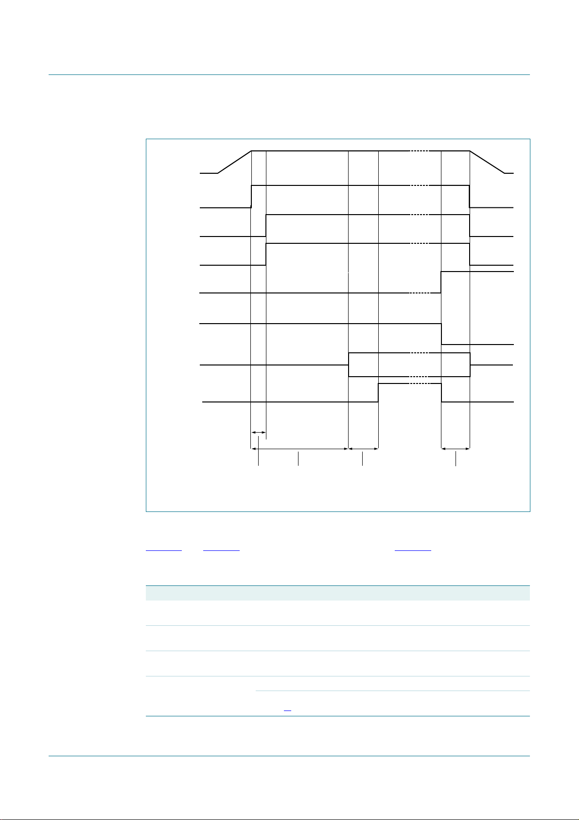
8.4.1 Digital audio data format support
The TFA9812 supports a commonly used range of I2S and I2S-like digital audio data input
formats. These are listed in Table 12.
Table 12. Supported digital audio data formats
BCK frequency Interface format (MSB first) Supported in I2C
control mode
32 f
s
32 f
s
32 f
s
48 f
s
48 f
s
TFA9812_2 © NXP B.V. 2009. All rights reserved.
Preliminary data sheet Rev. 02 — 22 January 2009 14 of 66
I2S up to 16-bit data yes yes
MSB-justified 16-bit data yes yes
LSB-justified 16-bit data yes yes
I2S up to 24-bit data yes yes
MSB-justified up to 24-bit data yes yes
Supported in Legacy
control mode
Page 15
NXP Semiconductors
Table 12. Supported digital audio data formats
BCK frequency Interface format (MSB first) Supported in I2C
48 f
48 f
48 f
48 f
64 f
64 f
64 f
64 f
64 f
64 f
Remark: Only MSB-first formats are supported.
TFA9812
BTL stereo Class-D audio amplifier with I2S input
Supported in Legacy
control mode
s
s
s
s
s
s
s
s
s
s
LSB-justified 16-bit data yes no
LSB-justified 18-bit data yes no
LSB-justified 20-bit data yes no
LSB-justified 24-bit data yes yes
I2S up to 24-bit data yes yes
MSB-justified up to 24-bit data yes yes
LSB-justified 16-bit data yes no
LSB-justified 18-bit data yes no
LSB-justified 20-bit data yes no
LSB-justified 24-bit data yes no
control mode
LEFT
LEFT
2
I
MSB-JUSTIFIED FORMAT
LEFT
LEFT
LEFT
MSB B2 B3 B4 B5 B6
LEFT
WS
BCK
DATA
WS
BCK
DATA
WS
BCK
DATA
WS
BCK
DATA
WS
BCK
DATA
WS
BCK
MSB B2
MSB B2 MSBLSB LSB MSB B2B2
2112 3
MSB MSBB2
S-BUS FORMAT
MSB B2 B3 B4
RIGHT
3
RIGHT
321321
16
15 2 1
MSB
B2
1518 17 2 1
16
1518 1720 19 2 1
16
1518 1720 1922 212324 2 1
16
B15
LSB
LSB-JUSTIFIED FORMAT 16 BITS
B17
LSB
LSB-JUSTIFIED FORMAT 18 BITS
B19
LSB
LSB-JUSTIFIED FORMAT 20 BITS
RIGHT
16
MSB B2
RIGHT
16 1518 17 2 1
MSB B2 B3 B4
RIGHT
16
MSB B2 B3 B4 B5 B6
RIGHT
16
15 2 1
B15 LSB
B17 LSB
1518 1720 19 2 1
B19 LSB
1518 1720 1922 212324 2 1
DATA
MSB
B5 B6 B7 B8 B9 B10
B3 B4
B2
B23
LSB
LSB-JUSTIFIED FORMAT 24 BITS
MSB
B5 B6 B7 B8 B9 B10
B3 B4
B2
B23 LSB
010aaa458
Fig 4. Serial interface input and output formats
TFA9812_2 © NXP B.V. 2009. All rights reserved.
Preliminary data sheet Rev. 02 — 22 January 2009 15 of 66
Page 16

NXP Semiconductors
In I2C control mode the following sample frequency fs can be used: 8 kHz, 11.025 kHz,
12 kHz, 16 kHz, 22.05 kHz, 24 kHz, 32 kHz, 44.1 kHz, 48 kHz, 64 kHz, 88.2 kHz, 96 kHz,
128 kHz, 176.4 kHz or 192 kHz. The I2C control for fs selection can be found in
Section 9.5.7.
In Legacy control mode the following sample frequencies (fs) can be used: 32 kHz,
44.1 kHz or 48 kHz.
8.4.2 Digital audio data format control
The BCK-to-WS and MCLK-to-WS frequency ratios are automatically detected, so no
control settings need to be configured for these.
In I2C control mode all the formats listed in Table 12 are supported. The appropriate I2C
controls for selecting the supported formats can be found in Section 9. In the Legacy
control mode only a subset of the supported formats can be used. These are shown in
Table 12 and the required pin control is given in Table 13.
See Section 8.2.1 for details of how to enable Legacy control mode.
Table 13. Digital audio data format selection in Legacy control mode
SCL/SFOR pin value Interface formats (MSB-first)
0I
1 MSB-justified
TFA9812
BTL stereo Class-D audio amplifier with I2S input
2
S
8.5 Digital signal-processing features
8.5.1 Equalizer
8.5.1.1 Equalizer options
The equalizer function can be bypassed and the equalizer can be configured to either a
5-band or 10-band function. These settings are for both audio channels simultaneously.
There are 20 bands in the equalizer. These are distributed as follows:
• Bands A1 to A5 are bands 1 to 5 of output 1 (used in 5-band and 10-band
configuration).
• Bands B1 to B5 are bands 1 to 5 of output 2 (used in 5-band and 10-band
configuration).
• Bands C1 to C5 are bands 6 to 10 of output 1 (used in 10-band configuration only).
• Bands D1 to D5 are bands 6 to 10 of output 2 (used in 10-band configuration only).
In I2C control mode each band can be configured separately using I2C register settings.
In Legacy control mode the equalizer is bypassed.
8.5.1.2 Equalizer band function
The shape of each parametric equalizer band is determined by the three filter parameters:
• (Relative) center frequency .
ω 2π fcfs⁄()=
• Quality factor Q.
• Gain factor G.
TFA9812_2 © NXP B.V. 2009. All rights reserved.
Preliminary data sheet Rev. 02 — 22 January 2009 16 of 66
Page 17
NXP Semiconductors
In the above equation fcis the center frequency and fs is the sample frequency.
The definition of the quality factor is the center frequency divided by the 3 dB bandwidth,
see Equation 1. In parametric equalizers this is only valid when the gain is set very small
(−30 dB).
Q
Each band filter can be programmed to perform a band-suppression (G < 1) or a
band-amplification (G > 1) function around the center frequency.
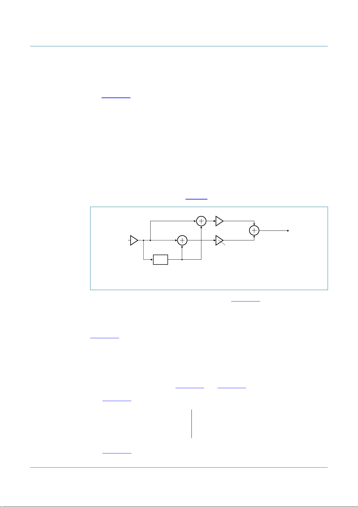
Each band of the TFA9812 equalizer has a second-order Regalia-Mitra all-pass filter
structure. The structure is shown in Figure 5.
f
c
-----------------
f2f1–
;=
f1: 20
f2: 20
BTL stereo Class-D audio amplifier with I2S input
A
10
10
f
1
log 3dB fcf1>=
--------
A
f
c
A
f
2
log 3dB f2fc>,=
--------
A
f
c
TFA9812
(1)
s
X(z)
A(z)
Fig 5. Regalia filter flow-diagram
+
+
−
½
+
K0/2
Y(z)
010aaa406
The transfer function of this all-pass filter is shown in Equation 2:
Hz() 12⁄ 1Az()+()K02⁄ 1Az()–()⋅+⋅=
A(z) is the second-order filter structure. The transfer function of A(z) is shown in
Equation 3:
Az()
K1K21K
=
-------------------------------------------------------------------------------- -
1K21K
+()Z1–Z2–+⋅⋅+
1
+()Z1–K1Z2–⋅+⋅⋅+
1
The relationship between the programmable parameters K0, K1, and K2 and the filter
parameters G, ω, Q is shown in Equation 4 and Equation 5.
(2)
(3)
Use Equation 4 to calculate band suppression (G < 1) functions.
K
G=
0
K
1
K
2Q G ωsin–⋅()2Q G ωsin+⋅()⁄=
2
ωcos–=
G1<
(4)
Use Equation 5 to calculate band amplification (G ≥ 1) functions.
TFA9812_2 © NXP B.V. 2009. All rights reserved.
Preliminary data sheet Rev. 02 — 22 January 2009 17 of 66
Page 18

NXP Semiconductors
TFA9812
BTL stereo Class-D audio amplifier with I2S input
K0G=
K
1
K
2Q ωsin–()2Q ωsin+()⁄=
2
ωcos–=
G1≥
The ranges of the TFA9812 parametric equalizer settings for each band are:
• The Gain, G is from −30 dB to +12 dB.
• The center frequency, f
is from 0.0004 * fs to 0.49 * fs.
c
• The quality factor Q is from 0.001 to 8.
Using I2C control, filter coefficients need to be entered for each filter stage to configure it
as desired.
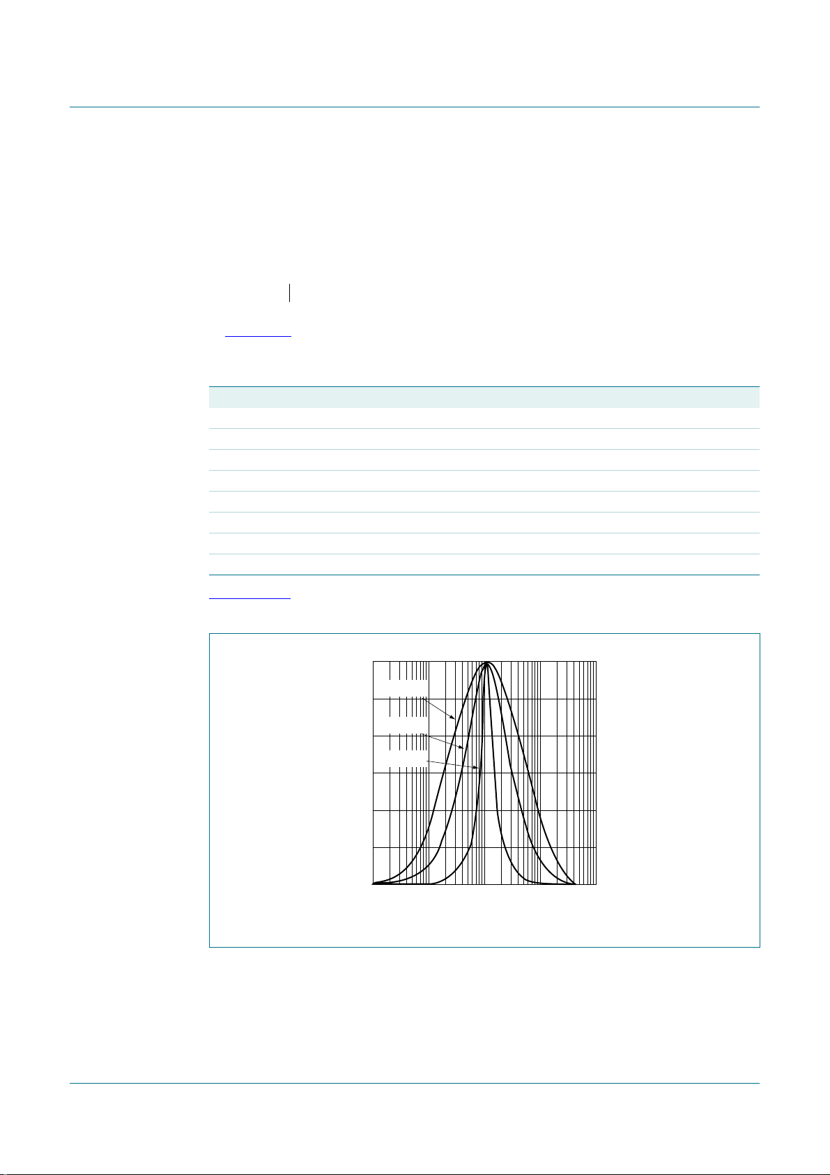
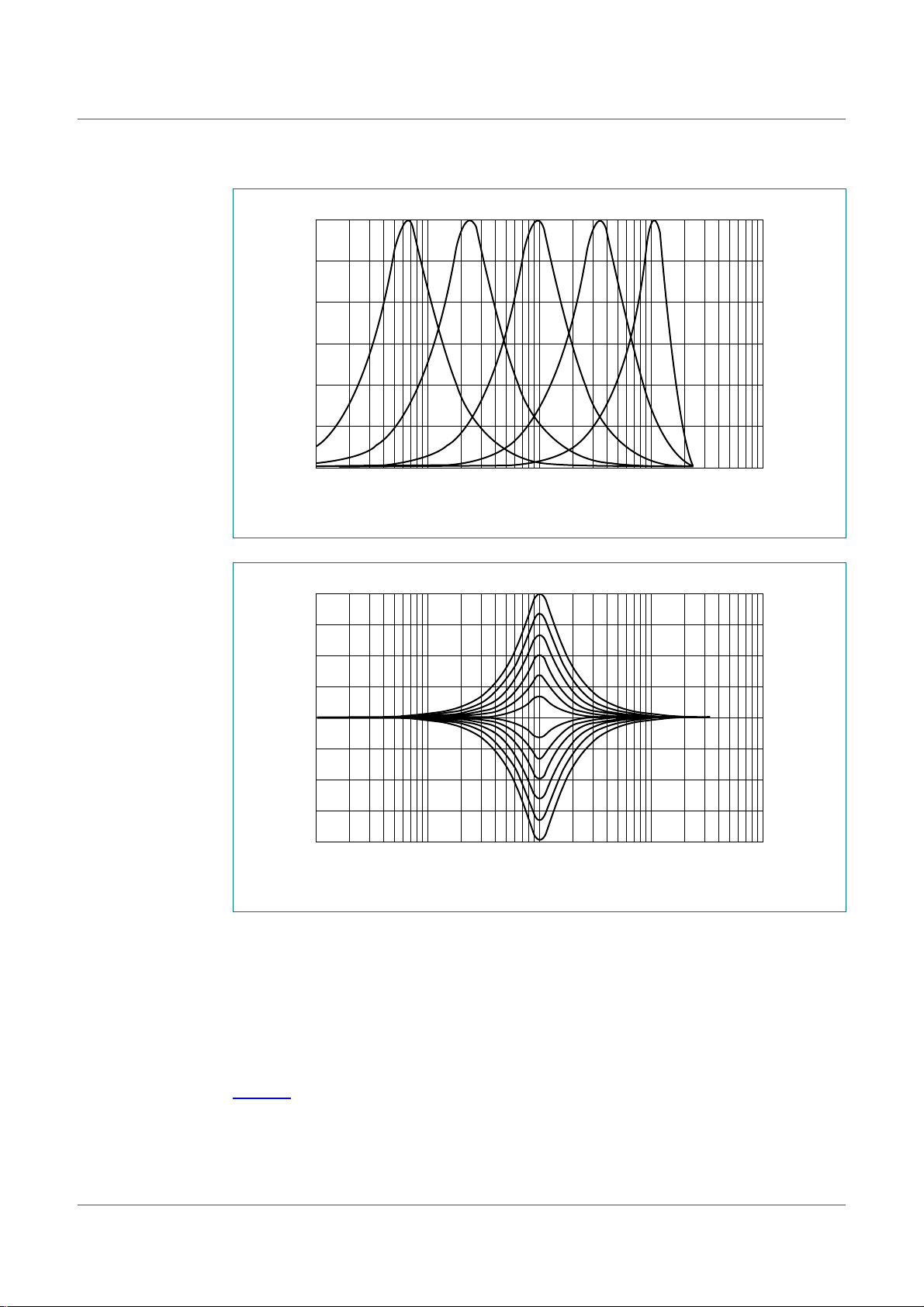
Figure 6, Figure 7 and Figure 8 show some of the possible transfer functions of the
equalizer bands. The relations are symmetrical for the suppression and amplification
functions. A skewing effect can be observed for the higher frequencies.
Different configurations are available for the same filter transfer function, thus allowing
optimum numerical noise performance. The binary filter configuration parameters t1and t
control the actual configuration and should be chosen according to Equation 6.
0 ω<=π 2⁄
t
=
1 ω>π 2⁄
1
0k2>=0
1k2<0
=
t
2
(5)
2
(6)
A maximum of 12 dB amplification per equalizer stage can be achievedwith respect to the
input signal. Each band of the equalizer is provided with a −6 dB amplification, so in order
to prevent numerical clipping for some filter settings with over 6 dB of amplification, band
filters can be scaled by 0 dB or −6 dB. For optimum numerical noise performance steps of
−6 dB amplification should be applied to the highest possible sections that are still within
scale signal processing safeguards. Band filters can be scaled with the binary parameters
listed in Table 14.
Table 14. Equalizer scale factor coding
s scale factor (dB)
00
1 −6
8.5.1.3 Equalizer band control
For compact representation with positive signed parameters, parameters k1’ and k2’ are
introduced in Equation 7.
The parameters k0, k1', k2', t1, t2 and s must be combined in two 16-bit control words,
word1 and word2, and must fit within the representation given in Table 15. Parameters k1'
and k2' are unsigned floating-point representations in Equation 8.
TFA9812_2 © NXP B.V. 2009. All rights reserved.
Preliminary data sheet Rev. 02 — 22 January 2009 18 of 66
Page 19
NXP Semiconductors
k1′
k2′
1k
– t11=
=
1k
+ t
1k
– t20=
=
1k
+ t
TFA9812
BTL stereo Class-D audio amplifier with I2S input
1
1
2
2
0=
1
(7)
1=
2
kxM2E–⋅
=
M1<
In Equation 8, M is the unsigned mantissa and E the negative signed exponent. For
example, in word2 bits [14:8] = [0111 010] represent k2' = (7/24) × 2−2 = 1.09375 10−1.
Table 15. Equalizer control word construction
Word Section Data
word1 15 t
1
word1 [14:4] 11 mantissa bits of k1’
word1 [3:0] Four exponent bits of k
word2 15 t
2
’
1
word2 [14:11] Four mantissa bits of k2’
word2 [10:8] Three exponents bits of k
word2 [7:1] k
0
’
2
word2 0 s
Section 9.5.4 shows the I2C address locations of the controls for various bands of the
equalizer.
010aaa222
Gain
(dB)
12
8
Q1 = 0.27
Q2 = 0.61
Q3 = 1.65
(8)
4
0
1
10
2
10
3
10
4
10
Frequency (Hz)
5
10
Fig 6. Transfer functions for several quality factors Q
TFA9812_2 © NXP B.V. 2009. All rights reserved.
Preliminary data sheet Rev. 02 — 22 January 2009 19 of 66
Page 20
NXP Semiconductors
TFA9812
BTL stereo Class-D audio amplifier with I2S input
12
Gain
(dB)
8
4
0
1
10
2
10
3
10
Fig 7. Transfer functions for several center frequencies f
12
Gain
(dB)
6
10
c
4
Frequency (Hz)
010aaa223
010aaa224
5
10
0
-6
-12
1
10
Fig 8. Transfer functions for several gain factors G
8.5.2 Digital volume control
In I2C control mode both audio channels have separate digital volume control. In Legacy
control mode the volume control of both channels is common and the volume control
setting depends on the supply voltage on the pin AVOL (32).
8-bit volume control is availableper channel. This is dB-linear down to −124 dB in steps of
0.5 dB. The last step of the volume control is mute.
Table 16 shows the various settings and their related channel suppression:
2
10
3
10
4
10
Frequency (Hz)
5
10
TFA9812_2 © NXP B.V. 2009. All rights reserved.
Preliminary data sheet Rev. 02 — 22 January 2009 20 of 66
Page 21

NXP Semiconductors
Table 16. Volume control channel suppression table
[7:0] control value (hexadecimal) Gain (dB)
00 0
01 −0.5
... steps of 0.5 dB
F7 −123.5
F8 −124
F9 mute
Section 9 shows the I2C address locations for the digital gain control for both channels.
In Legacy mode the pin AVOL (32) can be used to control the volume.
Voltage levels of 0.8 V to 2.8 V correspond linearly to control values of 00h (0 dB) to F9h
(mute). See Table 16.
TFA9812
BTL stereo Class-D audio amplifier with I2S input
An external pull-up resistor connected to the V
DDD(3V3)
volume of 0 dB. Pin AVOL has no function in I2C mode.
8.5.3 Soft mute and mute
Soft mute is available in I2C and in Legacy control modes: hard mute can be enabled only
in I2C control mode.
In I2C control mode the soft mute function smoothly reduces the gain setting for both
channels to mute level over a duration of 128/fs seconds. The smooth shape is
implemented as a raised cosine function. Soft demute results in a similar gain increase.
This implementation avoids audible plops.
A differentsoft mute and soft demute function is implemented in Legacy mode. This works
via the analog gain control under the control of pin AVOL. The analog volumecontrol input
signal is first-order low-pass filtered with a time constant of 10 ms in the digital domain.
Suddenly switching on or switching off volume by setting the control voltage to
> 2.8 Vor < 0.8 V respectively will result in a fading which lasts approximately 15 ms
(switching between 0 V and 3.3 V at AVOL).
In Legacy mode the soft demute function that is part of the automatic power-up sequence
is similar to the I2C mode soft demute function described above. The I2C control for the
soft and hard mute functions can be found In Section 9.
8.5.4 Output signal and word-select polarity control
can be applied to provide a default
In I2C control mode the TFA9812 can switch the polarity of the stereo output signal. The
effect is a 180 degree phase shift of both output signals.
The TFA9812 also has the option of switching the polarity of the WS signal. Without
polarity inversion the left audio signal is connected to channel 1 and the right audio signal
is connected to channel 2.
The I2C control for the polarity switch can be found in Section 9.5.1.
8.5.5 Gain boost and clip level control
An additional gain boost of +24 dB can be selected in the TFA9812. In Legacy mode this
feature can be selected with the GAIN pin, see Table 17.
TFA9812_2 © NXP B.V. 2009. All rights reserved.
Preliminary data sheet Rev. 02 — 22 January 2009 21 of 66
Page 22

NXP Semiconductors
Table 17. GAIN pin functionality
GAIN pin value Function
0 0 dB gain
1 +24 dB gain
The I2C controls for selecting the +24 dB gain can be found in Section 9.5.6. The GAIN
pin has no function In I2C mode.
The TFA9812 featuresalso specific gain settings which are related to < 0.5 %, 10 %, 20 %
or 30 % clipping at the output of the TFA9812. These clipping values are only valid under
the following conditions:
• The volume control is set to 0 dB.
• The gain boost is set to 0 dB.
• A 0 dBFs I
The I2C controls for selecting a specific clip level can be found in Section 9.5.6. In Legacy
mode the clip level is set to 10 %.
BTL stereo Class-D audio amplifier with I2S input
2
S input signal is obtained.
TFA9812
8.5.6 Output power limiter
Output power can be limited to three discrete levels with respect to the maximum power.
The maximum power output value is determined by the value of the high voltage supply.
Clipping levels (see Section 8.5.5) still apply to the maximum levels of reduced output
voltage swings.
In I2C control mode the same output power limiting levels can be selected, see
Section 9.5.6. In Legacy control mode two pins can be used to select the output power
limit level as shown in Table 18.
Table 18. Legacy mode output power limiter control
Pin value Function
ADSEL2/PLIM2 ADSEL1/PLIM1
0 0 Maximum power
0 1 Maximum power − 1.5 dB
1 0 Maximum power − 3.0 dB
1 1 Maximum power − 4.5 dB
8.5.7 PWM control for performance improvement
The PWM switching frequency of the TFA9812 is dependent on:
• The sampling frequency, f
• The sampling frequency setting, f
• The PWM switching frequency setting, f
.
s
(selected) (see Section 9.5.7).
s
(selected) (see Section 9.5.6).
sw
Equation 9 shows the relationship between these settings and the PWM carrier
frequency:
f
f
sw
TFA9812_2 © NXP B.V. 2009. All rights reserved.
Preliminary data sheet Rev. 02 — 22 January 2009 22 of 66
s
----------------------------
f
s selected)()
f
⋅=
sw selected()
(9)
Page 23

NXP Semiconductors
The selected PWM switching frequency is 400 kHz by default and can be set to 350 kHz,
700 kHz and 750 kHz in I2C control mode. In Legacy mode 400 kHz is the only option and
this scales linearly if 32 kHz or 48 kHz is used as fs.
Remark: The selected sample frequency, fs (selected) must be equal to the sample
frequency (fs) in I2C control mode.
Remark: The performance of AM radio reception can sometimes be improved by
selecting non-interfering frequencies for the PWM signal.
8.6 Class-D amplification
The Class-D power amplification of the PWM signal is carried out in two BTL power
stages. The output signal voltage level is determined by the values on the V
The power amplifiers can be explicitly put into 3-state mode by using the pin ENABLE as
shown in Table 19. The ENABLE pin is functional in Legacy mode and in I2C mode.
Table 19. ENABLE pin functionality
ENABLE pin value Function
0 Output stages in 3-state mode.
1 Switching enabled
TFA9812
BTL stereo Class-D audio amplifier with I2S input
pins.
DDP
[1]
.
[1] Can be overruled by a forced 3-state in Sleep or Fault mode.
8.7 Protection mechanisms
The TFA9812 has a wide range of protection mechanisms to facilitate optimal and safe
application. All of these are active in both I2C and Legacy control modes.
The following protections are included in the TFA9812:
• Thermal Foldback (TF)
• OverTemperature Protection (OTP)
• OverCurrent Protection (OCP)
• OverVoltage Protection (OVP)
• UnderVoltage Protection (UVP)
• Window Protection (WP)
• Lock Protection (LP)
• UnderFrequency Protection (UFP)
• OverFrequency Protection (OFP)
• Invalid BCK Protection (IBP)
• DC-blocking
• ESD
The reaction of the device to the different fault conditions differs per protection.
TFA9812_2 © NXP B.V. 2009. All rights reserved.
Preliminary data sheet Rev. 02 — 22 January 2009 23 of 66
Page 24

NXP Semiconductors
8.7.1 Thermal foldback
If the junction temperature of the TFA9812 exceeds the programmable Thermal foldback
threshold temperature the gain of the amplifier is decreased gradually to a level where the
combination of dissipation (P) and the thermal resistance from junction to ambient (R
results in a junction temperature around the threshold temperature.
This means that the device will not completely switch off, but remains operational at lower
output power levels. Especially with music output signals this feature enables high peak
output power while still operating without any external heat sink other than the
printed-circuit board area. If the junction temperature still increases due to external
causes, the OTP switches the amplifier to 3-state mode.
Under I2C control the Thermal foldback threshold temperature value can be lowered
(see Section 9.5.8): In Legacy control mode the default threshold value of 125 °C is fixed.
8.7.2 Overtemperature protection
This is a ‘hard’ protection to prevent heat damage to the TFA9812. The overtemperature
threshold level is the 160 °C junction temperature.
TFA9812
BTL stereo Class-D audio amplifier with I2S input
th(j-a)
)
When the threshold temperature is exceeded the output stages are set to 3-state mode.
The temperature is then checked at 1 µs intervals and the output stages will operate
normally again once the temperature has dropped below the threshold level.
OTP is flagged by a low DIAG pin. The TFA9812 temperature is an I2C reading, see
Section 9.5.9.
Under normal conditions thermal foldback prevents the overtemperature protection from
being triggered.
8.7.3 Overcurrent protection
The output current of the power amplifiers is current-limited. When an output stage
exceeds a current of 3 A typical, the output stages are set to 3-state mode and after 1 µs
the stages will start operating normally again. These interruptions are not audible.
OCP is flagged by a low DIAG pin and by a high DIAG I2C status bit, see Section 9.5.10.
I2C settings remain valid.
8.7.4 Overvoltage protection
The supply for the power stages (V
supply voltage exceeds 20 V the device will enter Sleep mode. When the supply voltage
has fallen below 20 V again the power-up sequence is started.
OVP is flagged by a low DIAG pin and by a high DIAG I2C status bit, see Section 9.5.10.
I2C settings remain valid.
DDA
, V
) is protected against overvoltage. When a
DDP
8.7.5 Undervoltage protections
The supplies are protected against undervoltage. When this is detected the device will
enter Sleep mode. When the supply voltage has risen to a sufficient level again the
power-up sequence is started.
Table 20 shows the UVP trigger levels for the V
TFA9812_2 © NXP B.V. 2009. All rights reserved.
Preliminary data sheet Rev. 02 — 22 January 2009 24 of 66
DDA
and V
DDA(3V3)
supplies:
Page 25

NXP Semiconductors
Table 20. Undervoltage trigger levels
Pin name UVP level DIAG pin (protection active)
V
DDA
V
DDA(3V3)
8.7.6 Overdissipation protection
When the output current of the power amplifiers exceeds a current value of 3 A and the
temperature is above 140 °C, overdissipation protection is activated and the device enters
Sleep mode. A restart will be initiated automatically when the two overdissipation
conditions are both changed to ‘false’.
Overdissipation is flagged by a low DIAG pin and by a high DIAG I2C status bit, see
Section 9.5.10.
Under normal conditions thermal foldback prevents overdissipation protection from being
triggered. I2C settings remain valid.
8.7.7 Window protection
TFA9812
BTL stereo Class-D audio amplifier with I2S input
Min Max
≥ 7 V < 8 V LOW
≥ 1.6 V < 3 V -
Window protection is a feature for protecting the device against shorts from the outputs to
the ground or supply lines. If during power-up one of the outputs is shorted to V
V
, power-up does not proceed any further. The trigger levels for these conditions are:
DDP
• OUTxx > V
DDA
− 1 V, or
• OUTxx < REFA + 1 V.
The WP alarm is flagged by a low DIAG pin and by a high DIAG I2C status bit, see
Section 9.5.10.
8.7.8 Lock protection
When the selected clockinput source (MCLK, BCK or crystal) stops running, the TFA9812
is able to detect this and set the output stages to 3-state mode. Without this protection
peripheral devices in an application might be damaged.
The PLL lock indication is an I2C reading and will be ‘false’ in the event of a clock
interruption, see Section 9.5.10.
8.7.9 Underfrequency protection
UFP sets the output stages to 3-state mode when the clock input source is too low. The
PWM switching frequency can becomes critically low when the clock input source is lower
than specified. Without UFP peripheral devices in an application might be damaged.
The status of the UFP is shown in I2C reading register, see Section 9.5.10.
SSPx
or
8.7.10 Overfrequency protection
OFP sets the output stages to 3-state mode when the clock input source is too high. The
PWM controller can become unstable when the clock input source is higher than
specified. Without OFP peripheral devices in an application might be damaged.
The status of the OFP is shown in I2C reading register, see Section 9.5.10.
TFA9812_2 © NXP B.V. 2009. All rights reserved.
Preliminary data sheet Rev. 02 — 22 January 2009 25 of 66
Page 26

NXP Semiconductors
8.7.11 Invalid BCK protection
The BCK clock signal is verified as being at one of the allowed relative frequencies: 32 fs,
48 fsor 64 fs. If it is not at one of these frequencies the TFA9812will set the output stages
to 3-state mode to prevent audible effects.
The MCLK clock signal is also verified as being valid, see Section 8.2.3.
Detection of violation results in an automatic internal overruling of the MCLK assignment
to BCK.
8.7.12 DC blocking
The TFA9812features a high pass filter after the I2S input to block DC signals. DC values
at the output can damage the peripheral devices. The high pass filter is always enabled.
8.7.13 Overview protections
Table 21 shows the overview of the protections.
Table 21. Overview protections
Protections
Symbol Conditions DIAG
TF programmable
OTP T
OCP I
OVP V
UVP V
ODP T
WP
LP PLL out of lock Floating LP Floating Restart (fault to operating
UFP PLL frequency < 45 MHz Floating UFP Floating Restart (fault to operating
max. T
> 160 °C LOW DIAG Floating Automatic, after 1 µs and
j
> I
O
ORM
> 20 V LOW DIAG Floating Restart (fault to operating
DDA
< 8 V or
DDA
V
DDA(3V3)
> 140 °C and IO>I
j
[2]
OUTX > V
OUTX < REFA + 1 V
> 125 °C
j
<3V
DDA
− 1 V or
TFA9812
BTL stereo Class-D audio amplifier with I2S input
I2C
pin
flag
Floating - Switching Automatic, increasing
LOW DIAG Floating Automatic, after 1 µs and
LOW DIAG Floating Restart (fault to operating
LOW DIAG Floating Restart (fault to operating
ORM
LOW DIAG Floating Restart (fault to operating
Output Recovering
[1]
volume control back to
volume setting
T
j
I
O<IORM
when V
V
DDA(3V3)
when V
V
DDA(3V3)
when T
IO < I
when OUTX < V
and OUTX > V
when PLL is in lock)
when
PLL frequency > 45 MHz)
< 160 °C
DDA
DDA
< 140 °C or
j
ORM
>3V)
>3V)
)
> 8 V and
> 8 V and
DDA
+1V)
SSA
− 1V
TFA9812_2 © NXP B.V. 2009. All rights reserved.
Preliminary data sheet Rev. 02 — 22 January 2009 26 of 66
Page 27

NXP Semiconductors
TFA9812
BTL stereo Class-D audio amplifier with I2S input
Table 21. Overview protections
Protections
Symbol Conditions DIAG
OFP PLL frequency > 140 MHz Floating OFP Floating Restart (fault to operating
IBP BCK/WS is not 32 ± 2,
48 2 or 64 2
[1] See, Section 9.5.10.
[2] Window Protection is only checked at power-up.
…continued
pin
Floating - Floating Restart (fault to operating
9. I2C bus interface and register settings
9.1 I2C bus interface
The TFA9812 supports the 400 kHz I2C bus microcontroller interfacemode standard. This
can be used to control the TFA9812 and to exchange data with it when in I2C control
mode, see Section 8.2.1.
The TFA9812 can operate in I2C slave mode only as slave receiver or a slave transmitter.
I2C
flag
Output Recovering
[1]
when
PLL frequency < 140 MHz)
when BCK/WS is 32 ± 2,
48 2 or 64 2)
The serial hardware interface involves the pins of the TFA9812 as described in Table 22.
Table 22. I2C pins in I2C control mode
Pin name Description
2
SCL/SFOR I
SDA/MS I
ADSEL2/PLIM2 I
ADSEL1/PLIM1 I
C bus clock input
2
C bus data input and output
2
C bus device address bit A2
2
C bus device address bit A1
Voltage values applied to the I2C bus device address pins are interpreted as described in
Table 23.
2
Table 23. I
Logic value Voltage A2/A1
0< V
1> V
C pin voltages in I2C control mode
IL
IH
9.2 I2C bus TFA9812 device addresses
Table 24 shows the register address options for the TFA9812 as part of the 8-bit byte that
contains the device address as well as the bit indicator read/write_not R/!W. The TFA9812
supports four different addresses, each of which can be configured using the pins
ADSEL1/PLIM1 and ADSEL2/PLIM2, see Table 22.
Table 24. I2C bus device address
(MSB) Bit (LSB)
11010A2A1R/!W
TFA9812_2 © NXP B.V. 2009. All rights reserved.
Preliminary data sheet Rev. 02 — 22 January 2009 27 of 66
Page 28

NXP Semiconductors
9.3 I2C write cycle description
Table 25 shows the cycle required for writing data to the I2C registers of the TFA9812. The
byte size is 8 bits. The I2C registers of the TFA9812 store two data bytes. Data is always
written in pairs of two bytes. Data transfer is always MSB first.
The cycle format for writing to the TFA9812 using SDA is as follows:
1. The microcontroller asserts a start condition (S).
2. The microcontroller sends the device address (7 bits) of the TFA9812 followed by the
3. The TFA9812 asserts an acknowledge (A).
4. The microcontroller writes the 8-bit TFA9812 register address to which the first data
5. The TFA9812 asserts an acknowledge.
6. The microcontroller sends the first byte. This is the most significant byte of the
7. The TFA9812 asserts an acknowledge.
8. The microcontroller sends the second byte.
9. The TFA9812 asserts an acknowledgement.
10. The microcontroller can either assert the stop condition (P) or continue with a further
TFA9812
BTL stereo Class-D audio amplifier with I2S input
R/!W bit set to 0.
byte will be written.
register.
pair of data bytes,repeating step 6. In the latter case the targeted register address will
have been auto-increased by the TFA9812.
Table 25. I2C write cycle
Start TFA9812
Address
S 11010A
R/!W TFA9812 first
register address
0 A ADDR A MS1 A LS1 <....> P
2A1
MS
databyte
LS
databyte
9.4 I2C read cycle description
Table 26 shows the cycle required for reading data from the I2C registers of the TFA9812.
The byte size is 8 bits. The I2C registers of the TFA9812 store two data bytes. Data is
always read in pairs of two bytes. Data transfer is always MSB-first.
The read cycle format for writing to the TFA9812 using SDA is as follows:
1. The microcontroller asserts a start condition (S).
2. The microcontroller sends the device address (7 bits) of the TFA9812 followed by the
R/!W bit set to 0.
3. The TFA9812 asserts an acknowledge (A).
4. The microcontroller writes the 8-bit TFA9812register address from which the first data
byte will be read.
5. The TFA9812 asserts an acknowledge.
6. The microcontroller asserts a repeated start (Sr).
7. The microcontroller resends the device address (7 bits) of the TFA9812 followed by
the R/!W bit set to 1.
8. The TFA9812 asserts an acknowledge.
More
data...
Stop
TFA9812_2 © NXP B.V. 2009. All rights reserved.
Preliminary data sheet Rev. 02 — 22 January 2009 28 of 66
Page 29

NXP Semiconductors
9. The TFA9812 sends the first byte. This is the most significant byte of the register.
10. The microcontroller asserts an acknowledge.
11. The TFA9812 sends the second byte.
12. The microcontroller asserts either an acknowledge or a negative acknowledge (NA).
Table 26. I2C read cycle
Start TFA9812
address
S 11010A
R/!W First
0 A ADDR A Sr 11010A2A11 A MS1 A LS1 <A> <....> NA P
2A1
9.5 Top-level register map
Table 27 describes the assignments of the various register addresses to the functional
control or status areas at top level. There are 47 control registers and 2 status registers.
TFA9812
BTL stereo Class-D audio amplifier with I2S input
– If the microcontroller has asserted an acknowledge, the targeted register address
is auto-increased by the TFA9812 and steps 9 to 12 are repeated.
– If the microcontroller has asserted a negative acknowledge,the TFA9812 frees the
I2C bus and the microcontroller generates a stop condition (P).
register
address
TFA9812
address
R/!W MS
data
byte
LS
data
byte
More
data...
More
data...
Stop
The following subsections give the individual register interpretations and bit level details.
Table 27. Top-level register map
Register
address
(hex)
0x00 0x0020;
0x01 0x0000 R/W
0x02 0x0006 R/W
0x03 0x0002 R/W
0x04 0x0058 R/W
0x05 0x4F40 R/W
0x06 0x0058 R/W
0x07 0x4F40 R/W
0x08 0x0A63 R/W
0x09 0x4240 R/W
0x0A 0x0A63 R/W
0x0B 0x4240 R/W
0x0C 0x00B7 R/W
0x0D 0x4E40 R/W
0x0E 0x00B7 R/W
0x0F 0x4E40 R/W
0x10 0x14A2 R/W
Default (hex) Access See: Description
Legacy_mode
2
0x0021; I
C_mode
R/W
Section 9.5.1 Interpolator settings and soft mute
Section 9.5.2 Volume control
Section 9.5.3 Format digital in
Section 9.5.4 Equalizer configuration
Section 9.5.5 Equalizer_A1 word_1; word_1 for
equalizer band A1, see
Section 9.5.5 Equalizer_A1 word_2; see
Section 8.5.1.2
Section 9.5.5 Equalizer_B1 word_1
Section 9.5.5 Equalizer_B1 word_2
Section 9.5.5 Equalizer_C1 word_1
Section 9.5.5 Equalizer_C1 word_2
Section 9.5.5 Equalizer_D1 word_1
Section 9.5.5 Equalizer_D1 word_2
Section 9.5.5 Equalizer_A2 word_1
Section 9.5.5 Equalizer_A2 word_2
Section 9.5.5 Equalizer_B2 word_1
Section 9.5.5 Equalizer_B2 word_2
Section 9.5.5 Equalizer_C2 word_1
Section 8.5.1.2
TFA9812_2 © NXP B.V. 2009. All rights reserved.
Preliminary data sheet Rev. 02 — 22 January 2009 29 of 66
Page 30

NXP Semiconductors
TFA9812
BTL stereo Class-D audio amplifier with I2S input
Table 27. Top-level register map
Register
address
(hex)
0x11 0x7A40 R/W Section 9.5.5 Equalizer_C2 word_2
0x12 0x14A2 R/W
0x13 0x7A40 R/W
0x14 0x0156 R/W
0x15 0x4D40 R/W
0x16 0x0156 R/W
0x17 0x4D40 R/W
0x18 0x2871 R/W
0x19 0x7140 R/W
0x1A 0x2871 R/W
0x1B 0x7140 R/W
0x1C 0x02A5 R/W
0x1D 0x4C40 R/W
0x1E 0x02A5 R/W
0x1F 0x4C40 R/W
0x20 0x4A80 R/W
0x21 0x5040 R/W
0x22 0x4A80 R/W
0x23 0x5040 R/W
0x24 0x0534 R/W
0x25 0x4B40 R/W
0x26 0x0534 R/W
0x27 0x4B40 R/W
0x28 0xD961 R/W
0x29 0x4840 R/W
0x2A 0xD961 R/W
0x2B 0x4840 R/W
0x2C 0x0005 R/W
0x2D 0x000E R/W
0x2E 0x0000 R/W
0x2F - R
0x30 - R
Default (hex) Access See: Description
…continued
Section 9.5.5 Equalizer_D2 word_1
Section 9.5.5 Equalizer_D2 word_2
Section 9.5.5 Equalizer_A3 word_1
Section 9.5.5 Equalizer_A3 word_2
Section 9.5.5 Equalizer_B3 word_1
Section 9.5.5 Equalizer_B3 word_2
Section 9.5.5 Equalizer_C3 word_1
Section 9.5.5 Equalizer_C3 word_2
Section 9.5.5 Equalizer_D3 word_1
Section 9.5.5 Equalizer_D3 word_2
Section 9.5.5 Equalizer_A4 word_1
Section 9.5.5 Equalizer_A4 word_2
Section 9.5.5 Equalizer_B4 word_1
Section 9.5.5 Equalizer_B4 word_2
Section 9.5.5 Equalizer_C4 word_1
Section 9.5.5 Equalizer_C4 word_2
Section 9.5.5 Equalizer_D4 word_1
Section 9.5.5 Equalizer_D4 word_2
Section 9.5.5 Equalizer_A5 word_1
Section 9.5.5 Equalizer_A5 word_2
Section 9.5.5 Equalizer_B5 word_1
Section 9.5.5 Equalizer_B5 word_2
Section 9.5.5 Equalizer_C5 word_1
Section 9.5.5 Equalizer_C5 word_2
Section 9.5.5 Equalizer_D5 word_1
Section 9.5.5 Equalizer_D5 word_2
Section 9.5.6 PWM signal control
Section 9.5.7 Digital-in clock configuration
Section 9.5.8 Thermal foldback control
Section 9.5.9 TFA9812 temperature
Section 9.5.10 Miscellaneous status
Reserved registers or bits will be indicated by RSD.
TFA9812_2 © NXP B.V. 2009. All rights reserved.
Preliminary data sheet Rev. 02 — 22 January 2009 30 of 66
Page 31

NXP Semiconductors
TFA9812
BTL stereo Class-D audio amplifier with I2S input
9.5.1 Interpolator settings and soft mute
Table 28. Register address 00h: miscellaneous I2C interpolator settings
Bit 15 14 13 12 11 10 9 8
Symbol RSD RSD RSD RSD RSD RSD RSD RSD
Default 00000000
Bit 7 6 5 4 3 2 1 0
Symbol RSD INV_POL ROFF1 ROFF0 FDEMP2 FDEMP1 FDEMP0 S_MUTE
Default 00100001/0
Table 29. Bit description of register 00h: miscellaneous I2C interpolator settings
Bit Symbol Description
6 INV_POL Enable polarity inversion:
0 = No polarity inversion (left audio signal connected to
channel 1; right signal to channel 2)
1 = Polarity inversion enabled
5 to 4 ROFF[1:0] Filter roll-off sharpness:
0 = Slow filter roll-off (2 to 8 f
1 = Slow filter roll-off (2 to 8 fs) ≥ stop band > 0.7619 f
2 = Fast filter roll-off (2 to 8 fs) ≥ stop band > 0.6094 f
3 = Fast filter roll-off (2 to 8 fs) ≥ stop band > 0.6094 f
3 to 1 FDEMP[2:0] Digital de-emphasis setting:
0 = No digital de-emphasis
1 = Digital de-emphasis for f
2 = Digital de-emphasis for f
3 = Digital de-emphasis for f
4 = Digital de-emphasis for f
5 to 8 = No digital de-emphasis
0 S_MUTE Soft mute:
0 = Soft mute disabled using raised cosine (default in
Legacy control mode)
1 = Soft mute enabled using raised cosine (default in
2
C control mode)
I
) ≥ stop band > 0.7619 f
s
= 32 kHz
s
= 44.1 kHz
s
= 48 kHz
s
= 96 kHz
s
s
s
s
s
9.5.2 Volume control
Table 30. Register address 01h: volume control
Bit 15 14 13 12 11 10 9 8
Symbol VOL_L7 VOL_L6 VOL_L5 VOL_L4 VOL_L3 VOL_L2 VOL_L1 VOL_L0
Default 00000000
Bit 7 6 5 4 3 2 1 0
Symbol VOL_R7 VOL_R6 VOL_R5 VOL_R4 VOL_R3 VOL_R2 VOL_R1 VOL_R0
Default 00000000
TFA9812_2 © NXP B.V. 2009. All rights reserved.
Preliminary data sheet Rev. 02 — 22 January 2009 31 of 66
Page 32

NXP Semiconductors
TFA9812
BTL stereo Class-D audio amplifier with I2S input
Table 31. Bit description of register 00h: miscellaneous I2C interpolator settings
Bit Symbol Description
15 to 8 VOL_L[15:8] See
7 to 0 VOL_R[7:0] See
Table 16 for suppression levels on left channel as
function of data byte setting.
Table 16 for suppression levels on right channel as
function of data byte setting.
9.5.3 Digital input format
Table 32. Register address 02h: digital input format
Bit 15 14 13 12 11 10 9 8
Symbol RSD RSD RSD RSD RSD RSD RSD RSD
Default 00000000
Bit 7 6 5 4 3 2 1 0
Symbol RSD RSD RSD RSD DI_FOR2 DI_FOR1 DI_FOR0 WS_POL
Default 00000110
Table 33. Bit description of register 02h: digital input format
Bit Symbol Description
3 to 1 DI_FOR[2:0] Digital audio input format:
0 = RSD
1 = RSD
2 = MSB-justified data up to 24 bits
2
S data up to 24 bits
3 = I
4 = LSB-justified 16-bit data
5 = LSB-justified 18-bit data
6 = LSB-justified 20-bit data
7 = LSB-justified 24-bit data
0 WS_POL Enable WS signal polarity inversion:
0 = No WS signal polarity inversion
1 = WS signal polarity inversion enabled
9.5.4 Equalizer configuration
Table 34. Register address 03h: equalizer configuration
Bit 15 14 13 12 11 10 9 8
Symbol RSD RSD RSD RSD RSD RSD RSD RSD
Default 00000000
Bit 7 6 5 4 3 2 1 0
Symbol RSD RSD RSD RSD RSD RSD EQ_BP EQ_BND
Default 00000010
TFA9812_2 © NXP B.V. 2009. All rights reserved.
Preliminary data sheet Rev. 02 — 22 January 2009 32 of 66
Page 33

NXP Semiconductors
TFA9812
BTL stereo Class-D audio amplifier with I2S input
Table 35. Bit description of register 03h: equalizer configuration
Bit Symbol Description
1 EQ_BP Equalizer bypass enable:
0 = Equalizer not bypassed
1 = Equalizer bypassed
0 EQ_BND Equalizer 10-band or 5-band configuration selection:
0 = 10-band equalizer configuration enabled
1 = 5-band equalizer configuration enabled
9.5.5 Equalizer settings
Table 36. Register addresses xxh = 04, 06...2A
For word1 for equalizer 'yy' see Figure 9
Bit 15 14 13 12 11 10 9 8
Symbol Eyy_t
Default
[1]
--------
Bit 7 6 5 4 3 2 1 0
Symbol Eyy_k
Default
[1]
--------
Eyy_k1m10 Eyy_k1m9 Eyy_k1m8 Eyy_k1m7 Eyy_k1m6 Eyy_k1m5 Eyy_k1m4
1
3 Eyy_k1m2 Eyy_k1m1 Eyy_k1m0 Eyy_k1e3 Eyy_k1e2 Eyy_k1e1 Eyy_k1e0
1m
[1] Default settings are shown in Table 27. The corresponding equalizer configuration is shown in Table 40.
Table 37. Register addresses xxh = 05, 07...2B
For word2 for equalizer 'yy' see Figure 9
Bit 15 14 13 12 11 10 9 8
Symbol Eyy_t
Eyy_k2m3 Eyy_k2m2 Eyy_k2m1 Eyy_k2m0 Eyy_k2e2 Eyy_k2e1 Eyy_k2e0
2
Default -------Bit 7 6 5 4 3 2 1 0
Symbol Eyy_k
6 Eyy_k05 Eyy_k04 Eyy_k03 Eyy_k02 Eyy_k01 Eyy_k00 Eyy_s
0
Default --------
[1] Default settings are shown in Table 27. The corresponding equalizer configuration is shown in Table 40.
TFA9812_2 © NXP B.V. 2009. All rights reserved.
Preliminary data sheet Rev. 02 — 22 January 2009 33 of 66
Page 34

NXP Semiconductors
TFA9812
BTL stereo Class-D audio amplifier with I2S input
Left in
Right in
A1
C1
B1
D1 D2 D3 D4 D5
A2 A3 A4 A5
C2 C3 C4 C5
B2 B3 B4 B5
Fig 9. Equalizer configuration and register location mapping
Table 38. Bit description of registers xxh = 04, 06...2A
Bit Symbol Description
15 Eyy_t
14 to 4 Eyy_k1
1
[10:0] The 11 mantissa bits of the filter parameter k1, see
m
The filter configuration bit t1, see Section 8.5.1.2.
Section 8.5.1.2.
3 to 0 Eyy_k1
[3:0] The four exponent bits of the filter parameter k1, see
e
Section 8.5.1.2.
Left out
2 × 5 or 2 × 10
Right out
2 × 5 or 2 × 10
010aaa404
Table 39. Bit description of registers xxh = 05, 07...2B
Bit Symbol Description
15 Eyy_t
14 to 11 Eyy_k
2
[3:0] The four mantissa bits of the filter parameter k2, see
2m
The filter configuration bit t2, see Section 8.5.1.2.
Section 8.5.1.2.
10 to 8 Eyy_k
[2:0] The three exponent bits of the filter parameter k2, see
2e
Section 8.5.1.2.
7 to 1 Eyy_k
[6:0] The seven bits of the filter gain parameter k0, see
0
Section 8.5.1.2.
0 Eyy_s The filter scale-factor bits, see
Section 8.5.1.2:
0 = No scaling applied
1 = −6 dB amplification enabled
TFA9812_2 © NXP B.V. 2009. All rights reserved.
Preliminary data sheet Rev. 02 — 22 January 2009 34 of 66
Page 35

NXP Semiconductors
TFA9812
BTL stereo Class-D audio amplifier with I2S input
Table 40. Default configuration equalizer for fs = 44.1 kHz
Band A1/B1 A2/B2 A3/B3 A4/B4 A5/B5 C1/D1 C2/D2 C3/D3 C4/D4 C5/D5
Frequency
(Hz)
Q-factor 1111111111
Gain (dB) 0000000000
31 63 125 250 500 1000 2000 4000 8000 16000
9.5.6 PWM signal control
Table 41. Register 2Ch: PWM signal control
Bit 15 14 13 12 11 10 9 8
Symbol RSD RSD RSD RSD RSD RSD RSD RSD
Default 00000000
Bit 7 6 5 4 3 2 1 0
Symbol RSD PLIM1 PLIM0 PW_OFF PW_SF1 PW_SF0 PW_CL1 PW_CL0
Default 00000101
Table 42. Bit description address 2Ch
Bit Symbol Description
7 GAIN +24 dB gain boost:
0 = Gain boost 0 dB
1 = Gain boost +24 dB
6 to 5 PLIM[1:0] Output power limitation:
0 = Maximum power
1 = Maximum power − 1.5 dB
2 = Maximum power − 3.0 dB
3 = Maximum power − 4.5 dB
4 PW_OFF Hard mute control:
0 = No hard mute
1 = Hard mute enabled, implemented by PWM signal
with 50 % duty cycle
3 to 2 PW_SF[1:0] PWM switching frequency:
0 = 350 kHz
1 = 400 kHz
2 = 700 kHz
3 = 750 kHz
1 to 0 PW_CL[1:0] PWM clip level:
0 = < 0.5 % THD
1 = 10 % THD
2 = 20 % THD
3 = 30 % THD
TFA9812_2 © NXP B.V. 2009. All rights reserved.
Preliminary data sheet Rev. 02 — 22 January 2009 35 of 66
Page 36

NXP Semiconductors
TFA9812
BTL stereo Class-D audio amplifier with I2S input
9.5.7 Digital-in clock configuration
Table 43. Register 2Dh: digital-in clock configuration
Bit 15 14 13 12 11 10 9 8
Symbol RSD RSD RSD RSD RSD RSD RSD RSD
Default 00000000
Bit 7 6 5 4 3 2 1 0
Symbol RSD RSD RSD FSUB3 FSUB2 FSUB1 FSUB0 DI_MS
Default 00001110
Table 44. Bit description of register 2Dh:digital-in clock configuration
Bit Symbol Description
4 to 1 FSUB[3:0] Sample frequency f
0 = 8 kHz
1 = 11.025 kHz
2 = 12 kHz
3 = 16 kHz
4 = 22.05 kHz
5 = 24 kHz
6 = 32 kHz
7 = 44.1 kHz
8 = 48 kHz
9 = 64 kHz
10 = 88.2 kHz
11 = 96 kHz
12 = 128 kHz
13 = 176.4 kHz
14 = 192 kHz
15 = RSD
0 DI_MS TFA9812 digital-in Master/Slave mode selection:
0 = Slave mode
1 = Master mode
of digital-in signal:
s
9.5.8 Thermal foldback control
Table 45. Register 2Eh: thermal foldback control
Bit 15 14 13 12 11 10 9 8
Symbol RSD RSD RSD RSD RSD RSD TP_THR9 TP_THR8
Default 00000000
Bit 7 6 5 4 3 2 1 0
Symbol TP_THR7 TP_THR6 TP_THR5 TP_THR4 TP_THR3 TP_THR2 TP_THR1 TP_THR0
Default 00000000
TFA9812_2 © NXP B.V. 2009. All rights reserved.
Preliminary data sheet Rev. 02 — 22 January 2009 36 of 66
Page 37

NXP Semiconductors
TFA9812
BTL stereo Class-D audio amplifier with I2S input
Table 46. Bit description of register 2Dh: digital-in clock configuration
Bit Symbol Description
9 to 0 TP_THR[9:0] Reduction on the maximum temperature of 125 °C.
The reduction can be calculated by:
reduction INTEGER
(TP_THR[9:0]
-----------------------------------
2.4552
in °C=
9.5.9 TFA9812 temperature
Table 47. Register 2Fh: TFA9812 temperature
Bit 15 14 13 12 11 10 9 8
Symbol RSD RSD RSD RSD RSD RSD TEMP9 TEMP8
Default -------Bit 7 6 5 4 3 2 1 0
Symbol TEMP7 TEMP6 TEMP5 TEMP4 TEMP3 TEMP2 TEMP1 TEMP0
Default --------
Table 48. Bit description of register 2Dh: digital-in clock configuration
Bit Symbol Description
9 to 0 TEMP[9:0] Temperature of the TFA9812, which can be calculated in
°C using: Temp TFA9812 = (1023 − TEMP[9:0]) / 2.4552
9.5.10 Miscellaneous status
Table 49. Register 30h: miscellaneous status
Bit 15 14 13 12 11 10 9 8
Symbol RSD RSD RSD RSD RSD RSD RSD RSD
Default -------Bit 7 6 5 4 3 2 1 0
Symbol RSD OFP UFP UVP1V8 UVP3V3 DIAG LP MUTE
Default --------
Table 50. Bit description of register 30h: miscellaneous status
Bit Symbol Description
6 OFP PLL frequency-over-range indicator:
0 = PLL frequency in supported range
1 = PLL frequency exceeds highest supported
frequency value
5 UFP PLL frequency under-range indicator:
0 = PLL frequency in supported range
1 = PLL frequency below lowest supported frequency
value
4 UVP1V8 Undervoltage detector for pins 4 and 41:
0 = No UVP has been detected
1 = A UVP has been detected since the last read-out of
the register
TFA9812_2 © NXP B.V. 2009. All rights reserved.
Preliminary data sheet Rev. 02 — 22 January 2009 37 of 66
Page 38

NXP Semiconductors
TFA9812
BTL stereo Class-D audio amplifier with I2S input
Table 50. Bit description of register 30h: miscellaneous status
…continued
Bit Symbol Description
3 UVP3V3 Undervoltage detector for pins 3 and 40:
0 = No UVP has been detected
1 = A UVP has been detected since the last read-out of
the register
[1]
2 DIAG Diagnostic pin flagging status
:
0 = Diagnostic pin has not been flagged low
1 = Diagnostic pin has been flagged low since the last
read-out of the register
1 LP PLL lock protection indicator:
0 = PLL is in locked status
1 = PLL is not in locked status
0 MUTE Soft mute status:
0 = No soft-mute or soft mute/demute in progress
1 = Audio signal muted as result of a soft mute
[1] The diagnostic pin 30 DIAG is flagged when several protection mechanisms have been active, see
Section 8.7.
9.6 Overview of functional control in each control mode
Table 51 shows the control level supported by either I2C or Legacy control mode for all
functions described in Section 9. It summarizes the information provided in the detailed
description of each function.
Table 51. Functional control support in I2C and Legacy control modes
D = fixed control setting, determined by default I2C register setting; N = not supported; Y = fully
supported (i.e. all options implemented in the TFA9812).
Control function Reference I2C mode Legacy mode
2
C register content Section 9 Y N/D
I
Sleep mode enable
Operating mode enable
3-state mode enable
2
Master/Slave I
S Section 8.2.3 YY
MCLK/BCK master input clock selection
Digital audio input format selection
Selection f
= 8 kHz to192 kHz Section 8.4.1 YD
s
Equalizer enable and configuration Section 8.5.1 YD
Section 8.2.2 YY
Section 8.2.2 YY
Section 8.2.2 YY
Section 8.2.3 Auto Auto
Section 8.4 Y Subset
[1]
[2]
Detailed equalizer settings Section 8.5.1 YN
Digital volume control per channel
Analog volumecontrol (shared for two channels)
De-emphasis for subset of allowed f
s
Soft mute
Section 8.5.2 YN
Section 8.5.3 NY
Section 8.5.3 YN
Section 8.5.3 YY
[3]
Hard mute Section 8.5.3 YN
Polarity switch enable
+24 dB gain boost
Section 8.5.4 YN
Section 8.5.6 YY
TFA9812_2 © NXP B.V. 2009. All rights reserved.
Preliminary data sheet Rev. 02 — 22 January 2009 38 of 66
Page 39

NXP Semiconductors
TFA9812
BTL stereo Class-D audio amplifier with I2S input
Table 51. Functional control support in I
D = fixed control setting, determined by default I2C register setting; N = not supported; Y = fully
supported (i.e. all options implemented in the TFA9812).
Control function Reference I2C mode Legacy mode
Clip level control Section 8.5.5 YD
Output power limit level control Section 8.5.6 YY
PWM signal frequency selection
Thermal foldback threshold temperature control Section 8.7.1 YN
[1] 32 kHz, 44.1 kHz and 48 kHz supported
[2] Bypass.
[3] Special Legacy mode implementation.
[4] 10 % clip level.
[5] 400 kHz.
10. Internal circuitry
Table 52. Internal circuitry
Pin Symbol Equivalent circuitry
1 XTALIN
32 AVOL
2
C and Legacy control modes
Section 8.5.7 YD
1, 32
ESD
V
, V
SS1
, REFA, REFD
SS2
Exposed die paddle
…continued
[4]
[5]
010aaa459
2 XTALOUT
3V
40 V
DDA(3V3)
DDD(3V3)
STABA
2
ESD
V
, V
SS2
, REFA, REFD,
SS2
, REFA, REFD,
010aaa460
010aaa461
3, 40
ESD
SS1
Exposed die-paddle
V
, V
SS1
Exposed die-paddle
TFA9812_2 © NXP B.V. 2009. All rights reserved.
Preliminary data sheet Rev. 02 — 22 January 2009 39 of 66
Page 40
NXP Semiconductors
TFA9812
BTL stereo Class-D audio amplifier with I2S input
Table 52. Internal circuitry
…continued
Pin Symbol Equivalent circuitry
4 STABA
41 STABD
4, 41
ESD
5 REFA
6V
DDA
6
5
7 TEST1
7
V
DDA(3V3), VDDD(3V3)
V
SS1, VSS2
Exposed die-paddle
24 V
V
SS1
Exposed die-paddle
V
DDA
13 kΩ
, REFA, REFD,
010aaa462
, REFD, V
SS2
010aaa463
,
9 STAB2
28 STAB1
10/11 V
18/19 V
26/27 V
SSP2
DDP
SSP1
12 BOOT2N
15 BOOT1P
22 BOOT2P
25 BOOT1N
9, 28
10/11, 26/27
12, 15, 22, 25
V
SS1
010aaa464
V
DDA
12 V
V
SS1
010aaa465
18/19
24 V
010aaa466
12 V
OUT2N, OUT1P, OUT2P, OUT1N
010aaa467
TFA9812_2 © NXP B.V. 2009. All rights reserved.
Preliminary data sheet Rev. 02 — 22 January 2009 40 of 66
Page 41

NXP Semiconductors
TFA9812
BTL stereo Class-D audio amplifier with I2S input
Table 52. Internal circuitry
…continued
Pin Symbol Equivalent circuitry
13/14 OUT2N
16/17 OUT1P
20/21 OUT2P
23/24 OUT1N
13/14, 16/17, 20/21, 23/24
29 DIAG
30 CDELAY
V
DDA
V
DDP
, V
V
SSP1
SSP2
010aaa468
V
DDA
29
V
SS1
V
SS1
010aaa469
31 POWERUP
33 ENABLE
34 GAIN
35 CSEL
36 ADSEL2/PLIM2
37 ADSEL1/PLIM1
43 TEST2
30
V
DDA
31
33, 34, 35, 36, 37, 43
Pull-down
50 µA
2 µA
200 nA 5 kΩ
DISCHARGE
V
SS1
3 kΩ
010aaa471
ESD
V
, V
SS1
Exposed die-paddle
, REFA, REFD,
SS2
010aaa472
010aaa470
250 nA
V
SS1
TFA9812_2 © NXP B.V. 2009. All rights reserved.
Preliminary data sheet Rev. 02 — 22 January 2009 41 of 66
Page 42
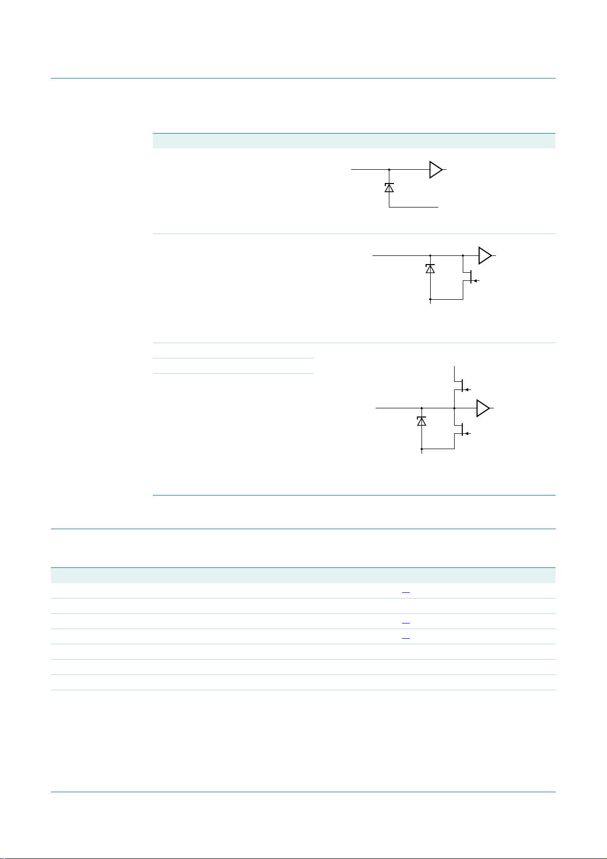
NXP Semiconductors
TFA9812
BTL stereo Class-D audio amplifier with I2S input
Table 52. Internal circuitry
…continued
Pin Symbol Equivalent circuitry
38 SCL/SFOR
38, 44
39 SDA/MS
39
45 WS
46 BCK
47 MCLK
45, 46, 47
ESD
V
V
SS1
Exposed die-paddle
ESD
, V
SS1
, REFA, REFD,
SS2
Exposed die-paddle
V
ESD
, V
SS2
DDD(3V3)
, REFA, REFD,
010aaa473
010aaa474
VSS1, VSS2, REFA, REFD,
Exposed die-paddle
010aaa475
11. Limiting values
Table 53. Limiting values
In accordance with the Absolute Maximum Rating System (IEC 60134).
Symbol Parameter Conditions Min Max Unit
V
DDA
V
DDP
V
DDA(3V3)
V
DDD(3V3)
T
j
T
stg
T
amb
analog supply voltage −V
power supply voltage −V
analog supply voltage (3.3 V) −V
digital supply voltage (3.3 V) −V
SS
; x = 1.2 −0.3 +24 V
SSPx
SS
SS
junction temperature - 150 °C
storage temperature −55 +150 °C
ambient temperature −40 +85 °C
P power dissipation 5 W
[1]
−0.3 +24 V
[1]
−0.3 +4.6 V
[1]
−0.3 +4.6 V
TFA9812_2 © NXP B.V. 2009. All rights reserved.
Preliminary data sheet Rev. 02 — 22 January 2009 42 of 66
Page 43

NXP Semiconductors
TFA9812
BTL stereo Class-D audio amplifier with I2S input
Table 53. Limiting values
…continued
In accordance with the Absolute Maximum Rating System (IEC 60134).
Symbol Parameter Conditions Min Max Unit
V
x
voltage on pin x DIAG
POWERUP
ENABLE, GAIN, CSEL,
[1]
VSS− 0.3 VSS + 12 V
[1]
VSS− 0.3 V
[1]
VSS− 0.5 VSS + 5.5 V
+ 0.3 V
DDA
ADSEL2/PLIM2,
ADSEL2/PLIM1,SCL/SFOR,
SDA/MS, DATA, WS, BCK,
MCLK
[1]
AVOL
V
esd
electrostatic discharge voltage according to the human body model
STAB1 and STAB2 with
VSS− 0.5 VSS + 4.6 V
−1750 +1750 V
respect to other pins
all other pins −2+2 kV
according to the charge
−500 +500 V
device model
[1] Vss = V
SS1
= V
= REFA = REFD
SS2
12. Thermal characteristics
Table 54. Thermal Characteristics
Symbol Parameter Condition Min Typ Max Unit
R
th(j-a)
R
th(j-c)
R
th(j-lead)
thermal resistance
from junction to
ambient
thermal resistance
from junction to case
thermal resistance
from junction to lead
No air flow, JEDEC board
No air flow; typical 4L board in
the NXP 4L reference
application
No air flow; typical 2L board in
the NXP 2L reference
application
Worst-case pin 5 - - K/W
[1][2]
- - 42 K/W
[2]
- - 36 K/W
[2]
- - 42 K/W
[3]
5 - - K/W
[1] Measured in a JEDEC high K-factor test board (standard EIA/JESD 51-7).
[2] Measured in free air with natural convection.
[3] Strongly depends on where measurement is made on the case: worst-case value stated.
TFA9812_2 © NXP B.V. 2009. All rights reserved.
Preliminary data sheet Rev. 02 — 22 January 2009 43 of 66
Page 44

NXP Semiconductors
TFA9812
BTL stereo Class-D audio amplifier with I2S input
13. Characteristics
13.1 DC Characteristics
Table 55. DC characteristics
Unless specified otherwise, V
V
SS1=VSS2
= REFD = REFA = 0 V, T
DDA=VDDP
MCLK clock mode, typical application diagram (
Symbol Parameter Condition Min Typ Max Unit
Supply voltage
V
DDA
analog supply
voltage
V
DDP
V
DDA(3V3)
power supply voltage 8 12 20 V
analog supply
voltage (3.3 V)
V
DDD(3V3)
digital supply voltage
(3.3 V)
I
P
I
DDA(3V3)
supply current soft mute mode, with
analog supply
current (3.3 V)
I
DDD(3V3)
digital supply current
(3.3 V)
Amplifier output pins; pins OUT1P, OUT1N, OUT2P and OUT2N
|V
| output offset voltage soft mute mode - - 5 mV
O(offset)
Power-up pin
V
IH
HIGH-level input
voltage
V
IL
LOW-level input
voltage
I
I
input current - 0.1 20 µA
MCLK, BCK, WS, DATA pin
V
IH
HIGH-level input
voltage
V
IL
LOW-level input
voltage
C
i
TFA9812_2 © NXP B.V. 2009. All rights reserved.
Preliminary data sheet Rev. 02 — 22 January 2009 44 of 66
input capacitance - - 3 pF
= 12 V, V
=25°C, RL=8Ω, fi= 1 kHz, fs= 44.1 kHz, fsw = 400 kHz, 24-bit I2S input data,
amb
SSP1
= V
SSP2
= 0 V, V
DDA(3V3)=VDDD(3V3)
= 3.3 V,
Figure 13).
81220V
3.0 3.3 3.6 V
3.0 3.3 3.6 V
[1]
-3845mA
load, filter and snubbers
connected
sleep mode
[1]
- 160 270 µA
operating mode
2
S slave mode - 2 4 mA
I
2
S master mode - 4 6 mA
I
sleep mode
V
DDA=VDDP
V
DDA=VDDP
=12V - 120 - µA
=1V - 40 70 µA
operating mode
2
S slave mode - 15 25 mA
I
2
S master mode - 25 40 mA
I
sleep mode;
-430µA
DATA=WS=BCK=
MLCK = 0 V
With respect to V
With respect to V
With respect to V
With respect to V
SS1
SS1
SS2
SS2
2.1 - V
DDD(3V3)
−0.3 - +0.8 V
0.7 × V
DDD(3V3)
- - 0.3 × V
-- V
DDD(3V3)
V
V
Page 45

NXP Semiconductors
TFA9812
BTL stereo Class-D audio amplifier with I2S input
Table 55. DC characteristics
Unless specified otherwise, V
V
SS1=VSS2
= REFD = REFA = 0 V, T
MCLK clock mode, typical application diagram (
…continued
DDA=VDDP
amb
= 12 V, V
SSP1
= V
SSP2
= 0 V, V
DDA(3V3)=VDDD(3V3)
= 3.3 V,
=25°C, RL=8Ω, fi= 1 kHz, fs= 44.1 kHz, fsw = 400 kHz, 24-bit I2S input data,
Figure 13).
Symbol Parameter Condition Min Typ Max Unit
V
OH
HIGH-level output
At IOH = −0.4 mA V
DDD(3V3)
− 0.4 V - - V
voltage
V
OL
LOW-level output
At IOL = 4 mA - - 400 mV
voltage
C
L
load capacitance - - 50 pF
SDA/MS, SCL/SFOR pin
V
IH
HIGH-level input
With respect to V
SS2
0.7 × V
DDD(3V3)
- 5.5 V
voltage
V
IL
LOW-level input
With respect to V
SS2
−0.3 - 0.3 × V
DDD(3V3)
V
voltage
V
hys(i)
input hysteresis
With respect to V
SS2
0.1 × V
DDD(3V3)
-- V
voltage
C
i
V
OL
input capacitance - - 2.5 pF
LOW-level output
At IOL = 3 mA - - 400 mV
voltage
ENABLE, GAIN, CSEL, ADSEL2/PLIM2, ASEL1/PLIM1 pin
V
IH
HIGH-level input
With respect to V
SS2
0.7 × V
DDD(3V3)
-- V
voltage
V
IL
LOW-level input
With respect to V
SS2
- 0.3 × V
DDD(3V3)
V
voltage
V
hys(i)
input hysteresis
With respect to V
SS2
0.1 × V
DDD(3V3)
-- V
voltage
I
I
input current - 50 93 µA
Regulators
V
o
output voltage STAB1 − V
STAB2 − V
SS1
SS1
10 11 12 V
10 11 12 V
STABA − REFA 1.65 1.8 1.95 V
STABD − REFD 1.65 1.8 1.95 V
CDELAY pin
V
CDELAY
voltage on pin
CDELAY
Relative to positive
analog power supply
-V
−1- V
DDA
Crystal pins
V
o(xtal)(p-p)
peak-to-peak crystal
With respect to V
SS2
- 1.8 - V
oscillator output
voltage
AVOL pin
V
i
input voltage Mute level, with respect
to V
SS2
0 dB level with respect
to V
SS2
I
I
input current - - 1 µA
0.77 0.8 0.83 V
2.74 2.8 2.86 V
TFA9812_2 © NXP B.V. 2009. All rights reserved.
Preliminary data sheet Rev. 02 — 22 January 2009 45 of 66
Page 46

NXP Semiconductors
TFA9812
BTL stereo Class-D audio amplifier with I2S input
Table 55. DC characteristics
Unless specified otherwise, V
V
SS1=VSS2
= REFD = REFA = 0 V, T
MCLK clock mode, typical application diagram (
…continued
DDA=VDDP
amb
= 12 V, V
SSP1
= V
SSP2
= 0 V, V
DDA(3V3)=VDDD(3V3)
= 3.3 V,
=25°C, RL=8Ω, fi= 1 kHz, fs= 44.1 kHz, fsw = 400 kHz, 24-bit I2S input data,
Figure 13).
Symbol Parameter Condition Min Typ Max Unit
Thermal Foldback (TF)
T
act(th_fold)
thermal foldback
[2]
118 125 132 °C
activation
temperature
OverTemperature Protection (OTP)
T
act(th_prot)
thermal protection
- - 160 °C
activation
temperature
OverVoltage Protection (OVP)
V
P(ovp)
overvoltage
20 22.3 24 V
protection supply
voltage
UnderVoltage Protections (UVP)
V
P(uvp)
undervoltage
protection supply
voltage
UVP on V
UVP on V
DDA
DDA(3V3)
7 7.5 8 V
1.6 2.2 3.0 V
OverCurrent Protection (OCP)
I
O(ocp)
overcurrent
[3]
3.0 3.3 3.6 A
protection output
current
Window Protection (WP)
V
o
output voltage high level - V
− 1- V
DDA
low level - REFA + 1 - V
OverFrequency Protection (OFP)
f
OFP
Overfrequency
At PLL output frequency
[4]
100 140 185 MHz
protection frequency
UnderFrequency Protection (OFP)
f
UFP
Underfrequency
At PLL output frequency
[4]
30 45 60 MHz
protection frequency
[1] IP is the current through the analog supply voltage (V
[2] Thermal foldback temperature sensor is not located at hottest spot. Hottest spot is 12 °C higher.
[3] Current limiting concept: in overcurrent condition no interruption of the audio signal in case of impedance drop.
[4] PLL output frequency not external available.
TFA9812_2 © NXP B.V. 2009. All rights reserved.
Preliminary data sheet Rev. 02 — 22 January 2009 46 of 66
) pin added to the current through the power supply voltage (V
DDA
DDP
) pin.
Page 47

NXP Semiconductors
13.2 AC characteristics
TFA9812
BTL stereo Class-D audio amplifier with I2S input
Table 56. AC characteristics
Unless specified otherwise, V
f
= 1 kHz, fs= 44.1 kHz, fsw= 400 kHz, 24-bit I2S input data, MCLK clock mode, typical application diagram (Figure 13).
i
DDA=VDDP
= 12 V, V
DDA(3V3)=VDDD(3V3)
= 3.3 V, T
=25°C, Rs < 0.1
amb
[1]
Ω
, RL=8Ω,
Symbol Parameter Condition Min. Typ. Max. Unit
Output power per channel
P
o(RMS)
RMS output power Continuous time output power per channel; THD = 1 %, RL = 6 Ω
= V
V
DDA
V
DDA
Continuous time output power per channel; THD = 10 %, R
V
DDA
Short time (≤ 10 s) output power per channel; THD = 10 %, R
V
DDA
Continuous time output power per channel; THD = 1 %, R
V
DDA
V
DDA
Continuous time output power per channel; THD = 10 %, R
V
DDA
V
DDA
V
DDA
Short time (≤ 10 s) output power per channel; THD = 10 %, R
V
DDA
= 12 V - 7.9 - W
DDP
= V
= 15 V - 12 - W
DDP
= V
= 12 V - 9.7 - W
DDP
= V
= 15 V - 15 - W
DDP
= V
= 12 V - 6.6 - W
DDP
= V
= 15 V - 10 - W
DDP
= V
= 12 V - 8.3 - W
DDP
= V
= 13.5 V - 10 - W
DDP
= V
= 15 V - 12 - W
DDP
= V
= 17 V - 15 - W
DDP
= 6 Ω
L
= 8 Ω
L
= 8 Ω
L
= 6 Ω
L
= 8 Ω
L
Performance
THD+N total harmonic
= 1 W; AES17 brick wall filter - 0.07 0.1 %
P
O
distortion-plus-noise
S/N signal-to-noise ratio V
V
n(o)
output noise voltage MCLK clock jitter < 200 ps; AES17 brick-wall filter
= 10 V; A-weighted - 103 - dB
O
operating mode - 70 - µV
soft mute mode - 70 - µV
hard mute mode - 30 - µV
α
cs
channel separation P
SVRR supply voltage ripple rejection V
η
po
output power efficiency RL = 8 Ω; P
= 1 W; aggressor channel:
o(RMS)
f
= 1 kHz
i
= 2 Vpp; f
ripple
= 6 Ω; P
R
L
o(RMS)
o(RMS)
ripple
= 8.3 W
= 9.7 W
50 54 - dB
= 100 Hz 55 60 - dB
[2]
-88-%
[2]
-83-%
Power-up times and delay times
t
d(on)
turn-on delay time - - 155 ms
TFA9812_2 © NXP B.V. 2009. All rights reserved.
Preliminary data sheet Rev. 02 — 22 January 2009 47 of 66
Page 48

NXP Semiconductors
TFA9812
BTL stereo Class-D audio amplifier with I2S input
Table 56. AC characteristics
Unless specified otherwise, V
f
= 1 kHz, fs= 44.1 kHz, fsw= 400 kHz, 24-bit I2S input data, MCLK clock mode, typical application diagram (Figure 13).
i
…continued
DDA=VDDP
= 12 V, V
DDA(3V3)=VDDD(3V3)
= 3.3 V, T
=25°C, Rs < 0.1
amb
[1]
Ω
, RL=8Ω,
Symbol Parameter Condition Min. Typ. Max. Unit
t
PD
propagation delay fs =
8 kHz - 3.6 - ms
11.025 kHz - 2.58 - ms
12 kHz - 2.39 - ms
16 kHz - 1.78 - ms
22.05 kHz - 1.3 - ms
24 kHz - 1.18 - ms
32 kHz - 892 - µs
44.1 kHz - 664 - µs
48 kHz - 600 - µs
64 kHz - 458 - µs
88.2 kHz - 320 - µs
96 kHz - 306 - µs
128 kHz - 67.2 - µs
176.4 kHz - 48 - µs
192 kHz - 40.8 - µs
PWM output
t
r
t
f
t
w(min)
R
DSon
rise time IO = 0 A - 10 - ns
fall time IO = 0 A - 10 - ns
minimum pulse width IO = 0 A - 40 - ns
drain-source on-state resistance per output MOSFET, for low and high
- 0.28 0.35 Ω
side
δ
max
maximum duty factor - - 0.96 -
[1] Rs is the series resistance of inductor of low-pass LC filter in the application.
[2] Output power measured across the loudspeaker load. This is based on indirect measurement of R
DSon
.
13.3 Timing
Table 57. Characteristics I2C bus interface; see Figure 10
V
DDD(3V3)=VDDA(3V3)
unless otherwise specified.
Symbol Parameter Conditions Min Typ Max Unit
f
SCL
t
LOW
t
HIGH
t
r
t
f
t
HD;STA
SCL clock frequency - - 400 kHz
LOW period of the SCL clock 1.3 - - µs
HIGH period of the SCL clock 0.6 - - µs
rise time SDA and SCL signals
fall time SDA and SCL signals
hold time (repeated) START
condition
t
SU;STA
set-up time for a repeated START
condition
TFA9812_2 © NXP B.V. 2009. All rights reserved.
Preliminary data sheet Rev. 02 — 22 January 2009 48 of 66
= 2.7 V to 3.6 V; V
DDA=VDDP
= 8 V to 20 V;T
=−20°C to +85°C; all voltages referenced to ground;
amb
[1]
20 + 0.1 C
[1]
20 + 0.1 C
[2]
0.6 - - µs
-- ns
b
-- ns
b
0.6 - - µs
Page 49
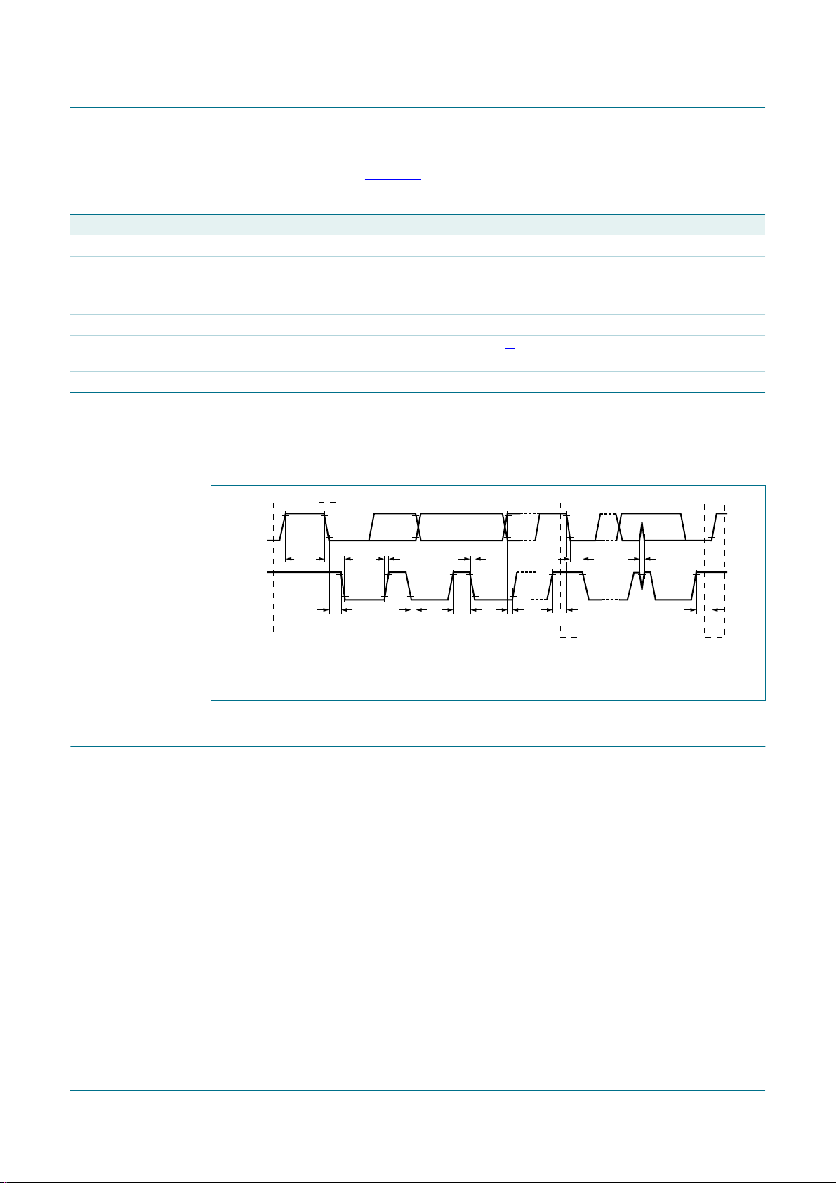
NXP Semiconductors
TFA9812
BTL stereo Class-D audio amplifier with I2S input
Table 57. Characteristics I
V
DDD(3V3)=VDDA(3V3)
= 2.7 V to 3.6 V; V
2
C bus interface; see Figure 10
DDA=VDDP
= 8 V to 20 V;T
…continued
=−20°C to +85°C; all voltages referenced to ground;
amb
unless otherwise specified.
Symbol Parameter Conditions Min Typ Max Unit
t
SU;STO
t
BUF
set-up time for STOP condition 0.6 - - µs
busfree timebetween a STOPand
1.3 - - µs
START condition
t
SU;DAT
t
HD;DAT
t
SP
data set-up time 100 - - ns
data hold time 0 - - µs
pulse width of spikes that must be
[3]
0 - 50 ns
suppressed by the input filter
C
b
[1] Cb is the total capacitance of one bus line in pF. The maximum capacitive load for each bus line is 400 pF.
[2] After this period, the first clock pulse is generated.
[3] To be suppressed by the input filter.
capacitive load for each bus line - - 400 pF
SDA
t
t
BUF
LOW
t
r
t
f
t
HD;STA
t
SP
SCL
P S Sr P
Fig 10. Timing
14. Application information
14.1 Output power estimation
The output power just before clipping can be estimated using Equation 10:
----------------------------------------------------
PO(0.5%)
Where:
VP = supply voltage (V) (V
RL = load impedance (Ω).
RL2R
=
----------------------------------------------------------------------------------------------
t
HD;STA
R
L
DSonRS
2RL⋅
DDP-VSSP
t
HD;DATtHIGHtSU;DAT
2
δ
⋅⋅
+()⋅+
maxVP
).
t
SU;STA
t
SU;STO
010aaa225
(10)
R
= ‘On’ resistance power switch (Ω).
DSon
RS = Series resistance output inductor (Ω).
TFA9812_2 © NXP B.V. 2009. All rights reserved.
Preliminary data sheet Rev. 02 — 22 January 2009 49 of 66
Page 50

NXP Semiconductors
δ
max
The output power at 10 % THD can be estimated using Equation 11:
TFA9812
BTL stereo Class-D audio amplifier with I2S input
= Maximum duty factor (0.96).
PO(10%) 1.25 PO(0.5%)⋅=
Figure 11 and Figure 12 show the estimated output power at THD = 0.5 % and
THD = 10 % as a function of BTL supply voltage for different load impedances.
30
PO (0.5 %)
(W/channel)
20
10
0
8242012 16
(1) 6 Ω
(2) 8 Ω
(3) 16 Ω
Fig 11. BTL PO (0.5 %) as a function of V
010aaa347
(1)
(2)
(3)
VP (V)
P
45
PO (10 %)
W/channel
30
15
0
8242012 16
(1) 6 Ω
(2) 8 Ω
(3) 16 Ω
(1)
(2)
(3)
Fig 12. BTL PO (10 %) as a function of V
010aaa348
(V)
V
P
P
(11)
14.2 Output current limiting
The peak output current is internally limited above a level of 3 A minimum. During normal
operation the output current should not exceed this threshold level of 3 A otherwise the
output signal will be distorted. The peak output current in BTL can be estimated using
Equation 12:
V
I
O max()
≤
-----------------------------------------------------
RL2+ R
P
+〈〉⋅
DSonRS
Where:
VP= supply voltage (V) (V
DDP-VSSP
)
RL= load impedance (Ω)
R
= 'On' resistance power switch (Ω)
DSon
RS= series resistance output inductor (Ω)
TFA9812_2 © NXP B.V. 2009. All rights reserved.
Preliminary data sheet Rev. 02 — 22 January 2009 50 of 66
(12)
Page 51

NXP Semiconductors
Remark: A 4.8 Ω speaker (6 Ω speaker with 20 % spread) in BTL configuration can be
used up to a supply voltage of 17 V without running into current limiting. Current limiting
(clipping) will avoid audio holes, but it causes a distortion comparable to voltage clipping.
14.3 Speaker configuration and impedance
For a flat-frequency response (second-order Butterworth filter) it is necessary to change
the low pass filter components LLC and CLC according to the speaker configuration and
impedance.
Table 58. Filter component values
Impedance (Ω) LLC (µH) CLC (nF)
6 15 680
8 18 560
16 47 330
14.4 Typical application schematics
TFA9812
BTL stereo Class-D audio amplifier with I2S input
TFA9812_2 © NXP B.V. 2009. All rights reserved.
Preliminary data sheet Rev. 02 — 22 January 2009 51 of 66
Page 52

TFA9812_2 © NXP B.V. 2009. All rights reserved.
Preliminary data sheet Rev. 02 — 22 January 2009 52 of 66
xxxxxxxxxxxxxxxxxxxxx xxxxxxxxxxxxxxxxxxxxxxxxxx xxxxxxx x x x xxxxxxxxxxxxxxxxxxxxxxxxxxxxxx xxxxxxxxxxxxxxxxxxx xx xx
xxxxx xxxxxxxxxxxxxxxxxxxxxxxxxxx xxxxxxxxxxxxxxxxxxx xxxxxx xxxxxxxxxxxxxxxxxxxxxxxxxxxxxxxxxxx xxxxxxxxxxxx x x
xxxxxxxxxxxxxxxxxxxxx xxxxxxxxxxxxxxxxxxxxxxxxxxxxxx xxxxx xxxxxxxxxxxxxxxxxxxxxxxxxxxxxxxxxxxxxxxxxxxxxxxxxx xxxxxxxx
xxxxxxxxxxxxxxxxxxxxxxxxx xxxxxxxxxxxxxxxxxxxx xxx
14.4.1 I2S slave mode and Legacy control mode
NXP Semiconductors
DIAGNOSTIC
POWERUP
DC-VOLUME CONTROL
ENABLE
V
DDD
C
vddd
100 nF
I2S DATA
2
I
S WS
2
I
S BCK
2
S MLCK (optional)
I
C
STABD
1 µF
37
ADSEL1/PLIM1
38
SCL/SFOR
39
SDA/MS
40
V
DDD(3V3)
41
STABD
42
REFD
43
TEST2
44
DATA
45
WS
46
BCK
47
MCLK
48
V
SS2
EXPOSED DIE PADDLE
C
DELAY
1 nF
35 34 33 32 31 30 29 28 27 26 25
36
CSEL
ENABLE
24 dB GAIN
AVOL
DIAG
CDELAY
POWERUP
ADSEL2/PLIM2
TFA9812
C
STAB
100 nF
STAB1
SSP1VSSP1
V
BOOT1N
OUT1N
OUT1N
BOOT2P
OUT2P
OUT2P
V
DDP
V
DDP
OUT1P
OUT1P
BOOT1P
OUT2N
OUT2N
R
POWER IN
C
BOOT
15 nF
VP = 8 V to 20 V
GND
VDDA
10 Ω
C
VDDP
220 µF / 25 V
VPA
VP
24
C
VP
C
15 nF
470 pF
470 pF
C
15 nF
BOOT
15 nF
BOOT
C
C
BOOT
SN
SN
RSN 10 Ω
RSN 10 Ω
C
VDDP
100 nF
C
VDDP
100 nF
RSN 10 Ω
RSN 10 Ω
C
SN
470 pF
C
SN
470 pF
Lic
S1 F1
15 µH
Lic
F2 S2
15 µH
S2F2
C
LC
680 nF
C
LC
680 nF
−
+
OUT1
6 Ω to 8 Ω
BTL stereo Class-D audio amplifier with I
C
LC
680 nF
F1S1
C
LC
680 nF
+
−
OUT2
6 Ω to 8 Ω
23
22
21
20
19
18
17
16
15
14
13
XTALIN
XTALOUT
DDA(3V3)
V
STABA
DDA
REFA
V
TEST1
V
SS1
STAB2
SSP2VSSP2
V
12 3 4 56 789 101112
3.3 V VP A
R
STABA
C
VDDA
100 nF
1 kΩ
C
STAB
100 nF
C
VPA
100 nF
C
STAB
100 nF
Fig 13. Simplified application diagram for I2S slave mode and Legacy control mode
BOOT2N
010aaa476
TFA9812
2
S input
Page 53

TFA9812_2 © NXP B.V. 2009. All rights reserved.
Preliminary data sheet Rev. 02 — 22 January 2009 53 of 66
xxxxxxxxxxxxxxxxxxxxx xxxxxxxxxxxxxxxxxxxxxxxxxx xxxxxxx x x x xxxxxxxxxxxxxxxxxxxxxxxxxxxxxx xxxxxxxxxxxxxxxxxxx xx xx
xxxxx xxxxxxxxxxxxxxxxxxxxxxxxxxx xxxxxxxxxxxxxxxxxxx xxxxxx xxxxxxxxxxxxxxxxxxxxxxxxxxxxxxxxxxx xxxxxxxxxxxx x x
xxxxxxxxxxxxxxxxxxxxx xxxxxxxxxxxxxxxxxxxxxxxxxxxxxx xxxxx xxxxxxxxxxxxxxxxxxxxxxxxxxxxxxxxxxxxxxxxxxxxxxxxxx xxxxxxxx
xxxxxxxxxxxxxxxxxxxxxxxxx xxxxxxxxxxxxxxxxxxxx xxx
14.4.2 I2S slave mode and I2C control mode
NXP Semiconductors
DIAGNOSTIC
POWERUP
ENABLE
I2C SCL
2
C SDA
I
VDDD
2
S DATA
I
2
I
S WS
2
I
S BCK
2
S MLCK
I
C
VDDD
100 nF
C
STABD
1 µF
37
ADSEL1/PLIM1
38
SCL/SFOR
39
SDA/MS
40
V
DDD(3V3)
41
STABD
42
REFD
43
TEST2
44
DATA
45
WS
46
BCK
47
MCLK
48
V
SS2
EXPOSED DIE PADDLE
3.3 V
35 34 33 32 31 30 29 28 27 26 25
36
GAIN
CSEL
ENABLE
C
DELAY
AVOL
1 nF
POWERUP
C
STAB
100 nF
DIAG
CDELAY
ADSEL2/PLIM2
TFA9812
STAB1
SSP1VSSP1
V
BOOT1N
BOOT2P
BOOT1P
POWER IN
OUT1N
OUT1N
OUT2P
OUT2P
V
DDP
V
DDP
OUT1P
OUT1P
OUT2N
OUT2N
VP = 8 V to 20 V
24
23
22
21
20
19
18
17
16
15
14
13
C
BOOT
15 nF
VP
C
BOOT
15 nF
C
BOOT
15 nF
C
470 pF
C
470 pF
C
BOOT
15 nF
SN
SN
C
100 nF
C
100 nF
GND
RSN 10 Ω
C
470 pF
C
470 pF
RSN 10 Ω
VDDP
VDDP
RSN 10 Ω
RSN 10 Ω
SN
SN
R
VDDA
10 Ω
C
VDDP
220 µF / 25 V
Lic
S1 F1
15 µH
Lic
F2 S2
15 µH
VPA
VP
S2F2
C
LC
680 nF
C
LC
680 nF
−
+
OUT1
6 Ω to 8 Ω
BTL stereo Class-D audio amplifier with I
C
LC
680 nF
F1S1
C
LC
680 nF
+
−
OUT2
6 Ω to 8 Ω
XTALIN
XTALOUT
DDA(3V3)
V
STABA
DDA
REFA
V
TEST1
V
SS1
STAB2
1 2 3 4 5 6 7 8 9 10 11 12
3.3 V VPA
R
C
VDDA
100 nF
STABA
1 kΩ
C
STAB
100 nF
C
VPA
100 nF
C
STAB
100 nF
Fig 14. Simplified application diagram for I2S slave mode and I2C control mode
SSP2VSSP2
V
BOOT2N
010aaa477
TFA9812
2
S input
Page 54
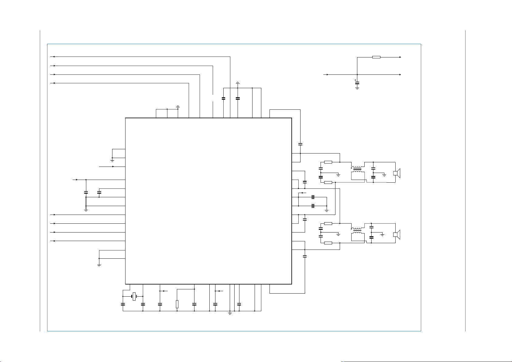
TFA9812_2 © NXP B.V. 2009. All rights reserved.
Preliminary data sheet Rev. 02 — 22 January 2009 54 of 66
xxxxxxxxxxxxxxxxxxxxx xxxxxxxxxxxxxxxxxxxxxxxxxx xxxxxxx x x x xxxxxxxxxxxxxxxxxxxxxxxxxxxxxx xxxxxxxxxxxxxxxxxxx xx xx
xxxxx xxxxxxxxxxxxxxxxxxxxxxxxxxx xxxxxxxxxxxxxxxxxxx xxxxxx xxxxxxxxxxxxxxxxxxxxxxxxxxxxxxxxxxx xxxxxxxxxxxx x x
xxxxxxxxxxxxxxxxxxxxx xxxxxxxxxxxxxxxxxxxxxxxxxxxxxx xxxxx xxxxxxxxxxxxxxxxxxxxxxxxxxxxxxxxxxxxxxxxxxxxxxxxxx xxxxxxxx
xxxxxxxxxxxxxxxxxxxxxxxxx xxxxxxxxxxxxxxxxxxxx xxx
14.4.3 I2S master mode and Legacy control mode
NXP Semiconductors
DIAGNOSTIC
POWERUP
DC-VOLUME CONTROL
ENABLE
V
DDD
C
vddd
100 nF
I2S DATA
2
I
S WS
2
I
S BCK
2
S MLCK (optional)
I
3.3 V
C
STABD
1 µF
37
ADSEL1/PLIM1
38
SCL/SFOR
39
SDA/MS
40
V
DDD(3V3)
41
STABD
42
REFD
43
TEST2
44
DATA
45
WS
46
BCK
47
MCLK
48
V
SS2
EXPOSED DIE PADDLE
C
DELAY
1 nF
35 34 33 32 31 30 29 28 27 26 25
36
CSEL
ENABLE
24 dB GAIN
AVOL
DIAG
STAB1
CDELAY
POWERUP
ADSEL2/PLIM2
TFA9812
C
STAB
100 nF
SSP1VSSP1
V
BOOT1N
OUT1N
OUT1N
BOOT2P
OUT2P
OUT2P
V
DDP
V
DDP
OUT1P
OUT1P
BOOT1P
OUT2N
OUT2N
R
POWER IN
C
BOOT
15 nF
VP = 8 V to 20 V
GND
VDDA
10 Ω
C
VDDP
220 µF / 25 V
VPA
VP
24
VP
C
BOOT
15 nF
C
BOOT
15 nF
470 pF
470 pF
C
BOOT
15 nF
RSN 10 Ω
C
SN
470 pF
C
SN
470 pF
RSN 10 Ω
C
VDDP
100 nF
C
VDDP
100 nF
RSN 10 Ω
C
SN
C
SN
RSN 10 Ω
Lic
S1 F1
15 µH
Lic
F2 S2
15 µH
S2F2
C
LC
680 nF
C
LC
680 nF
−
+
OUT1
6 Ω to 8 Ω
BTL stereo Class-D audio amplifier with I
C
LC
680 nF
F1S1
C
LC
680 nF
+
−
OUT2
6 Ω to 8 Ω
23
22
21
20
19
18
17
16
15
14
13
XTALOUT
C
XTALL
18 pF
DDA(3V3)
V
STABA
3.3 V VP A
R
C
VDDA
100 nF
STABA
1 kΩ
C
100 nF
XTALIN
12 3 4 56 789 101112
XTALL
C
XTALL
18 pF
STAB
DDA
REFA
V
C
VPA
100 nF
SS1
TEST1
V
STAB2
C
STAB
100 nF
SSP2VSSP2
V
Fig 15. Simplified application diagram for I2S master mode and Legacy control mode
BOOT2N
010aaa478
TFA9812
2
S input
Page 55

TFA9812_2 © NXP B.V. 2009. All rights reserved.
Preliminary data sheet Rev. 02 — 22 January 2009 55 of 66
xxxxxxxxxxxxxxxxxxxxx xxxxxxxxxxxxxxxxxxxxxxxxxx xxxxxxx x x x xxxxxxxxxxxxxxxxxxxxxxxxxxxxxx xxxxxxxxxxxxxxxxxxx xx xx
xxxxx xxxxxxxxxxxxxxxxxxxxxxxxxxx xxxxxxxxxxxxxxxxxxx xxxxxx xxxxxxxxxxxxxxxxxxxxxxxxxxxxxxxxxxx xxxxxxxxxxxx x x
xxxxxxxxxxxxxxxxxxxxx xxxxxxxxxxxxxxxxxxxxxxxxxxxxxx xxxxx xxxxxxxxxxxxxxxxxxxxxxxxxxxxxxxxxxxxxxxxxxxxxxxxxx xxxxxxxx
xxxxxxxxxxxxxxxxxxxxxxxxx xxxxxxxxxxxxxxxxxxxx xxx
14.4.4 I2S master mode and I2C control mode
NXP Semiconductors
DIAGNOSTIC
POWERUP
ENABLE
I2C SCL
2
C SDA
I
VDDD
2
S DATA
I
2
I
S WS
2
I
S BCK
2
S MLCK
I
C
VDDD
100 nF
C
STABD
1 µF
37
ADSEL1/PLIM1
38
SCL/SFOR
39
SDA/MS
40
V
DDD(3V3)
41
STABD
42
REFD
43
TEST2
44
DATA
45
WS
46
BCK
47
MCLK
48
V
SS2
EXPOSED DIE PADDLE
3.3 V
35 34 33 32 31 30 29 28 27 26 25
36
GAIN
CSEL
ENABLE
C
DELAY
1 nF
AVOL
DIAG
CDELAY
POWERUP
ADSEL2/PLIM2
TFA9812
C
STAB
100 nF
STAB1
SSP1VSSP1
V
BOOT1N
BOOT2P
BOOT1P
POWER IN
OUT1N
OUT1N
OUT2P
OUT2P
V
DDP
V
DDP
OUT1P
OUT1P
OUT2N
OUT2N
VP = 8 V to 20 V
24
23
22
21
20
19
18
17
16
15
14
13
C
BOOT
15 nF
VP
C
BOOT
15nF
C
BOOT
105 nF
C
470 pF
C
470 pF
C
BOOT
15 nF
SN
SN
C
100 nF
C
100 nF
GND
RSN 10 Ω
C
470 pF
C
470 pF
RSN 10 Ω
VDDP
VDDP
RSN 10 Ω
RSN 10 Ω
SN
SN
R
VDDA
10 Ω
C
VDDP
220 µF / 25 V
Lic
S1 F1
15 µH
Lic
F2 S2
15 µH
VPA
VP
S2F2
C
LC
680 nF
C
LC
680 nF
−
+
OUT1
6 Ω to 8 Ω
BTL stereo Class-D audio amplifier with I
C
LC
680 nF
F1S1
C
LC
680 nF
+
−
OUT2
6 Ω to 8 Ω
XTALIN
12 3 456789101112
XTALL
C
XTALL
18 pF
DDA(3V3)
XTALOUT
V
3.3 V VP A
R
C
XTALL
18 pF
C
100 nF
VDDA
1 kΩ
STABA
STABA
C
STAB
100 nF
DDA
REFA
V
C
VPA
100 nF
TEST1
V
SS1
STAB2
C
100 nF
V
STAB
Fig 16. Simplified application diagram for I2S master mode and I2C control mode
SSP2VSSP2
BOOT2N
010aaa479
TFA9812
2
S input
Page 56
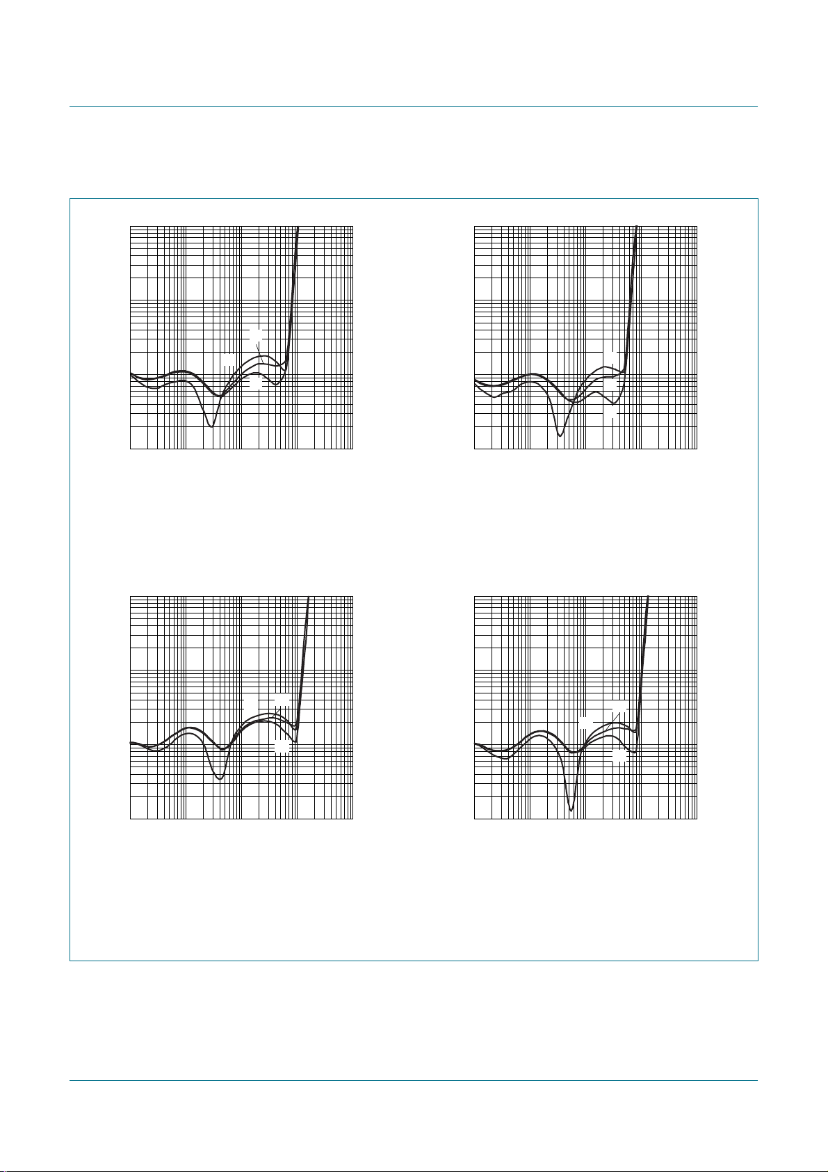
NXP Semiconductors
14.5 Curves measured in typical application
TFA9812
BTL stereo Class-D audio amplifier with I2S input
10
THD+N
(%)
1
−1
10
−2
10
−2
10
(1) fi = 6 kHz
(2) fi = 1 kHz
(3) fi = 100 Hz
(2)
(1)
(3)
−1
1
010aaa480
1010
Po (W/channel)
10
THD+N
(%)
1
−1
10
−2
2
10
10
−2
10
−1
(1) fi = 6 kHz
(2) fi = 1 kHz
(3) fi = 100 Hz
a. VP = 12 V; RL = 2 × 6 Ω b. VP = 12 V; RL = 2 × 8 Ω
10
010aaa482
10
010aaa481
(1)
(2)
(3)
2
1
1010
Po (W/channel)
10
010aaa483
THD+N
(%)
1
−1
10
−2
10
−2
10
(1) fi = 6 kHz
(2) fi = 1 kHz
(3) fi = 100 Hz
(2)
(1)
(3)
−1
1
1010
Po (W/channel)
2
10
THD+N
(%)
1
−1
10
−2
10
−2
10
(1) fi = 6 kHz
(2) fi = 1 kHz
(3) fi = 100 Hz
c. VP = 15 V; RL = 2 × 6 Ω d. VP = 15 V; RL = 2 × 8 Ω
Fig 17. Total harmonic distortion-plus-noise as a function of output power
(2)
(1)
(3)
−1
1
1010
Po (W/channel)
2
10
TFA9812_2 © NXP B.V. 2009. All rights reserved.
Preliminary data sheet Rev. 02 — 22 January 2009 56 of 66
Page 57

NXP Semiconductors
TFA9812
BTL stereo Class-D audio amplifier with I2S input
10
010aaa484
4
f (Hz)
10
THD+N
(%)
1
−1
10
−2
5
10
10 10
2
10
3
10
10
THD+N
(%)
1
−1
10
−2
10
10 10
2
10
3
10
a. VP = 12 V; RL = 2 × 6 Ω; Po = 1 W b. VP = 12 V; RL = 2 × 8 Ω; Po = 1 W
Fig 18. Total harmonic distortion-plus-noise as a function of frequency
3
G
(dB)
010aaa486
0
G
(dB)
−20
10
010aaa485
4
f (Hz)
010aaa487
5
1
(2)
−1
−3
10 10
2
10
3
10
4
10
VP = 12 V; PO = 1 W
(1) RL = 6 Ω 15 µH / 680 µF
(2) RL = 8 Ω 15 µH / 680 µF
(1)
5
f (Hz)
−40
−60
−80
−100
−120
03210.5 1.5 2.5
VP = 12 V; RL = 8 Ω; fi = 1 kHz
(1) 0 dB
(2) 24 dB gain boost
(1)(2)
Fig 19. Gain as a function of frequency Fig 20. Gain as a function of AVOL
AVOL (V)
TFA9812_2 © NXP B.V. 2009. All rights reserved.
Preliminary data sheet Rev. 02 — 22 January 2009 57 of 66
Page 58

NXP Semiconductors
TFA9812
BTL stereo Class-D audio amplifier with I2S input
0
SVRR
(dB)
−20
−40
−60
−80
−100
10 10
VP = 12 V; V
2
10
ripple
3
10
= 500 mV (RMS) reference to ground;
No input signal
(1) RL = 8 Ω
(1)
(2)
10
010aaa488
4
(Hz)
f
i
100
S/N
(dB)
90
80
70
60
5
50
−2
10
−1
(1)
(2)
1
VP = 15 V; 20 kHz AES17 filter
(1) RL = 2 × 8 Ω
(2) RL = 2 × 6 Ω
010aaa489
1010
(W/channel)
P
o
10
(2) RL = 6 Ω
Fig 21. SVRR as a function of frequency Fig 22. S/N ratio as a function of output power
2
25
P
o
(W/chan.)
20
15
10
5
0
0 600480240 360120
(1)
(2)
(3)
010aaa490
time (s)
25
P
o
(W/chan.)
20
15
10
5
0
0 600480240 360120
(1)
(2)
(3)
a. VP = 15 V; RL = 2 × 6 Ω BTL; fi = 1 kHz b. VP = 20 V; RL = 2 × 8 Ω BTL; fi = 1 kHz
(1) T
(2) T
(3) T
act(th_fold)
act(th_fold)
act(th_fold)
= 125 °C
= 105 °C
= 90 °C
Fig 23. Output power as a function of time
010aaa491
time (s)
TFA9812_2 © NXP B.V. 2009. All rights reserved.
Preliminary data sheet Rev. 02 — 22 January 2009 58 of 66
Page 59
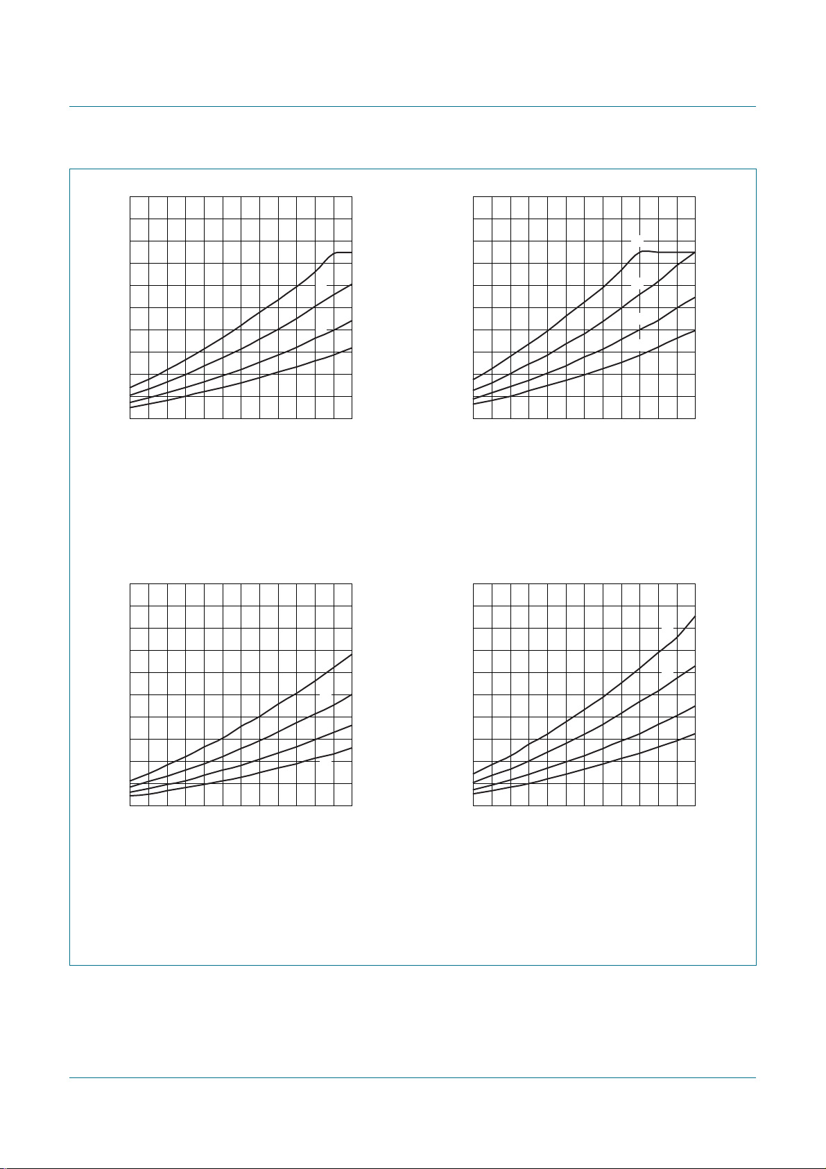
NXP Semiconductors
TFA9812
BTL stereo Class-D audio amplifier with I2S input
25
P
o
(W/chan.)
20
15
10
5
0
82016 1812 1410
(1) Power limiter = 0 dB
(2) Power limiter = −1.5 dB
(3) Power limiter = −3 dB
(4) Power limiter = −4.5 dB
010aaa492
(1)
(2)
(3)
(4)
VP (V)
25
P
o
(W/chan.)
20
15
10
5
0
8201816141210
(1) Power limiter = 0 dB
(2) Power limiter = −1.5 dB
(3) Power limiter = −3 dB
(4) Power limiter = −4.5 dB
010aaa493
(1)
(2)
(3)
(4)
VP (V)
a. VP = 12 V; RL = 2 × 6 Ω; fi = 1 kHz; THD = 1 % b. VP = 12 V; RL = 2 × 6 Ω; fi = 1 kHz; THD = 10 %
25
P
o
(W/chan.)
20
010aaa494
25
P
o
(W/chan.)
20
010aaa495
(1)
(1)
15
10
5
0
820161210 14 18
(1) Power limiter = 0 dB
(2) Power limiter = −1.5 dB
(3) Power limiter = −3 dB
(4) Power limiter = −4.5 dB
(2)
(3)
(4)
VP (V)
15
10
5
0
820161210 14 18
(1) Power limiter = 0 dB
(2) Power limiter = −1.5 dB
(3) Power limiter = −3 dB
(4) Power limiter = −4.5 dB
c. VP = 15 V; RL = 2 × 8 Ω; fi = 1 kHz; THD = 1 % d. VP = 15 V; RL = 2 × 8 Ω; fi = 1 kHz; THD = 10 %
Fig 24. Output power as a function of supply voltage
(2)
(3)
(4)
VP (V)
TFA9812_2 © NXP B.V. 2009. All rights reserved.
Preliminary data sheet Rev. 02 — 22 January 2009 59 of 66
Page 60

NXP Semiconductors
TFA9812
BTL stereo Class-D audio amplifier with I2S input
010aaa496
1010
P
(W/channel)
o
2
10
P
(W)
3
2
(1) (2)
1
0
−2
10
−1
1
VP = 12 V; fi = 1 kHz; Power dissipation in junction only
(1) RL = 2 × 6 Ω
(2) RL = 2 × 8 Ω
Fig 25. Power dissipation as a function of output
power
010aaa497
Po (W/channel)
η
(%)
100
PO
80
60
40
20
0
0108462
(2)
(1)
VP = 12 V; fi = 1 kHz; ηpo = (2 × Po) / (2 × Po + Pd)
(1) RL = 2 × 6 Ω
(2) RL = 2 × 8 Ω
Fig 26. Efficiency as a function of output power
0
α
cs
(dB)
−20
−40
−60
−80
−100
10 10
2
10
VP = 12 V; PO = 1 W
(1) RL = 2 × 6 Ω
(2) RL = 2 × 8 Ω
Fig 27. Channel separation as a function of frequency
010aaa498
(1)
(2)
3
10
4
10
f (Hz)
5
TFA9812_2 © NXP B.V. 2009. All rights reserved.
Preliminary data sheet Rev. 02 — 22 January 2009 60 of 66
Page 61
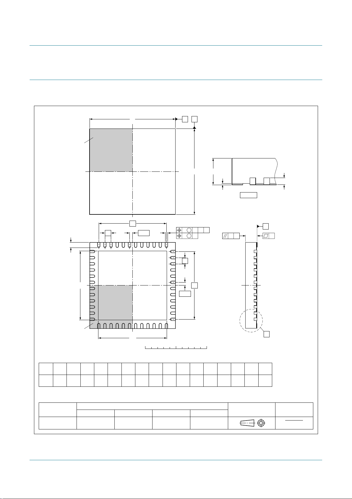
NXP Semiconductors
BTL stereo Class-D audio amplifier with I2S input
15. Package outline
HVQFN48: plastic thermal enhanced very thin quad flat package; no leads;
48 terminals; body 7 x 7 x 0.85 mm
TFA9812
SOT619-8
terminal 1
index area
L
E
D
e
1
e
13 24
12
h
1/2 e
B A
E
M
25
v
e
1/2 e
M
Cw
e
b
A
A
1
detail X
B
AC
2
y
C
1
C
c
y
1
terminal 1
index area
DIMENSIONS (mm are the original dimensions)
(1)
A
UNIT
mm 1
Note
1. Plastic or metal protrusions of 0.075 mm maximum per side are not included.
OUTLINE
VERSION
SOT619-8 - - -
max
A
0.05
0.00
1
48 37
D
h
0 2.5 5 mm
0.2
D
7.1
6.9
(1)
b c
0.30
0.18
IEC JEDEC JEITA
- - -
DhE
5.75
5.45
MO-220
(1)
E
7.1
5.75
6.9
5.45
REFERENCES
h
36
scale
e
e1e
0.5
5.5 5.5 0.1
X
L
0.5
0.3
v w
0.05y0.05
EUROPEAN
PROJECTION
2
y
0.1
1
ISSUE DATE
07-01-10
07-01-30
Fig 28. Package outline SOT619-8 (HVQFN48)
TFA9812_2 © NXP B.V. 2009. All rights reserved.
Preliminary data sheet Rev. 02 — 22 January 2009 61 of 66
Page 62

NXP Semiconductors
16. Handling information
It is advisable to abide by the normal precautions appropriate to handling MOS devices.
TFA9812
BTL stereo Class-D audio amplifier with I2S input
TFA9812_2 © NXP B.V. 2009. All rights reserved.
Preliminary data sheet Rev. 02 — 22 January 2009 62 of 66
Page 63

NXP Semiconductors
BTL stereo Class-D audio amplifier with I2S input
TFA9812
17. Revision history
Table 59. Revision history
Document ID Release date Data sheet status Change notice Supersedes
TFA9812_2 20090122 Preliminary data sheet - TFA9812_1
Modifications:
TFA9812_1 2008/10/30 Preliminary data sheet - -
• Table 55 “DC characteristics” V
maximum value updated.
IH
TFA9812_2 © NXP B.V. 2009. All rights reserved.
Preliminary data sheet Rev. 02 — 22 January 2009 63 of 66
Page 64

NXP Semiconductors
18. Legal information
18.1 Data sheet status
TFA9812
BTL stereo Class-D audio amplifier with I2S input
Document status
Objective [short] data sheet Development This document contains data from the objective specification for product development.
Preliminary [short] data sheet Qualification This document contains data from the preliminary specification.
Product [short] data sheet Production This document contains the product specification.
[1] Please consult the most recently issued document before initiating or completing a design.
[2] The term ‘short data sheet’ is explained in section “Definitions”.
[3] The product status of device(s) described in this document mayhave changed since this document was published and may differ in case of multiple devices.The latest product status
information is available on the Internet at URL
[1][2]
Product status
18.2 Definitions
Draft — The document is a draft version only. The content is still under
internal review and subject to formal approval, which may result in
modifications or additions. NXP Semiconductors does not give any
representations or warranties as to the accuracy or completeness of
information included herein and shall have no liability for the consequences of
use of such information.
Short data sheet — A short data sheet is an extract from a full data sheet
with the same product type number(s) and title. A short data sheet is intended
for quick reference only and should not be relied upon to contain detailed and
full information. For detailed and full information see the relevant full data
sheet, which is available on request via the local NXP Semiconductors sales
office. In case of any inconsistency or conflict with the short data sheet, the
full data sheet shall prevail.
18.3 Disclaimers
General — Information in this document is believed to be accurate and
reliable. However, NXP Semiconductors does not give any representations or
warranties, expressedor implied, as to the accuracy or completeness of such
information and shall have no liability for the consequences of use of such
information.
Right to make changes — NXP Semiconductors reserves the right to make
changes to information published in this document, including without
limitation specifications and product descriptions, at any time and without
notice. This document supersedes and replaces all information supplied prior
to the publication hereof.
Suitability for use — NXP Semiconductors products are not designed,
authorized or warranted to be suitable for use in medical, military, aircraft,
space or life support equipment, nor in applications where failure or
malfunction of an NXP Semiconductors product can reasonably be expected
to result in personal injury, death or severe property or environmental
[3]
http://www.nxp.com.
Definition
damage. NXP Semiconductors accepts no liability for inclusion and/or use of
NXP Semiconductors products in such equipment or applications and
therefore such inclusion and/or use is at the customer’s own risk.
Applications — Applications that are described herein for any of these
products are for illustrative purposes only. NXP Semiconductors makes no
representation or warranty that such applications will be suitable for the
specified use without further testing or modification.
Quick reference data — The Quick reference data is an extract of the
product data given in the Limiting values and Characteristics sections of this
document, and as such is not complete, exhaustive or legally binding.
Limiting values — Stress above one or more limiting values (as defined in
the Absolute Maximum Ratings System of IEC 60134) may cause permanent
damage to the device. Limiting values are stress ratings only and operation of
the device at these or any other conditions above those given in the
Characteristics sections of this document is not implied. Exposure to limiting
values for extended periods may affect device reliability.
Terms and conditions of sale — NXP Semiconductors products are sold
subject to the general terms and conditions of commercial sale, as published
at
http://www.nxp.com/profile/terms, including those pertaining to warranty,
intellectual property rights infringement and limitation of liability, unless
explicitly otherwise agreed to in writing by NXP Semiconductors. In case of
any inconsistency or conflict between information in this document and such
terms and conditions, the latter will prevail.
No offer to sell or license — Nothing in this document may be interpreted
or construed as an offer to sell products that is open for acceptance or the
grant, conveyanceor implication of any license under any copyrights, patents
or other industrial or intellectual property rights.
18.4 Trademarks
Notice: All referenced brands,product names,service names and trademarks
are the property of their respective owners.
I2C-bus — logo is a trademark of NXP B.V.
19. Contact information
For more information, please visit: http://www.nxp.com
For sales office addresses, please send an email to: salesaddresses@nxp.com
TFA9812_2 © NXP B.V. 2009. All rights reserved.
Preliminary data sheet Rev. 02 — 22 January 2009 64 of 66
Page 65

NXP Semiconductors
20. Contents
TFA9812
BTL stereo Class-D audio amplifier with I2S input
1 General description. . . . . . . . . . . . . . . . . . . . . . 1
2 Features . . . . . . . . . . . . . . . . . . . . . . . . . . . . . . . 1
2.1 General features. . . . . . . . . . . . . . . . . . . . . . . . 1
2.2 DSP features . . . . . . . . . . . . . . . . . . . . . . . . . . 2
2.3 Audio data input interface format support. . . . . 2
3 Applications. . . . . . . . . . . . . . . . . . . . . . . . . . . . 2
4 Quick reference data . . . . . . . . . . . . . . . . . . . . . 3
5 Ordering information. . . . . . . . . . . . . . . . . . . . . 4
6 Block diagram . . . . . . . . . . . . . . . . . . . . . . . . . . 5
7 Pinning information. . . . . . . . . . . . . . . . . . . . . . 6
7.1 Pinning . . . . . . . . . . . . . . . . . . . . . . . . . . . . . . . 6
8 Functional description . . . . . . . . . . . . . . . . . . . 8
8.1 General. . . . . . . . . . . . . . . . . . . . . . . . . . . . . . . 8
8.2 Functional modes . . . . . . . . . . . . . . . . . . . . . . . 9
8.2.1 Control modes . . . . . . . . . . . . . . . . . . . . . . . . . 9
8.2.2 Key operating modes . . . . . . . . . . . . . . . . . . . . 9
8.2.3 I
2
S master/slave modes and MCLK/BCK
clock modes . . . . . . . . . . . . . . . . . . . . . . . . . . 10
8.3 Power-up/power-down . . . . . . . . . . . . . . . . . . 13
8.3.1 Power-up . . . . . . . . . . . . . . . . . . . . . . . . . . . . 13
8.3.2 Power-down . . . . . . . . . . . . . . . . . . . . . . . . . . 14
8.4 Digital audio data input. . . . . . . . . . . . . . . . . . 14
8.4.1 Digital audio data format support . . . . . . . . . . 14
8.4.2 Digital audio data format control. . . . . . . . . . . 16
8.5 Digital signal-processing features. . . . . . . . . . 16
8.5.1 Equalizer. . . . . . . . . . . . . . . . . . . . . . . . . . . . . 16
8.5.1.1 Equalizer options . . . . . . . . . . . . . . . . . . . . . . 16
8.5.1.2 Equalizer band function . . . . . . . . . . . . . . . . . 16
8.5.1.3 Equalizer band control . . . . . . . . . . . . . . . . . . 18
8.5.2 Digital volume control . . . . . . . . . . . . . . . . . . . 20
8.5.3 Soft mute and mute . . . . . . . . . . . . . . . . . . . . 21
8.5.4 Output signal and word-select polarity control 21
8.5.5 Gain boost and clip level control. . . . . . . . . . . 21
8.5.6 Output power limiter . . . . . . . . . . . . . . . . . . . . 22
8.5.7 PWM control for performance improvement. . 22
8.6 Class-D amplification . . . . . . . . . . . . . . . . . . . 23
8.7 Protection mechanisms . . . . . . . . . . . . . . . . . 23
8.7.1 Thermal foldback . . . . . . . . . . . . . . . . . . . . . . 24
8.7.2 Overtemperature protection . . . . . . . . . . . . . . 24
8.7.3 Overcurrent protection . . . . . . . . . . . . . . . . . . 24
8.7.4 Overvoltage protection . . . . . . . . . . . . . . . . . . 24
8.7.5 Undervoltage protections . . . . . . . . . . . . . . . . 24
8.7.6 Overdissipation protection . . . . . . . . . . . . . . . 25
8.7.7 Window protection . . . . . . . . . . . . . . . . . . . . . 25
8.7.8 Lock protection . . . . . . . . . . . . . . . . . . . . . . . . 25
8.7.9 Underfrequency protection . . . . . . . . . . . . . . . 25
8.7.10 Overfrequency protection. . . . . . . . . . . . . . . . 25
8.7.11 Invalid BCK protection . . . . . . . . . . . . . . . . . . 26
8.7.12 DC blocking . . . . . . . . . . . . . . . . . . . . . . . . . . 26
8.7.13 Overview protections . . . . . . . . . . . . . . . . . . . 26
9I
9.1 I
9.2 I
9.3 I
9.4 I
2
C bus interface and register settings . . . . . 27
2
C bus interface. . . . . . . . . . . . . . . . . . . . . . . 27
2
C bus TFA9812 device addresses. . . . . . . . 27
2
C write cycle description . . . . . . . . . . . . . . . 28
2
C read cycle description . . . . . . . . . . . . . . . 28
9.5 Top-level register map . . . . . . . . . . . . . . . . . . 29
9.5.1 Interpolator settings and soft mute. . . . . . . . . 31
9.5.2 Volume control . . . . . . . . . . . . . . . . . . . . . . . . 31
9.5.3 Digital input format . . . . . . . . . . . . . . . . . . . . . 32
9.5.4 Equalizer configuration. . . . . . . . . . . . . . . . . . 32
9.5.5 Equalizer settings. . . . . . . . . . . . . . . . . . . . . . 33
9.5.6 PWM signal control . . . . . . . . . . . . . . . . . . . . 35
9.5.7 Digital-in clock configuration. . . . . . . . . . . . . . 36
9.5.8 Thermal foldback control . . . . . . . . . . . . . . . . 36
9.5.9 TFA9812 temperature . . . . . . . . . . . . . . . . . . 37
9.5.10 Miscellaneous status . . . . . . . . . . . . . . . . . . . 37
9.6 Overview of functional control in each
control mode . . . . . . . . . . . . . . . . . . . . . . . . . 38
10 Internal circuitry . . . . . . . . . . . . . . . . . . . . . . . 39
11 Limiting values . . . . . . . . . . . . . . . . . . . . . . . . 42
12 Thermal characteristics . . . . . . . . . . . . . . . . . 43
13 Characteristics . . . . . . . . . . . . . . . . . . . . . . . . 44
13.1 DC Characteristics. . . . . . . . . . . . . . . . . . . . . 44
13.2 AC characteristics . . . . . . . . . . . . . . . . . . . . . 47
13.3 Timing . . . . . . . . . . . . . . . . . . . . . . . . . . . . . . 48
14 Application information . . . . . . . . . . . . . . . . . 49
14.1 Output power estimation . . . . . . . . . . . . . . . . 49
14.2 Output current limiting . . . . . . . . . . . . . . . . . . 50
14.3 Speaker configuration and impedance. . . . . . 51
14.4 Typical application schematics. . . . . . . . . . . . 51
14.4.1 I
14.4.2 I
14.4.3 I
14.4.4 I
2
S slave mode and Legacy control mode . . . 52
2
S slave mode and I2C control mode . . . . . . 53
2
S master mode and Legacy control mode . 54
2
S master mode and I2C control mode . . . . . 55
14.5 Curves measured in typical application . . . . . 56
15 Package outline. . . . . . . . . . . . . . . . . . . . . . . . 61
16 Handling information . . . . . . . . . . . . . . . . . . . 62
17 Revision history . . . . . . . . . . . . . . . . . . . . . . . 63
18 Legal information . . . . . . . . . . . . . . . . . . . . . . 64
18.1 Data sheet status . . . . . . . . . . . . . . . . . . . . . . 64
18.2 Definitions . . . . . . . . . . . . . . . . . . . . . . . . . . . 64
18.3 Disclaimers. . . . . . . . . . . . . . . . . . . . . . . . . . . 64
continued >>
TFA9812_2 © NXP B.V. 2009. All rights reserved.
Preliminary data sheet Rev. 02 — 22 January 2009 65 of 66
Page 66

NXP Semiconductors
18.4 Trademarks. . . . . . . . . . . . . . . . . . . . . . . . . . . 64
19 Contact information. . . . . . . . . . . . . . . . . . . . . 64
20 Contents . . . . . . . . . . . . . . . . . . . . . . . . . . . . . . 65
TFA9812
BTL stereo Class-D audio amplifier with I2S input
Please be aware that important notices concerning this document and the product(s)
described herein, have been included in section ‘Legal information’.
© NXP B.V. 2009. All rights reserved.
For more information, please visit: http://www.nxp.com
For sales office addresses, please send an email to: salesaddresses@nxp.com
Date of release: 22 January 2009
Document identifier: TFA9812_2
 Loading...