

Page 1

TFA9810
Stereo full-bridge audio amplifier 2 x 12 W
Rev. 03 — 20 February 2008 Product data sheet
1. General description
The TFA9810 is a two-channel power comparator for high-efficiency class D audio
amplifier systems. It contains two full-bridge Bridge-Tied Load (BTL) power stages, drive
logic, protection control logic and full differential input comparators. By using this power
comparator a compact closed-loop self-oscillating digital amplifier system or open-loop
system can be built. The TFA9810 does not require a heat sink and operates using an
asymmetrical supply voltage.
2. Features
n Stereo full-bridge power comparator for class D audio amplifier applications
n No external heat sink required
n Operating voltage range: asymmetrical from 8 V to 20 V
n Thermally protected
n Zero dead-time switching
n Current-limiting (no audible interruptions)
3. Applications
n Self-oscillating or open-loop class D audio amplifier applications
n Flat-panel television sets
n Flat-panel monitors
n Multimedia systems
n Wireless speakers
n High-end CRT television sets
4. Quick reference data
Table 1. Quick reference data
T
= 25°C; VP = 12 V; f
amb
Symbol Parameter Condition Min Typ Max Unit
V
P
I
off
I
q
η
po
= 550 kHz; Figure 33 unless otherwise specified
osc
supply voltage VP = V
off-state current off mode - 110 200 µA
quiescent current with load, filter and
snubbers connected
output power
efficiency
output power
2 x 9 W into 8 Ω;
P
o=Po(nom)
DDPx
− V
SSPx
81220V
-3545mA
87 89 - %
Page 2

NXP Semiconductors
TFA9810
Audio amplifier 2 x 12 W
Table 1. Quick reference data
T
= 25°C; VP = 12 V; f
amb
osc
…continued
= 550 kHz; Figure 33 unless otherwise specified
Symbol Parameter Condition Min Typ Max Unit
P
o(RMS)
RMS output power RL = 8 Ω; VP = 12 V;
- 9.5 - W
THD = 10 %;Twochannel
driven; no heat sink
required.
P
o
output power VP = 12 V; RL = 8 Ω ----
THD = 10 % 8.5 9.5 - W
THD = 1 % 6.5 7.5 - W
= 14 V; RL= 8 Ω;
V
P
-15-W
THD = 10 %; thermally
limited
V
= 16 V; RL= 8 Ω;
P
-15-W
THD = 10 %; thermally
limited
V
= 12 V; RL= 6 Ω;
P
-12-W
THD = 10 %; thermally
limited
V
= 12 V; RL = 4 Ω;
P
-15-W
THD = 10 %; thermally
limited
5. Ordering information
Table 2. Ordering information
Type number Package
Name Description Version
TFA9810T SO32 SO32: plastic small outline package; 32 leads; body width 7.5 mm SOT287-1
TFA9810_3 © NXP B.V. 2008. All rights reserved.
Product data sheet Rev. 03 — 20 February 2008 2 of 29
Page 3
NXP Semiconductors
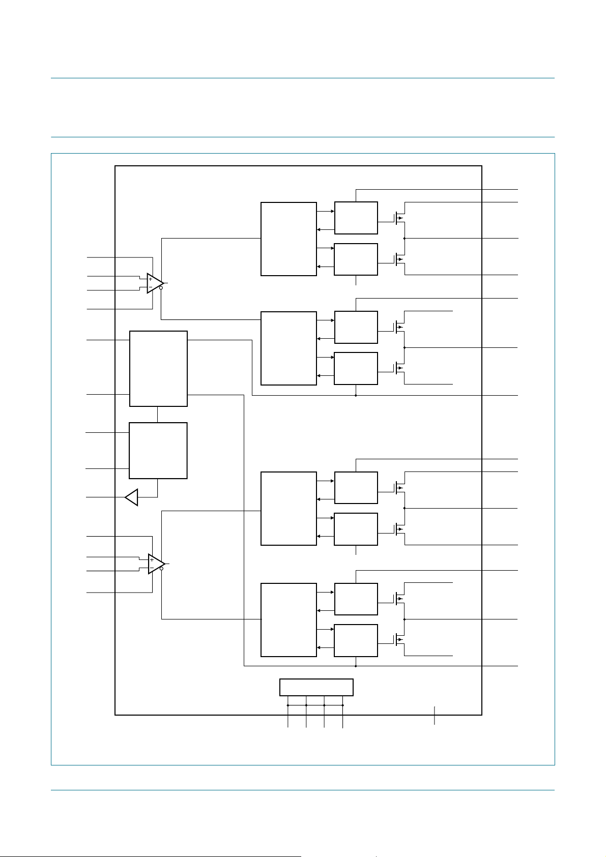
6. Block diagram
TFA9810
Audio amplifier 2 x 12 W
V
DDA1
IN1P
IN1N
V
SSA1
DIAG
TEST
SO/OL
ENABLE
CDELAY
V
DDA2
IN2P
IN2N
V
SSA2
TFA9810
4
2
3
5
10
PROTECTION
11
6
REFERENCE
7
8
13
15
14
12
COMPARATOR 1
OVP
UVP
OCP
OTP
ODP
WP
COMPARATOR 2
CONTROL
LOGIC
CONTROL
LOGIC
CONTROL
LOGIC
CONTROL
LOGIC
DRIVER
HIGH
DRIVER
LOW
STABI1
DRIVER
HIGH
DRIVER
LOW
DRIVER
HIGH
DRIVER
LOW
STABI2
DRIVER
HIGH
DRIVER
LOW
V
V
V
V
DDP1
SSP1
DDP2
SSP2
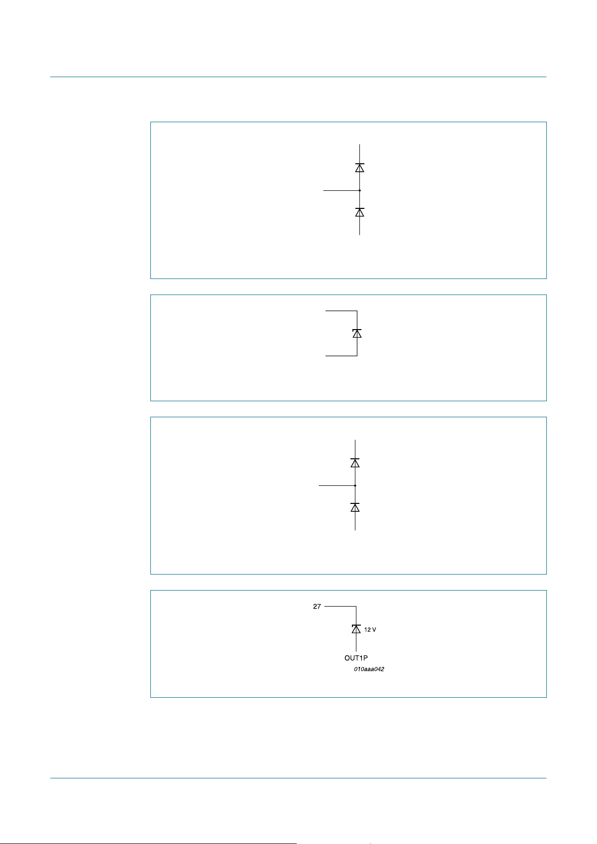
27
25
26
30
29
28
31
22
24
23
19
20
21
18
BOOT1P
V
DDP1
OUT1P
V
SSP1
BOOT1N
OUT1N
STAB1
BOOT2P
V
DDP2
OUT2P
V
SSP2
BOOT2N
OUT2N
STAB2
HEATSPREADER
1161732
V
SSD(HW)
n.c.
9
010aaa016
Fig 1. Block diagram
TFA9810_3 © NXP B.V. 2008. All rights reserved.
Product data sheet Rev. 03 — 20 February 2008 3 of 29
Page 4
NXP Semiconductors
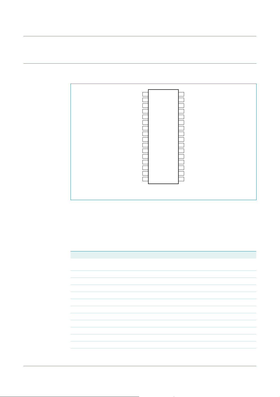
7. Pinning information
7.1 Pinning
TFA9810
Audio amplifier 2 x 12 W
V
SSD(HW)
ENABLE OUT1P
CDELAY V
V
SSD(HW)
1
2
IN1P STAB1
3
IN1N V
4
V
DDA1
5
V
SSA1
6
SO/OL BOOT1P
7
8
TFA9810
9
n.c. V
10
DIAG OUT2P
11
TEST BOOT2P
12
V
SSA2
13
V
DDA2
14
IN2N V
15
IN2P STAB2
16
SO32
010aaa017
32
31
30
29
28
27
26
25
24
23
22
21
20
19
18
17
V
SSD(HW)
SSP1
BOOT1N
OUT1N
DDP1
DDP2
OUT2N
BOOT2N
SSP2
V
SSD(HW
)
Fig 2. Pin configuration
The SO32 package has four corner leads. These leads (1, 16, 17, and 32) are internally
connected to the die pad and must be connected to V
in the application. Together with
SSA
the applied copper area on the Printed Circuit Board (PCB) these leads determine the
ambient temperature, which affects the thermal resistance of the junction.
7.2 Pin description
Table 3. Pin description
Symbol Pin Description
V
SSD(HW)
IN1P 2 Positive input comparator channel 1
IN1N 3 Negative input comparator channel 1
V
DDA1
V
SSA1
SO/OL 6 SO/OL input enables self-oscillating / open-loop configuration
ENABLE 7 Enable input to switch between SLEEP and OPERATING
CDELAY 8 CDELAY input determines the switch on/off timing
n.c. 9 Not connected
DIAG 10 Diagnostic output; open drain
TEST 11 Test signal input; for testing purposes only
V
SSA2
V
DDA2
TFA9810_3 © NXP B.V. 2008. All rights reserved.
Product data sheet Rev. 03 — 20 February 2008 4 of 29
1, 16, 17,32Negative digital supply voltage and handle wafer
4 Positive analog supply voltage channel 1
5 Negative analog supply voltage channel 1
12 Negative analog supply voltage channel 2
13 Positive analog supply voltage channel 2
Page 5

NXP Semiconductors
TFA9810
Audio amplifier 2 x 12 W
Table 3. Pin description
Symbol Pin Description
IN2N 14 Negative input comparator channel 2
IN2P 15 Positive input comparator channel 2
STAB2 18 Decoupling of internal 11 V regulator for channel 2 drivers
V
SSP2
BOOT2N 20 Bootstrap high-side driver negative output channel 2
OUT2N 21 Negative output channel 2
BOOT2P 22 Bootstrap high-side driver positive output channel 2
OUT2P 23 Positive output channel 2
V
DDP2
V
DDP1
OUT1P 26 Positive output channel 1
BOOT1P 27 Bootstrap high-side driver positive output channel 1
OUT1N 28 Negative output channel 1
BOOT1N 29 Bootstrap high-side driver negative output channel 1
V
SSP1
STAB1 31 Decoupling of internal 11 V regulator for channel 1 drivers
8. Functional description
…continued
19 Negative power-supply voltage channel 2
24 Positive supply voltage power channel 2
25 Positive power supply voltage channel 1
30 Negative supply voltage power channel 1
8.1 General
The TFA9810 is a dual-switching power comparator. It is the main building block for a
stereo high-efficiency Class D audio power amplifier system. It contains two full-bridge
BTL power stages, drive logic, protection-control logic and full differential input
comparators and references (see Figure 1). By using this power comparator a compact
closed-loop self-oscillating digital amplifier system or open-loop system can be built. A
second-order low-pass filter converts the Pulse Width Modulation (PWM) output signal
into an analog audio signal across the speaker.
8.2 Interfacing
The pins ENABLE and SO/OL control the operating mode of the TFA9810. Both the
ENABLE and the SO/OL pins refer to V
When the SO/OL pin is connected to V
SSD(HW)
SSA
the SO/OL pin is floating the TFA9810 is in open-loop mode.
The TEST pin needs to be connected to V
Table 4. SO/OL connections
Interfacing
SO/OL connected to Configuration
V
SSD(HW)
Open Open-loop
.
the TFA9810 is in self-oscillating mode: when
in both situations.
DDA
Self-oscillating
The device has two modes: SLEEP and OPERATING.
TFA9810_3 © NXP B.V. 2008. All rights reserved.
Product data sheet Rev. 03 — 20 February 2008 5 of 29
Page 6

NXP Semiconductors
In SLEEP mode the TFA9810 is not biased and has a very low supply current.
When the TFA9810 is set to OPERATING mode the device is started via the start-up
sequence, which provides a pop-free start-up behavior. After start-up the reference
voltages STAB are present and the outputs start switching.
Table 5. Start-up
Interfacing
ENABLE [V] Mode
ENABLE < 0.8 V SLEEP
ENABLE > 3 V OPERATING
8.3 Input comparators
The input stages have a differential input and are optimized for low noise and low offset.
This results in maximum flexibility in the application.
8.3.1 Operating in self-oscillating configuration
The inputs (IN1P,IN1N, IN2P, IN2N) of the comparators are internally set to a voltage level
of 0.5VP, but only during the start-up sequence. In operating mode the inputs are
high-ohmic.
TFA9810
Audio amplifier 2 x 12 W
8.3.2 Operating in open-loop configuration
No internal voltages are applied to the inputs. The input pins (IN1P, IN1N, IN2P, IN2N) are
pulled down to V
level by internal resistors.
SSA
8.4 Diagnostic
The DIAG output is an open-drain output. The maximum current is 2 mA. Whenever one
of the protections is triggered the DIAG output is activated low. The DIAG output refers to
V
.
SSD
8.5 Protections
Overtemperature, overcurrent, overvoltage, undervoltage, overdissipation sensors, and
window protection are included in the TFA9810. When one of these sensors exceeds its
threshold level either the output power stage is switched off and the outputs (OUT1N,
OUT1P, OUT2N, OUT2P) become floating, or the TFA9810 shuts down and starts up
immediately.
• OverTemperature Protection (OTP)
If the junction temperature (Tj) exceeds a threshold level of about 150 °C then the
outputs become floating. The device will start switching again after 5 µs and when the
temperature is below 150 °C. This is thermal limitation without audible interruptions.
• OverCurrent Protection (OCP)
If the output current exceeds the maximum output current threshold level the output
becomes floating. The device will start switching again after 5 µs. This is current
limitation without audible interruptions.
TFA9810_3 © NXP B.V. 2008. All rights reserved.
Product data sheet Rev. 03 — 20 February 2008 6 of 29
Page 7

NXP Semiconductors
• OverVoltage Protection (OVP)
• UnderVoltage Protection (UVP)
• OverDissipation Protection (ODP)
• Window Protection (WP)
TFA9810
Audio amplifier 2 x 12 W
When the supply voltage applied to the TFA9810 exceeds the maximum supply
voltage threshold level the device will shut down. The device will restart when the
supply voltage is within the operating range.
When the supply voltage applied to the TFA9810 falls below the minimum supply
voltage threshold level the device will shut down. The device will restart when the
supply voltage is within the operating range.
The ODP in the TFA9810 is a combination of two protections. Exceeding a
temperature threshold level of 135 °C an internal pre-warning is generated. When an
overcurrent is detected during the pre-warning the device will shut down. When the
ENABLE pin is high the TFA9810 will restart automatically. The restart sequence
(switch-off → switch-on) will take 200 ms to 500 ms.
During start-up, if one of the outputs is shorted to VSSor VDDthe device will not start.
This is an effective measure to protect the device against shorts between the outputs
(beforethe filter) and the groundor supply lines. The supply must be switchedoff prior
to removing any short. The WP protects the device against failure during board
assembly.
Table 6. Overview protections
Protections
Symbol Condition DIAG Outputs Recovering
OTP T
OCP I
OVP VP > 20 V LOW Floating Restart (switch-off → switch-on when VP< 20 V)
UVP V
ODP T
WP OUTX > V
> 150 °C LOW Floating Automatic, after 5 µs and Tj < 150 °C
j
> I
O
ORM
< 8 V LOW Floating Restart (switch-off → switch-on when VP> 8 V)
P
> 135 °C and IO > I
j
- 1 V or
OUTX < V
DDA
SSA
+ 1 V
LOW Floating Automatic, after 5 µs and IO < I
LOW Floating Restart (switch-off → switch-on when
ORM
LOW
T
< 135 °CorIO<I
j
ORM
ORM
)
TFA9810_3 © NXP B.V. 2008. All rights reserved.
Product data sheet Rev. 03 — 20 February 2008 7 of 29
Page 8
NXP Semiconductors
8.6 Start-up sequence
V
P
ENABLE
STAB1
CDELAY
TFA9810
Audio amplifier 2 x 12 W
V IN x
FLOATING
OUT x
AUDIO
DIAG
SLEEP START-UP OPERATING FAULT RESTART OPERATING SHUT-DOWN SLEEP
Fig 3. Start-up sequence
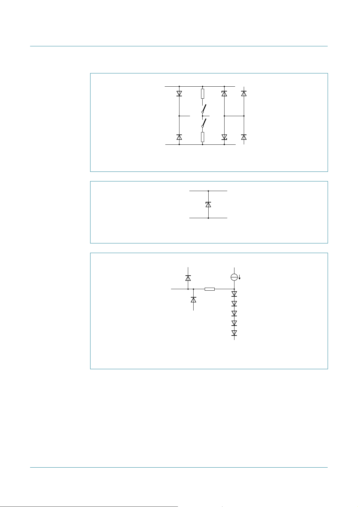
9. Internal circuitry
PWM
AUDIO
1,16, 17, 32
FLOATING
PWM
AUDIO
V
010aaa018
DDA
22 V
V
SSA
010aaa024
Fig 4. Internal circuitry 0001
TFA9810_3 © NXP B.V. 2008. All rights reserved.
Product data sheet Rev. 03 — 20 February 2008 8 of 29
Page 9
NXP Semiconductors
TFA9810
Audio amplifier 2 x 12 W
V
2
135 kΩ
DDA1
5.5 V
3
Fig 5. Internal circuitry 0002
Fig 6. Internal circuitry 0003
V
DDA1
V
135 kΩ
110 kΩ
SSA
22 V
010aaa026
5.5 V
V
DDA1
V
SSA1
010aaa025
50 µA
hvp
4
5
6
V
SSA1
V
SSA
010aaa027
Fig 7. Internal circuitry 0004
TFA9810_3 © NXP B.V. 2008. All rights reserved.
Product data sheet Rev. 03 — 20 February 2008 9 of 29
Page 10

NXP Semiconductors
V
TFA9810
Audio amplifier 2 x 12 W
DDA1
7
Fig 8. Internal circuitry 0005
8
Fig 9. Internal circuitry 0006
V
DDA1
3 kΩ
2 nA
200 nA 5 kΩ
250 nA
V
SSA
010aaa028
DISCHARGE
V
SSA1
010aaa029
V
DDA1
10
V
V
SSA1
SSD
010aaa030
Fig 10. Internal circuitry 0007
TFA9810_3 © NXP B.V. 2008. All rights reserved.
Product data sheet Rev. 03 — 20 February 2008 10 of 29
Page 11

NXP Semiconductors
V
TFA9810
Audio amplifier 2 x 12 W
DDA1
Fig 11. Internal circuitry 0008
Fig 12. Internal circuitry 0009
14
11
130 kΩ
13 kΩ
V
SSA1
010aaa031
V
5.5 V
DDA2
hvp
15
V
130 kΩ
SSA2
5.5 V
V
SSA2
010aaa033
Fig 13. Internal circuitry 0010
V
DDA2
100 mA
18
12 V
V
SSD
010aaa034
Fig 14. Internal circuitry 0011
TFA9810_3 © NXP B.V. 2008. All rights reserved.
Product data sheet Rev. 03 — 20 February 2008 11 of 29
Page 12

NXP Semiconductors
Fig 15. Internal circuitry 0012
Fig 16. Internal circuitry 0013
TFA9810
Audio amplifier 2 x 12 W
24
23.5 V
19
010aaa035
20
12 V
OUT2N
010aaa036
Fig 17. Internal circuitry 0014
Fig 18. Internal circuitry 0015
V
DDP2
21
V
SSP2
010aaa037
22
12 V
OUT2P
010aaa038
TFA9810_3 © NXP B.V. 2008. All rights reserved.
Product data sheet Rev. 03 — 20 February 2008 12 of 29
Page 13
NXP Semiconductors
Fig 19. Internal circuitry 0016
TFA9810
Audio amplifier 2 x 12 W
V
DDP2
23
V
SSP2
010aaa039
25
23.5 V
30
010aaa040
Fig 20. Internal circuitry 0017
Fig 21. Internal circuitry 0018
V
DDP1
26
V
SSP1
010aaa041
Fig 22. Internal circuitry 0019
TFA9810_3 © NXP B.V. 2008. All rights reserved.
Product data sheet Rev. 03 — 20 February 2008 13 of 29
Page 14

NXP Semiconductors
Fig 23. Internal circuitry 0020
TFA9810
Audio amplifier 2 x 12 W
V
DDP1
28
V
SSP1
010aaa043
29
12 V
Fig 24. Internal circuitry 0021
Fig 25. Internal circuitry 0022
10. Limiting values
Table 7. Limiting values
In accordance with the Absolute Maximum Rating System (IEC 60134).
Symbol Parameter Conditions Min Max Unit
V
P
I
ORM
T
j
T
stg
T
amb
P
max
OUT1N
010aaa044
V
DDA1
100 mA
31
12 V
V
SSD
010aaa045
supply voltage asymmetrical −0.3 +23 V
repetitive peak output current 3 - A
junction temperature - +150 °C
storage temperature −55 +150 °C
ambient temperature −40 +85 °C
maximum power dissipation - 2.5 W
TFA9810_3 © NXP B.V. 2008. All rights reserved.
Product data sheet Rev. 03 — 20 February 2008 14 of 29
Page 15

NXP Semiconductors
TFA9810
Audio amplifier 2 x 12 W
Table 7. Limiting values
…continued
In accordance with the Absolute Maximum Rating System (IEC 60134).
Symbol Parameter Conditions Min Max Unit
V
x
voltage on pin x DIAG VSS− 0.3 +12 V
IN1P - IN1N −12 +12 V
IN2P - IN2N −12 +12 V
all other pins V
V
esd
electrostatic discharge voltage VINX with
− 0.3 VDD + 0.3 V
SS
−1500 +1500 V
respect to
other pins
all other pins −2000 +2000 V
11. Thermal characteristics
Table 8. Characteristics
Symbol Parameter Conditions Min Typ Max Unit
[1] [2]
[1]
-
-
[1]
41
44
44
-
K/W
K/W
30 K/W
4 8 K/W
R
Ψ
Ψ
th(j-a)
j-lead
j-top
thermal resistance
from junction to
ambient
thermal
characterization
parameter from
junction to lead
thermal
characterization
parameter from
junction to top of
package
SO32. JEDEC test board
SO32. Two-layer application
board
SO32
SO32
[1] Measured in a JEDEC high K-factor test board (standard EIA/JESD 51-7) in free air with natural convection.
[2] Strongly depends on where the measurement is taken on the case.
12. Characteristics
12.1 Static characteristics
Table 9. Static characteristics
T
= 25°C; VP = 12 V; f
amb
Symbol Parameter Conditions Min Typ Max Unit
Supply voltage
V
P
I
off
I
q
supply voltage VP = V
off-state current off mode - 110 200 µA
quiescent current with load, filter,and snubbers
ENABLE input
V
IL
V
IH
TFA9810_3 © NXP B.V. 2008. All rights reserved.
Product data sheet Rev. 03 — 20 February 2008 15 of 29
LOW-level input voltage with respect to V
HIGH-level input voltage with respect to V
= 550 kHz; Figure 33 unless otherwise specified
osc
− V
DDPx
SSPx
connected
SSD
SSD
8 1220V
- 3545mA
−0.3 - +0.8 V
3- VPV
Page 16

NXP Semiconductors
TFA9810
Audio amplifier 2 x 12 W
Table 9. Static characteristics
T
= 25°C; VP = 12 V; f
amb
osc
…continued
= 550 kHz; Figure 33 unless otherwise specified
Symbol Parameter Conditions Min Typ Max Unit
I
I
input current VI = 5 V - 1 20 µA
SO/OL input
V
IL
V
IH
LOW-level input voltage with respect to V
HIGH-level input voltage with respect to V
SSD
SSD
- - 0.4 V
3 4 4.5 V
STABI
V
STABI
voltage on pin STABI with respect to V
SS
10 11 12 V
Comparator full-differential input stage
V
offset(i)(eq)
V
cm
I
IB
equivalent input offset
voltage
20 Hz < f < 20 kHz - - 15 µV
common mode voltage V
input bias current - - 1 µA
--1mV
+ 3 - V
SSA
−1V
DDA
OverTemperature Protection (OTP)
T
prot
protection temperature 150 - - °C
OverVoltage Protection (OVP)
V
th(ovp)
overvoltage protection
level internal fixed 20 21.5 23 V
threshold voltage
UnderVoltage Protection (UVP)
V
P(uvp)
undervoltage protection
level internal fixed 7 7.5 8 V
supply voltage
OverCurrent Protection (OCP)
I
O(ocp)
overcurrent protection
[1]
3 3.5 - A
output current
Window Protection (WP)
V
O
output voltage high level - V
low level - V
− 1- V
DDA
+ 1 - V
SSA
[1] Current limiting concept: in overcurrent condition no interruption of the audio signal in case of impedance drop.
12.2 Dynamic characteristics
Table 10. Dynamic characteristics
T
= 25°C; VP = 12 V; RL= 8Ω; Figure 33 unless otherwise specified.
amb
Symbol Parameter Conditions Min Typ Max Unit
PWM output
t
r
t
f
TFA9810_3 © NXP B.V. 2008. All rights reserved.
Product data sheet Rev. 03 — 20 February 2008 16 of 29
rise time - 10 - ns
fall time - 10 - ns
Page 17

NXP Semiconductors
TFA9810
Audio amplifier 2 x 12 W
Table 10. Dynamic characteristics
T
= 25°C; VP = 12 V; RL= 8Ω; Figure 33 unless otherwise specified.
amb
…continued
Symbol Parameter Conditions Min Typ Max Unit
t
resp
t
w(min)
R
DSon
response time transition PWM output from
LOW to HIGH
= 70 mV
V
I
= 3.3 V
V
I
transition PWM output from
HIGH to LOW
V
= 70 mV
I
= 3.3 V
V
I
-
-
-
-
60
50
60
50
-
-
-
-
ns
ns
ns
ns
minimum pulse width PWM output - 60 - ns
drain-source on-state
[1]
- 0.28 0.35 Ω
resistance
η
po
output power
efficiency
[1] High-side and low-side power switch have the same series resistance.
[2] Output power measured across the loudspeaker load. Output power is measured indirectly via R
output power 2x9Winto 8 Ω.
P
= P
o
o(nom)
[2]
87 89 - %
.
DSon
12.3 AC characteristics measured in a typical application
Table 11. AC characteristics measured in typical application
T
= 25°C; VP = 12 V; RL = 8Ω;f
amb
Symbol Parameter Conditions Min Typ Max Unit
V
P
P
o(RMS)
P
o
supply voltage VP= V
RMS output power RL = 8 Ω; VP = 12 V;
output power VP= 12 V; RL= 8 Ω
THD+N total harmonic
distortion-plus-noise
η
po
output power
efficiency
G
v(cl)
closed-loop voltage
gain
V
n(o)
output noise voltage Inputs shorted;
= 550 kHz; Figure 33 unless otherwise specified.
osc
DDPx
− V
SSPx
8 1220V
- 9.5 - W
THD = 10 %; Two channel
driven; no heat sink required.
THD = 10 % 8.5 9.5 - W
THD = 1 % 6.5 7.5 - W
= 14 V; RL= 8 Ω;
V
P
-12-W
THD = 10 %; thermally limited
= 16 V; RL = 8 Ω;
V
P
-15-W
THD = 10 %; thermally limited
= 12 V; RL = 6 Ω;
V
P
-12-W
THD = 10 %; thermally limited
= 12 V; RL = 4 Ω;
V
P
-15-W
THD = 10 %; thermally limited
is 1 W; f = 1 kHz; AES17
P
o
- 0.04 0.1 %
brick-wall filter
Po = 9 W 87 89 - %
VI = 100 mV (RMS); fi= 1 kHz 19 19.7 21 dB
- 150 - µV
AES17 brick-wall filter
TFA9810_3 © NXP B.V. 2008. All rights reserved.
Product data sheet Rev. 03 — 20 February 2008 17 of 29
Page 18

NXP Semiconductors
TFA9810
Audio amplifier 2 x 12 W
Table 11. AC characteristics measured in typical application
T
= 25°C; VP = 12 V; RL = 8Ω;f
amb
Symbol Parameter Conditions Min Typ Max Unit
S/N signal-to-noise ratio Vo= 10 V (RMS); gain 20 dB - 96 - dB
SVRR supply voltage ripple
rejection
α
cs
[1] Minimum value determined by R5, R10, R17, R22 equalling +1 % and R7, R14, R18, R20 equalling −1 %.
channel separation Po = 1 W; fi = 1 kHz 55 70 - dB
= 550 kHz; Figure 33 unless otherwise specified.
osc
V
ripple
= 2 V
; fi= 1 kHz
(p-p)
…continued
[1]
34 45 - dB
13. Quality specification
In accordance with SNW-FQ-611-E, ‘if this type is used as an audio amplifier’. The
number of the quality specification can be found in the Quality Reference Handbook. The
handbook can be ordered using the code 9398 510 63011.
14. Application information
14.1 Output power estimation
For BTL configuration the output power just before clipping can be estimated using
Equation 1:
2
VP×
BTL : P
o0.5 %
R
------------------------------------------------------
RL2+ R
=
---------------------------------------------------------------------------------
L
+()×
DSonRs
2R
×
L
Where,
• V
= supply voltage (V
P
• R
= load resistance [Ω]
L
• R
• R
• P
= drain-source on-state resistance [Ω]
DSon
= series resistance [Ω]
s
= output power at the THD level of 0.5 % [W]
o0.5 %
DDPx
− V
SSPx
) [V]
The output power at 10 % THD can be estimated by using Equation 2:
P
o10 %
=
1.25 P×
o0.5 %
Figure 26 and Figure 27 below show the estimated output power at THD = 0.5 % and
THD = 10 % as a function of the BLT supply voltage for different load impedances.
(1)
(2)
TFA9810_3 © NXP B.V. 2008. All rights reserved.
Product data sheet Rev. 03 — 20 February 2008 18 of 29
Page 19

NXP Semiconductors
TFA9810
Audio amplifier 2 x 12 W
25
P
o
(W)
20
15
10
5
0
8 201612
(1) RL = 4 Ω
(2) RL = 6 Ω
(3) RL= 8 Ω
(2)
(1)
010aaa019
(3)
VP (V)
Fig 26. BTL output power as function of supply voltage: THD = 0.5 %. 3 A
010aaa020
P
(W)
30
o
20
(1)
(2)
(3)
10
0
8 201612
(1) RL = 4 Ω
(2) RL = 6 Ω
(3) RL = 8 Ω
Fig 27. BTL output power as function of supply voltage: THD = 10 %. 3 A
14.2 Output current limiting
The peak output current is internally limited above a level of 3 A minimum. During normal
operation the output current should not exceed this threshold level of 3 A, otherwise the
output signal will be distorted. The peak output current in BTL can be estimated using
Equation 3:
V
IOmax
------------------------------------------------------
RL2R
Where:
• V
= supply voltage (V
P
P
+()×+
DSonRs
DDPx
3 A≤≤
− V
SSPx
) [V].
VP (V)
(3)
TFA9810_3 © NXP B.V. 2008. All rights reserved.
Product data sheet Rev. 03 — 20 February 2008 19 of 29
Page 20

NXP Semiconductors
• R
• R
• R
Example:
A 4 Ω speaker in BTL configuration can be used up to a supply voltage of 12 V without
running into current limiting. Current limiting (clipping) will avoid audio holes, but it causes
a sound distortion similar to voltage clipping.
14.3 Speaker configuration and impedance
For a flat-frequency response (second-order Butterworth filter) it is necessary to change
the low-pass filter components LLC and CLC according to the speaker configuration and
impedance. Table 12 shows the practical required values:
Table 12. Filter component values
Configuration Impedance [Ω] LLC [µF] CLC [nF]
BTL 4 10 1500
= load resistance [Ω].
L
= drain-source on-state resistance [Ω].
DSon
= series resistance [Ω].
s
6 16 1000
8 22 680
TFA9810
Audio amplifier 2 x 12 W
14.4 Differential input
For a high common-mode rejection ratio and a maximum of flexibility in the application,
the audio inputs of the application are fully differential.
The input configuration for a differential-input application is illustrated in Figure 28.
+
AUDIO
DSP
V
SS
Fig 28. Input configuration for differential input
14.5 Single-ended input
OUT1P
IN1P
−
IN1N
OUT1N
010aaa021
When using an audio source with a single-ended ‘out’, it is important to connect the IN1N
from the application board to the VSS/GND of the audio source (e.g. Audio DSP).
The input configuration for single-ended ‘in’ application is illustrated in Figure 29.
TFA9810_3 © NXP B.V. 2008. All rights reserved.
Product data sheet Rev. 03 — 20 February 2008 20 of 29
Page 21

NXP Semiconductors
TFA9810
Audio amplifier 2 x 12 W
OUT1P
+
AUDIO
DSP
−
IN1P
IN1N
Fig 29. Input configuration for single-ended input
14.6 Curves measured in a typical application
+30
G
v
(dB)
+25
+20
(1)
(2)
OUT1N
010aaa022
010aaa197
+15
+10
−2
10
−1
1
1010
fi (Hz)
2
10
VP= 12 V, Vi = 100 mV
(1) OUT1
(2) OUT2
Fig 30. Gain as a function of frequency
TFA9810_3 © NXP B.V. 2008. All rights reserved.
Product data sheet Rev. 03 — 20 February 2008 21 of 29
Page 22

NXP Semiconductors
TFA9810
Audio amplifier 2 x 12 W
10
THD+N
(%)
1
−1
10
−2
10
10 10
2
10
(2)
(1)
3
10
4
10
VP=12V,RL=8Ω,Po=1W
(1) OUT1
(2) OUT2
Fig 31. Total harmonic distortion + noise as a function of frequency
10
THD+N
(%)
1
010aaa195
5
fi (Hz)
010aaa196
−1
10
−2
10
−2
10
−1
VP=12V,RL=8Ω, fi= 1 kHz
(1) OUT1
(2) OUT2
Fig 32. Total harmonic distortion as a function of output power
14.7 Typical application diagram TFA9810
The typicalapplication diagram withthe TFA9810supplied from an asymmetrical supply is
shown in Figure 33.
(1)
(2)
Po (W)
10110
TFA9810_3 © NXP B.V. 2008. All rights reserved.
Product data sheet Rev. 03 — 20 February 2008 22 of 29
Page 23

TFA9810_3 © NXP B.V. 2008. All rights reserved.
Product data sheet Rev. 03 — 20 February 2008 23 of 29
xxxxxxxxxxxxxxxxxxxxx xxxxxxxxxxxxxxxxxxxxxxxxxx xxxxxxx x x x xxxxxxxxxxxxxxxxxxxxxxxxxxxxxx xxxxxxxxxxxxxxxxxxx xx xx
xxxxx xxxxxxxxxxxxxxxxxxxxxxxxxxx xxxxxxxxxxxxxxxxxxx xxxxxx xxxxxxxxxxxxxxxxxxxxxxxxxxxxxxxxxxx xxxxxxxxxxxx x x
xxxxxxxxxxxxxxxxxxxxx xxxxxxxxxxxxxxxxxxxxxxxxxxxxxx xxxxx xxxxxxxxxxxxxxxxxxxxxxxxxxxxxxxxxxxxxxxxxxxxxxxxxx xxxxxxxx
xxxxxxxxxxxxxxxxxxxxxxxxx xxxxxxxxxxxxxxxxxxxx xxx
NXP Semiconductors
2
GND
2
GND
IN1
J2
J4
IN2
J5
J7
1
VP J1
C32
220 µF
C33
100 nF
12 V
2
GND
GND
OUT1−
R5
C6
1 µF
C7
1 µF
R7
10 kΩ
R10
10 kΩ
GND
1
100 kΩ
C8
220 pF
C10
220 pF
R14
100 kΩ
R6
10 kΩ
R11
10 kΩ
C11
47 pF
C15
330 nF
OUT1+
GND
ENABLE
OUT2−
DIAG
V
R17
C18
1 µF
C26
1 µF
R18
10 kΩ
R22
10 kΩ
GND
1
100 kΩ
C21
220 pF
C24
220 pF
R26
100 kΩ
R19
10 kΩ
R23
10 kΩ
C22
68 pF
OUT2+
100 nF
R31
10 kΩ
R32
10 kΩ
DDA2
R33
10 kΩ
R34
10 kΩ
12 V
C3
GND
IN1P
IN1N
CDELAY
SO/OL
IN2P
IN2N
R100
R3
10 Ω
C31
100 nF
L1
BEAD
C1
220 µF
C4
100 nF
GND
V
DDA1
V
DDA2
n.c
V
DDP1
4 13 9 25 24
2
3
8
6
TFA9810
7
10
11, TEST
15
14
5 12 1 16 17 32 30 19
22 Ω
V
V
SSA1
SSA2VSSDVSSDVSSDVSSDVSSP1VSSP2
GND
L2
BEAD
C2
220 µF
C5
100 nF
V
DDP2
26
27
29
28
31
18
23
22
20
21
GND
OUT1P
BOOT1P
BOOT1N
OUT1N
STABI1
STABI2
OUT2P
BOOT2P
BOOT2N
OUT2N
OUT1+
OUT1−
OUT2+
OUT2−
C16
1µF
C17
1µF
C9
220 nF
C14
220 nF
GND
GND
C19
220 nF
C25
220 nF
R27
10 Ω
R28
10 Ω
R29
10 Ω
R30
10 Ω
12 V
22 µH
C27
470 pF
C28
470 pF
22 µH
22 µH
C29
470 pF
C30
470 pF
22 µH
SW1
L3
GND
L4
Snubber network
(Optional)
L5
GND
L6
ENABLE
C12
680 nF
GND
C13
680 nF
C20
680 nF
GND
C23
680 nF
2
J3
1
OUT1
2
J6
1
OUT2
010aaa023
Audio amplifier 2 x 12 W
TFA9810
Fig 33. Typical application diagram TFA9810
Page 24

TFA9810_3 © NXP B.V. 2008. All rights reserved.
Product data sheet Rev. 03 — 20 February 2008 24 of 29
xxxxxxxxxxxxxxxxxxxxx xxxxxxxxxxxxxxxxxxxxxxxxxx xxxxxxx x x x xxxxxxxxxxxxxxxxxxxxxxxxxxxxxx xxxxxxxxxxxxxxxxxxx xx xx
xxxxx xxxxxxxxxxxxxxxxxxxxxxxxxxx xxxxxxxxxxxxxxxxxxx xxxxxx xxxxxxxxxxxxxxxxxxxxxxxxxxxxxxxxxxx xxxxxxxxxxxx x x
xxxxxxxxxxxxxxxxxxxxx xxxxxxxxxxxxxxxxxxxxxxxxxxxxxx xxxxx xxxxxxxxxxxxxxxxxxxxxxxxxxxxxxxxxxxxxxxxxxxxxxxxxx xxxxxxxx
xxxxxxxxxxxxxxxxxxxxxxxxx xxxxxxxxxxxxxxxxxxxx xxx
NXP Semiconductors
2
GND
2
GND
IN1
J2
J4
IN2
J5
J7
1
VP J1
C32
220 µF
C33
100 nF
12 V
2
GND
GND
OUT1−
R5
C6
1 µF
C7
1 µF
R7
10 kΩ
R10
10 kΩ
GND
1
100 kΩ
C8
220 pF
C10
220 pF
R14
100 kΩ
R6
10 kΩ
R11
10 kΩ
C15
4.7 µF
C11
47 pF
STAB1
OUT1+
GND
OUT2−
ENABLE
DIAG
V
R17
C18
1 µF
C26
1 µF
R18
10 kΩ
R22
10 kΩ
GND
1
100 kΩ
C21
220 pF
C24
220 pF
R26
100 kΩ
R19
10 kΩ
R23
10 kΩ
C22
68 pF
OUT2+
100 nF
R31
10 kΩ
R32
10 kΩ
R35
200 kΩ
DDA2
R33
10 kΩ
R34
10 kΩ
12 V
C3
GND
IN1P
IN1N
CDELAY
SO/OL
IN2P
IN2N
R100
R3
10 Ω
C31
100 nF
L1
BEAD
C1
220 µF
C4
100 nF
GND
V
DDA1
V
DDA2
n.c
V
DDP1
4 13 9 25 24
2
3
8
6
TFA9810
7
10
11
15
14
5 12 1 16 17 32 30 19
22 Ω
V
V
SSA1
SSA2VSSDVSSDVSSDVSSDVSSP1VSSP2
GND
L2
BEAD
C2
220 µF
C5
100 nF
V
DDP2
26
27
29
28
31
18
23
22
20
21
GND
OUT1P
BOOT1P
BOOT1N
OUT1N
STAB1
STAB2
OUT2P
BOOT2P
BOOT2N
OUT2N
OUT1+
OUT1−
OUT2+
OUT2−
C16
1µF
C17
1µF
C9
220 nF
C14
220 nF
GND
GND
C19
220 nF
C25
220 nF
R27
10 Ω
R28
10 Ω
R29
10 Ω
R30
10 Ω
12 V
22 µH
C27
470 pF
C28
470 pF
22 µH
22 µH
C29
470 pF
C30
470 pF
22 µH
SW1
L3
GND
L4
Snubber network
(Optional)
L5
GND
L6
ENABLE
C12
680 nF
GND
C13
680 nF
C20
680 nF
GND
C23
680 nF
2
J3
1
OUT1
2
J6
1
OUT2
010aaa431
Audio amplifier 2 x 12 W
TFA9810
Fig 34. Typical application diagram TFA9810 with externally adjusted switch-on time
Page 25

NXP Semiconductors
TFA9810
Audio amplifier 2 x 12 W
14.8 Typical application: bill of materials
Table 13. Typical application: bill of materials
Item Quantity Reference Part Description
1 2 C1, C2. 220 µF/35 V General purpose 85 °C, diameter 8 mm
2 5 C3, C4, C5, C31, C33. 100 nF/50 V SMD 0805 X7R
3 2 C16, C17. 1 µF/50 V SMD 1206 X7R
4 4 C6, C7, C18, C26 1 µF/25 V MKT
5 4 C8, C10, C21, C24. 220 pF/25 V SMD 0402 NP0
6 4 C9, C14, C19, C25. 220 nF/25 V SMD 0805 X7R
7 1 C11 47 pF/25 V SMD 0402 NP0
8 4 C12, C13, C20, C23. 680 nF/25 V MKT
9 1 C15 330 nF/25 V SMD 0805 X7R
10 1 C22. 68 pF/25 V SMD 0402 NP0
11 1 C32 1000 µF/25 V CE12-02R
12 3 J1, J3, J6. Screw terminal Two pins
13 2 J2, J5. CINCH CINCH
14 2 J4, J7 Jumper Closed on demo board only
15 2 L1, L2. BEAD SMD 1206 Würth Elektronik
DC < 0.5 Ω 10 MHz > 80 Ω
16 4 L3, L4, L5, L6. 22 µH 8RDY TOKO A7040HN-220M,
11RHBP TOKO A7503CY-220M or Sagami
7311NA-220M
17 5 R3 10 / 0.25 W / 5 % SMD 1206
18 4 R5, R14, R17, R26. 100 k / 0.1 W /
1 % for 20 dB
200 k / 0.1 W /
1 % for 26 dB
19 12 R6, R7, R10, R11, R18,
R19, R22, R23,R31, R32,
R33, R34.
20 1 SW1 PCB switch Secme 090320901
21 1 U1 TFA9810T SOT287-1 (SO32) NXP Semiconductors
10 k / 0.1 W / 1 % SMD 0603
SMD 0603
14.9 Snubber network
Table 14. Snubber network: bill of materials
Item Quantity Reference Part Footprint
1 4 C27, C28, C29, C30 470 pF, 25 V SMD 0805 X7R
2 4 R27, R28, R29, R30 10 / 0.25 W /
5 %
SMD 1206
15. Test information
General Quality Specification for General Applications, Power management and
RF Power. Document SNW-FQ-611 refers.
TFA9810_3 © NXP B.V. 2008. All rights reserved.
Product data sheet Rev. 03 — 20 February 2008 25 of 29
Page 26

NXP Semiconductors
16. Package outline
TFA9810
Audio amplifier 2 x 12 W
SO32: plastic small outline package; 32 leads; body width 7.5 mm
D
y
Z
32
pin 1 index
1
e
17
16
w M
b
p
SOT287-1
E
c
H
E
A
2
A
1
detail X
A
X
v M
A
Q
(A )
L
p
L
A
3
θ
0 5 10 mm
scale
DIMENSIONS (inch dimensions are derived from the original mm dimensions)
UNIT
inches
Note
1. Plastic or metal protrusions of 0.15 mm (0.006 inch) maximum per side are not included.
A
A1A2A3b
max.
0.3
mm
2.65
0.1
OUTLINE
VERSION
SOT287-1 MO-119
0.1
0.012
0.004
2.45
0.25
2.25
0.096
0.01
0.089
IEC JEDEC JEITA
0.49
0.36
0.02
0.01
p
0.27
0.18
0.011
0.007
(1)E(1)
cD
20.7
20.3
0.81
0.80
REFERENCES
eHELLpQZywv θ
7.6
7.4
0.30
0.29
1.27
0.05
10.65
10.00
0.419
0.394
1.4
0.055
1.1
0.4
0.043
0.016
1.2
1.0
0.047
0.039
0.25 0.1
0.25
0.010.01
EUROPEAN
PROJECTION
0.004
ISSUE DATE
(1)
0.95
0.55
0.037
0.022
00-08-17
03-02-19
o
8
o
0
Fig 35. Package outline SOT287-1 (SO23)
TFA9810_3 © NXP B.V. 2008. All rights reserved.
Product data sheet Rev. 03 — 20 February 2008 26 of 29
Page 27

NXP Semiconductors
Audio amplifier 2 x 12 W
TFA9810
17. Revision history
Table 15. Revision history
Document ID Release date Data sheet status Change notice Supersedes
TFA9810_3 20080220 Product data sheet - TFA9810_2
Modifications:
TFA9810_2 20070831 Preliminary data sheet - TFA9810_1
TFA9810_1 20070815 Preliminary data sheet - -
• Figure 33 has been updated.
• Figure 34 has been added.
TFA9810_3 © NXP B.V. 2008. All rights reserved.
Product data sheet Rev. 03 — 20 February 2008 27 of 29
Page 28

NXP Semiconductors
18. Legal information
18.1 Data sheet status
TFA9810
Audio amplifier 2 x 12 W
Document status
Objective [short] data sheet Development This document contains data from the objective specification for product development.
Preliminary [short] data sheet Qualification This document contains data from the preliminary specification.
Product [short] data sheet Production This document contains the product specification.
[1] Please consult the most recently issued document before initiating or completing a design.
[2] The term ‘short data sheet’ is explained in section “Definitions”.
[3] Theproduct status of device(s) described in this document may have changed since this document was published and may differ in case of multiple devices.The latest product status
information is available on the Internet at URL
[1][2]
Product status
18.2 Definitions
Draft — The document is a draft version only. The content is still under
internal review and subject to formal approval, which may result in
modifications or additions. NXP Semiconductors does not give any
representations or warranties as to the accuracy or completeness of
information included herein and shall haveno liabilityfor the consequences of
use of such information.
Short data sheet — A short data sheet is an extract from a full data sheet
with the same product type number(s) and title. A short data sheet is intended
for quick reference only and should not be relied upon to contain detailed and
full information. For detailed and full information see the relevant full data
sheet, which is available on request via the local NXP Semiconductors sales
office. In case of any inconsistency or conflict with the short data sheet, the
full data sheet shall prevail.
18.3 Disclaimers
General — Information in this document is believed to be accurate and
reliable. However, NXP Semiconductors does not give any representations or
warranties, expressedor implied, as to the accuracy or completeness of such
information and shall have no liability for the consequences of use of such
information.
Right to make changes — NXP Semiconductors reserves the right to make
changes to information published in this document, including without
limitation specifications and product descriptions, at any time and without
notice. This document supersedes and replaces all information supplied prior
to the publication hereof.
Suitability for use — NXP Semiconductors products are not designed,
authorized or warranted to be suitable for use in medical, military, aircraft,
space or life support equipment, nor in applications where failure or
malfunction of an NXP Semiconductors product can reasonably be expected
to result in personal injury, death or severe property or environmental
[3]
http://www.nxp.com.
Definition
damage. NXP Semiconductors accepts no liability for inclusion and/or use of
NXP Semiconductors products in such equipment or applications and
therefore such inclusion and/or use is at the customer’s own risk.
Quick reference data — The Quick reference data is an extract of the
product data given in the Limiting values and Characteristics sections of this
document, and as such is not complete, exhaustive or legally binding.
Applications — Applications that are described herein for any of these
products are for illustrative purposes only. NXP Semiconductors makes no
representation or warranty that such applications will be suitable for the
specified use without further testing or modification.
Limiting values — Stress above one or more limiting values (as defined in
the Absolute Maximum Ratings System of IEC 60134) may cause permanent
damage to the device. Limiting values are stress ratings only and operation of
the device at these or any other conditions above those given in the
Characteristics sections of this document is not implied. Exposure to limiting
values for extended periods may affect device reliability.
Terms and conditions of sale — NXP Semiconductors products are sold
subject to the general terms and conditions of commercial sale, as published
at
http://www.nxp.com/profile/terms, including those pertaining to warranty,
intellectual property rights infringement and limitation of liability, unless
explicitly otherwise agreed to in writing by NXP Semiconductors. In case of
any inconsistency or conflict between information in this document and such
terms and conditions, the latter will prevail.
No offer to sell or license — Nothing in this document may be interpreted
or construed as an offer to sell products that is open for acceptance or the
grant, conveyanceor implication of any license under any copyrights,patents
or other industrial or intellectual property rights.
18.4 Trademarks
Notice: All referencedbrands, product names, service names and trademarks
are the property of their respective owners.
19. Contact information
For more information, please visit: http://www.nxp.com
For sales office addresses, please send an email to: salesaddresses@nxp.com
TFA9810_3 © NXP B.V. 2008. All rights reserved.
Product data sheet Rev. 03 — 20 February 2008 28 of 29
Page 29

NXP Semiconductors
20. Contents
TFA9810
Audio amplifier 2 x 12 W
1 General description. . . . . . . . . . . . . . . . . . . . . . 1
2 Features . . . . . . . . . . . . . . . . . . . . . . . . . . . . . . . 1
3 Applications . . . . . . . . . . . . . . . . . . . . . . . . . . . . 1
4 Quick reference data . . . . . . . . . . . . . . . . . . . . . 1
5 Ordering information. . . . . . . . . . . . . . . . . . . . . 2
6 Block diagram . . . . . . . . . . . . . . . . . . . . . . . . . . 3
7 Pinning information. . . . . . . . . . . . . . . . . . . . . . 4
7.1 Pinning . . . . . . . . . . . . . . . . . . . . . . . . . . . . . . . 4
7.2 Pin description . . . . . . . . . . . . . . . . . . . . . . . . . 4
8 Functional description . . . . . . . . . . . . . . . . . . . 5
8.1 General. . . . . . . . . . . . . . . . . . . . . . . . . . . . . . . 5
8.2 Interfacing. . . . . . . . . . . . . . . . . . . . . . . . . . . . . 5
8.3 Input comparators. . . . . . . . . . . . . . . . . . . . . . . 6
8.3.1 Operating in self-oscillating configuration. . . . . 6
8.3.2 Operating in open-loop configuration . . . . . . . . 6
8.4 Diagnostic. . . . . . . . . . . . . . . . . . . . . . . . . . . . . 6
8.5 Protections . . . . . . . . . . . . . . . . . . . . . . . . . . . . 6
8.6 Start-up sequence . . . . . . . . . . . . . . . . . . . . . . 8
9 Internal circuitry. . . . . . . . . . . . . . . . . . . . . . . . . 8
10 Limiting values. . . . . . . . . . . . . . . . . . . . . . . . . 14
11 Thermal characteristics. . . . . . . . . . . . . . . . . . 15
12 Characteristics. . . . . . . . . . . . . . . . . . . . . . . . . 15
12.1 Static characteristics. . . . . . . . . . . . . . . . . . . . 15
12.2 Dynamic characteristics . . . . . . . . . . . . . . . . . 16
12.3 AC characteristics measured in a typical
application. . . . . . . . . . . . . . . . . . . . . . . . . . . . 17
13 Quality specification . . . . . . . . . . . . . . . . . . . . 18
14 Application information. . . . . . . . . . . . . . . . . . 18
14.1 Output power estimation. . . . . . . . . . . . . . . . . 18
14.2 Output current limiting. . . . . . . . . . . . . . . . . . . 19
14.3 Speaker configuration and impedance. . . . . . 20
14.4 Differential input . . . . . . . . . . . . . . . . . . . . . . . 20
14.5 Single-ended input . . . . . . . . . . . . . . . . . . . . . 20
14.6 Curves measured in a typical application. . . . 21
14.7 Typical application diagram TFA9810. . . . . . . 22
14.8 Typical application: bill of materials. . . . . . . . . 25
14.9 Snubber network. . . . . . . . . . . . . . . . . . . . . . . 25
15 Test information. . . . . . . . . . . . . . . . . . . . . . . . 25
16 Package outline . . . . . . . . . . . . . . . . . . . . . . . . 26
17 Revision history. . . . . . . . . . . . . . . . . . . . . . . . 27
18 Legal information. . . . . . . . . . . . . . . . . . . . . . . 28
18.1 Data sheet status . . . . . . . . . . . . . . . . . . . . . . 28
18.2 Definitions. . . . . . . . . . . . . . . . . . . . . . . . . . . . 28
18.3 Disclaimers. . . . . . . . . . . . . . . . . . . . . . . . . . . 28
18.4 Trademarks . . . . . . . . . . . . . . . . . . . . . . . . . . 28
19 Contact information . . . . . . . . . . . . . . . . . . . . 28
20 Contents. . . . . . . . . . . . . . . . . . . . . . . . . . . . . . 29
Please be aware that important notices concerning this document and the product(s)
described herein, have been included in section ‘Legal information’.
© NXP B.V. 2008. All rights reserved.
For more information, please visit: http://www.nxp.com
For sales office addresses, please send an email to: salesaddresses@nxp.com
Date of release: 20 February 2008
Document identifier: TFA9810_3
 Loading...