

NXP Semiconductors TDA8948J Product Data Sheet

1. General description
The TDA8948Jcontainsfouridenticalaudiopower amplifiers.TheTDA8948Jcanbeused
as four Single-Ended (SE) channels with a fixed gain of 26 dB, two times Bridge-Tied
Load (BTL) channels with a fixed gain of 32 dB or two times SE channels (26 dB gain)
plus one BTL channel (32 dB gain) operating as a 2.1 system.
The TDA8948J comes in a 17-pin Dil-Bent-Sil (DBS) power package. The TDA8948J is
pin compatible with the TDA8944AJ, TDA8946AJ and TDA8947J.
The TDA8948J contains a unique protection circuit that is solely based on multiple
temperature measurements inside the chip. This gives maximum output power for all
supply voltages and load conditions with no unnecessary audio holes. Almost any supply
voltage and load impedance combination can be made as long as thermal boundary
conditions (number of channels used, external heat sink and ambient temperature) allow
it.
2. Features
2.1 Functional features
n SE: 1 W to 18 W, BTL: 4 W to 36 W operation possibility (2.1 system)
Soft clipping.
n Standby and mute mode.
n No on/off switching plops.
n Low standby current.
n High supply voltage ripple rejection.
n Outputs short-circuit protected to ground, supply and across the load.
n Thermally protected.
n Pin compatible with TDA8944AJ, TDA8946AJ and TDA8947J.
3. Applications
n Television
n PC speakers
n Boom box
n Mini and micro audio receivers
TDA8948J
4-channel audio amplifier
Rev. 01 — 27 February 2008 Product data sheet

TDA8948J_1 © NXP B.V. 2008. All rights reserved.
Product data sheet Rev. 01 — 27 February 2008 2 of 26
NXP Semiconductors
TDA8948J
4-channel audio amplifier
4. Quick reference data
[1] A minimum load is required at supply voltages of VCC > 22 V; RL = 3 Ω for SE and RL = 6 Ω for BTL.
[2] The amplifier can deliver output power with non-clipping output signals into nominal loads as long as the
ratings of the IC are not exceeded.
[3] With a load connected at the outputs the quiescent current will increase.
Table 1. Quick reference data
SE: VCC=17V;T
amb
=25°C; RL=4Ω;fi= 1 kHz; V
MODE1=VCC;VMODE2=VCC
; measured in test
circuit
Figure 11; unless otherwise specified.
BTL: V
CC
=17V;T
amb
=25°C; RL=8Ω; f = 1 kHz; V
MODE1=VCC;VMODE2=VCC
; measured in test
circuit
Figure 11; unless otherwise specified.
Symbol Parameter Conditions Min Typ Max Unit
V
CC
supply voltage operating
[1]
91726V
no (clipping signal)
[2]
- - 28 V
I
q
quiescent current VCC=17V; RL= ∞
[3]
- 100 145 mA
I
stb
standby current - - - 10 µA
P
o(SE)
SE output power VCC = 17 V;
see
Figure 7:
THD = 10 %;
R
L
=4Ω
6.5 8 - W
THD = 0.5 %;
R
L
=4Ω
-6-W
V
CC
= 20 V:
THD = 10 %;
R
L
=4Ω
-12-W
P
o(BTL)
BTL output power VCC = 17 V;
see
Figure 7:
THD = 10 %;
R
L
=8Ω
14 16 - W
THD = 0.5 %;
R
L
=8Ω
-12-W
V
CC
= 20 V:
THD = 10 %;
R
L
=8Ω
-24-W
THD total harmonic
distortion
SE; P
o
= 1 W - 0.1 0.5 %
BTL; P
o
= 1 W - 0.05 0.5 %
G
v
voltage gain SE 25 26 27 dB
BTL 31 32 33 dB
SVRR supplyvoltageripple
rejection
SE:
f
ripple
= 1 kHz
[4]
-60-dB
f
ripple
=
100 Hz to 20 kHz
[4]
-60-dB
BTL:
f
ripple
= 1 kHz
[4]
-65-dB
f
ripple
=
100 Hz to 20 kHz
[4]
-65-dB
TDA8948J_1 © NXP B.V. 2008. All rights reserved.
Product data sheet Rev. 01 — 27 February 2008 3 of 26
NXP Semiconductors
TDA8948J
4-channel audio amplifier
[4] Supply voltage ripple rejection is measured at the output with a source impedance R
SOURCE
=0Ω at the
input and witha frequency range from 20 Hz to 22 kHz (unweighted). The ripple voltage is a sine wave with
a frequency f
ripple
and an amplitude of 300 mV (RMS), which is applied to the positive supply rail.
5. Ordering information
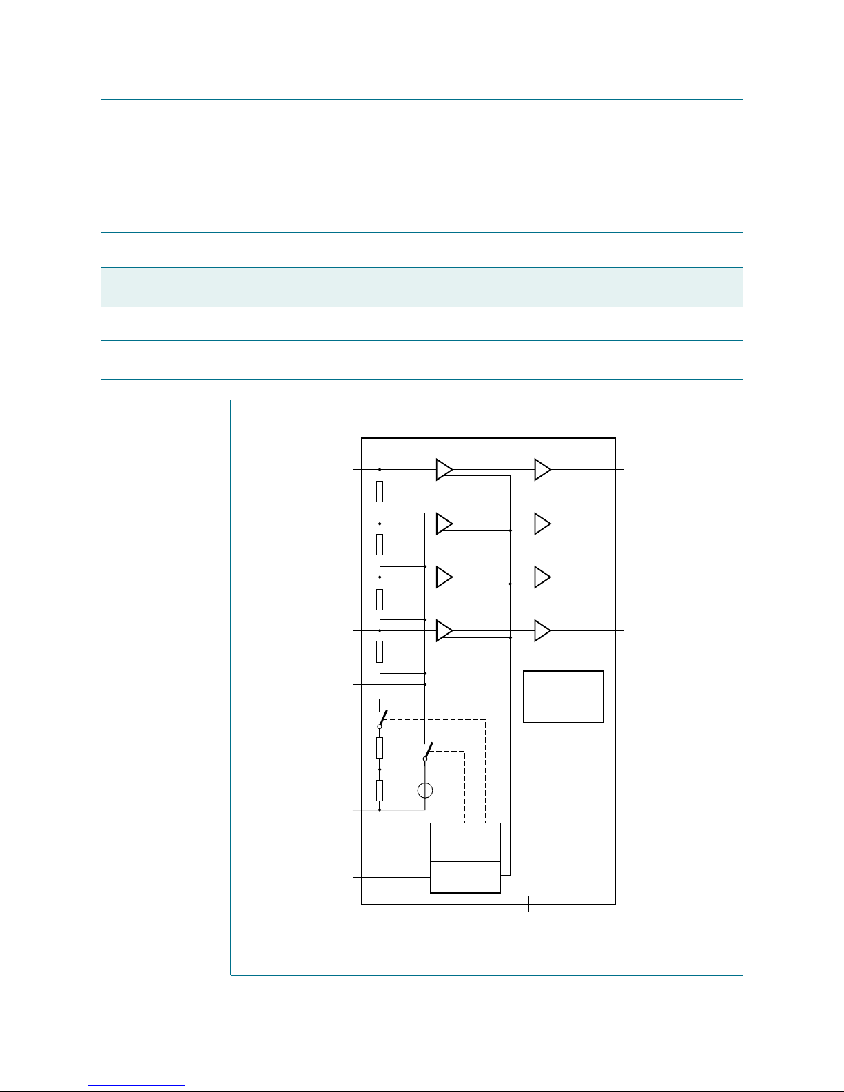
6. Block diagram
Table 2. Ordering information
Type number Package
Name Description Version
TDA8948J DBS17P DBS17P: plastic DIL-bent-SIL power package; 17 leads
(lead length 12 mm)
SOT243-1
Fig 1. Block diagram
60 kΩ
60 kΩ
V
CC1
3
V
CC2
16
8
IN1+
IN2+
OUT1+
OUT2−
6
1
4
60 kΩ
60 kΩ
9
IN3+
IN4+
OUT3−
OUT4+
12
14
17
TDA8948J
MUTE 3 + 4
ON 3 + 4
010aaa049
STANDBY ALL
MUTE ALL
ON 1 + 2
0.5V
CC
V
CC
CIV
13
MODE1
SGND
10
7
SVR
11
MODE2
5
215
GND1 GND2
SHORT-CIRCUIT
AND
TEMPERATURE
PROTECTION
V
REF
+
+
+
+
+
−
−
+
TDA8948J_1 © NXP B.V. 2008. All rights reserved.
Product data sheet Rev. 01 — 27 February 2008 4 of 26
NXP Semiconductors
TDA8948J
4-channel audio amplifier
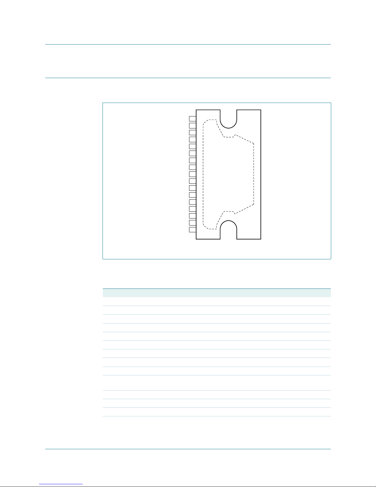
7. Pinning information
7.1 Pinning
7.2 Pin description
Fig 2. Pin configuration diagram
TDA8948J
010aaa046
1
2
3
4
5
6
7
8
9
10
11
12
13
14
15
16
17
OUT1
+
GND1
V
CC1
OUT2
−
MODE2
IN2
+
SGND
IN1
+
IN3
+
MODE1
SVR
IN4
+
CIV
OUT4
+
GND2
V
CC2
OUT3
−
Table 3. Pin description
Symbol Pin Description
OUT1+ 1 non inverted loudspeaker output of channel 1
GND1 2 ground of channels 1 and 2
V
CC1
3 supply voltage channels 1 and 2
OUT2− 4 inverted loudspeaker output of channel 2
MODE2 5 mode selection 2 input: Mute and On mode for channels 3 and 4
IN2+ 6 input channel 2
SGND 7 signal ground
IN1+ 8 input channel 1
IN3+ 9 input channel 3
MODE1 10 mode selection 1 input: Standby, Mute and On mode for all
channels
SVR 11 half supply voltage decoupling (ripple rejection)
IN4+ 12 input channel 4
CIV 13 common input voltage decoupling
OUT3− 14 inverted loudspeaker output of channel 3

TDA8948J_1 © NXP B.V. 2008. All rights reserved.
Product data sheet Rev. 01 — 27 February 2008 5 of 26
NXP Semiconductors
TDA8948J
4-channel audio amplifier
8. Functional description
8.1 Input configuration
The input cut-off frequency is:
(1)
For SE application Ri= 60 kΩ and Ci= 220 nF:
(2)
For BTL application Ri= 30 kΩ and Ci= 470 nF:
(3)
As shown in Equation 2 and Equation 3, large capacitor values for the inputs are not
necessary, so the switch-on delay during charging of the input capacitors can be
minimized. This results in a good low frequency response and good switch-on behavior.
8.2 Power amplifier
The power amplifier is a BTL and/or SE amplifier with an all-NPN output stage, capable of
delivering a peak output current of 4 A.
Using the TDA8948J as a BTL amplifier offers the following advantages:
• Low peak value of the supply current
• Ripple frequency on the supply voltage is twice the signal frequency
• No expensive DC-blocking capacitor
• Good low frequency performance
GND2 15 ground of channels 3 and 4
V
CC2
16 supply voltage channels 3 and 4
OUT4+ 17 non inverted loudspeaker output of channel 4
Table 3. Pin description
…continued
Symbol Pin Description
f
i cut off–()
1
2π RiCi×()
---------------------------- -
=
f
i cut off–()
1
2π 60 103220 109–×××()
---------------------------------------------------------------- -
12 Hz==
f
i cut off–()
1
2π 30 103470 109–×××()
---------------------------------------------------------------- -
11 Hz==

TDA8948J_1 © NXP B.V. 2008. All rights reserved.
Product data sheet Rev. 01 — 27 February 2008 6 of 26
NXP Semiconductors
TDA8948J
4-channel audio amplifier
8.2.1 Output power measurement
The output power as a function of the supply voltage is measured on the output pins at
THD = 10 %; see Figure 7.
The maximum output power is limited by the supply voltage (VCC= 26 V) and the
maximum output current (IO= 4 A repetitive peak current).
For supply voltages VCC> 22 V, a minimum load is required; see Figure 5:
• SE: R
L
=3Ω
• BTL: R
L
=6Ω
8.2.2 Headroom
Typical CD music requires at least 12 dB (factor 15.85) dynamic headroom, compared to
the average power output, for transferring the loudest parts without distortion.
The Average Listening Level (ALL) music power, without any distortion, yields:
• SE at P
o(SE)
=5W, VCC=17V, RL=4Ω and THD = 0.2 %:
(4)
• BTL at P
o(BTL)
=10W, VCC=17V, RL=8Ω and THD = 0.1 %:
(5)
The power dissipation can be derived from Figure 8 (SE and BTL) for a headroom of 0 dB
and 12 dB, respectively.
For heat sink calculation at the average listening level, a power dissipation of 9 W can be
used.
8.3 Mode selection
The TDA8948J has three functional modes which can be selected by applying the proper
DC voltage to pin MODE1.
Standby - The current consumption is very low and the outputs are floating. The device is
in standby mode when V
MODE1
< 0.8 V, or when the MODE1 pin is grounded. In standby
mode, the function of pin MODE2 has been disabled.
Mute - The amplifier is DC-biased, but not operational (no audio output). This allows the
input coupling capacitors to be charged to avoid pop-noise. The device is in mute mode
when 4.5V<V
MODE1
<(VCC- 3.5 V).
Table 4. Power rating as function of headroom
Headroom Power output Power dissipation
(all channels driven)
SE BTL
0dB P
o
=5W Po=10W P=17W
12 dB P
o(ALL)
= 315 mW P
o(ALL)
= 630 mW P = 9 W
P
oALL()SE
510
3
⋅
15.85
---------------
315 mW==
P
oALL()BTL
10 103⋅
15.85
------------------
630 mW==

TDA8948J_1 © NXP B.V. 2008. All rights reserved.
Product data sheet Rev. 01 — 27 February 2008 7 of 26
NXP Semiconductors
TDA8948J
4-channel audio amplifier
On - The amplifier is operating normally. The on mode is activated at
V
MODE1
>(VCC− 2.0 V). The output of channels 3 and 4 can be set to mute or on mode.
The output channels 3 and 4 can be switched on/off by applying a proper DC voltage to
pin MODE2, under the condition that the output channels 1 and 2 are in the on mode (see
Figure 3).
8.4 Supply voltage ripple rejection
The Supply Voltage Ripple Rejection (SVRR) is measured with an electrolytic capacitor of
150 µF on pin SVR using a bandwidth of 20 Hz to 22 kHz. Figure 10 illustrates the SVRR
as function of the frequency. A larger capacitor value on pin SVR improves the ripple
rejection behavior at the lower frequencies.
Table 5. Mode selection
Voltage on pin Channel 1 and 2 Channel 3 and 4
(sub woofer)
MODE1 MODE2
0 V to 0.8 V 0 V to V
CC
Standby mode Standby mode
4.5 V to (V
CC
− 3.5 V) 0 V to V
CC
Mute mode Mute mode
(V
CC
− 2.0 V) to V
CC
0 V to (VCC− 3.5 V) On mode Mute mode
(V
CC
− 2 V) to V
CC
On mode On mode
Fig 3. Mode selection
mdb016
channels 3 + 4: mute
channels 1 + 2: on
channels 3 + 4: on or mute
channels 3 + 4: on
V
CC
−3.5 V
CC
V
MODE2
VCC−2.0
all standby
all mute
0.8 4.5 V
CC
−3.5
V
CC
V
MODE1
VCC−2.0

TDA8948J_1 © NXP B.V. 2008. All rights reserved.
Product data sheet Rev. 01 — 27 February 2008 8 of 26
NXP Semiconductors
TDA8948J
4-channel audio amplifier
8.5 Built-in protection circuits
The TDA8948Jcontains two types of detection sensors: one measures local temperatures
of the power stages and one measures the global chip temperature. At a local
temperature of approximately 185 °C or a global temperature of approximately 150 °C,
this detection circuit switches off the power stages for 2 ms. High-impedance of the
outputs is the result. After this time period the power stages switch on automatically and
the detection will take place again; still a too high temperature switches off the power
stages immediately. This protects the TDA8948J against shorts to ground, to the supply
voltage and across the load, and against too high chip temperatures.
The protection will only be activated when necessary, so even during a short-circuit
condition, a certain amount of (pulsed) current will still be flowing through the short,just as
much as the power stage can handle without exceeding the critical temperature level.
9. Limiting values
[1] The amplifier can deliver output power with non-clipping output signals into nominal loads as long as the
ratings of the IC are not exceeded.
10. Thermal characteristics
Table 6. Limiting values
In accordance with the Absolute Maximum Rating System (IEC 60134).
Symbol Parameter Conditions Min Max Unit
V
CC
supply voltage operating −0.3 +26 V
no (clipping) signal
[1]
−0.3 +28 V
V
I
input voltage - −0.3 VCC+ 0.3 V
I
ORM
repetitive peak output
current
--4A
T
stg
storage temperature non-operating −55 +150 °C
T
amb
ambient temperature - −40 +85 °C
P
tot
total power dissipation - - 69 W
V
CC(sc)
supply voltage (short circuit) - - 24 V
Table 7. Thermal characteristics
Symbol Parameter Conditions Typ Unit
R
th(j-a)
thermal resistance from junction
to ambient
in free air 40 K/W
R
th(j-c)
thermal resistance from junction
to case
all channels driven 2 K/W
 Loading...