

Page 1

TDA8932B
Class-D audio amplifier
Rev. 03 — 21 June 2007 Product data sheet
1. General description
The TDA8932B is a high efficiency class-D amplifier with low power dissipation.
The continuous time output power is 2 × 15 W in stereo half-bridge application (RL=4Ω)
or 1 × 30 W in mono full-bridge application (RL=8Ω). Due to the low power dissipation
the device can be used without any external heat sink when playing music. Due to the
implementation of thermal foldback, even for high supply voltages and/or lower load
impedances, the device remains operating with considerable music output power without
the need for an external heat sink.
The device has two full-differential inputs driving two independent outputs. It can be used
as mono full-bridge configuration (BTL) or as stereo half-bridge configuration (SE).
2. Features
n Operating voltage from 10 V to 36 V asymmetrical or ±5 V to ±18 V symmetrical
n Mono-bridged tied load (full-bridge) or stereo single-ended (half-bridge) application
n Application without heatsink using thermally enhanced small outline package
n High efficiency and low-power dissipation
n Thermally protected and thermal foldback
n Current limiting to avoid audio holes
n Full short-circuit proof across load and to supply lines (using advanced current
n Switchable internal or external oscillator (master-slave setting)
n No pop noise
n Full-differential inputs
3. Applications
n Flat panel television sets
n Flat panel monitor sets
n Multimedia systems
n Wireless speakers
n Mini and micro systems
n Home sound sets
protection)
Page 2

NXP Semiconductors
4. Quick reference data
Table 1. Quick reference data
VP= 22 V; f
Symbol Parameter Conditions Min Typ Max Unit
Supplies
V
P
I
P
I
q(tot)
Stereo SE channel; R
P
o(RMS)
Mono BTL; R
P
o(RMS)
osc
supply voltage asymmetrical supply 10 22 36 V
supply current Sleep mode - 0.6 1.0 mA
total quiescent
current
RMS output power continuous time output power
RMS output power continuous time output power;
= 320 kHz; T
< 0.1 Ω
s
[1]
< 0.1 Ω
s
TDA8932B
Class-D audio amplifier
=25°C; unless otherwise specified.
amb
Operating mode; no load, no
snubbers and no filter
connected
[1]
per channel;
THD+N = 10 %; f
=4Ω; VP= 22 V 13.8 15.3 - W
R
L
=8Ω; VP= 30 V 14.0 15.5 - W
R
L
= 1 kHz
i
short time output power per
channel; THD+N = 10 %;
f
= 1 kHz
i
RL=4Ω; VP= 29 V 23.8 26.5 - W
THD+N = 10 %; f
=4Ω; VP= 12 V 15.5 17.2 - W
R
L
=8Ω; VP= 22 V 28.9 32.1 - W
R
L
= 1 kHz
i
short time output power;
THD+N = 10 %; f
= 1 kHz
i
RL=8Ω; VP= 29 V 49.5 55.0 - W
- 4050mA
[2]
[2]
[1] Output power is measured indirectly; based on R
[2] Two layer application board (55 mm × 45 mm), 35 µm copper, FR4 base material in free air with natural
convection.
measurement.
DSon
5. Ordering information
Table 2. Ordering information
Type number Package
Name Description Version
TDA8932BT SO32 plastic small outline package; 32 leads;
body width 7.5 mm
TDA8932BTW HTSSOP32 plastic thermal enhanced thin shrink small outline
package; 32 leads; body width 6.1 mm; lead pitch
0.65 mm; exposed die pad
TDA8932B_3 © NXP B.V. 21 June 2007. All rights reserved.
Product data sheet Rev. 03— 21 June 2007 2 of 48
SOT287-1
SOT549-1
Page 3
NXP Semiconductors
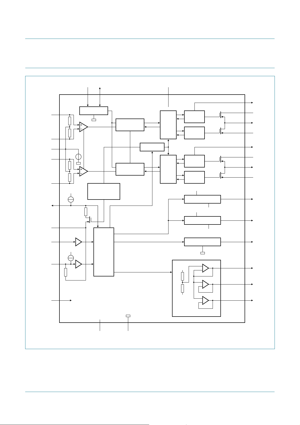
6. Block diagram
TDA8932B
Class-D audio amplifier
IN1P
IN1N
INREF
IN2P
IN2N
DIAG
CGND
OSCREF OSCIO V
10 31 8
2
3
12
15
14
4
7
OSCILLATOR
V
SSD
PROTECTIONS:
OVP, OCP, OTP,
UVP, TF, WP
PWM
MODULATOR
MANAGER
PWM
MODULATOR
DDA
CTRL
CTRL
DRIVER
HIGH
DRIVER
LOW
DRIVER
HIGH
DRIVER
LOW
V
DDA
STABILIZER 11 V
V
SSP1
V
DDA
STABILIZER 11 V
V
SSP2
28
BOOT1
29
V
DDP1
27
OUT1
26
V
SSP1
21
BOOT2
20
V
DDP2
22
OUT2
23
V
SSP2
25
STAB1
24
STAB2
POWERUP
ENGAGE
TEST
6
5
13
Fig 1. Block diagram
MODE
V
SSA
9
TDA8932B
V
SSD(HW)
1, 16, 17, 32
REGULATOR 5 V
V
SSD
V
DDA
V
SSA
HALF SUPPLY VOLTAGE
18
11
30
19
001aaf597
DREF
HVPREF
HVP1
HVP2
TDA8932B_3 © NXP B.V. 21 June 2007. All rights reserved.
Product data sheet Rev. 03— 21 June 2007 3 of 48
Page 4
NXP Semiconductors
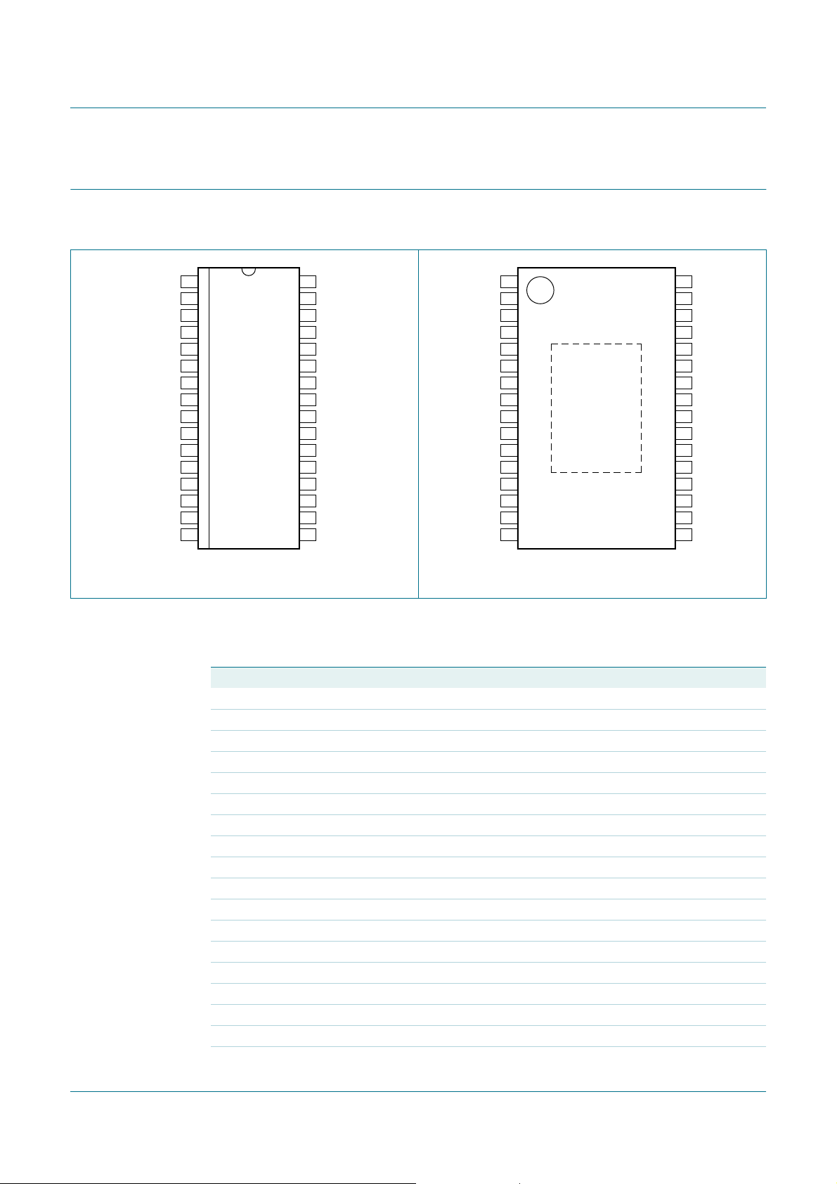
7. Pinning information
7.1 Pinning
TDA8932B
Class-D audio amplifier
V
SSD(HW)
ENGAGE BOOT1
POWERUP OUT1
OSCREF
HVPREF OUT2
V
SSD(HW)
1
2
IN1P OSCIO
3
IN1N HVP1
4
DIAG V
5
6
7
CGND V
8
V
DDA
V
SSA
INREF BOOT2
TEST V
IN2N HVP2
IN2P DREF
9
10
11
12
13
14
15
16
TDA8932BT
001aaf598
32
31
30
29
28
27
26
25
24
23
22
21
20
19
18
17
V
SSD(HW)
DDP1
SSP1
STAB1
STAB2
V
SSP2
DDP2
V
SSD(HW)
V
SSD(HW)
ENGAGE BOOT1
POWERUP OUT1
OSCREF V
HVPREF OUT2
V
SSD(HW)
1
2
IN1P OSCIO
3
IN1N HVP1
4
DIAG V
5
6
7
CGND V
8
V
DDA
9
V
SSA
10
11
12
INREF BOOT2
13
TEST V
14
IN2N HVP2
15
IN2P DREF
16
TDA8932BTW
Fig 2. Pin configuration SO32 Fig 3. Pin configuration HTSSOP32
7.2 Pin description
Table 3. Pin description
Symbol Pin Description
V
SSD(HW)
IN1P 2 positive audio input for channel 1
IN1N 3 negative audio input for channel 1
DIAG 4 diagnostic output; open-drain
ENGAGE 5 engage input to switch between Mute mode and Operating mode
POWERUP 6 power-up input to switch between Sleep mode and Mute mode
CGND 7 control ground; reference for POWERUP, ENGAGE and DIAG
V
DDA
V
SSA
OSCREF 10 input internal oscillator setting (only master setting)
HVPREF 11 decoupling of internal half supply voltage reference
INREF 12 decoupling for input reference voltage
TEST 13 test signal input; for testing purpose only
IN2N 14 negative audio input for channel 2
IN2P 15 positive audio input for channel 2
V
SSD(HW)
V
SSD(HW)
DREF 18 decoupling of internal (reference) 5 V regulator for logic supply
1 negative digital supply voltage and handle wafer connection
8 positive analog supply voltage
9 negative analog supply voltage
16 negative digital supply voltage and handle wafer connection
17 negative digital supply voltage and handle wafer connection
001aaf599
32
31
30
29
28
27
26
25
24
23
22
21
20
19
18
17
V
SSD(HW)
DDP1
SSP1
STAB1
STAB2
SSP2
DDP2
V
SSD(HW)
TDA8932B_3 © NXP B.V. 21 June 2007. All rights reserved.
Product data sheet Rev. 03— 21 June 2007 4 of 48
Page 5

NXP Semiconductors
Table 3. Pin description (Continued)
Symbol Pin Description
HVP2 19 half supply output voltage 2 for charging single-ended capacitor for
V
DDP2
BOOT2 21 bootstrap high-side driver channel 2
OUT2 22 PWM output channel 2
V
SSP2
STAB2 24 decoupling of internal 11 V regulator for channel 2 drivers
STAB1 25 decoupling of internal 11 V regulator for channel 1 drivers
V
SSP1
OUT1 27 PWM output channel 1
BOOT1 28 bootstrap high-side driver channel 1
V
DDP1
HVP1 30 half supply output voltage 1 for charging single-ended capacitor for
OSCIO 31 oscillator input in slave configuration or oscillator output in master
V
SSD(HW)
Exposed die
pad
TDA8932B
Class-D audio amplifier
channel 2
20 positive power supply voltage for channel 2
23 negative power supply voltage for channel 2
26 negative power supply voltage for channel 1
29 positive power supply voltage for channel 1
channel 1
configuration
32 negative digital supply voltage and handle wafer connection
- HTSSOP32 package only
[1]
[1] The exposed die pad has to be connected to V
8. Functional description
8.1 General
The TDA8932B is a mono full-bridge or stereo half-bridge audio power amplifier using
class-D technology. The audio input signal is converted into a Pulse Width Modulated
(PWM) signal via an analog input stage and PWM modulator. To enable the output power
Diffusion Metal Oxide Semiconductor (DMOS) transistors to be driven, this digital PWM
signal is applied to a control and handshake block and driver circuits forboth the high side
and low side. A 2nd-order low-pass filter converts the PWM signal to an analog audio
signal across the loudspeakers.
The TDA8932B contains two independent half-bridges with full differential input stages.
The loudspeakers can be connected in the following configurations:
• Mono full-bridge: Bridge Tied Load (BTL)
• Stereo half-bridge: Single-Ended (SE)
The TDA8932B contains common circuits to both channels such as the oscillator, all
reference sources, the mode functionality and a digital timing manager. The following
protections are built-in: thermal foldback, temperature, current and voltage protections.
SSD(HW)
.
TDA8932B_3 © NXP B.V. 21 June 2007. All rights reserved.
Product data sheet Rev. 03— 21 June 2007 5 of 48
Page 6
NXP Semiconductors
8.2 Mode selection and interfacing
The TDA8932B can be switched in three operating modes using pins POWERUP and
ENGAGE:
• Sleep mode: with low supply current.
• Mutemode: the amplifiers are switching idle (50 % duty cycle), but the audio signal at
• Operating mode: the amplifiers are fully operational with output signal.
• Fault mode.
Both pins POWERUP and ENGAGE refer to pin CGND.
Table 4 shows the different modes as a function of the voltages on the POWERUP and
ENGAGE pins.
Table 4. Mode selection
Mode Pin
Sleep < 0.8 V < 0.8 V don’t care
Mute 2 V to 6.0 V
Operating 2 V to 6.0 V
Fault 2 V to 6.0 V
TDA8932B
Class-D audio amplifier
the output is suppressed bydisabling the Vl-converter input stages. The capacitors on
pins HVP1 and HVP2 have been charged to half the supply voltage (asymmetrical
supply only).
POWERUP ENGAGE DIAG
[1]
[1]
[1]
[1]
< 0.8 V
2.4 V to 6.0 V
don’t care < 0.8 V
[1]
> 2 V
>2V
[1] In case of symmetrical supply conditions the voltage applied to pins POWERUP and ENGAGE must never
exceed the supply voltage (V
DDA
, V
DDP1
or V
DDP2
).
If the transition between Mute mode and Operatingmode is controlled via a time constant,
the start-up will be pop free since the DC output offset voltage is applied gradually to the
output between Mute mode and Operating mode. The bias current setting of the
VI-converters is related to the voltage on pin ENGAGE:
• Mute mode: the bias current setting of the VI-converters is zero (VI-converters
disabled)
• Operating mode: the bias current is at maximum
The time constant required to apply the DC output offset voltage gradually between Mute
mode and Operating mode can be generated by applying a decoupling capacitor on pin
ENGAGE. The value of the capacitor on pin ENGAGE should be 470 nF.
TDA8932B_3 © NXP B.V. 21 June 2007. All rights reserved.
Product data sheet Rev. 03— 21 June 2007 6 of 48
Page 7
NXP Semiconductors
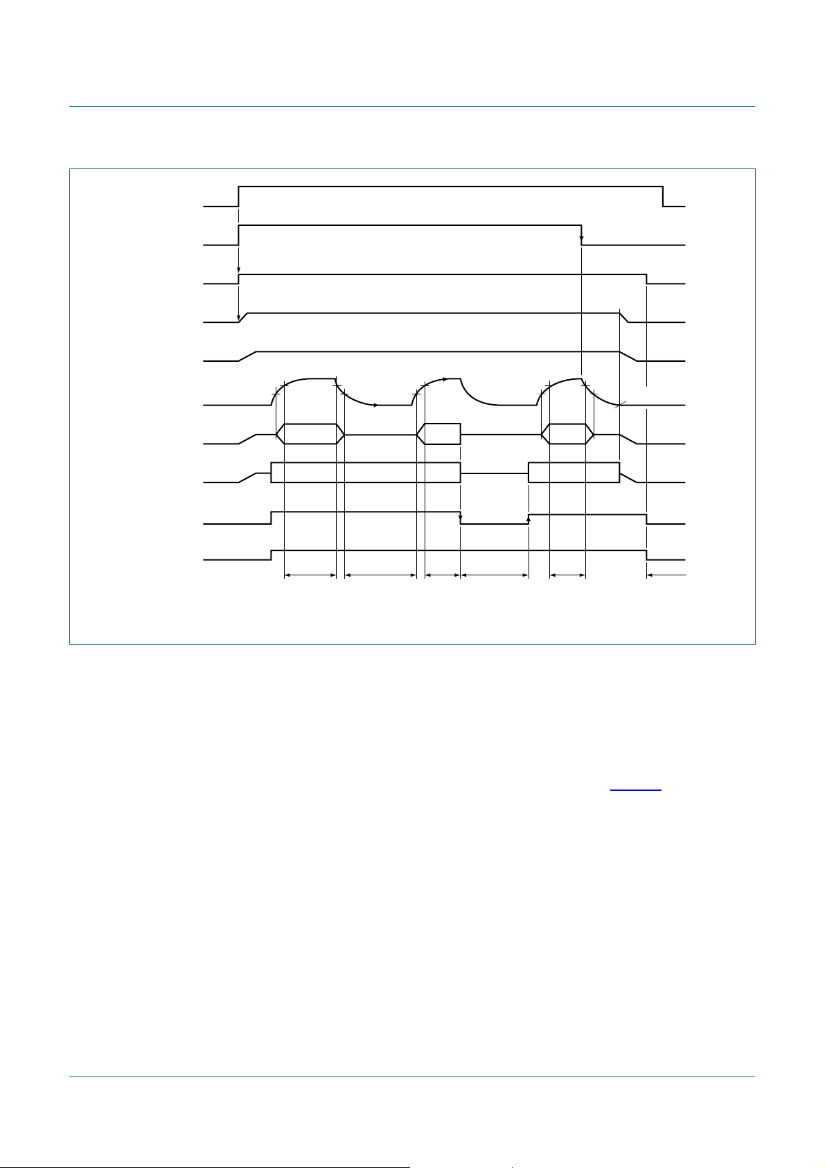
V
P
POWERUP
DREF
HVPREF
HVP1, HVP2
2.0 V (typical)
ENGAGE
1.2 V (typical)
TDA8932B
Class-D audio amplifier
≤ 0.8 V
audio
OUT1, OUT2
PWM
DIAG
OSCIO
Fig 4. Start-up sequence
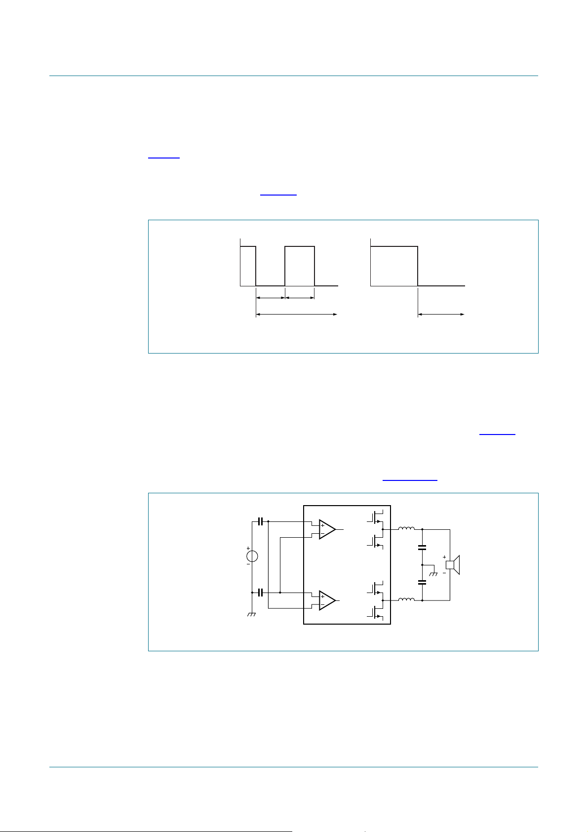
8.3 Pulse width modulation frequency
The output signal of the amplifier is a PWM signal with a carrier frequency of
approximately 320 kHz. Using a 2nd-order low-pass filter in the application results in an
analog audio signal across the loudspeaker. The PWM switching frequency can be set by
an external resistor Rosc connected between pins OSCREF and V
frequency can be set between 300 kHz and 500 kHz. Using an external resistor of 39 kΩ,
the carrier frequency is set to an optimized value of 320 kHz (see Figure 5).
If two or more TDA8932B devices are used in the same audio application, it is
recommended to synchronize the switching frequency of all devices. This can be realized
by connecting all pins OSCIO together and configure one of the TDA8932B in the
application as clock master, while the other TDA8932B devices are configured in slave
mode.
AUDIO AUDIO AUDIO
PWMPWM
operating operating
001aaf885
SSD(HW)
sleepmute operating fault
. The carrier
Pin OSCIO is a 3-state input or output buffer.Pin OSCIO is configured in master mode as
oscillator output and in slave modeas oscillator input. Master mode is enabled byapplying
a resistor while slave mode is entered by connecting pin OSCREF directly to pin V
SSD(HW)
(without any resistor).
The value of the resistor also sets the frequency of the carrier which can be estimated by
the following formula:
TDA8932B_3 © NXP B.V. 21 June 2007. All rights reserved.
Product data sheet Rev. 03— 21 June 2007 7 of 48
Page 8
NXP Semiconductors
TDA8932B
Class-D audio amplifier
osc
12.45 109×
=
--------------------------- -
Rosc
f
Where:
f
= oscillator frequency (Hz)
osc
Rosc = oscillator resistor (on pin OSCREF) (Ω)
550
f
osc
(kHz)
450
350
250
25 454030 35
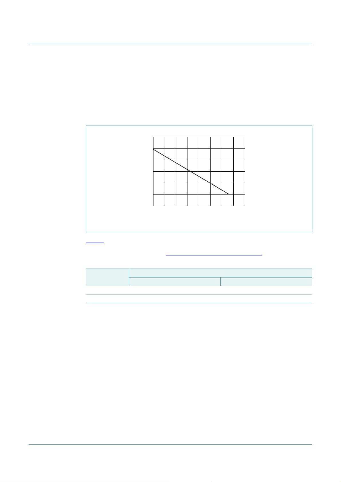
Fig 5. Oscillation frequency as a function of resistor Rosc
(1)
001aad758
Rosc (kΩ)
Table 5 summarizes how to configure the TDA8932B in master or slave configuration.
For device synchronization see Section 14.6 “Device synchronization”.
Table 5. Master or slave configuration
Configuration Pin
OSCREF OSCIO
Master Rosc > 25 kΩ to V
Slave Rosc = 0 Ω; shorted to V
SSD(HW)
SSD(HW)
output
input
8.4 Protection
The following protection is included in the TDA8932B:
• Thermal Foldback (TF)
• OverTemperature Protection (OTP)
• OverCurrent Protection (OCP)
• Window Protection (WP)
• Supply voltage protection:
– UnderVoltage Protection (UVP)
– OverVoltage Protection (OVP)
– UnBalance Protection (UBP)
• ElectroStatic Discharge (ESD)
The reaction of the device to the different fault conditions differs per protection.
TDA8932B_3 © NXP B.V. 21 June 2007. All rights reserved.
Product data sheet Rev. 03— 21 June 2007 8 of 48
Page 9

NXP Semiconductors
8.4.1 Thermal Foldback (TF)
If the junction temperature of the TDA8932B exceeds the threshold level (Tj> 140 °C) the
gain of the amplifier is decreased graduallyto a level where the combination of dissipation
(P) and the thermal resistance from junction to ambient [R
temperature around the threshold level.
This means that the device will not completely switch off, but remains operational at lower
output power levels. Especially with music output signals this feature enables high peak
output power while still operating without any external heat sink other than the
printed-circuit board area.
If the junction temperature still increases due to external causes, the OTP shuts down the
amplifier completely.
8.4.2 OverTemperature Protection (OTP)
If the junction temperature Tj> 155 °C, then the power stage will shut down immediately.
8.4.3 OverCurrent Protection (OCP)
When the loudspeaker terminals are short-circuited or if one of the demodulated outputs
of the amplifier is short-circuited to one of the supply lines, this will be detected by the
OCP.
TDA8932B
Class-D audio amplifier
] results in a junction
th(j-a)
If the output current exceeds the maximum output current (I
be limitedby the amplifier to 4 A while the amplifier outputs remain switching (the amplifier
is NOT shutdown completely). This is called current limiting.
The amplifier can distinguish between an impedance drop of the loudspeaker and a
low-ohmic short-circuit across the load or to one of the supply lines. This impedance
threshold depends on the supply voltage used:
• Incase of a short-circuit across the load, the audio amplifier is switchedoff completely
and after approximately 100 ms it will try to restart again. If the short-circuit condition
is still present after this time, this cycle will be repeated. The average dissipation will
be low because of this low duty cycle.
• In case of a short to one of the supply lines, this will trigger the OCP and the amplifier
will be shut down. During restart the window protection will be activated. As a result
the amplifier will not start until 100 ms after the short to the supply lines is removed.
• In case of impedance drop (e.g. due to dynamic behavior of the loudspeaker) the
same protection will be activated. The maximum output current is again limited to 4 A,
but the amplifier will NOT switch off completely (thus preventing audio holes from
occurring). The result will be a clipping output signal without any artifacts.
8.4.4 Window Protection (WP)
The WP checks the PWM output voltage before switchingfrom Sleep mode to Mute mode
(outputs switching) and is activated:
> 4 A), this current will
O(ocp)
• During the start-up sequence, when pin POWERUP is switched from Sleep mode to
Mute mode. In the event of a short-circuit at one of the output terminals to V
V
, V
SSP1
for open-circuit outputs. Because the check is done before enablingthe power stages,
no large currents will flow in the event of a short-circuit.
TDA8932B_3 © NXP B.V. 21 June 2007. All rights reserved.
Product data sheet Rev. 03— 21 June 2007 9 of 48
DDP2
or V
the start-up procedure is interrupted and the TDA8932B waits
SSP2
DDP1
,
Page 10

NXP Semiconductors
• When the amplifier is completely shut down due to activation of the OCP because a
8.4.5 Supply voltage protection
If the supply voltage drops below 10 V, the UnderVoltage Protection (UVP) circuit is
activated and the system will shut down directly. This switch-off will be silent and without
pop noise. When the supply voltage rises above the threshold level, the system is
restarted again after 100 ms.
If the supply voltage exceeds 36 V the OverVoltage Protection (OVP) circuit is activated
and the power stages will shut down. It is re-enabled as soon as the supply voltage drops
below the threshold level. The system is restarted again after 100 ms.
It should be noted that supply voltages > 40 V may damage the TDA8932B. Two
conditions should be distinguished:
1. If the supply voltage is pumped to higher values by the TDA8932B application itself
2. If a supply voltage > 40 V is caused by other or external causes, then the TDA8932B
TDA8932B
Class-D audio amplifier
short-circuit to one of the supply lines is made, then during restart (after 100 ms) the
window protection will be activated. As a result the amplifier will not start until the
short-circuit to the supply lines is removed.
(see also Section 14.3), the OVP is triggered and the TDA8932B is shut down. The
supply voltage will decrease and the TDA8932B is protected against any overstress.
will shut down, but the device can still be damaged since the supply voltage will
remain > 40 V in this case. The OVP protection is not a supply voltage clamp.
An additional UnBalance Protection (UBP) circuit compares the positive analog supply
voltage (V
) and the negative analog supply voltage (V
DDA
) and is triggered if the
SSA
voltage difference between them exceeds a certain level. This level depends on the sum
of both supply voltages. The unbalance threshold levels can be defined as follows:
• LOW-level threshold: V
• HIGH-level threshold: V
P(th)(ubp)l
P(th)(ubp)h
<8⁄5× V
>8⁄3× V
HVPREF
HVPREF
In a symmetrical supply the UBP is released when the unbalance of the supply voltage is
within 6 % of its starting value.
Table 6 shows an overview of all protection and the effect on the output signal.
Table 6. Protection overview
Protection Restart
When fault is removed Every 100 ms
OTP no yes
OCP yes no
WP yes no
UVP no yes
OVP no yes
UBP no yes
TDA8932B_3 © NXP B.V. 21 June 2007. All rights reserved.
Product data sheet Rev. 03— 21 June 2007 10 of 48
Page 11
NXP Semiconductors
8.5 Diagnostic input and output
Whenevera protection is triggered, except for TF, pin DIAG is activated to LOWlevel (see
Table 6). An internal reference supply will pull-up the open-drain DIAG output to
approximately 2.4 V. This internal reference supply can deliver approximately 50 µA.
Pin DIAG refers to pin CGND. The diagnostic output signal during different short
conditions is illustrated in Figure 6. Using pin DIAG as input, a voltage < 0.8 V will put the
device into Fault mode.
TDA8932B
Class-D audio amplifier
V
2.4 V
0 V
o
amplifier
restart no restart
≈ 50 ms
≈ 50 ms
shorted load
2.4 V
0 V
V
o
short to
supply line
001aad759
Fig 6. Diagnostic output for different short-circuit conditions
8.6 Differential inputs
For a high common-mode rejection ratio and a maximum of flexibility in the application,
the audio inputs are fully differential. By connecting the inputs anti-parallel, the phase of
one of the two channels can be inverted, so that the amplifier can operate as a mono BTL
amplifier. The input configuration for a mono BTL application is illustrated in Figure 7.
In SE configuration it is also recommended to connect the two differential inputs in
anti-phase. This has advantages forthe current handling of the power supply at low signal
frequencies and minimizes supply pumping (see also Section 14.8).
IN1P
IN1N
OUT1
audio
input
IN2P
IN2N
OUT2
001aad760
Fig 7. Input configuration for mono BTL application
8.7 Output voltage buffers
When pin POWERUP is set HIGH, the half supply output voltage buffers are switched on
in asymmetrical supply configuration. The start-up will be pop free since the device starts
switching when the capacitor on pin HVPREF and the SE capacitors are completely
charged.
Output voltage buffers:
TDA8932B_3 © NXP B.V. 21 June 2007. All rights reserved.
Product data sheet Rev. 03— 21 June 2007 11 of 48
Page 12
NXP Semiconductors
• PinsHVP1 and HVP2: The time requiredfor charging the SE capacitor depends on its
value. The half supply voltage output is disabled when the TDA8932B is used in a
symmetrical supply application.
• Pin HVPREF: This output voltage reference buffer charges the capacitor on pin
HVPREF.
• PinINREF: This output voltage reference buffercharges the input referencecapacitor
on pin INREF. Pin INREF applies the bias voltage for the inputs.
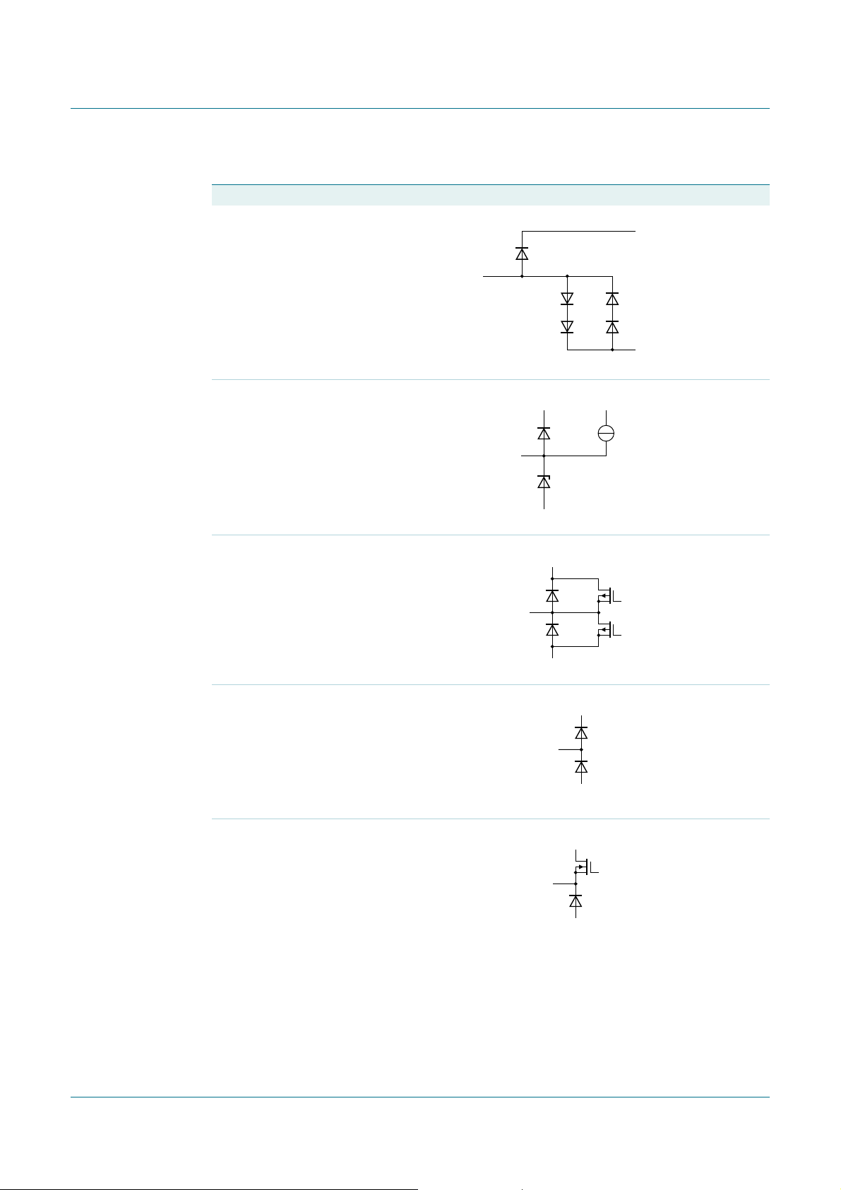
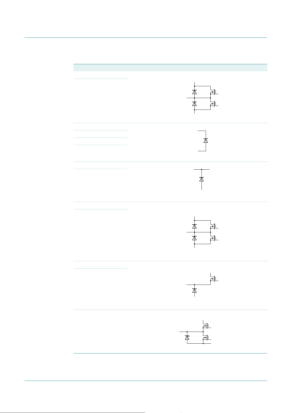
9. Internal circuitry
Table 7. Internal circuitry
Pin Symbol Equivalent circuit
1V
16 V
17 V
32 V
SSD(HW)
SSD(HW)
SSD(HW)
SSD(HW)
1, 16,
17, 32
TDA8932B
Class-D audio amplifier
V
DDA
V
SSA
001aad784
2 IN1P
3 IN1N
12 INREF
14 IN2N
15 IN2P
4 DIAG
2, 15
12
3, 14
V
DDA
2 kΩ
± 20 %
48 kΩ
± 20 %
48 kΩ
± 20 %
2 kΩ
± 20 %
V
SSA
V
DDA
4
2.5 V
50 µA
500 Ω
± 20 %
100 kΩ
± 20 %
V/I
HVPREF
V/I
001aad785
V
SSA
TDA8932B_3 © NXP B.V. 21 June 2007. All rights reserved.
CGND
001aaf607
Product data sheet Rev. 03— 21 June 2007 12 of 48
Page 13
NXP Semiconductors
Table 7. Internal circuitry (Continued)
Pin Symbol Equivalent circuit
5 ENGAGE
TDA8932B
Class-D audio amplifier
2 kΩ
± 20 %
2.8 V
I
ref
= 50 µA
V
DDA
5
100 kΩ
± 20 %
6 POWERUP
7 CGND
SSA
CGND
V
DDA
V
SSA
CGND
V
DDA
7
V
SSA
001aad789
001aaf608
001aad788
V
6
8V
TDA8932B_3 © NXP B.V. 21 June 2007. All rights reserved.
DDA
8
V
SSA
V
SSD
001aad790
Product data sheet Rev. 03— 21 June 2007 13 of 48
Page 14
NXP Semiconductors
Table 7. Internal circuitry (Continued)
Pin Symbol Equivalent circuit
9V
SSA
TDA8932B
Class-D audio amplifier
V
DDA
9
V
SSD
001aad791
10 OSCREF
11 HVPREF
13 TEST
V
DDA
I
ref
10
V
SSA
V
11
V
13
DDA
SSA
V
V
001aad795
001aad792
001aaf604
DDA
SSA
18 DREF
V
DD
18
V
SSD
001aag025
TDA8932B_3 © NXP B.V. 21 June 2007. All rights reserved.
Product data sheet Rev. 03— 21 June 2007 14 of 48
Page 15
NXP Semiconductors
Table 7. Internal circuitry (Continued)
Pin Symbol Equivalent circuit
19 HVP2
30 HVP1
19, 30
V
V
DDA
SSA
TDA8932B
Class-D audio amplifier
001aag026
20 V
23 V
26 V
29 V
DDP2
SSP2
SSP1
DDP1
21 BOOT2
28 BOOT1
22 OUT2
27 OUT1
24 STAB2
25 STAB1
22, 27
20, 29
23, 26
21, 28
V
V
V
V
001aad798
OUT1, OUT2
001aad799
DDP1,
DDP2
SSP1,
SSP2
001aag027
V
DDA
24, 25
V
SSP1,
V
SSP2
001aag028
31 OSCIO
DREF
31
V
SSD
001aag029
TDA8932B_3 © NXP B.V. 21 June 2007. All rights reserved.
Product data sheet Rev. 03— 21 June 2007 15 of 48
Page 16

NXP Semiconductors
10. Limiting values
Table 8. Limiting values
In accordance with the Absolute Maximum Rating System (IEC 60134).
Symbol Parameter Conditions Min Max Unit
V
P
V
x
I
ORM
T
j
T
stg
T
amb
P power dissipation - 5 W
V
esd
TDA8932B
Class-D audio amplifier
supply voltage asymmetrical supply
voltage on pin x
IN1P, IN1N, IN2P, IN2N
OSCREF, OSCIO, TEST
POWERUP, ENGAGE,
DIAG
all other pins
repetitive peak output
current
maximum output
current limiting
junction temperature - 150 °C
storage temperature −55 +150 °C
ambient temperature −40 +85 °C
electrostatic discharge
voltage
HBM
MM
[1]
−0.3 +40 V
[2]
−5+5V
[3]
V
SSD(HW)
[4]
V
CGND
[5]
VSS− 0.3 VDD + 0.3 V
[6]
4-A
[7]
−2000 +2000 V
[8]
−200 +200 V
− 0.3 5 V
− 0.3 6 V
[1] VP = V
[2] Measured with respect to pin INREF; Vx < VDD + 0.3 V.
[3] Measured with respect to pin V
[4] Measured with respect to pin CGND; Vx < VDD + 0.3 V.
[5] VSS = V
[6] Current limiting concept.
[7] Human Body Model (HBM); Rs= 1500 Ω; C = 100 pF
For pins 2, 3, 11, 14 and 15 V
[8] Machine Model (MM); Rs=0Ω; C = 200 pF; L = 0.75 µH.
DDP1
SSP1
− V
= V
SSP1
SSP2
= V
DDP2
; VDD = V
− V
SSD(HW)
DDP1
esd
SSP2
.
; Vx < VDD + 0.3 V.
= V
= ±1800 V.
DDP2
.
11. Thermal characteristics
Table 9. Thermal characteristics
Symbol Parameter Conditions Min Typ Max Unit
SO32 package
R
Ψ
Ψ
th(j-a)
j-lead
j-top
thermal resistance from junction
to ambient
thermal characterization
parameter from junction to lead
thermal characterization
parameter from junction to top
free air natural convection
JEDEC test board
2 layer application board
[1]
- 41 44 K/W
[2]
- 44 - K/W
- - 30 K/W
[3]
- - 8 K/W
TDA8932B_3 © NXP B.V. 21 June 2007. All rights reserved.
Product data sheet Rev. 03— 21 June 2007 16 of 48
Page 17

NXP Semiconductors
TDA8932B
Class-D audio amplifier
Table 9. Thermal characteristics (Continued)
Symbol Parameter Conditions Min Typ Max Unit
HTSSOP32 package
R
th(j-a)
thermal resistance from junction
to ambient
Ψ
j-lead
thermal characterization
parameter from junction to lead
Ψ
j-top
thermal characterization
parameter from junction to top
R
th(j-c)
thermal resistance from junction
to case
[1] Measured on a JEDEC high K-factor test board (standard EIA/JESD 51-7) in free air with natural convection.
[2] Two layer application board (55 mm × 45 mm), 35 µm copper, FR4 base material in free air with natural convection.
[3] Strongly depends on where the measurement is taken on the package.
[4] Two layer application board (55 mm × 40 mm), 35 µm copper, FR4 base material in free air with natural convection.
free air natural convection
[1]
JEDEC test board
2 layer application board
- 47 50 K/W
[4]
- 48 - K/W
- - 30 K/W
[3]
- - 2 K/W
free air natural convection - 4.0 - K/W
12. Static characteristics
Table 10. Static characteristics
VP= 22 V; f
Symbol Parameter Conditions Min Typ Max Unit
Supply
V
P
I
P
I
q(tot)
Series resistance output power switches
R
DSon
Power-up input: pin POWERUP
V
I
I
I
V
IL
V
IH
Engage input: pin ENGAGE
V
O
V
I
I
O
V
IL
V
IH
= 320 kHz; T
osc
=25°C; unless otherwise specified.
amb
supply voltage asymmetrical supply 10 22 36 V
symmetrical supply ±5 ±11 ±18 V
supply current Sleep mode; no load - 0.6 1.0 mA
total quiescent current Operating mode; no load, no
- 4050mA
snubbers and no filter connected
drain-source on-state
resistance
[1]
Tj=25°C - 150 - mΩ
= 125 °C - 234 - mΩ
T
j
input voltage 0 - 6.0 V
input current VI=3V - 1 20 µA
LOW-level input voltage 0 - 0.8 V
HIGH-level input voltage 2 - 6.0 V
[1]
output voltage open pin 2.4 2.8 3.1 V
input voltage 0 - 6.0 V
output current VI= 0 V - 50 60 µA
LOW-level input voltage 0 - 0.8 V
HIGH-level input voltage 2.4 - 6.0 V
TDA8932B_3 © NXP B.V. 21 June 2007. All rights reserved.
Product data sheet Rev. 03— 21 June 2007 17 of 48
Page 18

NXP Semiconductors
TDA8932B
Class-D audio amplifier
Table 10. Static characteristics (Continued)
VP= 22 V; f
Symbol Parameter Conditions Min Typ Max Unit
Diagnostic output: pin DIAG
V
O
Bias voltage for inputs: pin INREF
V
O(bias)
Half supply voltage
Pins HVP1 and HVP2
V
O
I
O
Pin HVPREF
V
O
Reference voltage for internal logic: pin DREF
V
O
Amplifier outputs: pins OUT1 and OUT2
|V
O(offset)
Stabilizer output: pins STAB1 and STAB2
V
O
Voltage protection
V
P(uvp)
V
P(ovp)
V
P(th)(ubp)l
V
P(th)(ubp)h
Current protection
I
O(ocp)
Temperature protection
T
act(th_prot)
= 320 kHz; T
osc
=25°C; unless otherwise specified.
amb
[1]
output voltage protection activated; see Table 6 - - 0.8 V
Operating mode 2 2.5 3.3 V
bias output voltage with respect to pin V
SSA
output voltage half supply voltage to charge SE
capacitor
output current V
= VO− 1V;
HVP1
V
HVP2=VO
− 1V
output voltage half supply reference voltage in
Mute mode
- 2.1 - V
0.5VP−
0.5V
P
0.2
-50-mA
0.5VP−
0.5V
P
0.2
output voltage 4.5 4.8 5.1 V
| output offset voltage SE; with respect to pin HVPREF
Mute mode - - 15 mV
Operating mode - - 100 mV
BTL
Mute mode - - 20 mV
Operating mode - - 150 mV
output voltage Mute mode and Operating mode;
with respect to pins V
V
SSP2
SSP1
and
undervoltage protection
10 11 12 V
8.0 9.2 9.9 V
supply voltage
overvoltage protection
36.1 37.4 40 V
supply voltage
low unbalance protection
V
HVPREF
= 11 V - - 18 V
threshold supply voltage
high unbalance protection
V
HVPREF
= 11 V 29 - - V
threshold supply voltage
overcurrent protection
current limiting 4 5 - A
output current
thermal protectionactivation
155 - 160 °C
temperature
0.5VP +
0.2
0.5VP +
0.2
V
V
TDA8932B_3 © NXP B.V. 21 June 2007. All rights reserved.
Product data sheet Rev. 03— 21 June 2007 18 of 48
Page 19

NXP Semiconductors
TDA8932B
Class-D audio amplifier
Table 10. Static characteristics (Continued)
VP= 22 V; f
= 320 kHz; T
osc
=25°C; unless otherwise specified.
amb
Symbol Parameter Conditions Min Typ Max Unit
T
act(th_fold)
thermal foldback activation
140 - 150 °C
temperature
Oscillator reference; pin OSCIO
V
IH
V
IL
V
OH
V
OL
N
slave(max)
[1] Measured with respect to pin CGND.
[2] Measured with respect to pin V
HIGH-level input voltage 4.0 - 5 V
LOW-level input voltage 0 - 0.8 V
HIGH-level output voltage 4.0 - 5 V
LOW-level output voltage 0 - 0.8 V
maximum number of slaves driven by one master 12 - - -
[2]
SSD(HW)
.
13. Dynamic characteristics
Table 11. Switching characteristics
VP= 22 V; T
Symbol Parameter Conditions Min Typ Max Unit
Internal oscillator
f
osc
Timing PWM output: pins OUT1 and OUT2
t
r
t
f
t
w(min)
=25°C; unless otherwise specified.
amb
oscillator frequency Rosc = 39 kΩ - 320 - kHz
range 300 - 500 kHz
rise time IO=0A - 10 - ns
fall time IO=0A - 10 - ns
minimum pulse width IO=0A - 80 - ns
Table 12. SE characteristics
VP= 22 V; RL=2×4Ω; fi= 1 kHz; f
= 320 kHz; Rs< 0.1
osc
[1]
Ω
; T
=25°C; unless otherwise specified.
amb
Symbol Parameter Conditions Min Typ Max Unit
THD+N total harmonic
distortion-plus-noise
G
|∆G
α
cs
v(cl)
v
closed-loop voltage gain Vi= 100 mV; no load 29 30 31 dB
| voltage gain difference - 0.5 1 dB
channel separation Po= 1 W; fi= 1 kHz 70 80 - dB
=1W
P
o
fi= 1 kHz - 0.015 0.05 %
= 6 kHz - 0.08 0.10 %
f
i
SVRR supply voltage ripple rejection Operating mode
[2]
[3]
fi= 100 Hz - 60 - dB
= 1 kHz 40 50 - dB
f
i
| input impedance differential 70 100 - kΩ
|Z
i
V
n(o)
noise output voltage Operating mode; Rs=0Ω
Mute mode
V
O(mute)
TDA8932B_3 © NXP B.V. 21 June 2007. All rights reserved.
Product data sheet Rev. 03— 21 June 2007 19 of 48
mute output voltage Mute mode; Vi= 1 V (RMS) and
f
= 1 kHz
i
[4]
- 100 150 µV
[4]
- 70 100 µV
- 100 - µV
Page 20

NXP Semiconductors
TDA8932B
Class-D audio amplifier
Table 12. SE characteristics (Continued)
VP= 22 V; RL=2×4Ω; fi= 1 kHz; f
= 320 kHz; Rs< 0.1
osc
[1]
Ω
; T
=25°C; unless otherwise specified.
amb
Symbol Parameter Conditions Min Typ Max Unit
CMRR common mode rejection ratio V
η
po
P
o(RMS)
output power efficiency Po=15W
RMS output power continuous time output power per
= 1 V (RMS) - 75 - dB
i(cm)
=22V; RL=4Ω 90 92 - %
V
P
=30V; RL=8Ω 91 93 - %
V
P
[5]
channel
RL=4Ω; VP=22V
THD+N = 0.5 %; f
THD+N = 0.5 %; f
THD+N = 10 %; f
THD+N = 10 %; f
=8Ω; VP=30V
R
L
THD+N = 0.5 %; f
THD+N = 0.5 %; f
THD+N = 10 %; f
THD+N = 10 %; f
short time output power per channel
= 1 kHz 10.9 12.1 - W
i
= 100 Hz - 12.1 - W
i
= 1 kHz 13.8 15.3 - W
i
= 100 Hz - 15.3 - W
i
= 1 kHz 11.1 12.3 - W
i
= 100 Hz - 12.3 - W
i
= 1 kHz 14.0 15.5 - W
i
= 100 Hz - 15.5 - W
i
[5]
RL=4Ω; VP=29V
THD+N = 0.5 % 19.0 21.1 - W
THD+N = 10 % 23.8 26.5 - W
[1] Rs is the series resistance of inductor and capacitor of low-pass LC filter in the application.
[2] THD+N is measured in a bandwidth of 20 Hz to 20 kHz, AES17 brick wall.
[3] Maximum V
[4] B = 20 Hz to 20 kHz, AES17 brick wall.
[5] Output power is measured indirectly; based on R
Two layer application board (55 mm × 45 mm), 35 µm copper, FR4 base material in free air with natural convection.
= 2 V (p-p); Rs=0Ω.
ripple
measurement.
DSon
Table 13. BTL characteristics
VP= 22 V; RL=8Ω; fi= 1 kHz; f
= 320 kHz; Rs< 0.1
osc
[1]
Ω
; T
=25°C; unless otherwise specified.
amb
Symbol Parameter Conditions Min Typ Max Unit
THD+N total harmonic
distortion-plus-noise
G
v(cl)
closed-loop voltage gain 35 36 37 dB
=1W
P
o
fi= 1 kHz - 0.007 0.1 %
= 6 kHz - 0.05 0.1 %
f
i
SVRR supply voltage ripple rejection Operating mode
[2]
[3]
fi= 100 Hz - 75 - dB
= 1000 Hz 70 75 - dB
f
i
sleep; f
| input impedance differential 35 50 kΩ
|Z
i
= 100 Hz
i
[3]
-80-dB
TDA8932B_3 © NXP B.V. 21 June 2007. All rights reserved.
Product data sheet Rev. 03— 21 June 2007 20 of 48
Page 21

NXP Semiconductors
TDA8932B
Class-D audio amplifier
Table 13. BTL characteristics (Continued)
VP= 22 V; RL=8Ω; fi= 1 kHz; f
= 320 kHz; Rs< 0.1
osc
[1]
Ω
; T
=25°C; unless otherwise specified.
amb
Symbol Parameter Conditions Min Typ Max Unit
V
n(o)
V
O(mute)
CMRR common mode rejection ratio V
η
po
P
o(RMS)
noise output voltage Rs=0Ω
[4]
Operating mode
Mute mode
mute output voltage Mute mode; Vi= 1 V (RMS) and
f
= 1 kHz
i
= 1 V (RMS) - 75 - dB
i(cm)
- 100 150 µV
[4]
- 70 100 µV
- 100 - µV
output power efficiency Po= 15 W; VP= 12 V and RL=4Ω 88 90 - %
= 30 W; VP= 22 V and RL=8Ω 90 92 - %
P
o
RMS output power continuous time output power
[5]
RL=4Ω; VP=12V
THD+N = 0.5 %; f
THD+N = 0.5 %; f
THD+N = 10 %; f
THD+N = 10 %; f
=8Ω; VP=22V
R
L
THD+N = 0.5 %; f
THD+N = 0.5 %; f
THD+N = 10 %; f
THD+N = 10 %; f
short time output power
= 1 kHz 11.8 13.2 - W
i
= 100 Hz - 13.2 - W
i
= 1 kHz 15.5 17.2 - W
i
= 100 Hz - 17.2 - W
i
= 1 kHz 23.1 25.7 - W
i
= 100 Hz - 25.7 - W
i
= 1 kHz 28.9 32.1 - W
i
= 100 Hz - 32.1 - W
i
[5]
RL=4Ω; VP=15V
THD+N = 0.5 % 18.5 20.6 - W
THD+N = 10 % 23.9 26.6 - W
=8Ω; VP=29V
R
L
THD+N = 0.5 % 36.0 40.0 - W
THD+N = 10 % 49.5 55.0 - W
[1] Rs is the series resistance of inductor and capacitor of low-pass LC filter in the application.
[2] THD+N is measured in a bandwidth of 20 Hz to 20 kHz, AES17 brick wall.
[3] Maximum V
[4] B = 20 Hz to 20 kHz, AES17 brick wall.
[5] Output power is measured indirectly; based on R
Two layer application board (55 mm × 45 mm), 35 µm copper, FR4 base material in free air with natural convection.
TDA8932B_3 © NXP B.V. 21 June 2007. All rights reserved.
Product data sheet Rev. 03— 21 June 2007 21 of 48
= 2 V (p-p); Rs=0Ω.
ripple
measurement.
DSon
Page 22

NXP Semiconductors
14. Application information
14.1 Output power estimation
The output power Po at THD+N = 0.5 %, just before clipping, for the SE and BTL
configuration can be estimated using Equation 2 and Equation 3.
SE configuration:
TDA8932B
Class-D audio amplifier
R
L
DSonRsRESR
1t
8R
×
L
– f
×()× VP×
wmin()
osc
P
o 0.5%()
----------------------------------------------------------
RLR
=
+++
-------------------------------------------------------------------------------------------------------------------------------------------
BTL configuration:
R
L
+()×
DSonRs
1t
2R
×
L
– f
×()× VP×
wmin()
osc
P
o 0.5%()
------------------------------------------------------
RL2+ R
=
--------------------------------------------------------------------------------------------------------------------------------------
Where:
VP= supply voltage V
DDP1
− V
SSP1
(V) or V
DDP2
− V
SSP2
(V)
RL= load impedance (Ω)
R
= on-resistance power switch (Ω)
DSon
Rs= series resistance output inductor (Ω)
R
= equivalent series resistance SE capacitor (Ω)
ESR
t
= minimum pulse width (s); 80 ns typical
w(min)
f
= oscillator frequency (Hz); 320 kHz typical with Rosc = 39 kΩ
osc
The output power Po at THD+N = 10 % can be estimated by:
2
(2)
2
(3)
P
o10%()
1.25 P
×=
o 0.5%()
(4)
Figure 8 and Figure 9 show the estimated output power at THD+N = 0.5 % and
THD+N = 10 % as a function of the supply voltage for SE and BTL configurations at
different load impedances. The output power is calculated with: R
Tj=25°C), Rs= 0.05 Ω, R
TDA8932B_3 © NXP B.V. 21 June 2007. All rights reserved.
Product data sheet Rev. 03— 21 June 2007 22 of 48
= 0.05 Ω and I
ESR
= 4 A (minimum).
O(ocp)
= 0.15 Ω (at
DSon
Page 23

NXP Semiconductors
TDA8932B
Class-D audio amplifier
RL = 4 Ω
6 Ω
8 Ω
VP (V)
001aad768
40
P
o
(W)
30
20
10
0
10 403020
40
P
o
(W)
30
20
10
0
10 403020
a. THD+N = 0.5 % b. THD+N = 10 %
Fig 8. SE output power as a function of supply voltage
RL = 8 Ω
001aad770
P
(W)
80
o
60
P
(W)
80
o
60
001aad769
RL = 4 Ω
6 Ω
8 Ω
VP (V)
001aad771
RL = 8 Ω
6 Ω
6 Ω
40
20
0
10 403020
4 Ω
VP (V)
40
20
0
10 403020
a. THD+N = 0.5 % b. THD+N = 10 %
Fig 9. BTL output power as a function of supply voltage
4 Ω
VP (V)
TDA8932B_3 © NXP B.V. 21 June 2007. All rights reserved.
Product data sheet Rev. 03— 21 June 2007 23 of 48
Page 24

NXP Semiconductors
14.2 Output current limiting
TDA8932B
Class-D audio amplifier
The peak output current I
is internally limited above a level of 4 A (minimum). During
O(max)
normal operation the output current should not exceed this threshold level of 4 A
otherwise the output signal is distorted. The peak output current in SE or BTL
configurations can be estimated using Equation 5 and Equation 6.
SE configuration:
0.5 VP×
I
O max()
----------------------------------------------------------
RLR
+++
DSonRsRESR
4A≤≤
BTL configuration:
V
I
O max()
------------------------------------------------------
RL2+ R
P
+()×
DSonRs
4A≤≤
Where:
VP= supply voltage V
DDP1
− V
SSP1
(V) or V
DDP2
− V
SSP2
(V)
RL= load impedance (Ω)
R
= on-resistance power switch (Ω)
DSon
Rs= series resistance output inductor (Ω)
R
= equivalent series resistance SE capacitor (Ω)
ESR
(5)
(6)
Example:
A4Ω speaker in the BTL configuration can be used up to a supply voltage of 18 V without
running into current limiting. Current limiting (clipping) will avoid audio holes but it causes
a comparable distortion like voltage clipping.
14.3 Speaker configuration and impedance
For a flat frequency response (second-order Butterworth filter) it is necessary to change
the low-pass filter components Llc and Clc according to the speaker configuration and
impedance. Table 14 shows the practical required values.
Table 14. Filter component values
Configuration RL (Ω) Llc (µH) Clc (nF)
SE 4 22 680
6 33 470
8 47 330
BTL 4 10 1500
6 15 1000
8 22 680
14.4 Single-ended capacitor
The SE capacitor forms a high-pass filter with the speaker impedance. So the frequency
response will roll-off with 20 dB per decade below f
TDA8932B_3 © NXP B.V. 21 June 2007. All rights reserved.
Product data sheet Rev. 03— 21 June 2007 24 of 48
(3 dB cut-off frequency).
-3dB
Page 25

NXP Semiconductors
The 3 dB cut-off frequency is equal to:
TDA8932B
Class-D audio amplifier
f
=
3dB–
1
-----------------------------------
2π RL× Cse×
Where:
f
= 3 dB cut-off frequency (Hz)
-3dB
RL= load impedance (Ω)
Cse = single-ended capacitance (F); see Figure 36
Table 15 shows an overview of the required SE capacitor values in case of 60 Hz, 40 Hz
or 20 Hz 3 dB cut-off frequency.
Table 15. SE capacitor values
Impedance (Ω) Cse (µF)
4 680 1000 2200
6 470 680 1500
8 330 470 1000
14.5 Gain reduction
The gain of the TDA8932B is internally fixed at 30 dB for SE (or 36 dB for BTL). The gain
can be reduced by a resistive voltage divider at the input (see Figure 10).
f
=60Hz f
-3dB
=40Hz f
-3dB
-3dB
(7)
=20Hz
470 nF
R1
audio in
Fig 10. Input configuration for reducing gain
R2
R3
470 nF
100
kΩ
001aad762
When applying a resistive divider, the total closed-loop gain G
Equation 8 and Equation 9:
R
G
vtot()Gvcl()
20
log+=
----------------------------------------- -
R
EQ
EQ
R1 R2+()+
Where:
G
= total closed-loop voltage gain (dB)
v(tot)
G
= closed-loop voltage gain, fixed at 30 dB for SE (dB)
v(cl)
REQ= equivalent resistance, R3 and Zi (Ω)
R1 = series resistor (Ω)
R2 = series resistor (Ω)
can be calculated by
v(tot)
(8)
TDA8932B_3 © NXP B.V. 21 June 2007. All rights reserved.
Product data sheet Rev. 03— 21 June 2007 25 of 48
Page 26
NXP Semiconductors
TDA8932B
Class-D audio amplifier
EQ
=
R3 Zi×
------------------
R3 Zi+
R
Where:
REQ= equivalent resistance (Ω)
R3 = parallel resistor (Ω)
Zi = internal input impedance (Ω)
Example:
Substituting R1 = R2 = 4.7 kΩ,Zi= 100 kΩ andR3=22kΩ in Equation 8 and Equation 9
results in a gain of G
v(tot)
= 26.3 dB.
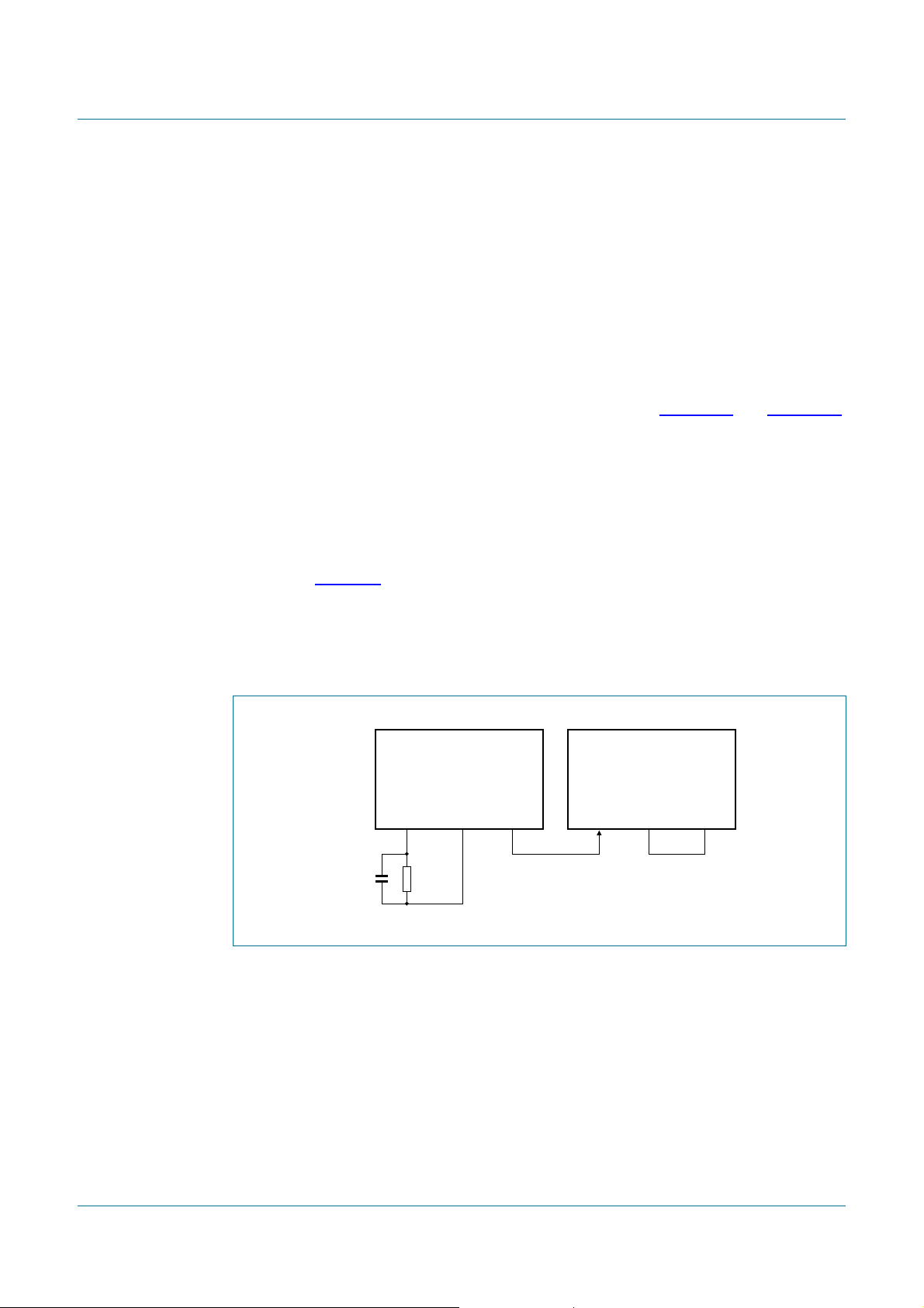
14.6 Device synchronization
If two or more TDA8932B devices are used in one application it is recommended that all
devices are synchronized running at the same switching frequency to avoid beat tones.
Synchronization canbe realized byconnecting all OSCIO pins together andconfigure one
of the TDA8932B devicesas master,while the other TDA8932B devices are configured as
slaves (see Figure 11).
A device is configured as master when connecting a resistor between pins OSCREF and
V
SSD(HW)
oscillator output for synchronization. The OSCREF pins of the slave devices should be
shorted to V
setting the carrier frequency. Pin OSCIO of the master is then configured as an
SSD(HW)
configuring pin OSCIO as an input.
(9)
master slave
C
osc
100 nF
TDA8932B
OSCREF V
R
osc
39 kΩ
IC1
SSD(HW)
OSCIO
OSCIO OSCREF
IC2
TDA8932B
V
SSD(HW)
001aaf600
Fig 11. Master slave concept in two chip application
14.7 Thermal behavior (printed-circuit board considerations)
The TDA8932B is available in two different thermally enhanced packages:
TDA8932BT in a SO32 (SOT287-1) package for reflow and wave solder process
TDA8932BTW in an HTSSOP32 (SOT549-1) package for reflow solder process only
The SO32 package has special thermal corner-leads, increasing the power capability
(reducing the overall R
and 32) should be attached to a copper plane. The SO package is very suitable for
applications with limited space for a thermal plane (in a single layer PCB design).
. To benefit from the corner leads pins V
th(j-a)
SSD(HW)
(pins 1, 16, 17
TDA8932B_3 © NXP B.V. 21 June 2007. All rights reserved.
Product data sheet Rev. 03— 21 June 2007 26 of 48
Page 27

NXP Semiconductors
The HTSSOP32 package has an exposed die-pad that reduces significantly the overall
R
th(j-a)
plane forcooling. The HTSSOP package will havea low thermal resistance when used on
a multi-layer PCB with sufficient space for one or two thermal planes.
Increasing the area of the thermal plane, the number of planes or the copper thickness
can reduce further the thermal resistance R
. Therefore it is required to solder the exposed die-pad (at V
of both packages.
th(j-a)
TDA8932B
Class-D audio amplifier
level) to a copper
SSD
Typical thermal resistance R
application board (55 mm × 45 mm), 35 µm copper, FR4 base material is 44 K/W.
Typical thermal resistance R
application board (55 mm × 40 mm), 35 µm copper, FR4 base material is 48 K/W.
Equation 10 shows the relation between the maximum allowable power dissipation P and
the thermal resistance from junction to ambient.
R
th j a–()
T
=
------------------------------------
–
j max()Tamb
P
Where:
R
= thermal resistance from junction to ambient
th(j-a)
T
= maximum junction temperature
j(max)
T
= ambient temperature
amb
P = power dissipation which is determined by the efficiency of the TDA8932B
The power dissipation is shown in Figure 22 (SE) and Figure 34 (BTL).
The thermal foldback will limit the maximum junction temperature to 140 °C.
14.8 Pumping effects
of the SO32 package soldered at a small 2-layer
th(j-a)
of the HTSSOP32 package soldered at a small 2-layer
th(j-a)
(10)
When the amplifier is used in a SE configuration, a so-called 'pumping effect' can occur.
During one switching interval, energy is taken from one supply (e.g. V
that energy is delivered back to the other supply line (e.g. V
) and visa versa. When
SSP1
), whilea part of
DDP1
the power supply cannot sink energy, the voltage across the output capacitors of that
power supply will increase.
The voltage increase caused by the pumping effect depends on:
• Speaker impedance
• Supply voltage
• Audio signal frequency
• Value of decoupling capacitors on supply lines
• Source and sink currents of other channels
The pumping effect should not cause a malfunction of either the audio amplifier and/or the
power supply. For instance, this malfunction can be caused by triggering of the
undervoltage or overvoltage protection of the amplifier.
Pumping effects in a SE configuration can be minimized by connecting audio inputs in
anti-phase and change the polarity of one speaker. This is illustrated in Figure 12.
TDA8932B_3 © NXP B.V. 21 June 2007. All rights reserved.
Product data sheet Rev. 03— 21 June 2007 27 of 48
Page 28
NXP Semiconductors
TDA8932B
Class-D audio amplifier
IN1P
audio
in1
audio
in2
IN1N
IN2N
IN2P
Fig 12. SE application for reducing pumping effects
OUT1
OUT2
001aad763
TDA8932B_3 © NXP B.V. 21 June 2007. All rights reserved.
Product data sheet Rev. 03— 21 June 2007 28 of 48
Page 29
NXP Semiconductors
14.9 SE curves measured in reference design
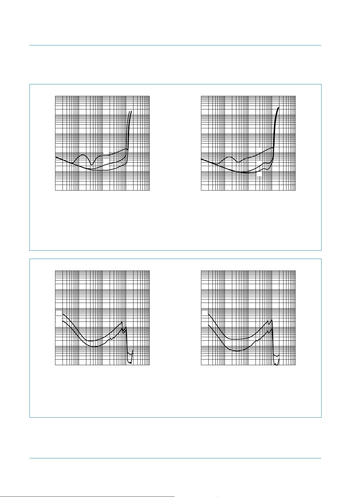
TDA8932B
Class-D audio amplifier
1010
001aad772
2
10
THD+N
(%)
10
1
−1
10
−2
10
−3
2
10
10
−2
10
−1
10
THD+N
(%)
10
10
10
2
10
1
−1
−2
−3
−2
10
−1
(1)
(2)
(3)
1
Po (W/channel)
a. VP=22V; RL=2× 4 Ω b. VP=30V; RL=2× 8 Ω
(1) fi= 6 kHz
(2) fi= 100 Hz
(3) fi= 1 kHz
Fig 13. Total harmonic distortion-plus-noise as a function of output power per channel
001aad773
(1)
(2)
(3)
2
1
1010
Po (W/channel)
10
10
001aad774
4
fi (Hz)
2
10
THD+N
(%)
10
1
(1)
(2)
−1
10
−2
10
−3
5
10
10 10
2
10
2
10
THD+N
(%)
10
1
(1)
(2)
−1
10
−2
10
−3
10
10 10
2
10
3
10
a. VP=22V; RL=2× 4 Ω b. VP=30V; RL=2× 8 Ω
(1) Po=10W
(2) Po=1W
Fig 14. Total harmonic distortion-plus-noise as a function of frequency
001aad775
3
10
4
10
fi (Hz)
5
TDA8932B_3 © NXP B.V. 21 June 2007. All rights reserved.
Product data sheet Rev. 03— 21 June 2007 29 of 48
Page 30
NXP Semiconductors
TDA8932B
Class-D audio amplifier
10
001aad777
4
(Hz)
f
i
5
40
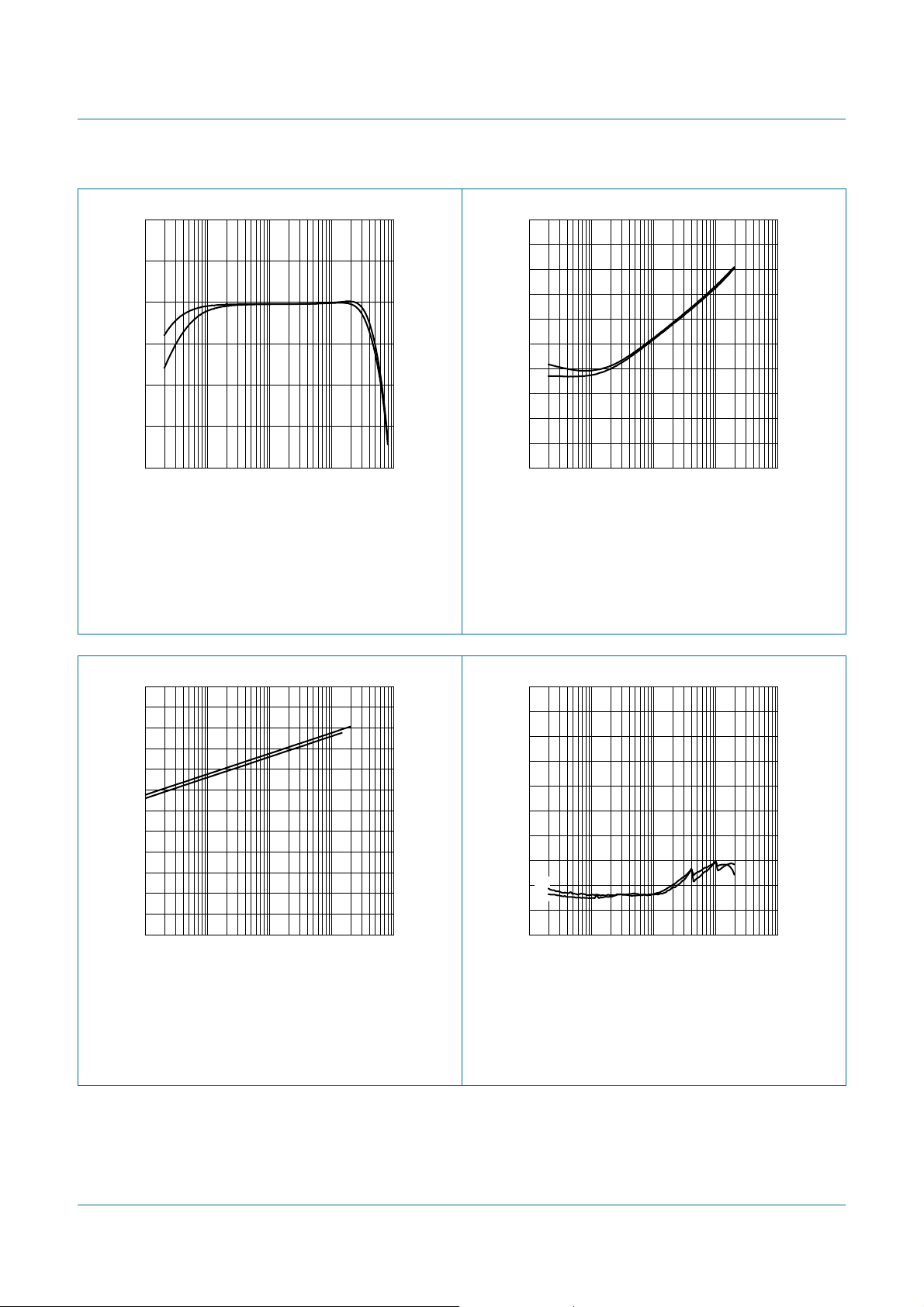
G
v
(dB)
30
(1)
(2)
20
10
10 10
2
10
3
10
10
Vi= 100 mV (RMS); Ri=0Ω; Cse = 1000 µF
(1) VP= 30 V; RL=2× 8 Ω
(2) VP= 22 V; RL=2× 4 Ω
001aad776
4
f
(Hz)
i
0
SVRR
(dB)
−20
−40
(1)
−60
(2)
−80
5
−100
10 10
V
ripple
2
10
3
10
= 500 mV (RMS) referenced to ground;
Ri=0Ω (shorted input)
(1) VP=30V; RL=2× 8 Ω
(2) VP=22V; RL=2× 4 Ω
Fig 15. Gain as a function of frequency Fig 16. Supply voltage ripple rejection as a function of
frequency
001aad778
(2)
(1)
1010
Po (W/channel)
10
2
S/N
(dB)
120
80
40
0
−2
10
−1
1
Ri=0Ω; 20 kHz brick-wall filter AES17
(1) VP= 22 V; RL=2× 4 Ω
(2) VP= 30 V; RL=2× 8 Ω
Fig 17. Signal-to-noise ratio as a function of output
power per channel
10
001aad779
4
f
(Hz)
i
5
0
α
cs
(dB)
−20
−40
−60
(1)
−80
(2)
−100
10 10
Po= 1 W; C
2
10
HVPREF
3
10
=47µF
(1) VP=22V; RL=2× 4 Ω
(2) VP=30V; RL=2× 8 Ω
Fig 18. Channel separation as a function of frequency
TDA8932B_3 © NXP B.V. 21 June 2007. All rights reserved.
Product data sheet Rev. 03— 21 June 2007 30 of 48
Page 31
NXP Semiconductors
TDA8932B
Class-D audio amplifier
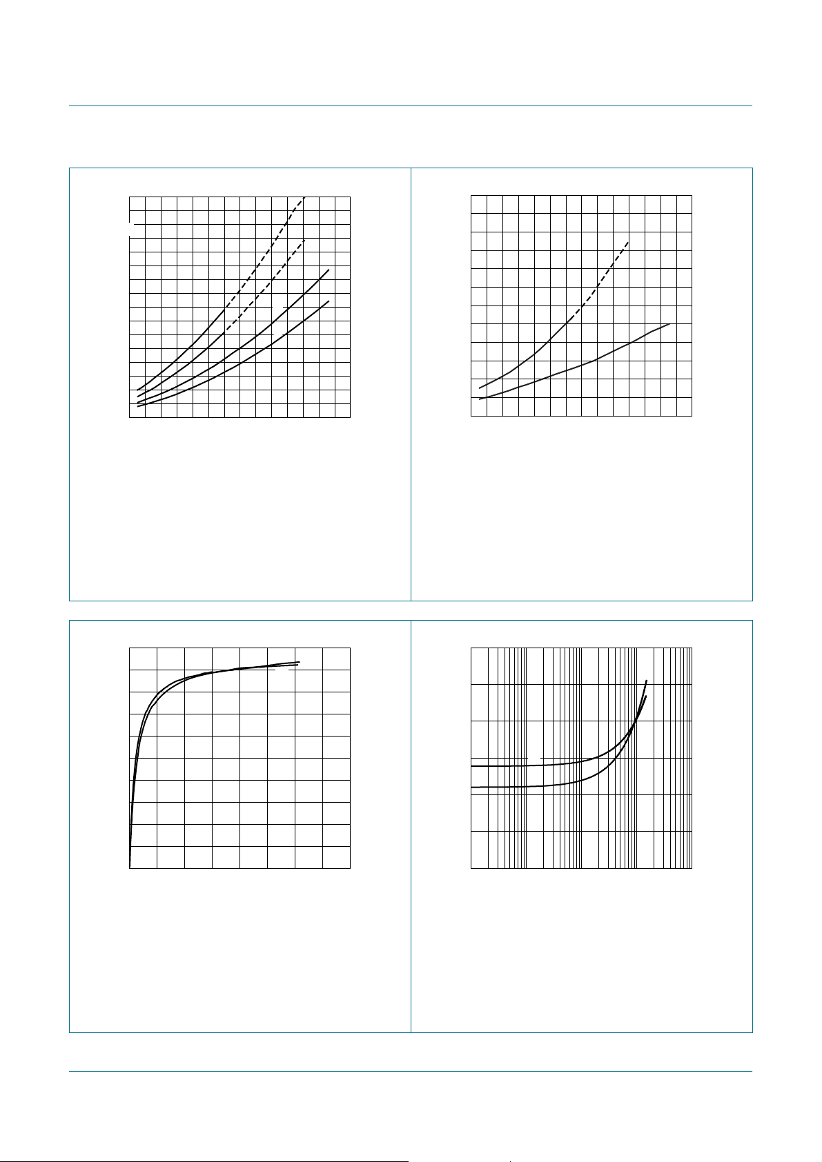
32
P
o
(W/channel)
24
16
8
0
10 3830 3414 18 22 26
001aaf886
(1)
(2)
(3)
(4)
VP (V)
fi= 1 kHz (short time PO); dashed line will require
heat sink for continuous time output power
(1) RL=2× 4 Ω; THD+N = 10 %
(2) RL=2× 4 Ω; THD+N = 0.5 %
(3) RL=2× 8 Ω; THD+N = 10 %
(4) RL=2× 8 Ω; THD+N = 0.5 %
Fig 19. Output power per channel as a function of
supply voltage
6
P
(W)
4
2
0
10 383414 18 22 26 30
(1)
(2)
001aaf889
VP (V)
fi= 1 kHz; power dissipation in junction only; short
time Po at THD+N = 10 %; dashed line will require
heat sink for continuous time output power
(1) RL=2× 4 Ω
(2) RL=2× 8 Ω
Fig 20. Power dissipation as a function of supply
voltage
100
η
po
(%)
80
60
40
20
0
02015510
(1) V
fi= 1 kHz;
P
η
=
------------------------ -
PO
2P
= 22 V; RL=2× 4 Ω
2P
×
o
o
p+×
001aad780
(2)
(1)
Po (W/channel)
(2) VP= 30 V; RL=2× 8 Ω
Fig 21. Output power efficiency as a function of output
power per channel
001aad781
1010
P
(W/channel)
o
2
10
P
(W)
3.0
2.0
1.0
(2)
(1)
0
−2
10
−1
1
fi= 1 kHz; power dissipation in junction only
(1) VP=22V; RL=2× 4 Ω
(2) VP=30V; RL=2× 8 Ω
Fig 22. Powerdissipation as a function of output power
per channel (two channels driven)
TDA8932B_3 © NXP B.V. 21 June 2007. All rights reserved.
Product data sheet Rev. 03— 21 June 2007 31 of 48
Page 32

NXP Semiconductors
TDA8932B
Class-D audio amplifier
32
P
o
(W/channel)
24
16
8
0
(3)
(2)
(1)
0 600480240 360120
001aaf887
t (s)
a. RL=2× 4 Ω; fi= 1 kHz; 2 layer SO32 application
board (55 mm × 45 mm) without heat sink
(1) VP=22V
(2) VP=26V
(3) VP=29V
Fig 23. Output power per channel as a function of time
32
P
o
(W/channel)
24
16
8
0
(2)
(1)
0 600480240 360120
001aaf888
t (s)
b. RL=2× 8 Ω; fi= 1 kHz; 2 layer SO32 application
board (55 mm × 45 mm) without heat sink
(1) VP=30V
(2) VP=34V
4
V
o
(V)
3
2
1
0
sleep
03210.5 2.51.5
Vi= 100 mV (RMS value); fi= 1 kHz; V
operating
001aaf890
V
POWERUP
ENGAGE
(V)
>3V Vi= 100 mV (RMS value); fi= 1 kHz;
Fig 24. Output voltage as a function of voltage on pin
POWERUP
4
V
o
(V)
3
2
1
0
V
mute
03210.5 2.51.5
POWERUP
>2V
001aaf891
operating
V
ENGAGE
(V)
Fig 25. Output voltage as a function of voltage on pin
ENGAGE
TDA8932B_3 © NXP B.V. 21 June 2007. All rights reserved.
Product data sheet Rev. 03— 21 June 2007 32 of 48
Page 33

NXP Semiconductors
14.10 BTL curves measured in reference design
TDA8932B
Class-D audio amplifier
1010
001aad782
Po (W)
2
10
THD+N
(%)
10
1
−1
10
−2
10
−3
2
10
10
−2
10
10
THD+N
(%)
10
10
10
10
2
1
−1
−2
−3
−2
10
−1
(1)
(2)
(3)
1
a. VP=12V; RL=4Ω b. VP=22V; RL=8Ω
(1) fi= 6 kHz
(2) fi= 1 kHz
(3) fi= 100 Hz
Fig 26. Total harmonic distortion-plus-noise as a function of output power
001aad783
(1)
(2)
(3)
−1
1
1010
Po (W)
2
10
10
001aae114
4
fi (Hz)
2
10
THD+N
(%)
10
1
−1
10
−2
10
−3
5
10
10 10
2
10
THD+N
(%)
10
1
−1
10
(1)
−2
10
−3
10
10 10
(2)
2
10
3
10
a. VP=12V; RL=4Ω b. VP=22V; RL=8Ω
(1) Po=10W
(2) Po=1W
Fig 27. Total harmonic distortion-plus-noise as a function of frequency
001aae115
(1)
(2)
2
10
3
10
4
10
fi (Hz)
5
TDA8932B_3 © NXP B.V. 21 June 2007. All rights reserved.
Product data sheet Rev. 03— 21 June 2007 33 of 48
Page 34

NXP Semiconductors
TDA8932B
Class-D audio amplifier
40
G
v
(dB)
30
20
10
10 10
2
10
3
10
10
Vi= 100 mV (RMS); Ri=0Ω
(1) VP= 12 V; RL=4Ω
(2) VP= 22 V; RL=8Ω
001aae116
4
f
(Hz)
i
0
SVRR
(dB)
(1)(2)
5
−20
−40
−60
−80
−100
10 10
V
ripple
2
10
3
10
= 500 mV (RMS) referenced to ground;
Ri=0Ω (shorted input)
(1) VP=22V; RL=8Ω
001aae117
(1)
(2)
(Hz)
i
5
4
10
f
(2) VP=12V; RL=4Ω
Fig 28. Gain as a function of frequency Fig 29. Supply voltage ripple rejection as a function of
frequency
1010
001aae118
Po (W)
2
10
S/N
(dB)
120
80
40
(2)
(1)
0
−2
10
−1
1
Ri=0Ω; 20 kHz brick-wall filter AES17
(1) RL=4Ω; VP=12V
(2) RL=8Ω; VP=22V
Fig 30. Signal-to-noise ratio as a function of output
power
70
P
o
(W)
60
50
40
30
20
10
0
10 34261814 3022
(3)
(1)
(2)
(4)
001aaf893
VP (V)
fi= 1 kHz (short time PO); dashed line will require
heat sink for continuous time output power
(1) RL=4Ω; THD+N = 10 %
(2) RL=4Ω; THD+N = 0.5 %
(3) RL=8Ω; THD+N = 10 %
(4) RL=8Ω; THD+N = 0.5 %
Fig 31. Output power as a function of supply voltage
TDA8932B_3 © NXP B.V. 21 June 2007. All rights reserved.
Product data sheet Rev. 03— 21 June 2007 34 of 48
Page 35

NXP Semiconductors
TDA8932B
Class-D audio amplifier
001aaf896
P
(W)
32
o
24
16
8
0
0 600480240 360120
(3)
(2)
(1)
a. RL=4Ω; fi= 1 kHz; 2 layer SO32 application
board (55 mm × 45 mm) without heat sink
(1) VP=12V
(2) VP= 13.5 V
(3) VP=15V
Fig 32. Output power as a function of time
t (s)
001aaf899
t (s)
P
(W)
60
o
50
40
30
20
10
(3)
0
0 600480240 360120
(2)
(1)
b. RL=8Ω; fi= 1 kHz; 2 layer SO32 application
board (55 mm × 45 mm) without heat sink
(1) VP=22V
(2) VP=26V
(3) VP=29V
100
η
po
(%)
80
60
40
20
0
0302010
fi= 1 kHz;
(1) V
= 12 V; RL=4Ω
P
(1)
(2)
P
η
PO
o
=
--------------------
Pop+()
001aae119
Po (W)
(2) VP= 22 V; RL=8Ω
Fig 33. Output power efficiency as a function of output
power
1010
001aae120
P
(W)
o
2
10
P
(W)
3.0
2.0
1.0
(2)
(1)
0
−2
10
−1
1
fi= 1 kHz; power dissipation in junction only
(1) VP=12V; RL=4Ω
(2) VP=22V; RL=8Ω
Fig 34. Power dissipation as a function of output power
TDA8932B_3 © NXP B.V. 21 June 2007. All rights reserved.
Product data sheet Rev. 03— 21 June 2007 35 of 48
Page 36

NXP Semiconductors
TDA8932B
Class-D audio amplifier
6
P
(W)
4
2
0
10 34261814 3022
fi= 1 kHz; power dissipation in junction only; short time Po at THD+N = 10 %; dashed line will require heat sink for
continuous time output power
(1) RL=4Ω
(2) RL= 8 Ω
(1)
Fig 35. Power dissipation as a function of supply voltage
001aaf904
(2)
VP (V)
TDA8932B_3 © NXP B.V. 21 June 2007. All rights reserved.
Product data sheet Rev. 03— 21 June 2007 36 of 48
Page 37

NXP Semiconductors
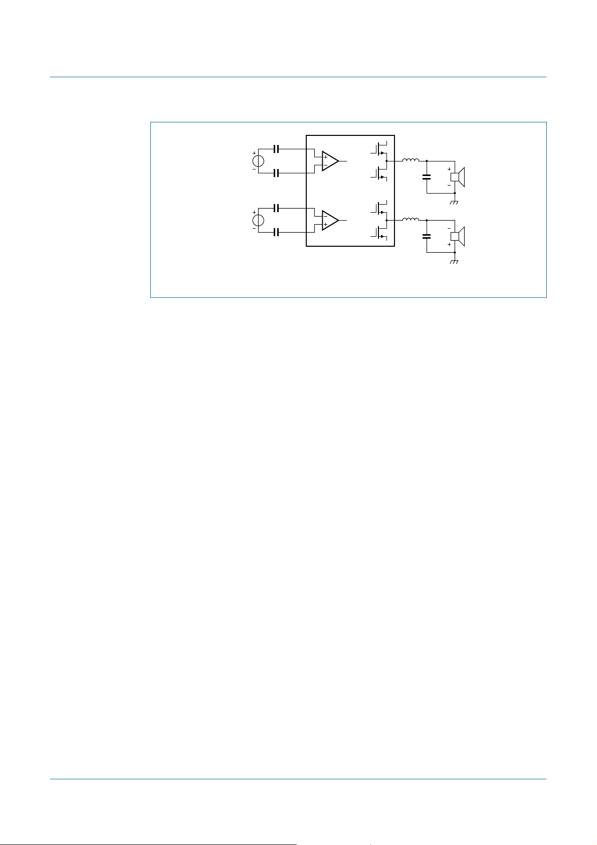
14.11 Typical application schematics (simplified)
VP VPA
GND
Rvdda
10 Ω
Cvdda
100 nF
Cvddp
220 µF
(35 V)
TDA8932B
Class-D audio amplifier
VP
MUTE control
SLEEP control
Chvpref
47 µF (25 V)
Cin
470 nF
Cosc
100 nF
Rosc
39 kΩ
Cin
470 nF
Cen
470 nF
Chvp
100 nF
V
SSD(HW)
Cin
470 nF
ENGAGE BOOT1
POWERUP OUT1
VPA
OSCREF
HVPREF OUT2
Cinref
100 nF
Cin
470 nF
V
SSD(HW)
1
IN1P
2
IN1N HVP1
3
DIAG
4
5
6
CGND
7
V
DDA
8
V
SSA
TDA8932B
9
U1
10
11
INREF
12
TEST
13
IN2N HVP2
14
IN2P DREF
15
16
32
31
30
29
28
27
26
25
24
23
22
21
20
19
18
17
V
SSD(HW)
OSCIO
V
DDP1
V
SSP1
STAB1
STAB2
V
SSP2
BOOT2
V
DDP2
V
SSD(HW)
Cbo
15
nF
Cbo
15
nF
Fig 36. Typical simplified application diagram for 2 × SE (asymmetrical supply)
Cstab
100 nF
VP
Cvddp
100 nF
Cdref
100 nF
VP
Cvddp
100 nF
Llc
Rsn
10 Ω
Csn
470 pF
Llc
Rsn
10 Ω
Csn
470 pF
Chvp
100 nF
Chvp
100 nF
Clc
Clc
Cse
Cse
001aaf601
TDA8932B_3 © NXP B.V. 21 June 2007. All rights reserved.
Product data sheet Rev. 03— 21 June 2007 37 of 48
Page 38

NXP Semiconductors
VP VPA
GND
Rvdda
10 Ω
Cvdda
100 nF
Cvddp
220 µF
(35 V)
TDA8932B
Class-D audio amplifier
VP
Cin
1 µF
Cin
1 µF
MUTE
control
SLEEP
control
Cosc
100 nF
Rosc
39 kΩ
Cen
470 nF
Chvp
100 nF
V
SSD(HW)
ENGAGE BOOT1
POWERUP OUT1
VPA
OSCREF
HVPREF OUT2
Cinref
100 nF
V
SSD(HW)
1
IN1P
2
IN1N HVP1
3
DIAG
4
5
6
CGND
7
V
DDA
8
V
SSA
TDA8932B
9
U1
10
11
INREF
12
TEST
13
IN2N HVP2
14
IN2P DREF
15
16
32
31
30
29
28
27
26
25
24
23
22
21
20
19
18
17
V
SSD(HW)
OSCIO
V
DDP1
V
SSP1
STAB1
STAB2
V
SSP2
BOOT2
V
DDP2
V
SSD(HW)
Cbo
15 nF
Cbo
15 nF
Fig 37. Typical simplified application diagram for 1 × BTL (asymmetrical supply)
Rhvp
470 Ω
Cstab
100 nF
VP
Cvddp
100 nF
Cdref
100 nF
Rhvp
470 Ω
VP
Cvddp
100 nF
Rsn
10 Ω
Csn
470 pF
Rsn
10 Ω
Csn
470 pF
Chvp
100 nF
Chvp
100 nF
Llc
Clc
Clc
Llc
001aaf602
TDA8932B_3 © NXP B.V. 21 June 2007. All rights reserved.
Product data sheet Rev. 03— 21 June 2007 38 of 48
Page 39

NXP Semiconductors
VDD VDDA
GND
VSS VSSA
Rvdda
10 Ω
Rvssa
10 Ω
Cvdda
100 nF
Cvssa
100 nF
Cvddp
220 µF
(25 V)
Cvssp
220 µF
(25 V)
TDA8932B
Class-D audio amplifier
VDD
VSS
MUTE control
SLEEP control
VSSA
Cin
470 nF
Cosc
100 nF
Rosc
39 kΩ
Cin
470 nF
Cen
470 nF
V
SSD(HW)
VSSA
Cin
470 nF
ENGAGE BOOT1
POWERUP OUT1
VDDA
VSSA
OSCREF
HVPREF OUT2
Cinref
100 nF
Cin
470 nF
V
SSD(HW)
VSSA
1
IN1P
2
IN1N HVP1
3
DIAG
4
5
6
CGND
7
V
DDA
8
V
SSA
TDA8932B
9
U1
10
11
INREF
12
TEST
13
IN2N HVP2
14
IN2P DREF
15
16
32
31
30
29
28
27
26
25
24
23
22
21
20
19
18
17
V
SSD(HW)
OSCIO
V
DDP1
V
SSP1
STAB1
STAB2
V
SSP2
BOOT2
V
DDP2
V
SSD(HW)
Cbo
15 nF
Cstab
100 nF
Cbo
15 nF
Cdref
100 nF
VSS
Cvssp
100 nF
VSS
VDD
Cvddp
100 nF
Cvssp
100 nF
VSSA
VDD
VSSA
Cvddp
100 nF
Llc
Rsn
10 Ω
Csn
470 pF
Llc
Rsn
10 Ω
Csn
470 pF
Clc
Clc
001aaf603
Fig 38. Typical simplified application diagram for 2 × SE (symmetrical supply)
TDA8932B_3 © NXP B.V. 21 June 2007. All rights reserved.
Product data sheet Rev. 03— 21 June 2007 39 of 48
Page 40

NXP Semiconductors
VDD VDDA
GND
VSS
Rvdda
10 Ω
Rvssa
10 Ω
Cvdda
100 nF
Cvssa
100 nF
VSSA
Cvddp
220 µF
(25 V)
Cvssp
220 µF
(25 V)
TDA8932B
Class-D audio amplifier
VDD
VSS
Cin
1 µF
Cin
1 µF
VSSA
MUTE
control
SLEEP
control
Cosc
100 nF
Rosc
39 kΩ
Cen
470 nF
V
SSD(HW)
VSSA
ENGAGE BOOT1
POWERUP OUT1
VDDA
VSSA
OSCREF
HVPREF OUT2
Cinref
100 nF
V
SSD(HW)
VSSA
1
IN1P
2
IN1N HVP1
3
DIAG
4
5
6
CGND
7
V
DDA
8
V
SSA
TDA8932B
9
U1
10
11
INREF
12
TEST
13
IN2N HVP2
14
IN2P DREF
15
16
32
31
30
29
28
27
26
25
24
23
22
21
20
19
18
17
V
SSD(HW)
OSCIO
V
DDP1
V
SSP1
STAB1
STAB2
V
SSP2
BOOT2
V
DDP2
V
SSD(HW)
Cbo
15 nF
Cstab
100 nF
Cbo
15 nF
Cdref
100 nF
VSS
Cvssp
100 nF
VSS
VDD
Cvddp
100 nF
Cvssp
100 nF
VDD
VSSA
Cvddp
100 nF
Llc
Rsn
10 Ω
Csn
470 pF
Llc
Rsn
10 Ω
Csn
470 pF
VSSA
Clc
Clc
001aaf606
Fig 39. Typical simplified application diagram for 1 × BTL (symmetrical supply)
15. Test information
15.1 Quality information
The
General Quality Specification for Integrated Circuits, SNW-FQ-611
TDA8932B_3 © NXP B.V. 21 June 2007. All rights reserved.
Product data sheet Rev. 03— 21 June 2007 40 of 48
is applicable.
Page 41

NXP Semiconductors
16. Package outline
TDA8932B
Class-D audio amplifier
SO32: plastic small outline package; 32 leads; body width 7.5 mm
D
c
y
Z
32
pin 1 index
1
e
17
16
w M
b
p
SOT287-1
E
H
E
A
2
A
1
detail X
A
X
v M
A
Q
(A )
L
p
L
A
3
θ
0 5 10 mm
scale
DIMENSIONS (inch dimensions are derived from the original mm dimensions)
UNIT
inches
Note
1. Plastic or metal protrusions of 0.15 mm (0.006 inch) maximum per side are not included.
A
A1A2A3b
max.
0.3
mm
2.65
0.1
OUTLINE
VERSION
SOT287-1 MO-119
0.1
0.012
0.004
2.45
0.25
2.25
0.096
0.01
0.089
IEC JEDEC JEITA
0.49
0.36
0.02
0.01
p
0.27
0.18
0.011
0.007
(1)E(1)
cD
20.7
20.3
0.81
0.80
REFERENCES
eHELLpQZywv θ
7.6
7.4
0.30
0.29
1.27
0.05
10.65
10.00
0.419
0.394
1.4
0.055
1.1
0.4
0.043
0.016
1.2
1.0
0.047
0.039
0.25 0.1
0.25
0.010.01
EUROPEAN
PROJECTION
0.004
ISSUE DATE
(1)
0.95
0.55
0.037
0.022
00-08-17
03-02-19
o
8
o
0
Fig 40. Package outline SOT287-1 (SO32)
TDA8932B_3 © NXP B.V. 21 June 2007. All rights reserved.
Product data sheet Rev. 03— 21 June 2007 41 of 48
Page 42
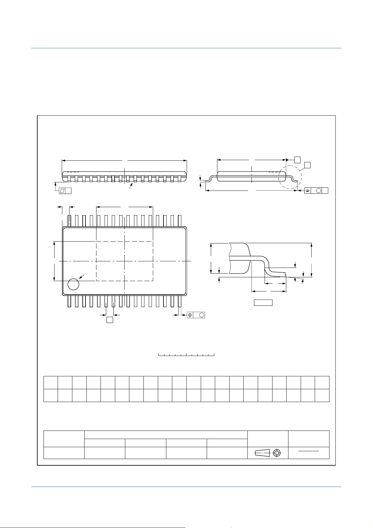
NXP Semiconductors
HTSSOP32: plastic thermal enhanced thin shrink small outline package; 32 leads;
body width 6.1 mm; lead pitch 0.65 mm; exposed die pad
TDA8932B
Class-D audio amplifier
SOT549-1
D
c
y
Z
32
E
h
pin 1 index
1
exposed die pad side
D
h
e
17
A
2
A
1
16
w M
b
p
E
H
E
detail X
L
p
L
(A3)
A
X
v M
A
A
θ
E
6.2
6.0
(2)
2.5
scale
5 mm
eHELL
E
h
3.6
3.4
8.3
0.65 1 0.2
7.9
p
0.75
0.50
EUROPEAN
PROJECTION
0.1
Zywv θ
0.78
0.1
0.48
ISSUE DATE
03-04-07
05-11-02
o
8
o
0
0
DIMENSIONS (mm are the original dimensions).
A
UNIT A1A2A3b
max.
0.95
1.1
0.15
0.05
0.85
IEC JEDEC JEITA
mm
Notes
1. Plastic or metal protrusions of 0.15 mm maximum per side are not included.
2. Plastic interlead protrusions of 0.25 mm maximum per side are not included.
OUTLINE
VERSION
SOT549-1
0.25
p
0.30
0.19
cD
0.20
11.1
0.09
10.9
MO-153
(1)
D
h
5.1
4.9
REFERENCES
Fig 41. Package outline SOT549-1 (HTSSOP32)
TDA8932B_3 © NXP B.V. 21 June 2007. All rights reserved.
Product data sheet Rev. 03— 21 June 2007 42 of 48
Page 43

NXP Semiconductors
17. Soldering
This text provides a very brief insight into a complex technology. A more in-depth account
of soldering ICs can be found in Application Note
soldering description”
17.1 Introduction to soldering
Soldering is one of the most common methods through which packages are attached to
Printed Circuit Boards (PCBs), to form electrical circuits. The soldered joint provides both
the mechanical and the electrical connection. There is no single soldering method that is
ideal for all IC packages. Wave soldering is often preferred when through-hole and
Surface Mount Devices (SMDs) are mixed on one printed wiring board; however, it is not
suitable for fine pitch SMDs. Reflow soldering is ideal for the small pitches and high
densities that come with increased miniaturization.
17.2 Wave and reflow soldering
Wave soldering is a joining technology in which the joints are made by solder coming from
a standing wave of liquid solder. The wave soldering process is suitable for the following:
TDA8932B
Class-D audio amplifier
AN10365 “Surface mount reflow
.
• Through-hole components
• Leaded or leadless SMDs, which are glued to the surface of the printed circuit board
Not all SMDs can be wave soldered. Packages with solder balls, and some leadless
packages which have solder lands underneath the body, cannot be wave soldered. Also,
leaded SMDs with leads having a pitch smaller than ~0.6 mm cannot be wave soldered,
due to an increased probability of bridging.
The reflow soldering process involves applying solder paste to a board, followed by
component placement and exposure to a temperature profile. Leaded packages,
packages with solder balls, and leadless packages are all reflow solderable.
Key characteristics in both wave and reflow soldering are:
• Board specifications, including the board finish, solder masks and vias
• Package footprints, including solder thieves and orientation
• The moisture sensitivity level of the packages
• Package placement
• Inspection and repair
• Lead-free soldering versus PbSn soldering
17.3 Wave soldering
Key characteristics in wave soldering are:
• Process issues, such as application of adhesive and flux, clinching of leads, board
transport, the solder wave parameters, and the time during which components are
exposed to the wave
• Solder bath specifications, including temperature and impurities
TDA8932B_3 © NXP B.V. 21 June 2007. All rights reserved.
Product data sheet Rev. 03— 21 June 2007 43 of 48
Page 44

NXP Semiconductors
17.4 Reflow soldering
Key characteristics in reflow soldering are:
• Lead-free versus SnPb soldering; note thata lead-free reflowprocess usually leads to
• Solder paste printing issues including smearing, release, and adjusting the process
• Reflow temperature profile; this profile includes preheat, reflow (in which the board is
Table 16. SnPb eutectic process (from J-STD-020C)
Package thickness (mm) Package reflow temperature (°C)
< 2.5 235 220
≥ 2.5 220 220
TDA8932B
Class-D audio amplifier
higher minimum peak temperatures (see Figure 42) than a PbSn process, thus
reducing the process window
window for a mix of large and small components on one board
heated to the peak temperature) and cooling down. It is imperative that the peak
temperature is high enough for the solder to makereliable solder joints (a solder paste
characteristic). In addition, the peak temperature must be low enough that the
packages and/or boards are not damaged. The peak temperature of the package
depends on package thickness and volume and is classified in accordance with
Table 16 and 17
Volume (mm3)
< 350 ≥ 350
Table 17. Lead-free process (from J-STD-020C)
Package thickness (mm) Package reflow temperature (°C)
Volume (mm3)
< 350 350 to 2000 > 2000
< 1.6 260 260 260
1.6 to 2.5 260 250 245
> 2.5 250 245 245
Moisture sensitivity precautions, as indicated on the packing, must be respected at all
times.
Studies have shown that small packages reach higher temperatures during reflow
soldering, see Figure 42.
TDA8932B_3 © NXP B.V. 21 June 2007. All rights reserved.
Product data sheet Rev. 03— 21 June 2007 44 of 48
Page 45
NXP Semiconductors
Fig 42. Temperature profiles for large and small components
maximum peak temperature
temperature
MSL: Moisture Sensitivity Level
= MSL limit, damage level
minimum peak temperature
= minimum soldering temperature
TDA8932B
Class-D audio amplifier
peak
temperature
time
001aac844
For further information on temperature profiles, refer to Application Note
“Surface mount reflow soldering description”
18. Abbreviations
Table 18. Abbreviations
Acronym Description
BTL Bridge Tied Load
DMOS Double diffused Metal Oxide Semiconductor
ESD ElectroStatic Discharge
OCP OverCurrent Protection
OTP OverTemperature Protection
OVP OverVoltage Protection
PWM Pulse Width Modulation
SE Single-Ended
TF Thermal Foldback
UBP UnBalance Protection
UVP UnderVoltage Protection
WP Window Protection
AN10365
.
TDA8932B_3 © NXP B.V. 21 June 2007. All rights reserved.
Product data sheet Rev. 03— 21 June 2007 45 of 48
Page 46

NXP Semiconductors
TDA8932B
Class-D audio amplifier
19. Revision history
Table 19. Revision history
Document ID Release date Data sheet status Change notice Supersedes
TDA8932B_3 20070621 Product data sheet - TDA8932B_2
Modifications:
TDA8932B_2 20070329 Preliminary data sheet - TDA8932B_1
TDA8932B_1 20070214 Objective data sheet - -
• Status upgraded to Product data sheet
TDA8932B_3 © NXP B.V. 21 June 2007. All rights reserved.
Product data sheet Rev. 03 — 21 June 2007 46 of 48
Page 47

NXP Semiconductors
20. Legal information
20.1 Data sheet status
TDA8932B
Class-D audio amplifier
Document status
Objective [short] data sheet Development This document contains data from the objective specification for product development.
Preliminary [short] data sheet Qualification This document contains data from the preliminary specification.
Product [short] data sheet Production This document contains the product specification.
[1] Please consult the most recently issued document before initiating or completing a design.
[2] The term ‘short data sheet’ is explained in section “Definitions”.
[3] The product status of device(s) described in this documentmay have changed since this document was published and may differin case of multiple devices. The latest product status
information is available on the Internet at URL
[1][2]
Product status
20.2 Definitions
Draft — The document is a draft version only. The content is still under
internal review and subject to formal approval, which may result in
modifications or additions. NXP Semiconductors does not give any
representations or warranties as to the accuracy or completeness of
information included herein and shallhaveno liability for the consequences of
use of such information.
Short data sheet — A short data sheet is an extract from a full data sheet
with the same product typenumber(s)and title. A short data sheet is intended
for quick referenceonly and should not be relied upon to contain detailed and
full information. For detailed and full information see the relevant full data
sheet, which is available on request via the local NXP Semiconductors sales
office. In case of any inconsistency or conflict with the short data sheet, the
full data sheet shall prevail.
20.3 Disclaimers
General — Information in this document is believed to be accurate and
reliable. However,NXP Semiconductors does not give any representations or
warranties, expressedor implied, asto the accuracy or completeness of such
information and shall have no liability for the consequences of use of such
information.
Right to make changes — NXP Semiconductors reserves the right to make
changes to information published in this document, including without
limitation specifications and product descriptions, at any time and without
notice. This document supersedes and replaces all information supplied prior
to the publication hereof.
Suitability for use — NXP Semiconductors products are not designed,
authorized or warranted to be suitable for use in medical, military, aircraft,
space or life support equipment, nor in applications where failure or
[3]
http://www.nxp.com.
Definition
malfunction of aNXPSemiconductors product can reasonably be expectedto
result in personal injury, death or severe property or environmental damage.
NXP Semiconductors accepts no liability for inclusion and/or use of NXP
Semiconductors products in such equipment or applications and therefore
such inclusion and/or use is at the customer’s own risk.
Applications — Applications that are described herein for any of these
products are for illustrative purposes only. NXP Semiconductors makes no
representation or warranty that such applications will be suitable for the
specified use without further testing or modification.
Limiting values — Stress above one or more limiting values (as defined in
the Absolute Maximum Ratings System of IEC 60134) may cause permanent
damage to the device.Limiting valuesare stress ratings only and operation of
the device at these or any other conditions above those given in the
Characteristics sections of this document is not implied. Exposure to limiting
values for extended periods may affect device reliability.
Terms and conditions of sale — NXP Semiconductors products are sold
subject to the general terms and conditions of commercial sale, as published
at
http://www.nxp.com/profile/terms, including those pertaining to warranty,
intellectual property rights infringement and limitation of liability, unless
explicitly otherwise agreed to in writing by NXP Semiconductors. In case of
any inconsistency or conflict between information in this document and such
terms and conditions, the latter will prevail.
No offer to sell or license — Nothing in this document may be interpreted
or construed as an offer to sell products that is open for acceptance or the
grant, conveyanceor implication of any license under any copyrights, patents
or other industrial or intellectual property rights.
20.4 Trademarks
Notice: All referencedbrands, product names, service names and trademarks
are the property of their respective owners.
21. Contact information
For additional information, please visit: http://www.nxp.com
For sales office addresses, send an email to: salesaddresses@nxp.com
TDA8932B_3 © NXP B.V. 21 June 2007. All rights reserved.
Product data sheet Rev. 03 — 21 June 2007 47 of 48
Page 48

NXP Semiconductors
22. Contents
TDA8932B
Class-D audio amplifier
1 General description . . . . . . . . . . . . . . . . . . . . . . 1
2 Features . . . . . . . . . . . . . . . . . . . . . . . . . . . . . . . 1
3 Applications . . . . . . . . . . . . . . . . . . . . . . . . . . . . 1
4 Quick reference data . . . . . . . . . . . . . . . . . . . . . 2
5 Ordering information. . . . . . . . . . . . . . . . . . . . . 2
6 Block diagram . . . . . . . . . . . . . . . . . . . . . . . . . . 3
7 Pinning information. . . . . . . . . . . . . . . . . . . . . . 4
7.1 Pinning . . . . . . . . . . . . . . . . . . . . . . . . . . . . . . . 4
7.2 Pin description . . . . . . . . . . . . . . . . . . . . . . . . . 4
8 Functional description . . . . . . . . . . . . . . . . . . . 5
8.1 General. . . . . . . . . . . . . . . . . . . . . . . . . . . . . . . 5
8.2 Mode selection and interfacing. . . . . . . . . . . . . 6
8.3 Pulse width modulation frequency . . . . . . . . . . 7
8.4 Protection . . . . . . . . . . . . . . . . . . . . . . . . . . . . . 8
8.4.1 Thermal Foldback (TF). . . . . . . . . . . . . . . . . . . 9
8.4.2 OverTemperature Protection (OTP) . . . . . . . . . 9
8.4.3 OverCurrent Protection (OCP) . . . . . . . . . . . . . 9
8.4.4 Window Protection (WP). . . . . . . . . . . . . . . . . . 9
8.4.5 Supply voltage protection . . . . . . . . . . . . . . . . 10
8.5 Diagnostic input and output . . . . . . . . . . . . . . 11
8.6 Differential inputs . . . . . . . . . . . . . . . . . . . . . . 11
8.7 Output voltage buffers. . . . . . . . . . . . . . . . . . . 11
9 Internal circuitry. . . . . . . . . . . . . . . . . . . . . . . . 12
10 Limiting values. . . . . . . . . . . . . . . . . . . . . . . . . 16
11 Thermal characteristics. . . . . . . . . . . . . . . . . . 16
12 Static characteristics. . . . . . . . . . . . . . . . . . . . 17
13 Dynamic characteristics . . . . . . . . . . . . . . . . . 19
14 Application information. . . . . . . . . . . . . . . . . . 22
14.1 Output power estimation. . . . . . . . . . . . . . . . . 22
14.2 Output current limiting. . . . . . . . . . . . . . . . . . . 24
14.3 Speaker configuration and impedance. . . . . . 24
14.4 Single-ended capacitor. . . . . . . . . . . . . . . . . . 24
14.5 Gain reduction . . . . . . . . . . . . . . . . . . . . . . . . 25
14.6 Device synchronization. . . . . . . . . . . . . . . . . . 26
14.7 Thermal behavior (printed-circuit board
considerations) . . . . . . . . . . . . . . . . . . . . . . . . 26
14.8 Pumping effects . . . . . . . . . . . . . . . . . . . . . . . 27
14.9 SE curves measured in reference design. . . . 29
14.10 BTL curves measured in reference design. . . 33
14.11 Typical application schematics (simplified). . . 37
15 Test information. . . . . . . . . . . . . . . . . . . . . . . . 40
15.1 Quality information . . . . . . . . . . . . . . . . . . . . . 40
16 Package outline . . . . . . . . . . . . . . . . . . . . . . . . 41
17 Soldering . . . . . . . . . . . . . . . . . . . . . . . . . . . . . 43
17.1 Introduction to soldering. . . . . . . . . . . . . . . . . 43
17.2 Wave and reflow soldering. . . . . . . . . . . . . . . 43
17.3 Wave soldering. . . . . . . . . . . . . . . . . . . . . . . . 43
17.4 Reflow soldering. . . . . . . . . . . . . . . . . . . . . . . 44
18 Abbreviations . . . . . . . . . . . . . . . . . . . . . . . . . 45
19 Revision history . . . . . . . . . . . . . . . . . . . . . . . 46
20 Legal information . . . . . . . . . . . . . . . . . . . . . . 47
20.1 Data sheet status. . . . . . . . . . . . . . . . . . . . . . 47
20.2 Definitions . . . . . . . . . . . . . . . . . . . . . . . . . . . 47
20.3 Disclaimers. . . . . . . . . . . . . . . . . . . . . . . . . . . 47
20.4 Trademarks . . . . . . . . . . . . . . . . . . . . . . . . . . 47
21 Contact information . . . . . . . . . . . . . . . . . . . . 47
22 Contents. . . . . . . . . . . . . . . . . . . . . . . . . . . . . . 48
Please be aware that important notices concerning this document and the product(s)
described herein, have been included in section ‘Legal information’.
© NXP B.V. 21 June 2007. All rights reserved.
For more information, please visit: http://www.nxp.com
For sales office addresses, please send an email to: salesaddresses@nxp.com
Date of release: 21 June 2007
Document identifier: TDA8932B_3
 Loading...