

Page 1

QorIQ T2080 Reference Design Board
(T2080RDB-PC) User Guide
Document Number: T2080RDBPCUG
Rev. 0, 04/2016
Page 2

QorIQ T2080 Reference Design Board (T2080RDB-PC) User Guide, Rev. 0, 04/2016
2 Freescale Semiconductor, Inc.
Page 3

Contents
Section number Title Page
Chapter 1
Overview
1.1 Related documentation....................................................................................................................................................5
1.2 Acronyms and abbreviations...........................................................................................................................................6
1.3 T2080 silicon features.....................................................................................................................................................7
1.4 T2080RDB-PC board features........................................................................................................................................8
1.5 Block diagram.................................................................................................................................................................9
Chapter 2
Architecture
2.1 Processor.........................................................................................................................................................................13
2.2 Power.............................................................................................................................................................................. 13
2.3 Reset................................................................................................................................................................................15
2.4 Clocks............................................................................................................................................................................. 16
2.5 DDR................................................................................................................................................................................17
2.6 SerDes port......................................................................................................................................................................18
2.6.1 PCI Express support...........................................................................................................................................20
2.6.2 XFI 10G optics port support.............................................................................................................................. 20
2.6.3 XFI 10GBase-T port support............................................................................................................................. 21
2.6.4 SATA support.................................................................................................................................................... 21
2.7 Ethernet controllers ........................................................................................................................................................21
2.8 Ethernet Management Interface......................................................................................................................................22
2.9 I2C...................................................................................................................................................................................23
2.10 SPI interface ...................................................................................................................................................................24
2.11 Local bus.........................................................................................................................................................................25
2.12 SDHC interface...............................................................................................................................................................25
2.13 USB interface..................................................................................................................................................................26
2.14 RS-232............................................................................................................................................................................ 27
2.15 JTAG/COP port.............................................................................................................................................................. 28
QorIQ T2080 Reference Design Board (T2080RDB-PC) User Guide, Rev. 0, 04/2016
Freescale Semiconductor, Inc. 3
Page 4

Section number Title Page
2.16 Connectors, Headers, Jumper, Push buttons, and LEDs.................................................................................................30
2.16.1 Connectors......................................................................................................................................................... 30
2.16.2 Headers...............................................................................................................................................................31
2.16.3 Jumper................................................................................................................................................................ 31
2.16.4 Push buttons....................................................................................................................................................... 32
2.16.5 LEDs.................................................................................................................................................................. 32
2.17 Temperature.................................................................................................................................................................... 32
2.18 DIP switch definition......................................................................................................................................................33
Chapter 3
CPLD Specification
3.1 CPLD Memory Map....................................................................................................................................................... 37
3.1.1 Chip ID1 register (CHIPID1).............................................................................................................................37
3.1.2 Chip ID2 register (CHIPID2).............................................................................................................................38
3.1.3 Hardware version register (HWVER)................................................................................................................38
3.1.4 Software version register (SWVER)..................................................................................................................39
3.1.5 Reset control register (RSTCON)...................................................................................................................... 39
3.1.6 Flash control and status register (FLHCSR)...................................................................................................... 40
3.1.7 Thermal control and status register (THMCSR)................................................................................................40
3.1.8 Panel LED control and status register (LEDCSR).............................................................................................41
3.1.9 SFP+ control and status register (SFPCSR).......................................................................................................41
3.1.10 Miscellanies control and status register (MISCCSR)........................................................................................ 42
3.1.11 Boot configuration override register (BOOTOR).............................................................................................. 43
3.1.12 Boot configuration register 1 (BOOTCFG1)..................................................................................................... 43
3.1.13 Boot configuration register 2 (BOOTCFG2)..................................................................................................... 43
QorIQ T2080 Reference Design Board (T2080RDB-PC) User Guide, Rev. 0, 04/2016
4 Freescale Semiconductor, Inc.
Page 5

Chapter 1
Overview
The T2080RDB-PC is a high-performance computing evaluation, development, and test
platform supporting the T2080 QorIQ Power Architecture® processor. The T2080RDBPC is optimized to support the high-bandwidth DDR3LP memory and a full complement
of high-speed SerDes ports. This system has two working modes, the Standalone mode
and the PCIe Endpoint mode. The motherboard, inside the T2080RDB-PC, is a PCIe
form factor card and it is installed in a custom 1U chassis. The system will be in
standalone mode by default and you can remove the PCIe from its chassis for PCIe
Endpoint mode operation.
NOTE
The T2080RDB boards are using Freescale's C29x Crypto
Coprocessor series silicon.
1.1
Related documentation
The table below lists the related documentation:
Table 1-1. Related documentation
Document name Description
T2080 QorIQ
Integrated
Multicore
Communication
Processor Family
Reference Manual
T2080 Product
Brief
T2080 QorIQ
Advanced
Multicore
Processor Data
Sheet
This document provides a detail description on the T2080 QorIQ multicore processor and on some of its
features like memory map, serial interfaces, power supply, chip features, and clock information.
This document provides an overview of the Freescale T2080 features and examples of the T2080 usage.
This document contains the T2080 information on pin assignments, electrical characteristics, hardware
design, considerations, package information, and ordering information.
QorIQ T2080 Reference Design Board (T2080RDB-PC) User Guide, Rev. 0, 04/2016
Freescale Semiconductor, Inc. 5
Page 6

Acronyms and abbreviations
NOTE
Some of the documents mentioned above may be available only
under a non-disclosure agreement (NDA). To request access to
these documents, contact your local field applications engineer
or sales representative.
1.2 Acronyms and abbreviations
Table 1-2. Acronyms and abbreviations
Usage Description
COP Common On-chip Processor
CPC CoreNet Platform Cache
CPLD Complex Programmable Logic Device
DIMM Dual In-Line Memory Module
DIP Dual In-Line Package
DMA Direct Memory Access
DPAA Data Path Acceleration Architecture
DRAM Dynamic Random Access Memory
DUT Device Under Test
EC Ethernet Controllers
ECC Error Detection and Correction
EMI Ethernet Management Interfaces
eSDHC enhanced Secure Digital Host Controller
eSPI enhanced Serial Peripheral Interface
FPGA Field-Programmable Gate Array
HW Hardware
I2C Inter - Integrated Circuit
IFC Integrated Flash Controller
JTAG Joint Test Action Group
PCIe/PEX PCIe = PCI Express = PEX
PLD Programmable Logic Device
POR Power On Reset
QMan Queue Manager
SATA Serial Advanced Technology Attachment
SD Secure Digital
SerDes Serializer/Deserializer
SGMII Serial Gigabit Media Independent Interface
SPI Serial Peripheral Interface
SW Switch
SYSCLK System Clock
Table continues on the next page...
QorIQ T2080 Reference Design Board (T2080RDB-PC) User Guide, Rev. 0, 04/2016
6 Freescale Semiconductor, Inc.
Page 7

Chapter 1 Overview
Table 1-2. Acronyms and abbreviations (continued)
Usage Description
UART Universal Asynchronous Receiver/Transmitter
VCC Voltage for Circuit
VTT Voltage for Terminal
1.3 T2080 silicon features
The T2080 silicon features are as follows:
• Four e6500 cores, built on Power Architecture technology, sharing a 2 MB L2 cache
• 512 KB CoreNet Platform cache (CPC)
• Hierarchical interconnect fabric:
• CoreNet fabric supporting coherent and non-coherent transactions with
prioritization and bandwidth allocation amongst CoreNet endpoints
• Queue Manager (QMan) fabric supporting packet-level queue management and
quality of service scheduling
• One 32/64-bit DDR3 SDRAM memory controller:
• DDR3 and DDR3L with ECC and interleaving support
• Memory pre-fetch engine
• Data Path Acceleration Architecture (DPAA) incorporating acceleration for the
following functions:
• Packet parsing, classification, and distribution (Frame Manager 1.1)
• Queue management for scheduling, packet sequencing, and congestion
management (Queue Manager 1.1)
• Hardware buffer management for buffer allocation and de-allocation (Buffer
Manager 1.1)
• Cryptography Acceleration (SEC 5.2)
• RegEx Pattern Matching Acceleration (PME 2.1)
• Decompression/Compression Acceleration (DCE 1.0)
• DPAA chip-to-chip interconnect, using RapidIO Message Manager (RMan 1.0)
• 16 SerDes lanes at up to 10 GHz.
• Eight Ethernet interfaces, supporting combinations of:
• Up to four 10 Gbit/s Ethernet MACs
• Up to eight 1 Gbit/s Ethernet MACs
• Up to four 2.5 Gbit/s Ethernet MACs
• IEEE 1588 standard support.
• High-speed peripheral interfaces:
QorIQ T2080 Reference Design Board (T2080RDB-PC) User Guide, Rev. 0, 04/2016
Freescale Semiconductor, Inc. 7
Page 8

T2080RDB-PC board features
• Four PCI Express controllers (two supporting PCIe 2.0 and two supporting PCIe
3.0)
• Two Serial RapidIO 2.0 controllers running at up to 5 GHz with Type 11
messaging and Type 9 data streaming support
• Additional peripheral interfaces:
• Two Serial ATA (SATA 2.0) controllers
• Two high-speed USB 2.0 controllers with integrated PHY
• Enhanced secure digital host controller (SD/MMC/eMMC)
• Enhanced Serial peripheral interface (eSPI)
• Four I2C controllers
• Four 2-pin UARTs or two 4-pin UARTs
• Integrated flash controller supporting NAND and NOR flash
• Three 8-channel DMA engines
• 896 FC-PBGA package, 25 mm x 25 mm, 0.8 mm pitch
1.4
T2080RDB-PC board features
The T2080RDB-PC board features are as follows:
• SerDes connections
• 16 lanes configuration:
• SerDes-1 Lane A-B: to two 10GSFP+ (MAC9 and MAC10)
• SerDes-1 Lane C-D: to two 10GBase-T (MAC1 and MAC2)
• SerDes-1 Lane E-H: to PCIe slot (PCIe4 x4, Gen3)
• SerDes-2 Lane A-D: to PCIe Goldfinger (PCIe1 x4, Gen2)
• SerDes-2 Lane E-F: to C293 secure coprocessor (PCIe2 x2)
• SerDes-2 Lane G-H: to SATA1 and SATA2
• DDR controller
• Supports data rates of up to 1600 MHz or 1866 MHz
• Supports one DDR3LP DIMM of single, dual-rank types
• DDR power supplies 1.35 V to all devices with automatic tracking of VTT
• IFC/Local Bus
• NAND flash: 8 bit, async, up to 1 GB
• NOR: 16 bit, non-multiplexed, up to 128 MB, NOR devices support 8 virtual
banks
• Ethernet
• Two on-board RGMII 10/100/1G Ethernet ports
• Two on-board XFI 10GEDC for 10G SFP+ Port
• Two on-board XFI 10GBase-T port
QorIQ T2080 Reference Design Board (T2080RDB-PC) User Guide, Rev. 0, 04/2016
8 Freescale Semiconductor, Inc.
Page 9

Chapter 1 Overview
• CPLD
• Manages system power and reset sequencing
• Configures DUT, board, clock with dynamic
• Reset and interrupt monitor and control
• General fault monitoring and logging
• Clocks
• System and DDR clock (SYSCLK, DDRCLK)
• Switch selectable to one of the 16 common settings in the interval 64
MHz-166 MHz
• Software programmable in 1 MHz increments from 1-200 MHz
• SerDes clocks
• Provides clocks to all SerDes blocks and slots
• 100 MHz
• 156.25 MHz
• Power supplies
• Dedicated PMBus regulator for core power; adjustable from 0.7 V to 1.3 V at 60
A
• USB
• Supports two USB 2.0 ports with integrated PHYs: Two type A ports with 5 V
@ 1.5 A per port
• MicroSD card
• MicroSD port connects directly to MicroSD or TF
• SPI
• Onboard support of SPI flash
• Other I/O
• Two serial ports
• Two I2C ports
1.5
Block diagram
The T2080RDB-PC supports two modes of operation, the Standalone mode and the
Endpoint mode. There is one configuration in the Standalone mode and second
configurations is in the Endpoint mode, the major differences are in the PCIe support. All
configurations have Freescale C293, 4x XFI, 2x RGMII, DDR, NOR, NAND, SPI
EEPROM, I2C EEPROM, and GPIO. Muxing is controlled by FPGA/CPLD.
QorIQ T2080 Reference Design Board (T2080RDB-PC) User Guide, Rev. 0, 04/2016
Freescale Semiconductor, Inc. 9
Page 10
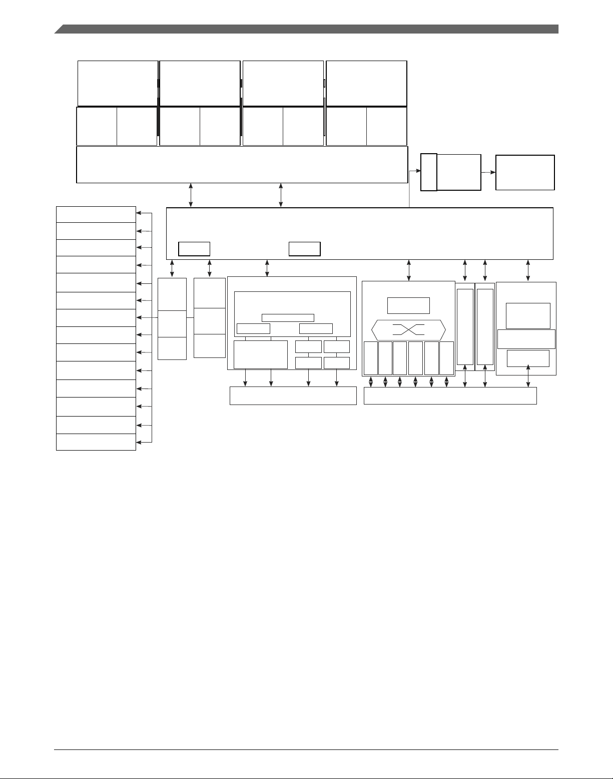
DMAx3
Power architecture
e6500
Power architecture
e6500
Power architecture
e6500
32 KB
D-Cache
2 MB Banked L2
Pre-Fetch
512 KB
Plat cache
64-bit DDR3/3L
with ECC
MPIC
Preboot loader
Security monitor
Internal bootROM
Power mgmt
SDXC/eMMC
eSPI
2 x DUART
4x I2C
2 x USB2.0 w/PHY
Clocks/reset
DCE
RMan
PME
BMan
SEC QMan
PAMU PAMU
CoreNet
coherency fabric
PAMU
(peripheral access management unit)
FMan
Parse, classify,
distribute
Buffer
HiGig
DCB
8 lanes up to 10 GHz SerDes
PCle
SATA2.0
Perf
Monitor
Watch point
crosstrigger
Aurora
Real-time
debug
32 KB
I-Cache
32 KB
D-Cache
32 KB
I-Cache
32 KB
D-Cache
32 KB
I-Cache
32 KB
D-Cache
32 KB
I-Cache
PCle
PCle
PCle
sRIO
SATA2.0
sRIO
8 lanes up to 8 GHz SerDes
CoreNet
trace
4x 1/2.5/1OG
1GE 1GE
1GE 1GE
GPIO
CCSR
IFC
Power architecture
e6500
Block diagram
Figure 1-1. T2080 block diagram
10 Freescale Semiconductor, Inc.
QorIQ T2080 Reference Design Board (T2080RDB-PC) User Guide, Rev. 0, 04/2016
Page 11
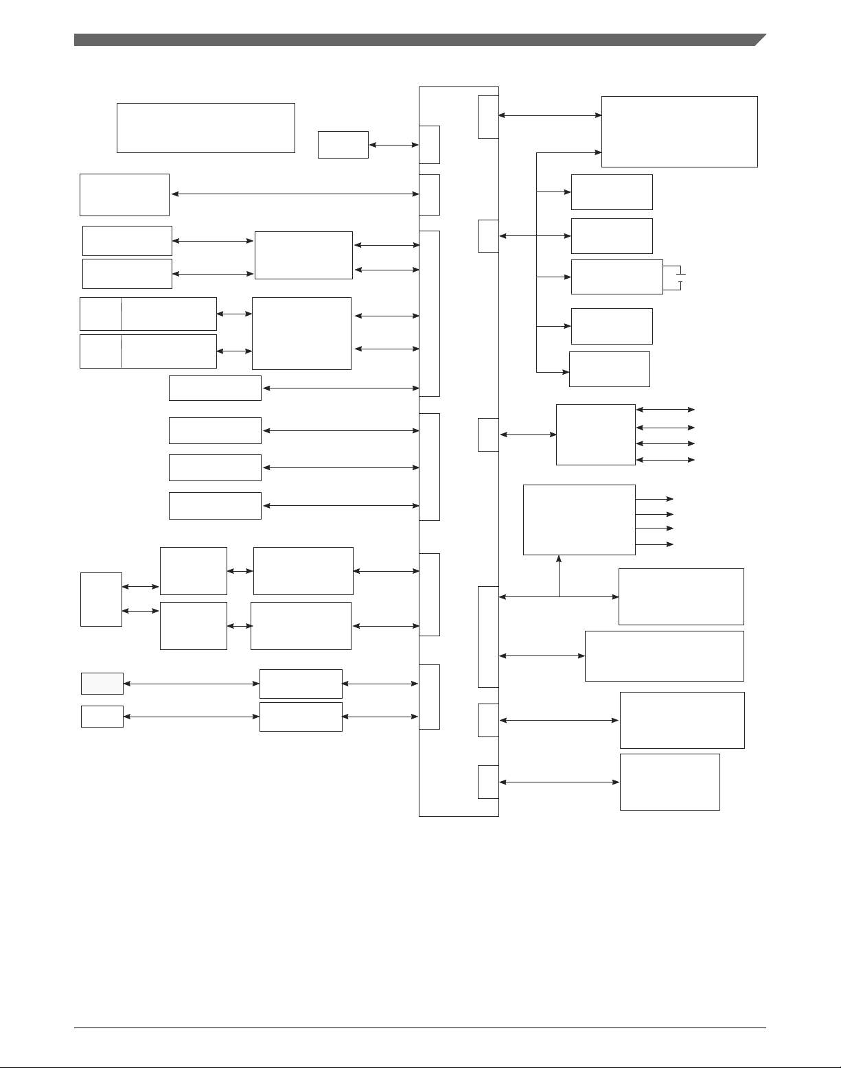
Clocks, POR, Reset, and
Power supply circuit
USB Conn *2
USB Type A x 2
SFI
SFI
XFI
XFI
CS4315
(XFI>SFI)
MDI
Transformer
RJ45
AQ1202
(XFI>10G BaseT)
PCle x4
PCle x4 slot
Golden finger
C293
coprocessor
SATA*2
SATA_conn
X2
Magnetic
(GSTS009LF)
RTL8211E-VB
(RGMII->Copper)
RGMII
RJ45
X2
Magnetic
(GSTS009LF)
RTL8211E-VB
(RGMII->Copper)
RGMII
MAX3232
TXD,RXD,RTS,CTS
TXD,RXD,RTS,CTS
RJ45
RJ45
Local Bus (16bit)
Local Bus (8bit)
SPI Bus
SDHC Bus
Micro SD card
SPI FLASH
N25Q512A13GSF40F
(64MB)
NAND FLASH
MT29F8G08ABABAWP-12IT
(1GB)
NOR FLASH
S29GL01GP11TFIV10
(128MB)
CPLD
(EPM570G)
PCA9546
Address:0x77
I2C2_PEX4S
NOT USE
I2C2_SFP2
I2C2_SFP1
RESET
Interrupt
Power-on conf
Other control
Address:0x08
Address:0x6A
Address:0x88
I2C_1
Address:0x40
Address:0x50
Battery Backup
RTC(DS1339U)
Temp Sensor
(ADT7481)
I2C EEPROM
(AT24C256)
Clock generator
(IDT9FGV0641)
Power regulator
(IR36021)
1.8 GHz, DDR3L/72bit 4GB
(SODIMM)
SPD Address:0x51
DDR3L 72bit
COP
USB2.0SerDes1
I2C_1
DDR3
I2C_2
SerDes 2
RGMII
IFC
DUART
SPI
SDHC
T2080
SFP+ 10G
Optics module
SFP+ 10G
Optics module
JTAG
XFI
XFI
MDI
Transformer
RJ45
PCle x4
PCle x2
MAX3232
Chapter 1 Overview
Figure 1-2. T2080RDB-PC architecture
QorIQ T2080 Reference Design Board (T2080RDB-PC) User Guide, Rev. 0, 04/2016
Freescale Semiconductor, Inc. 11
Page 12

Block diagram
QorIQ T2080 Reference Design Board (T2080RDB-PC) User Guide, Rev. 0, 04/2016
12 Freescale Semiconductor, Inc.
Page 13

Chapter 2
Architecture
This section explains the architecture of T2080RDB-PC:
• Processor
• Power
• Reset
• Clocks
• DDR
• SerDes port
• Ethernet controllers
• Ethernet Management Interface
• I2C
• SPI interface
• Local bus
• SDHC interface
• USB interface
• RS-232
• JTAG/COP port
• Connectors, Headers, Jumper, Push buttons, and LEDs
• Temperature
• DIP switch definition
2.1
The T2080RDB-PC supports many features of the T2080 processor, as detailed in the
following sections.
2.2
The power supply system of the T2080RDB-PC system uses power from a standard 6-pin
EPS, to provide power to the numerous processors, CPLD, and peripheral devices.
Freescale Semiconductor, Inc. 13
Processor
Power
QorIQ T2080 Reference Design Board (T2080RDB-PC) User Guide, Rev. 0, 04/2016
Page 14

Power
• Monolithic power supply for VCC (powering internal cores and platform logic)
• DUT-specific power rails are instrumented such that current measurement is possible
• Automatic collection of voltage, current, and power is performed for critical supplies
• Mounting holes are provided of sufficient size to allow onboard supplies to be
replaced by bench supplies
• All power supplies can be sequenced as per hardware specifications
The power supplies provided are organized into general categories and are described in
the individual sections.
The diagram below shows the power supply architecture.
QorIQ T2080 Reference Design Board (T2080RDB-PC) User Guide, Rev. 0, 04/2016
14 Freescale Semiconductor, Inc.
Page 15
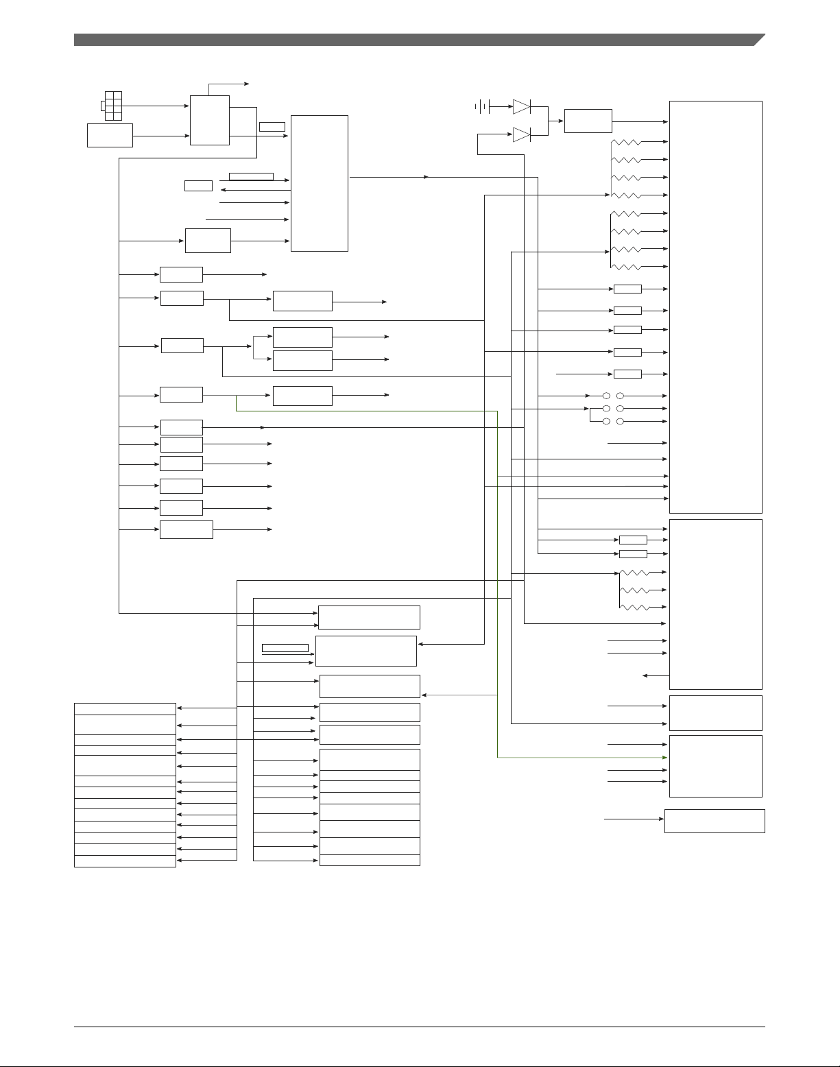
VDD_LP
AVDD_SD1_PLL1
AVDD_SD1_PLL2
AVDD_SD2_PLL1
AVDD_SD2_PLL2
0.33ohm
1V0_LP
NCP571
1V35
5.1ohm
AVDD_CGA1
AVDD_DDR1
AVDD_PLAT
AVDD_CGA1
USB_SVDD[1:2]
USB_HVDD[1:2]
USB_OVDD(1:2)
T2080
X1VDD[1:7]/X2VDD[1:6]
BEAT
VCORE
3V3
1V8
1V35
XVDD
S1VDD(1:6)/S2VDD[1:6]
SVDD
1V0S
FA_VL
PROG_MTR
PROG_SFP
D1_MVREF
MVREF
J10
J9
J11
1V8
VCORE
1V8
OVDD[1:11)/
TH_VDD/CVDD[1:2]
LVDD(1:3)/DVDD[1:2]
G1VDD[1:25]
VDD[1:60]
VCORE
1V35
2V5
1V8
AVDD_PLAT
VDD_CB
VDD_CA
VDDC/VDD_LL/VDD_LP
AVDD_CORE
AVDD_DDR
BVDD/O2VDD
3V3
1V0S2
1V5X
SVDD
XVDD
GND
CVDD/GVDD/LVDD/
OVDD/VDD/BVDD_VSEL
C293
1V0
1V8
1V2
V12/VA12
CS4315
V25_SRDS/V25_IO
LVDD
VDD
AQI1202
0V67
2V5
0V87
5V0
IN
USB: MIC2506(U24)
1V8
LDT9FGV0641
VCC
NAND FLASH(U68)
MT29F4G08ABBDAH4
74LVC373(U2)
SN74LVCIGS6(U7/9/11)
SN74LVC1GS6(U7/9/11)
Y66.66MHz(X3)
T2080 sys refclk
EPM570
NOR FLASH(U4)
828F00AM29EWHA
VCC
VCC
RTL8211E-VH(U35/U38)
VDD
3V3
ADT7481(U34)
AT24C256(U33)
DSI339U(U31)
MAX3232(U27)
MICX11(U67)
ICS843002(U47)
SFPX2(J13/J15)
OSC.32.768KHz(X2)
1.66.66MHz(X5)
C293 Sys_refclk
P13PCIE3212(U23)
Micro SD Card(12)
SPI FLASH(U13)
N25Q512A13G
PCA9516(U22)
12V
3V3
VTT/VREF
PCIEX4 SLOT(J20)
DDR3_SODIM_ECC
1V35
2V5
3V3 (5A)
5V0 (2A)
0V67 (4A)
0V78 (4A)
1V2(2A)
5V0H
For IR3473_VCC
MIC39102
IR3473
IR3475
12V
IR3473
IR3473
1VB (1.5A)
2V5 (2A)
1V35 (5A)
VTT/MVREF
1V0S
T2080_SVDD
1V0S2
C293_SVDD
1V5x
C290_XVDD
MIC47100
TPSS1200
IR3473
IR3475
1V0 (1A)
3V3
CPLD
VCC_DRV_3.3V
VCC_DRV_7V
MIC39102
YM
VPG
Regulator
IR36021/
3550
VCORE / 60A
Standalone_det
12VEPS
6PIN EPS
12V_PEX
Power
selection
12V
CPLD
3V3
BAT
VCORE
1V35
1V8
2V5
3V3
PM_BUS
VCORE_PGOOD
VCORE_EN
12V
12V
12V
12V
12V
12V
12V
12V
12V
12V
IR3473
IR3473
IR3473
MIC47100
MIC47100
0.33ohm
0.33ohm
0.33ohm
5.1ohm
5.1ohm
5.1ohm
1V8
BEAT
BEAT
BEAT
BEAT
VCORE
VCORE
VCORE
BEAT
BEAT
5.1ohm
5.1ohm
5.1ohm
VCC
VDD
VDD
VDD
VDD
VDD
VDD
VDD
VDD
VDD
VDD
3V3
3V3
3V3
3V3
3V3
3V3
3V3
3V3
3V3
3V3
3V3
3V3
1V8
1V8
1V8
1V8
1V8
1V8
1V8
1V8
1V8
3V3
3V3
3V3
3V3
VIO
VDD
VDD
VDD
VDD
VDD
VDD
VDD
Y133.33MHz(X4)
T2080 ddr refclk
Y24MHz(x1)
Usb_refclk
Golden
finger
VDD
Chapter 2 Architecture
Freescale Semiconductor, Inc. 15
Figure 2-1. Power supply
QorIQ T2080 Reference Design Board (T2080RDB-PC) User Guide, Rev. 0, 04/2016
Page 16

Golden finger
PEX4_RST_N
GND
Push-Button
MAX811S
(Power-on RST)
PWR_RST_N
COP_SRST_N
T2080
COP_ITF
T2080
HESET_REQ_N
HRSET_N
PORESET_N
C293
COP_ITF
C290_COP_HRST_N
C290_COP_SRST_N
C290_HESET_REQ_N
C290_HRSET_N
C293
C290 Reset
Logic
T2080
Reset
Source
select
RST_CTL
DDR_RSTN
NOR
FLASH
NOR_RSTN
PEX4S_RST
PEX SLOT
EDC_RST_N
CS4315
DVI_RST_N
10GBASET
PHY
AQ1202
EC1_RST_N
RGMII
GE PHY1
Soft reset register
RSTCON1 & RSTCON2
SW_RST
7
CPLD
COP_HRST_N
6
5
4
3
2
1
0
EC2_RST_N
RGMII
GE PHY2
DDR3/
DDR3L
Clocks
2.3 Reset
Reset signals to and from the T2080 processor and other devices on the T2080RDB-PC
are managed by CPLD. The diagram below shows an overview of the reset architecture.
2.4
The clock circuitry provides clocks for the processor, for:
Clocks
Figure 2-2. Reset architecture
• SYSCLK
• DDRCLK (single-ended and differential)
• SerDes clocks
• Ethernet clocks
• USB clock
QorIQ T2080 Reference Design Board (T2080RDB-PC) User Guide, Rev. 0, 04/2016
16 Freescale Semiconductor, Inc.
Page 17

The architecture of the clock section is shown in the diagram below.
OSC-66.66MHz
OSC-133.33MHz
OSC-24MHz
25MHz
ICS843002
Golden finger
EDC_REFCLK_P/N(156.25MHz)
SD1_REFCLK1_P/N(156.25MHz)
PEX4_REFCLK_P/N(100MHz)
PI3PCIE3212
CS4315
USB_REFCLK(24MHz)
DDRCLK(133.33MHz)
SYSCLK(66.66MHz)
T2080
SD1_REFCLK1_P/N
SD1_REFCLK2_P/N
SD2_REFCLK1_P/N
SD2_REFCLK2_P/N
PEX
SLO
T
C293
SD1_REFCLK2_P/N(100MHz)
PEX_CLK_P/N(100MHz)
IDT9FGV0641
SD2_REFCLK1_P/N(100MHz)
C290_SYSCLK (66.66MHz)
OSC-66.66MHz
SD2_REFCLK2_P/N(100M)
PEX4S_REFCLK_P/N(100M)
C290_SD_REFCLK_P/N(100M)
25MHz
Chapter 2 Architecture
Figure 2-3. Clock architecture
QorIQ T2080 Reference Design Board (T2080RDB-PC) User Guide, Rev. 0, 04/2016
Freescale Semiconductor, Inc. 17
Page 18

IV35
187Ohm
187Ohm
DDR_DQ[0:63]
DDR_ECC[0:7]
DDR_MA[0:15]
DDR_MDQS[0:8]
DDR_MDM[0:8]
DDR_MBA[0:2]
DDR_MDOT[0:1],DDR_MAPAR_OUT,DDR_MPAR_ERR
DDR_MCS[0:3]
DDR_MCK_P[0:1]_P/N
DDR_CAS,DDR_RAS,DDR_WE
DDR_MCKE[0:1]
IV35
DDR_RST_N
(CPLD)
I2C1_SCL,I2C1_SDA
MV_REF
VTT
IV35
(SPD_ADDR=0X51)
DDR3 SODIMM SOCKET
DIMM
T2080
DI_MDICI
DI_MDICO
IR3475
TPS
51200
SerDes port
2.5 DDR
The T2080RDB-PC supports high-speed DRAM, with an SODIM socket, featuring
single, dual, and quad-rank support. The memory interface includes the necessary
termination and I/O power and is routed so as to achieve maximum performance of the
memory bus, as shown in the diagram below.
Figure 2-4. Memory interface
2.6
The T2080 SerDes block provides 16 high-speed serial communication lanes, supporting
SerDes port
a variety of protocols, including:
QorIQ T2080 Reference Design Board (T2080RDB-PC) User Guide, Rev. 0, 04/2016
18 Freescale Semiconductor, Inc.
Page 19

Chapter 2 Architecture
• SGMII 1.25 / 3.125 Gbit/s
• PCI Express (PEX) Gen 1 1X / 2X / 4X 2.5 Gbit/s
• PCI Express (PEX) Gen 2 1X / 2X / 4X 5 Gbit/s
• SATA 1X 1.5 / 3 Gbit/s
The T2080 additionally supports these protocols:
• PCI Express (PEX) Gen 3 1X 8 Gbit/s
• XFI 1X 10.3125 Gbit/s
An overview of the SerDes protocols, which are supported on the T2080RDB, is shown
in the table below.
Table 2-1. SerDes protocols
SERDES1
SRDS_PRTCL_S1 A B C D E F G H Per lane PLL mapping
66 XFI9 XFI10 XFI1 XFI2 PCIe4 1111
2222
SERDES2
SRDS_PRTCL_S2 A B C D E F G H Per lane PLL mapping
15 PCIe1 PCIe2PCIe2SATA1SATA21111
1122
The image below shows the SerDes distribution of T2080RDB-PC.
QorIQ T2080 Reference Design Board (T2080RDB-PC) User Guide, Rev. 0, 04/2016
Freescale Semiconductor, Inc. 19
Page 20

10G
10G
1G
1G
10G
10G
10GBaseT
XFI.
9-
10G
RGMII
RGMII
SERDES 1 66
XFI.1-
10G XFI.2-10G
T2080
SERDES 2 15
PCle2
SATA
FSL
C293
SATA
Conn
PCle x 4 Gen3 support
XFI.
10-
10G
PCle
SATA
SATA
Conn
10GBaseT
PCle1 x 4
Gen2
PCle4 x 4
Gen3
X4 PCle
Gen3 slot
SerDes port
Figure 2-5. SerDes distribution of T2080RDB-PC
2.6.1
PCI Express support
The T2080RDB-PC supports PCIe x4 Gen 3 for golden finger and PCIe x4 Gen 2 for
slot.
2.6.2
XFI 10G optics port support
The T2080 supports evaluation of the XFI protocol using Cortina CS4315 dual port 10G
CDR. 10G data is carried over the XFI interface. The image below shows the
connectivity of XFI interface.
QorIQ T2080 Reference Design Board (T2080RDB-PC) User Guide, Rev. 0, 04/2016
20 Freescale Semiconductor, Inc.
Page 21

T2080
XFI
XFI
EMI2
XFI
XFI
EMI2
CS4315
Dual 10G EDC
SFP+
SFP+
SFI
SFI
Figure 2-6. XFI interface
T2080
XFI
XFI
EMI2
XFI
XFI
EMI2
AQI202
Dual 10G Base - T PHY
MDI
Magnetics
RJ46
MDI
Magnetics
RJ46
Chapter 2 Architecture
2.6.3
XFI 10GBase-T port support
The T2080 only supports evaluation of the XFI protocol using Aquantia AQ1202 dual
port 10GBase-T PHY. 10G data is carried over the XFI interface. The image below
shows the connectivity of XFI interface.
Figure 2-7. XFI interface
2.6.4
SATA support
SATA is evaluated using the two onboard SATA headers, by selecting a SATAsupporting SerDes protocol.
2.7
Ethernet controllers
The T2080 supports two Ethernet Controllers (EC), which can connect to Ethernet PHYs
using MII or RGMII protocols. On the T2080RDB-PC, the EC1 and EC2 ports only
operates in RGMII mode. Both ports connect to Realtek RTL8211 PHYs.
The image below shows the connectivity of EC1/EC2 interface.
Freescale Semiconductor, Inc. 21
QorIQ T2080 Reference Design Board (T2080RDB-PC) User Guide, Rev. 0, 04/2016
Page 22

RGMII
MDIO/MDC
ETH. Cntr. 1
T2080
EMII
RGMII
RGMII
MDIO/MDC
RTL8211E_VB
Transformer
Transformer
RJ-45 Port
RJ-45 Port
ETH. Cntr. 2
EMII
RGMII
RTL8211E_VB
Ethernet Management Interface
Figure 2-8. EC1/EC2 interface connectivity
2.8
Ethernet Management Interface
The T2080 has two Ethernet Management Interfaces (EMI), both powered by LVDD.
However, EMI2 is only used with XFI based PHYs, which uses 1.2 V pull-up. EMI1 is
used with all other non-XFI based PHYs, including the onboard RGMII PHYs. The
image below shows the EMI hardware block.
22 Freescale Semiconductor, Inc.
QorIQ T2080 Reference Design Board (T2080RDB-PC) User Guide, Rev. 0, 04/2016
Page 23

1V2
2V5
EMI1_MDC
EMI1_MDIO
RTL8211E-VB
(RGMII PHY)
RTL8211E-VB
(RGMII PHY)
CS4315
10G CDR
AQ1202
10G-BASET
PHY_ADDR=0x01
PHY_ADDR=0X02
PHY1_ADDR=0X0C
PHY2_ADDR=0X0D
PHY1_ADDR=0X00
PHY2_ADDR=0X01
EMI1_MDC
EMI1_MDIO
T2080
EMI2_MDC
EMI2_MDIO
Chapter 2 Architecture
Figure 2-9. EMI hardware block
2.9
I2C
The T2080 devices supports up to four I2C buses, in order to make the I2C resources
equally available to both local and remote systems. The T2080RDB-PC uses I2C1 port to
access onboard devices, such as DDR3 DIMM, RTC, I2C EEPROM, clock generator,
thermal sensor (ADT7481), and core power regulator (IR36021). The I2C2 bus uses
multiplexers to partition the I2C bus into several sub-buses, called channels. Two SFP+
optics use channel 0-1 and the PCIe SLOT use channel 3.
The image below shows the I2C subsystem.
QorIQ T2080 Reference Design Board (T2080RDB-PC) User Guide, Rev. 0, 04/2016
Freescale Semiconductor, Inc. 23
Page 24

FET Isolation
(TRLML6346)
I2C1
I2C1_SCL
3V3
2V5
DDR3 DIMM
ADT7481
(Thermal Sensor)
AT24C256
DSI339U
IDT9FGV0641
IR36021
I2C_ADDR=0x51
SFP+ optics
NOT USE
SFP+ optics
PCle SLOT
I2C2_SFP1SCL
I2C2_SDA
I2C2_SCL
I2C2
Channel 3
Channel 2
PCA9546
Channel 1
Channel 0
I2C_ADDR-0X77
T2080
I2C1_SDA
I2C2_SFP1_SDA
I2C2_SFP2_SCL
I2C2_SFP2_SDA
I2C2_CHAN2_SCL
I2C2_CHAN2_SDA
I2C2_PEX4S_SCL
I2C2_PEX4S_SDA
I2C_ADDR=0x4C
I2C_ADDR=0x50
I2C_ADDR=0x68
I2C_ADDR=0x6A
I2C_ADDR=0x08
I2C_ADDR=
0x50
I2C_ADDR=
0x50
2V5
SPI interface
Figure 2-10. I2C subsystem
QorIQ T2080 Reference Design Board (T2080RDB-PC) User Guide, Rev. 0, 04/2016
24 Freescale Semiconductor, Inc.
Page 25

T2080
ADDR,DATA,Control
TXBN0304
(1.8V->3.3V)
CPLD
Cfg_vbank[0:2]
IFC_A5-A7
XORs
IFC_VA5-7
NOR_CS
NOR FLASH
(JS28F00AM29EWHA)
NAND_CS
NAND FLASH
(MT29F8G08ABABA WP)
(3.3V)
Chapter 2 Architecture
2.10 SPI interface
The T2080RDB-PC Serial Peripheral Interface (SPI) pins is only used for onboard SPI
device accessing various SPI memory devices.
2.11 Local bus
The T2080 Integrated Flash Controller (IFC), also known as the local bus, supports 32-bit
addressing and 8 or 16-bit data widths for a variety of devices to effectively manage all
these resources with the maximum amount of performance and flexibility.
The image below shows an overview of the IFC bus.
2.12
SDHC interface
Figure 2-11. IFC bus
The enhanced SD Host Controller (eSDHC) provides an interface between host system
and SD cards. The Secure Digital (SD) card is specifically designed to meet the security,
capacity, performance, and environmental requirements, inherent in emerging audio and
video consumer electronic devices. Booting from eSDHC interface is supported using the
processor’s on-chip ROM.
QorIQ T2080 Reference Design Board (T2080RDB-PC) User Guide, Rev. 0, 04/2016
Freescale Semiconductor, Inc. 25
Page 26

T2080
SD_WP
SD_CD
SDHC_CLK
CMD
DAT[0:3]
TXBN0304
Clamping
diodes
3V33V3
WP
CD
CLK
CMD
DAT[0:3]
Micro
SD Card
USB interface
On T2080RDB-PC, a single connector is used for MicroSD memory cards, as shown in
the image below.
Figure 2-12. SDHC interface
2.13
USB interface
The T2080RDB-PC systems have two integrated USB 2.0 controllers, that allow direct
connection to USB ports with appropriate protection circuitry and power supplies.
The board features are:
• High speed (480 Mbit/s), full-speed (12 Mbit/s), and low-speed (1.5 Mbit/s)
operation
• Host mode
• Dual stacked Type A connection
The USB ports connect to a standard Type A connector (USB1 and USB2) for
compatibility with most USB peripherals.
Power for the ports is provided by a MIC2506YM, which supplies 5 V at up to 1 A per
port. The power enable and power-fault-detect pins are connected directly to the T2080
for individual port management.
The image below shows how the USB connectivity is implemented on the T2080RDBPC.
QorIQ T2080 Reference Design Board (T2080RDB-PC) User Guide, Rev. 0, 04/2016
26 Freescale Semiconductor, Inc.
Page 27

T2080
USB1_UID
USB1_UDP, UDM
USB1_VBUSCLMP
USB1USB2
USB2_VBUSCLMP
USB2_DRVVBUS
USB2_PWRFAULT
USB1_DRVVBUS
USB1_PWRFAULT
USB2_UDP, UDM
USB2_UID
IBIAS_REXT
INSTALLED: Host mode (default)
90 OHm diff.imp.
CMHD3595
USB Type A
CMHD3595
10K
1%
24MHz
USB CLK
USB CLKIN
90 OHm diff.imp.
USB Type A
INSTALLED: Host mode (default)
5Vz
18.2K
51.1K
18.2K 51.1K
MIC2506YM
Chapter 2 Architecture
Figure 2-13. USB connectivity implementation
2.14
The T2080 processor has two UART controllers, which provides an RS-232 standard
RS-232
interconnection between the board and an external host. The serial connection is typically
configured to run at 11.5 Kbit/s.
QorIQ T2080 Reference Design Board (T2080RDB-PC) User Guide, Rev. 0, 04/2016
Freescale Semiconductor, Inc. 27
Page 28

RS232_TXD1
RS232_RXD1
RS232_TXD2
RS232_RXD2
PROC_UART2_RXD
PROC_UART2_TXD
PROC_UART1_RXD
PROC_UART1_TXD UART1_TXD
UART1_RXD
UART2_TXD
UART2_RXD
3V3
3V32V5
2V5 3V3
C96 0.1uF
C105
0.1uF
C94 0.1uF
C97 0.1uF
C106
0.1uF
FB8
BLM18BD601SN1
R177 100
R176 100
C100
470pF
DUART ( DVDD)
U1J
T2080
UART1_SOUT
J1
UART1_SIN
J3
UART1_RTS_B
G1
UART1_CTS_B
L4
UART2_SOUT
K3
UART2_SIN
F2
UART2_RTS_B
J4
UART2_CTS_B
F1
C102
470pF
C98 0.1uF
R175 100
RS-232 XCVR
U27
MAX3232
C1+
1
C1-
3
C2+
4
C2-
5
GND
15
R1-IN
13
R1-OUT
12
R2-IN
8
R2-OUT
9
T1-IN
11
T1-OUT
14
T2-IN
10
T2-OUT
7
V+
2
V-
6
VCC
16
FB6
BLM18BD601SN1
R640
4.7K
FB9
BLM18BD601SN1
C101
470pF
R641
4.7K
R174 100
C95 0.1uF
U28
TXBN0304RSV
A1
1
A2
2
A3
3
A4
4
NC1
5
GND
6
GND
7
OE
8
B4
9
B3
10
B2
11
B1
12
VCCB
13
VCCA
16
NC2
14
NC3
15
C99
470pF
FB7
BLM18BD601SN1
JTAG/COP port
Each UART supports:
• Full-duplex operation
• Software-programmable baud generators
• Software-selectable serial interface data format, that includes:
• Data length
• Parity
• 1/1.5/2 STOP bit
• Baud rate
• Overrun, parity, and framing error detection
The UART ports are routed to 3PIN connectors, as shown in the image below.
Figure 2-14. UART ports, routed to 3PIN connectors
The table below shows the connection setting for the UART 3pin connector to DB9
female cable connection.
Table 2-2. PIN3 to DB9 connection setting
3PIN connector RS-232 signal DB9 female pin number
1 TXD 2
2 GND 5
3 RXD 3
Before powering up the T2080RDB card, configure the serial port of the attached
computer with the following values:
• Data rate: 115200 bit/s
• Number of data bits: 8
• Parity: None
• Number of stop bits: 1
• Flow control: Hardware/None
QorIQ T2080 Reference Design Board (T2080RDB-PC) User Guide, Rev. 0, 04/2016
28 Freescale Semiconductor, Inc.
Page 29

TDO
TDI
NC
TCK
TMS
SRESET_B
HRESET_B
CKSTP_OUT
GND
NC
GND
NC
CKSTP_IN
VDD_SENSE
TRST_B
NC
1
Chapter 2 Architecture
2.15 JTAG/COP port
The common on-chip processor (COP) is a part of the T2080’s JTAG module and is
implemented as a set of additional instructions and logic. This port can connect to a
dedicated emulator for extensive system debugging. Several third-party emulators in the
market can connect to the host computer through the Ethernet port, USB port, parallel
port, or RS-232. A typical setup using a USB port emulator is shown in the image below.
Figure 2-15. USB port emulator setup
The 16-pin generic header connector carries the COP/JTAG signals and the additional
signals for system debugging. The pin-out of this connector is shown in the image below.
Figure 2-16. 16-pin connector
QorIQ T2080 Reference Design Board (T2080RDB-PC) User Guide, Rev. 0, 04/2016
Freescale Semiconductor, Inc. 29
Page 30

Connectors, Headers, Jumper, Push buttons, and LEDs
The table below displays the connections made from the T2080RDB-PC COP connector.
Table 2-3. Connections made from the T2080RDB-PC COP connector
Pin no. Signal name Connection
1 TDO Connected directly between the processor and JTAG/COP connector.
2 NC Not connected.
3 TDI Connected directly between the processor and JTAG/COP connector.
4 TRST Routed to the RESET PLD. TRST to the processor is generated from the PLD.
5 NC Not connected.
6 VDD_SENSE Pulled to 3.3 V using a 10 Ohm resistor.
7 TCK Connected directly between the processor and JTAG/COP connector.
8 CKSTP_IN Connected directly between the processor and JTAG/COP connector.
9 TMS Connected directly between the processor and JTAG/COP connector.
10 NC Not connected.
11 SRESET Routed to the RESET PLD. SRESET to the processor is generated from the PLD.
12 GND Connected to guard.
13 HRESET Routed to the RESET PLD. HRESET to the processor is generated from the PLD.
14 KEY Not connected.
15 CKSTP_OUT Connected directly between the processor and JTAG/COP connector.
16 GND Connected to guard.
2.16 Connectors, Headers, Jumper, Push buttons, and LEDs
This section explains:
• Connectors
• Headers
• Jumper
• Push buttons
• LEDs
2.16.1
Table 2-4 lists the various connectors on the T2080RDB-PC platform.
Reference designators Used for Notes
J28 6-pin EPS connector J2 MicroSD card -
Connectors
Table 2-4. Connectors on the T2080RDB-PC platform
Table continues on the next page...
QorIQ T2080 Reference Design Board (T2080RDB-PC) User Guide, Rev. 0, 04/2016
30 Freescale Semiconductor, Inc.
Page 31

Chapter 2 Architecture
Table 2-4. Connectors on the T2080RDB-PC platform (continued)
Reference designators Used for Notes
J20 PCIe x4 slot Intended use is for PCIe cards that are 25 W or less.
J21, J22 SATA J43 TDM Riser card J36, J37 Ethernet ports RGMII -> Copper
J17, J18 Ethernet ports 10GBase-T
J13, J15 Ethernet ports 10G optics
J41 Dual Type A USB J35 (2 ports) UART J8 Battery holder J1 SODIM J22, J23 FXS ports J24 FXO port J34 CPU fan J33, J44-J46 Shelf FAN -
2.16.2 Headers
The table below lists the various headers on the T2080RDB-PC platform.
Table 2-5. Headers on the T2080RDB-PC platform
Reference designators Used for Notes
J24 Altera Header Used for programming the Altera CPLD devices.
J26 IR36021 Header Used for programming the IR36021.
J3 COP/JTAG Used for debugging the T2080.
2.16.3 Jumper
The table below describes how the push Jumper is used on the T2080RDB-PC platform.
Table 2-6. Jumper on the T2080RDB-PC platform
Reference
designator
J29 Battery selection for VDD_LP
source
J30 Tamper detection pin powered
selection
Description Status 1 Status 2
Mounted: Battery acts as a
VDD_LP input source
1-2: Tamper detection pin is
powered on
Unmounted: Battery is
disconnected
2-3: Tamper detection pin is
powered off
Table continues on the next page...
QorIQ T2080 Reference Design Board (T2080RDB-PC) User Guide, Rev. 0, 04/2016
Freescale Semiconductor, Inc. 31
Page 32

Temperature
Table 2-6. Jumper on the T2080RDB-PC platform (continued)
Reference
designator
J9 PROG_SFP selection Mounted: Fuse programming Unmounted: Normally operate
J25 Not used - J38 SD/TF card voltage selection 1-2: TF card works at 3.3 V 2-3: TF card works at 1.8 V
Description Status 1 Status 2
2.16.4 Push buttons
The table below describes what the push buttons are used for on the T2080RDB-PC
platform.
Table 2-7. Push buttons on T2080RDB-PC platform
Reference designators Used for Notes
SW5 Reset Used for resetting the whole board.
SW4 Power on/off Used for turning the power on or off.
2.16.5 LEDs
Table 2-8 lists all the LEDs on the T2080RDB-PC front plate.
Table 2-8. LEDs on the T2080RDB-PC front plate
LEDs Used for Controlled by
D12 Power on +3.3V rail
D4 SFP1_LED0 CPLD
D5 SFP1_LED1 CPLD
D6 SFP2_LED0 CPLD
D7 SFP2_LED1 CPLD
QorIQ T2080 Reference Design Board (T2080RDB-PC) User Guide, Rev. 0, 04/2016
32 Freescale Semiconductor, Inc.
Page 33

I2C Bus
T2080
TEMP_ANODE
Thermal sensor
ADT7481
DXP1
DXN1
TEMP_CATHODE
DXP2
DXN2
THERM
ALERT/THERM2
OVER ALARM
THERM ALARM
CPLD
PWM
FAN_Power
TEMP_CATHODE
TEMP_ANODE
C29x
Chapter 2 Architecture
2.17 Temperature
The T2080 has a thermal diode attached to the die, allowing direct temperature
measurement. These pins are connected to an ADT7481 3 channel thermal monitor. One
channel monitors the T2080 and another channel monitors the C29x, which allows direct
reading of the temperature of the die and is accurate to ±1 °C. The third channel of the
ADT7481 measures the ambient (board) temperature.
The ADT7481 temperature warning and alarm signals are connected to the CPLD for
monitoring. CPLD uses these signals to adjust CPU FAN speed and protect the CPU
from over-temperature failure.
Figure 2-17. Temperature
QorIQ T2080 Reference Design Board (T2080RDB-PC) User Guide, Rev. 0, 04/2016
Freescale Semiconductor, Inc. 33
Page 34

T2080
POR & Override
CPLD Register
CPLD
cfg_xxx
switch
DIP switch definition
2.18 DIP switch definition
The T2080RDB-PC board has user selectable switches, for evaluating different boot
configurations and other special configurations for this device.
This configuration allows either the switch or the CPLD register to set the POR pin. The
CPLD register allows software to override the pin remotely when the board is in the
board farm.
In order to use the CPLD override option, software sets an override bit, that allows the
CPLD to override the switch setting during power on reset.
Figure 2-18. DIP switch definition
Table 2-9 shows how POR configuration is done through switches.
Table 2-9. POR configuration through switches
Switch Signal name Pin name Signal meaning Setting
SW1[1:8] cfg_rcw_src[0:7] IFC_AD[8:15] Reset Configuration word source.
For details, see T2080 Integrated
Multicore Communications
SW2[1] cfg_rcw_src[8] IFC_CLE Reset Configuration word source For details, see T2080
SW2[2] cfg_ifc_te IFC_TE IFC external transceiver enable
QorIQ T2080 Reference Design Board (T2080RDB-PC) User Guide, Rev. 0, 04/2016
34 Freescale Semiconductor, Inc.
Table continues on the next page...
Processor Family Reference
Manual (document T2080RM)
polarity select
NOR boot: 00010011_1
NAND boot: 10000010_1
SPI boot: 00100010_1
SD boot: 00100000_0
Integrated Multicore
Communications Processor
Family Reference Manual
(document T2080RM)
0: IFC drives logic 1 for TE
assertion
Page 35

Chapter 2 Architecture
Table 2-9. POR configuration through switches
(continued)
Switch Signal name Pin name Signal meaning Setting
1: IFC drives logic 0 for TE
assertion
SW2[3] cfg_pll_config_sel_bIFC_A18 Reserved Reserved
SW2[4] cfg_por_ainit IFC_A19 Reserved Reserved
SW2[5:6] cfg_svr[0:1] IFC_A[16:17] Reserved Reserved
SW2[7] cfg_dram_type IFC_A21 DRAM type selection 1: DDR3L(1.35V)
SW2[8] cfg_rsp_dis IFC_AVD Reserved Reserved
SW3[1] cfg_eng_use0 IFC_WE0 Sys_clock selection 1: Single sys_clk is selected
SW3[2:3] cfg_eng_use[1:2] Reserved Reserved SW3[4] BOOT_FLASH_SEL- Boot flash selection SW3[4] = 0 for NOR boot
SW3[4] = 1 for NAND boot
See note
SW3[5:7] CFG_VBANK[0:2] - NOR flash bank select 000: bank0
100: bank4
See note
SW3[8] TEST_SEL_N TEST_SEL_B - 1:T2080
1
2
1. For SW3[4]: BOOT_FLASH_SEL, it can act as boot flash selection, when BOOT_FLASH_SEL=1, NOR flash is boot flash
or NAND flash is boot flash.
2. SW3[5:7] can be used to change the staring address for the memory banks. The NOR flash memory is divided into eight
memory banks with 16 MB size each. Eight different U-Boot image can be programmed into each memory bank. When
NOR flash is selected as boot flash (CS0 is connected to NOR flash by setting SW3[4] to ON, RCW[0:8] is set to
0_0111_xxxx using SW1[1:8] and SW2[1]), different U-Boot image can be selected to boot up the board, by setting
SW3[5:7].
QorIQ T2080 Reference Design Board (T2080RDB-PC) User Guide, Rev. 0, 04/2016
Freescale Semiconductor, Inc. 35
Page 36

DIP switch definition
QorIQ T2080 Reference Design Board (T2080RDB-PC) User Guide, Rev. 0, 04/2016
36 Freescale Semiconductor, Inc.
Page 37

Chapter 3
CPLD Specification
This section explains the CPLD registers.
3.1 CPLD Memory Map
memory map
Offset
address
(hex)
0 Chip ID1 register (CHIPID1) 8 R 55h 3.1.1/37
1 Chip ID2 register (CHIPID2) 8 R AAh 3.1.2/38
2 Hardware version register (HWVER) 8 R See section 3.1.3/38
3 Software version register (SWVER) 8 R See section 3.1.4/39
10 Reset control register (RSTCON) 8 w1c See section 3.1.5/39
11 Flash control and status register (FLHCSR) 8 R/W See section 3.1.6/40
12 Thermal control and status register (THMCSR) 8 R/W See section 3.1.7/40
13 Panel LED control and status register (LEDCSR) 8 R/W See section 3.1.8/41
14 SFP+ control and status register (SFPCSR) 8 R/W See section 3.1.9/41
15 Miscellanies control and status register (MISCCSR) 8 R/W See section 3.1.10/42
16 Boot configuration override register (BOOTOR) 8 R/W See section 3.1.11/43
17 Boot configuration register 1 (BOOTCFG1) 8 R/W See section 3.1.12/43
18 Boot configuration register 2 (BOOTCFG2) 8 R/W See section 3.1.13/43
Register name
Width
(in bits)
Access Reset value
3.1.1 Chip ID1 register (CHIPID1 )
Section/
page
Address: 0h base + 0h offset = 0h
Bit 0 1 2 3 4 5 6 7
Read CHIPID1
Write
Reset
Freescale Semiconductor, Inc. 37
0 1 0 1 0 1 0 1
QorIQ T2080 Reference Design Board (T2080RDB-PC) User Guide, Rev. 0, 04/2016
Page 38

CPLD Memory Map
CHIPID1 field descriptions
Field Description
0–7
CHIPID1
0x55, Identification of the CPLD image.
3.1.2 Chip ID2 register (CHIPID2)
Address: 0h base + 1h offset = 1h
Bit 0 1 2 3 4 5 6 7
Read CHIPID2
Write
Reset
Field Description
0–7
CHIPID2
1 0 1 0 1 0 1 0
CHIPID2 field descriptions
0xaa, Identification of the CPLD image.
3.1.3 Hardware version register (HWVER)
Hardware version register.
Address:
0h base + 2h offset = 2h
Bit 0 1 2 3 4 5 6 7
Read HW_VER
Write
Reset
0 0 0 0 0 0 0 0
HWVER field descriptions
Field Description
0–7
HW_VER
The version field of the hardware board.
QorIQ T2080 Reference Design Board (T2080RDB-PC) User Guide, Rev. 0, 04/2016
38 Freescale Semiconductor, Inc.
Page 39

3.1.4 Software version register (SWVER)
Address: 0h base + 3h offset = 3h
Bit 0 1 2 3 4 5 6 7
Read SW_VER
Write
Reset
0 0 0 0 0 0 0 0
SWVER field descriptions
Field Description
0–7
SW_VER
The version field of the CPLD software.
3.1.5 Reset control register (RSTCON)
Chapter 3 CPLD Specification
Address: 0h base + 10h offset = 10h
Bit 0 1 2 3 4 5 6 7
Read SW_RST C293_RST
Write w1c
Reset
0 0 0 0 0 0 0 0
w1c
Reserved
EC1_RST EC2_RST EDC_RST XGT_RST PEX_RST
w1c w1c w1c w1c w1c
RSTCON field descriptions
Field Description
0
SW_RST
1
C293_RST
2
-
3
EC1_RST
4
EC2_RST
5
EDC_RST
6
XGT_RST
7
PEX_RST
0: No reset occurs.
1: Writing logic 1 will produce whole board reset# signal; this bit can auto clear.
0: No reset occurs.
1: Writing logic 1 will produce C293 Coprocessor reset# signal; this bit can auto clear.
This field is reserved.
0: No reset occurs.
1: Writing logic 1 will produce RGMII PHY1 (RTL82111E-VB) reset# signal; this bit can auto clear.
0: No reset occurs.
1: Writing logic 1 will produce RGMII PHY2 (RTL82111E-VB) reset# signal; this bit can auto clear.
0: No reset occurs.
1: Writing logic 1 will produce 10GEDC PHY(CS4315) reset# signal; this bit can auto clear.
0: No reset occurs.
1: Writing logic 1 will produce 10GBase-T PHY(AQ1202) reset# signal; this bit can auto clear.
0: No reset occurs
1: Writing logic 1 will produce PCIe x4 slot reset# signal; this bit can auto clear.
QorIQ T2080 Reference Design Board (T2080RDB-PC) User Guide, Rev. 0, 04/2016
Freescale Semiconductor, Inc. 39
Page 40

CPLD Memory Map
3.1.6 Flash control and status register (FLHCSR)
Address: 0h base + 11h offset = 11h
Bit 0 1 2 3 4 5 6 7
Read BOOT_SEL
Write
Reset
n 0 n n n 0 0 0
BANK_OR
SW_BANK_
SEL0
FLHCSR field descriptions
Field Description
0
BOOT_SEL
1
BANK_OR
2
SW_BANK_SEL0
3
SW_BANK_SEL1
4
SW_BANK_SEL2
5
BANK_SEL0
6
BANK_SEL1
7
BANK_SEL2
0: Boot from 16-bit NOR flash.
1: Boot from 8-bit NAND flash.
0: NOR flash bank select from CPLD override disable.
1: NOR flash bank select from CPLD override enable.
0: NOR flash bank select bit0 of switch status is 0.
1: NOR flash bank select bit0 of switch status is 1.
0: NOR flash bank select bit1 of switch status is 0.
1: NOR flash bank select bit1 of switch status is 1.
0: NOR flash bank select bit2 of switch status is 0.
1: NOR flash bank select bit2 of switch status is 1.
0: NOR flash bank select bit0 set 0.
1: NOR flash bank select bit0 set 1.
0: NOR flash bank select bit1 set 0.
1: NOR flash bank select bit1 set 1
0: NOR flash bank select bit2 set 0.
1: NOR flash bank select bit2 set 1.
SW_BANK_
SEL1
SW_BANK_
SEL2
BANK_
SEL0
BANK_
SEL1
BANK_
SEL2
3.1.7 Thermal control and status register (THMCSR)
Address: 0h base + 12h offset = 12h
Bit 0 1 2 3 4 5 6 7
Read
Write
Reset
THM_
FAULT
n n 0 0 1 1 1 1
QorIQ T2080 Reference Design Board (T2080RDB-PC) User Guide, Rev. 0, 04/2016
40 Freescale Semiconductor, Inc.
THM_
ALERT
Reserved FAN_PWM
Page 41

Chapter 3 CPLD Specification
THMCSR field descriptions
Field Description
0
THM_FAULT
1
THM_ALERT
2–3
-
4–7
FAN_PWM
0: Thermal sensor no fault occurs.
1: Thermal sensor fault output.
0: Thermal sensor no alert occurs.
1: Thermal sensor alert output.
This field is reserved.
0000: PWM duty cycle is 0%, fan stop running.
0001 - 1110: PWM duty cycle is 6.7% - 93.3%, fan speed control.
1111: PWM duty cycle is 100%, fan full speed.
3.1.8 Panel LED control and status register (LEDCSR )
Address: 0h base + 13h offset = 13h
Bit 0 1 2 3 4 5 6 7
Read
Write
Reset
STS_LED Reserved
0 0 0 0 0 0 0 0
LEDCSR field descriptions
Field Description
0
STS_LED
1–7
-
0: Panel STATUS LED on.
1: Panel STATUS LED flash at 0.5s.
This field is reserved.
3.1.9 SFP+ control and status register (SFPCSR )
Address: 0h base + 14h offset = 14h
Bit 0 1 2 3 4 5 6 7
Read SFP1_DET
Write
Reset
n 0 n n n 0 n n
SFP1_
TXDIS
SFP1_
RXLOS
SFP1_
TXFAIL
SFP2_DET
SFP2_
TXDIS
SFP2_
RXLOS
SFP2_
TXFAIL
QorIQ T2080 Reference Design Board (T2080RDB-PC) User Guide, Rev. 0, 04/2016
Freescale Semiconductor, Inc. 41
Page 42

CPLD Memory Map
SFPCSR field descriptions
Field Description
0
SFP1_DET
1
SFP1_TXDIS
2
SFP1_RXLOS
3
SFP1_TXFAIL
4
SFP2_DET
5
SFP2_TXDIS
6
SFP2_RXLOS
7
SFP2_TXFAIL
0: SFP+1 module not inserted
1: SFP+1 module inserted
0: SFP+1 TX enable
1: SFP+1 TX disable
0: SFP+1 RX LOS logic 0
1: SFP+1 RX LOS logic 1(some SFP+ used as RXSD)
0: SFP+1 TX FAIL not occurs
SFP+1 TX FAIL occurs
0: SFP+2 module not inserted
1: SFP+2 module inserted
0: SFP+2 TX enable
1: SFP+2 TX disable
0: SFP+2 RX LOS logic 0
1: SFP+2 RX LOS logic 1(some SFP+ used as RXSD)
0: SFP+2 TX FAIL not occurs
1: SFP+2 TX FAIL occurs
3.1.10 Miscellanies control and status register (MISCCSR )
Address: 0h base + 15h offset = 15h
Bit 0 1 2 3 4 5 6 7
Read RUN_MODE
Write
Reset
n 0 0 0 0 0 n n
Reserved
MISCCSR field descriptions
Field Description
0
RUN_MODE
1–5
-
6
PEX_PRS
7
TEST_SEL_N
0: T2080RDB-PC runs as standalone mode
1: T2080RDB-PC runs as PCIe x4 add-in card
This field is reserved.
0: PCIe x4 card not present
1: PCIe x4 card present
0: TEST_SEL_N pin status is 0
1: TEST_SEL_N pin status is 1
PEX_PRS
TEST_SEL_
N
QorIQ T2080 Reference Design Board (T2080RDB-PC) User Guide, Rev. 0, 04/2016
42 Freescale Semiconductor, Inc.
Page 43

Chapter 3 CPLD Specification
3.1.11 Boot configuration override register (BOOTOR)
Address: 0h base + 16h offset = 16h
Bit 0 1 2 3 4 5 6 7
Read
Write
Reset
BOOTOR field descriptions
Field Description
0–6
-
7
BOOT_OR
This field is reserved.
0: Boot configuration from CPLD override disable
1: Boot configuration from CPLD override enable
Reserved BOOT_OR
3.1.12 Boot configuration register 1 (BOOTCFG1 )
Address: 0h base + 17h offset = 17h
Bit 0 1 2 3 4 5 6 7
Read
Write
Reset
cfg_rcw_src[0:7]
BOOTCFG1 field descriptions
Field Description
0–7
cfg_rcw_src[0:7]
NOTE:
For details, see T2080 Integrated Multicore Communications Processor Family Reference
Manual (document T2080RM).
3.1.13 Boot configuration register 2 (BOOTCFG2)
Address: 0h base + 18h offset = 18h
Bit 0 1 2 3 4 5 6 7
Read
Write
Reset
cfg_rcw_
src8
Reserved cfg_svr[0:1] Reserved cfg_eng_use[0:2]
QorIQ T2080 Reference Design Board (T2080RDB-PC) User Guide, Rev. 0, 04/2016
Freescale Semiconductor, Inc. 43
Page 44

CPLD Memory Map
BOOTCFG2 field descriptions
Field Description
0
cfg_rcw_src8
1
-
2–3
cfg_svr[0:1]
4
-
5–7
cfg_eng_use[0:2]
RCW source bit 8.
This field is reserved.
cfg_svr bits for Power-on Reset using.
This field is reserved.
cfg_eng_use bits for Power-on Reset using.
QorIQ T2080 Reference Design Board (T2080RDB-PC) User Guide, Rev. 0, 04/2016
44 Freescale Semiconductor, Inc.
Page 45

Appendix A
Revision history
The table below summarizes revisions to this document.
Table A-1. Revision history
Revision Date Topic cross-reference Change description
Rev. 0 06/2015 - Initial public release.
QorIQ T2080 Reference Design Board (T2080RDB-PC) User Guide, Rev. 0, 04/2016
Freescale Semiconductor, Inc. 45
Page 46

QorIQ T2080 Reference Design Board (T2080RDB-PC) User Guide, Rev. 0, 04/2016
46 Freescale Semiconductor, Inc.
Page 47

How to Reach Us:
Home Page:
freescale.com
Web Support:
freescale.com/support
Information in this document is provided solely to enable system and
software implementers to use Freescale products. There are no express
or implied copyright licenses granted hereunder to design or fabricate
any integrated circuits based on the information in this document.
Freescale reserves the right to make changes without further notice to
any products herein.
Freescale makes no warranty, representation, or guarantee regarding
the suitability of its products for any particular purpose, nor does
Freescale assume any liability arising out of the application or use of
any product or circuit, and specifically disclaims any and all liability,
including without limitation consequential or incidental damages.
“Typical” parameters that may be provided in Freescale data sheets
and/or specifications can and do vary in different applications, and
actual performance may vary over time. All operating parameters,
including “typicals,” must be validated for each customer application by
customer's technical experts. Freescale does not convey any license
under its patent rights nor the rights of others. Freescale sells products
pursuant to standard terms and conditions of sale, which can be found
at the following address: freescale.com/SalesTermsandConditions.
Freescale, the Freescale logo, CodeWarrior, and QorIQ are trademarks
of Freescale Semiconductor, Inc., Reg. U.S. Pat. & Tm. Off. All other
product or service names are the property of their respective owners.
The Power Architecture and Power.org word marks and the Power and
Power.org logos and related marks are trademarks and service marks
licensed by Power.org.
© 2014-2016 Freescale Semiconductor, Inc. All rights reserved.
Document Number T2080RDBPCUG
Revision 0, 04/2016
 Loading...