

Page 1

UM10516
230 V 7 W GU10 buck converter SSL2101 reference board
Rev. 1 — 27 March 2012 User manual
Document information
Info Content
Keywords SSL2101, buck, LED driver, dimmable, GU10, high-Power Factor (PF)
Abstract This document describes the application and operation of a 230 V 7 W
dimmable LED driver featuring SSL2101. The reference board has a form
factor that is compatible with the base of a GU10 LED lamp fittings used in
Solid-State Lighting (SSL) applications.
Page 2

UM10516 All information provided in this document is subject to legal disclaimers. © NXP B.V. 2012. All rights reserved.
User manual Rev. 1 — 27 March 2012 2 of 16
Contact information
For more information, please visit: http://www.nxp.com
For sales office addresses, please send an email to: salesaddresses@nxp.com
NXP Semiconductors
UM10516
230 V 7 W GU10 buck converter SSL2101 reference board
Revision history
Rev Date Description
v.1 20120327 first issue
Page 3
UM10516 All information provided in this document is subject to legal disclaimers. © NXP B.V. 2012. All rights reserved.
User manual Rev. 1 — 27 March 2012 3 of 16
NXP Semiconductors
UM10516
230 V 7 W GU10 buck converter SSL2101 reference board
1. Introduction
This document describes the application and operation of a 230 V 7 W dimmable LED
driver featuring SSL2101. The reference board has a GU10 LED lamp compatible form
factor. The buck converter topology provides a simple and efficient solution for mains
dimmable LED recessed light applications not requiring galvanic isolation.
Remark: Unless otherwise stated, all voltages are in V.
The total input power (VA) to the board is 230 V/41 mA = 9.4 W. The board is design ed to
drive a 5-LED load, delivering an output power of 6.5 W at 415 mA and 15.6 V (DC). The
Power Factor (PF) is 0.9 which give an actual input power of 0.9 9.4 W = 8.5 W. The
resulting efficiency is 76 %. The Total Harmonic Distortion (THD) is 30 %. The board
complies with EMI and safety regulations.
Audible noise requirements of < 25 dBA are realized across the complete dimming range
of currently available dimmers in the market.
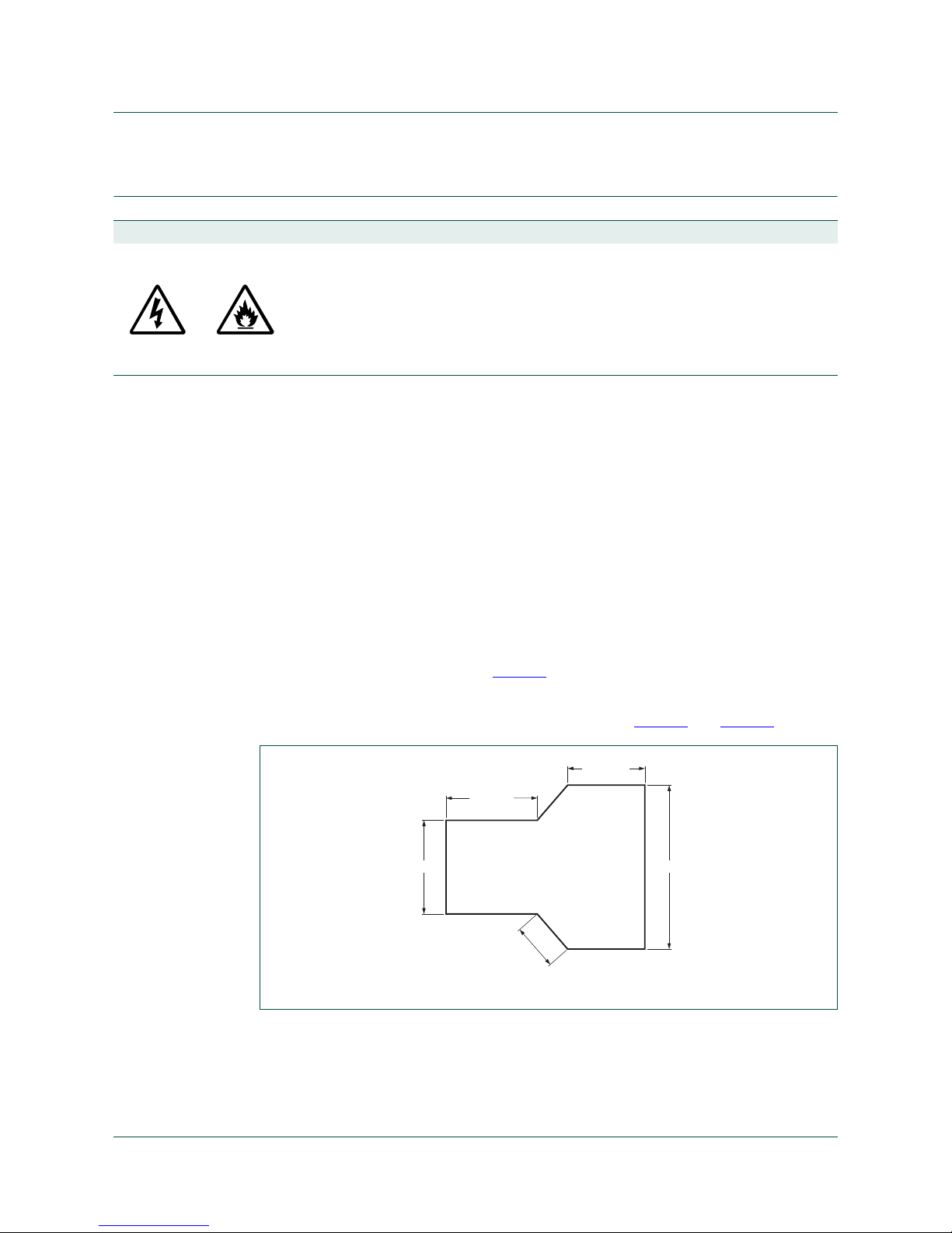
The board dimensions are shown in Figure 1
. The board is designed with the components
allowing enough headroom when the board is inserted into a GU10 lamp base.
The assembled top and bottom board views are shown in Figure 2
and Figure 3.
WARNING
Lethal voltage and fire ignition hazard
The non-insulated high voltages that are present when operating this product, constitute a
risk of electric shock, personal injury, death and/or ignition of fire.
This product is intended for evaluation purposes only. It shall be operated in a designated test
area by personnel qualified according to local requirements and labor laws to work with
non-insulated mains voltages and high-voltage circuits. This product shall never be operated
unattended.
Fig 1. Dimensions of the reference board
aaa-002431
18 mm
30.8 mm
18.1 mm
8.7 mm
15.3 mm
Page 4

UM10516 All information provided in this document is subject to legal disclaimers. © NXP B.V. 2012. All rights reserved.
User manual Rev. 1 — 27 March 2012 4 of 16
NXP Semiconductors
UM10516
230 V 7 W GU10 buck converter SSL2101 reference board
Fig 2. Reference board (top view)
Fig 3. Reference board (bottom view)
Page 5

UM10516 All information provided in this document is subject to legal disclaimers. © NXP B.V. 2012. All rights reserved.
User manual Rev. 1 — 27 March 2012 5 of 16
NXP Semiconductors
UM10516
230 V 7 W GU10 buck converter SSL2101 reference board
2. Safety warning
This board is connected to the mains voltage. Avoid touching the board while it is
connected to the mains voltage. An isolated housing is obligatory when used in
uncontrolled, non-laboratory environments. Galvanic isolation o f the ma ins phase usin g a
variable transformer is always recommended.
3. Specifications
a. Isolated b. Non-isolated
Fig 4. Variable transformer (Variac) isolation symbols
019aab173
019aab174
Table 1. Specifications for the reference board
Symbol Parameter Value
V
mains
AC mains supply voltage 230 V
V
LED
DC output voltage 15.6 V
I
LED
output current 415 mA
I
o
/V
o
output voltage rejection 2 mA/V
efficiency 76 %
PF Power Factor 0.9
f
sw
switching frequency 85 kHz
Page 6

UM10516 All information provided in this document is subject to legal disclaimers. © NXP B.V. 2012. All rights reserved.
User manual Rev. 1 — 27 March 2012 6 of 16
NXP Semiconductors
UM10516
230 V 7 W GU10 buck converter SSL2101 reference board
4. Functional description
4.1 General
The 230 V, 7 W buck reference board uses the SSL2101 con trol IC to drive a load of up to
5-LEDs. The SSL2101 is a Switched Mode Power Supply (SMPS) controller with an
integrated MOSFET. Detailed information about the SSL2 101 operation is contained in the
SSL2101 SMPS IC for dimmable LED lighting data sheet.
The converter operates in Discontinuous Conduction Mode (DCM) or Boundary
Conduction Mode (BCM). In BCM, valley switching detection is used to minimize magnetic
component and switching losses while enhancing efficiency . A valley-fill circuit is added to
obtain high-power factor.
The reference board is triac dimmable and can be used in combination with most leading
and trailing edge dimmers. During dimming, the rectified mains voltage is averaged and
attenuated and supplied to both BRIGHTNESS and PWMLIMIT pins of the SSL2101. As a
consequence, the converter duty cycle or frequency is reduced and as a result the LED
output current.
Dimming compatibility is defined as smooth dimming without any flashing artifacts across
the complete dimming range. This reference board provides a dimming compatibility of
> 85 % when tested with a current selection of 30 trailing and leading-edge dimmers.
5. Reference board connections
The GU10 LED driver board takes a 230 V, 50 Hz mains supply and supports a 5-LED
load.
Remark: Make all connections with the input power is switched off.
• Connect the 5-LED load as output load together with power meter at both inputs and
outputs.
• Connect V
IN
(230 V/50 Hz) using an isolating transformer to the input connection
points of the buck converter. Alternatively use an AC power supply with limited output
current capability (for example; 200 mA).
• Increase V
IN
to 230 V and measure the different parameters as shown in Table 2.
• When testing dimmer compatibility, connect a leading or trailing edge dimmer
between V
IN
and the buck converter input connection points.
Remark: Use protective a shield over application and never touch the board when
measuring or testing.
Table 2. Input and output parameters
VIN (V) II (mA) PF P (W) V
O
I
O
P
O
(%)
230 41 0.9 8.5 15.6 415 6.5 0.76
Page 7

UM10516 All information provided in this document is subject to legal disclaimers. © NXP B.V. 2012. All rights reserved.
User manual Rev. 1 — 27 March 2012 7 of 16
NXP Semiconductors
UM10516
230 V 7 W GU10 buck converter SSL2101 reference board
Remark: Make all connections with the input power is switched off.
Remark: The board in Figure 5
shows the GU10 subboard. The connections can also be
made to the outer (main) board.
Fig 5. Connection to the reference board
Fig 6. Connection to the reference board
aaa-002434
amp
meter
volt
meter
l
I
V
IN
5-LED string
A
A
V
V
volt
meter
amp
meter
Page 8

UM10516 All information provided in this document is subject to legal disclaimers. © NXP B.V. 2012. All rights reserved.
User manual Rev. 1 — 27 March 2012 8 of 16
NXP Semiconductors
UM10516
230 V 7 W GU10 buck converter SSL2101 reference board
6. Performance data
The performance was measured with 5 LEDs connected as output load. The performance
data is shown in Figure 7
to Figure 10.
6.1 Efficiency
6.2 Output current
Fig 7. Efficiency as a function of AC mains input voltage
50
80
70
60
90
efficiency
(%)
V
IN
(V)
205 255245225 235215
aaa-002436
Fig 8. Output current as a function of AC mains input voltage
412
416
408
420
424
I
out
(mA)
404
V
IN
(V)
205 255245225 235215
aaa-002441
Page 9

UM10516 All information provided in this document is subject to legal disclaimers. © NXP B.V. 2012. All rights reserved.
User manual Rev. 1 — 27 March 2012 9 of 16
NXP Semiconductors
UM10516
230 V 7 W GU10 buck converter SSL2101 reference board
6.3 Power factor
6.4 Output voltage rejection
Fig 9. Power factor as a function of AC mains input voltage
0.6
0.9
0.8
0.7
1.0
PF
V
IN
(V)
205 255245225 235215
aaa-002442
Fig 10. Output current as a function of Output voltage
200
300
100
400
500
I
I
(mA)
0
V
O
(V)
11 211915 1713
aaa-002443
Page 10

UM10516 All information provided in this document is subject to legal disclaimers. © NXP B.V. 2012. All rights reserved.
User manual Rev. 1 — 27 March 2012 10 of 16
NXP Semiconductors
UM10516
230 V 7 W GU10 buck converter SSL2101 reference board
6.5 ElectroMagnetic Interference (EMI)
6.6 Weighted audible noise
Fig 11. EMI: L and N phases
Fig 12. Weighted audible noise as a function of frequency
-120
0
-40
-80
40
(dBA)
f (kHz)
0 250002000010000 150005000
aaa-002445
Page 11

UM10516 All information provided in this document is subject to legal disclaimers. © NXP B.V. 2012. All rights reserved.
User manual Rev. 1 — 27 March 2012 11 of 16
NXP Semiconductors
UM10516
230 V 7 W GU10 buck converter SSL2101 reference board
7. Schematic
Fig 13. Schematic diagram: 230 V 7 W buck converter using the SSL2101
aaa-002446
U
SBLEED
WBLEED
VCC
VCC
GND
GND
BRIGHTNESS
RC2
RC
DRAIN
GND
GND
GND
SOURCE
R12
C8
330 pF
25 V
C7
4.7 μF
25 V
C1
100 nF
450 V
C3
3.3 μF
200 V
C2
3.3 μF
200 V
C4
220 nF
450 V
C6
4.7 μF
50 V
C9
330 pF
25 V
T1
T6592
C5
470 μF
25 V
5 LEDs
415 mA
+
-
6
5
2
3
D5
ES1G-13-F
R10
7.5 kΩ
R9
30 kΩ
R5
220 kΩ
R4
4.7 kΩ
R6
Q1
ZTX558
22 kΩ
R3
D1
US1G-13-F
D3
SIG-13-F
D4
SIG-13-F
D6
ES1F
D7
BZV55-C15
D2
SIG-13-F
100 kΩ
L1
680 μH
R1
MOV1
160 Ω
R2
160 Ω
L
N
230 V
50 Hz
R11
100 kΩ
R8
8.2 kΩ
R7
604 kΩ
RGND
RGND
RGND
BD1
B6S-G
C10
33 nF
630 V
X2 class
D8
BZV55-B75
0.68 Ω
AUX
ISENSE
PWMLIMIT
VCC
1
2
3
4
5
6
7
8
16
15
14
13
12
11
10
9
U1
SSL2101
R13
R14
10 Ω
R16
20 kΩ
100 kΩ
R15
4.1 kΩ
R17
10 Ω
Page 12

UM10516 All information provided in this document is subject to legal disclaimers. © NXP B.V. 2012. All rights reserved.
User manual Rev. 1 — 27 March 2012 12 of 16
NXP Semiconductors
UM10516
230 V 7 W GU10 buck converter SSL2101 reference board
8. Bill of materials
Table 3. Bill of materials
Part reference Description/value Manufacturer/part number
BD1 bridge rectifi er; 600 V, 0.8 A Comchip Technology; B6S-G
C1 0.1 F; 450 V (DC); 10 %; epoxy coated
ceramic; radial
Murata; RDED72W104K3K1
C2, C3 3.3 F; 200 V; electrolytic; radial Nichicon; UVZ2D3R3MED
C4 0.22 F; 450 V (DC); 10 %; epoxy coated
ceramic; radial
Murata; RDED72W224K5E1
C5 470 F; 25 V; 20 %; electro lytic; radial Panasonic - ECG; ECA-1EM471B
C6 4.7 F; 50 V; 10 %; X5R ceramic; 1206 Taiyo Yuden; UMK316BJ475KL-T
C7 4.7 F; 25 V; 20 %; X7R ceramic; 1206 TDK; C3216X7R1E475M
C8, C9 330 pF; 25 V; 5 %; COG (NPO); 0603 AVX; 06033A331JAT2A
C10 0.033 F; 305 V (AC); 630 V (DC); 20 %;
X2 class; radial
EPCOS; B32921C3333M; long lead
D1 fast diode; 400 V; 1 A; DO214AC Diodes Inc.; US1G-13-F
D2, D3, D4 fast diodes; 400 V; 1 A; DO214AC Diodes Inc.; S1G-13-F
D5 fast diode; 400 V; 1 A; DO214AC Diodes Inc.; ES1G-13-F
D6 fast diode; 300 V; 1 A; DO214AC Fairchild; ES1F
D7 Zener diode; 15 V; 500 mW; SOD80 NXP; BZ V55-C15,135
D8 Zener diode; 75 V; 500 mW; SOD80 NXP; BZV55-B75,115
J1 wire-connection; 0.6 mm J2 wire-connection; 0.6 mm J3 wire-connection; 0.6 mm J4 wire-connection; 0.6 mm J5 receptacle 2.54 mm; single 6-way SAMTEC; SSW-106-02-G-S-RA
J6 MKDSN 2.5/ 2-5.08 PHOENIX CONTACT; 1888687
L1 680 H; 160 mA; (L W H = 7 7 3.2 mm) Bourns Inc.; SRR7032-681M
MOV1 transient/surge absorber; 470 V Panasonic - ECG; ERZ-V07D471
Q1 MOSFET PNP 400 V; 200 mA TO92-3 Diodes/Zetex; ZTX558
R1, R2 160 ; 0.25 W; 5 %; axial Panasonic - ECG; ERD-S2TJ161V
R3 100 k; 0.25 W; 5 %; axial Panasonic - ECG; ERD-S2TJ104V
R4 4.7 k; 0.1 W; 5 %; 0603 Panasonic - ECG; ERJ-3GEYJ472V
R5 220 k; 0.25 W; 5 %; axial Panasonic - ECG; ERD-S2TJ224V
R6 22 k; 2 W; 5 %; axial Vishay; PR02000202002JR500
R7 604 k; 0.25 W; 1 %; 1206 Vishay; PR02000202202JR500
R8 8.2 k, 0.1 W; 5 %; 0603 Vishay; CRCW1206604KFKEA
R9 30 k; 0.1 W; 5 %; 0603 Multicomp; MC 0.063W 0603 8K2
R10 7.5 k; 0.1 W; 5 %; 0603 Vishay; CRCW060330K0FKEA
R11, R13 100 k; 0.1 W; 5 %; 0603 YAGEO; RC0603JR-077K5L
R12 680 m; 0.2 5 W; 1 %; 1206 Bourns; CR0603-JW-104GLF
R14 10 ; 0.1 W; 5 %; 0603 Multicomp; MC1206W4F680LT5E
Page 13

UM10516 All information provided in this document is subject to legal disclaimers. © NXP B.V. 2012. All rights reserved.
User manual Rev. 1 — 27 March 2012 13 of 16
NXP Semiconductors
UM10516
230 V 7 W GU10 buck converter SSL2101 reference board
9. PCB layout
R15 4.1 k; 0.1 W; 1 %; 0603 Multicomp; MC0603SAF4121T5E
R16 20 k; 0.1 W; 1 %; 0603 Bourns; CR0603-JW-203GLF
R17 10 ; 0.25 W; 1 %; 0805 Bourns; CR0603-JW-100GLF
T1 L
pri
= 180 H; N
pri:Nsec
= 1.35 : 1 EPCOS; T6592
U1 SMPS controller IC for driving LED applications;
SO16
NXP Semiconductor; SSL2101T
Table 3. Bill of materials …continued
Part reference Description/value Manufacturer/part number
a. Top layer b. Bottom layer -
Fig 14. Board layout
Page 14

UM10516 All information provided in this document is subject to legal disclaimers. © NXP B.V. 2012. All rights reserved.
User manual Rev. 1 — 27 March 2012 14 of 16
NXP Semiconductors
UM10516
230 V 7 W GU10 buck converter SSL2101 reference board
10. Inductor specification
Fig 15. Inductor specification
Table 4. Electrical specification
All values are specified at 25
C unless otherwise specified. All values without tolerances are typical
values.
Parameter Value Comment
Inductance 2 to 3 180 H, 7% 100mV, 10kHz
Inductance 2 to 3 143 H minimum 100 mV, 10 kHz; 1 A (DC)
DCR 2 to 3 380 m maximum At 25
C
DCR 6 to 5 830 m maximum At 25 C
Turns Ratio 2to3:6to5 1.35:1
HV 2 to 5 500 V 50/60Hz, 2 mA maximum,
2 s minimum
Leakage Inductance 2 to 3 12 H maximum with 5 to 6 shorted; 100 mV,
100 kHz
aaa-002449
10.1 max
1
2.54 mm
2
2
3
6
5
EPCOS
T659
.YYWW
10.1 max
5
3
2
6
11.0 max
Marking:
Dimensions [mm]: Schematics:
YYWW means:
EPCOS
T6592
YYWW
Date code Year and Week
3.25
1
3
R0.5
5
Page 15

UM10516 All information provided in this document is subject to legal disclaimers. © NXP B.V. 2012. All rights reserved.
User manual Rev. 1 — 27 March 2012 15 of 16
NXP Semiconductors
UM10516
230 V 7 W GU10 buck converter SSL2101 reference board
11. Legal information
11.1 Definitions
Draft — The document is a draft version only. The content is still under
internal review and subject to formal approval, which may result in
modifications or additions. NXP Semiconductors does not give any
representations or warranties as to the accuracy or completeness of
information included herein and shall have no liability for the consequences of
use of such information.
11.2 Disclaimers
Limited warranty and liability — Information in this document is believed to
be accurate and reliable. However, NXP Semiconductors does not give any
representations or warranties, expressed or implied, as to the accuracy or
completeness of such information and shall have no liability for the
consequences of use of such information. NXP Semiconductors takes no
responsibility for the content in this document if provided by an information
source outside of NXP Semiconductors.
In no event shall NXP Semiconductors be liable fo r any indirect, incidental,
punitive, special or consequential damages (including - without limitation - lost
profits, lost savings, business interruption, costs related to the removal or
replacement of any products or rework charges) whether or not such
damages are based on tort (including negligence), warranty, breach of
contract or any other legal theory.
Notwithstanding any damages that customer might incur for any reason
whatsoever, NXP Semico nductors’ aggregate and cumulative liabili ty towards
customer for the products described herein shall be limited in accordance
with the Terms and conditions of commercial sale of NXP Semiconductors.
Right to make changes — NXP Semiconductors reserves the right to make
changes to information published in this document, including without
limitation specifications and product descriptions, at any time and without
notice. This document supersedes and replaces all information supplied prior
to the publication hereof.
Suitability for use — NXP Semiconductors products are not designed,
authorized or warranted to be suitable for use in life support, life-critical or
safety-critical systems or equipment, nor in applications where failure or
malfunction of an NXP Semiconductors product can reasonably be expected
to result in personal injury, death or severe property or environmental
damage. NXP Semiconductors and its suppliers accept no liability for
inclusion and/or use of NXP Semiconductors products in such equipment or
applications and therefore such inclusion and/or use is at the cust omer’s own
risk.
Applications — Applications that are described herein for any of these
products are for illustrative purposes only. NXP Semiconductors makes no
representation or warranty that such applications will be suitable for the
specified use without further testing or modification.
Customers are responsible for the design and operation of their applications
and products using NXP Semiconductors products, and NXP Semi conductors
accepts no liability for any assistance with applications or customer product
design. It is customer’s sole responsibility to determine whether the NXP
Semiconductors product is suitable and fit for the customer’s applications and
products planned, as well as for the planned application and use of
customer’s third party customer(s). Customers should provide appropriate
design and operating safeguards to minimize the risks associated with their
applications and products.
NXP Semiconductors does not accept any liability related to any default,
damage, costs or problem which is based on any weakness or default in the
customer’s applications or products, or the application or use by customer’s
third party customer(s). Customer is responsible for doing all necessary
testing for the customer’s applications and products using NXP
Semiconductors products in order to avoid a default of the applications and
the products or of the application or use by customer’s third party
customer(s). NXP does not accept any liability in this respect.
Export control — This document as well as the item(s) described herein
may be subject to export control regulations. Export might require a prior
authorization from competent authorities.
Evaluation products — This product is provided on an “as is” and “with all
faults” basis for evaluation purposes only. NXP Semiconductors, its affiliates
and their suppliers expressly disclaim all warranties, whether express, implied
or statutory, including but not limited to the implied warranties of
non-infringement, merchantability and fitness for a particular purpose. The
entire risk as to the quality, or arising out of the use or performance, of this
product remains with customer.
In no event shall NXP Semiconductors, its affiliates or their supplie rs be liable
to customer for any special, indirect, consequential, punitive or incidental
damages (including without limitation damages for l oss of busi ness, busi ness
interruption, loss of use, loss of data or information, and the like) arising out
the use of or inability to use the product, whether or not based on tort
(including negligence), strict liability, breach of contract, breach of warranty or
any other theory, even if advised of the possibility of such damages.
Notwithstanding any damages that customer might incur for any reason
whatsoever (including without limitation, all damages referenced above and
all direct or general damages), the entire liability of NXP Semiconductors, its
affiliates and their suppliers and customer’s exclusive remedy for all of the
foregoing shall be limited to actual damages incurred by customer based on
reasonable reliance up to the greater of the amount actually paid by customer
for the product or five dollars (US$5.00). The foregoin g limitations, e xclusions
and disclaimers shall apply to the maximum extent permitted by applicable
law, even if any remedy fails of its essential purpose.
11.3 Trademarks
Notice: All referenced brands, prod uct names, service names and trademarks
are the property of their respective owners.
Page 16

NXP Semiconductors
UM10516
230 V 7 W GU10 buck converter SSL2101 reference board
© NXP B.V. 2012. All rights reserved.
For more information, please visit: http://www.nxp.com
For sales office addresses, please send an email to: salesaddresses@nxp.com
Date of release: 27 March 2012
Document identifier: UM10516
Please be aware that important notices concerning this document and the product(s)
described herein, have been included in section ‘Legal information’.
12. Contents
1 Introduction . . . . . . . . . . . . . . . . . . . . . . . . . . . . 3
2 Safety warning . . . . . . . . . . . . . . . . . . . . . . . . . . 5
3 Specifications. . . . . . . . . . . . . . . . . . . . . . . . . . . 5
4 Functional description . . . . . . . . . . . . . . . . . . . 6
4.1 General. . . . . . . . . . . . . . . . . . . . . . . . . . . . . . . 6
5 Reference board connections . . . . . . . . . . . . . 6
6 Performance data. . . . . . . . . . . . . . . . . . . . . . . . 8
6.1 Efficiency . . . . . . . . . . . . . . . . . . . . . . . . . . . . . 8
6.2 Output current. . . . . . . . . . . . . . . . . . . . . . . . . . 8
6.3 Power factor . . . . . . . . . . . . . . . . . . . . . . . . . . . 9
6.4 Output voltage rejection . . . . . . . . . . . . . . . . . . 9
6.5 ElectroMagnetic Interference (EMI) . . . . . . . . 10
6.6 Weighted audible noise . . . . . . . . . . . . . . . . . 10
7 Schematic. . . . . . . . . . . . . . . . . . . . . . . . . . . . . 11
8 Bill of materials . . . . . . . . . . . . . . . . . . . . . . . . 12
9 PCB layout . . . . . . . . . . . . . . . . . . . . . . . . . . . . 13
10 Inductor specification . . . . . . . . . . . . . . . . . . . 14
11 Legal information. . . . . . . . . . . . . . . . . . . . . . . 15
11.1 Definitions. . . . . . . . . . . . . . . . . . . . . . . . . . . . 15
11.2 Disclaimers. . . . . . . . . . . . . . . . . . . . . . . . . . . 15
11.3 Trademarks. . . . . . . . . . . . . . . . . . . . . . . . . . . 15
12 Contents . . . . . . . . . . . . . . . . . . . . . . . . . . . . . . 16
Page 17

Компания «ЭлектроПласт» предлагает заключение долгосрочных отношений при
поставках импортных электронных компонентов на взаимовыгодных условиях!
Наши преимущества:
Оперативные поставки широкого спектра электронных компонентов отечественного и
импортного производства напрямую от производителей и с крупнейших мировых
складов;
Поставка более 17-ти миллионов наименований электронных компонентов;
Поставка сложных, дефицитных, либо снятых с производства позиций;
Оперативные сроки поставки под заказ (от 5 рабочих дней);
Экспресс доставка в любую точку России;
Техническая поддержка проекта, помощь в подборе аналогов, поставка прототипов;
Система менеджмента качества сертифицирована по Международному стандарту ISO
9001;
Лицензия ФСБ на осуществление работ с использованием сведений, составляющих
государственную тайну;
Поставка специализированных компонентов (Xilinx, Altera, Analog Devices, Intersil,
Interpoint, Microsemi, Aeroflex, Peregrine, Syfer, Eurofarad, Texas Instrument, Miteq,
Cobham, E2V, MA-COM, Hittite, Mini-Circuits,General Dynamics и др.);
Помимо этого, одним из направлений компании «ЭлектроПласт» является направление
«Источники питания». Мы предлагаем Вам помощь Конструкторского отдела:
Подбор оптимального решения, техническое обоснование при выборе компонента;
Подбор аналогов;
Консультации по применению компонента;
Поставка образцов и прототипов;
Техническая поддержка проекта;
Защита от снятия компонента с производства.
Как с нами связаться
Телефон: 8 (812) 309 58 32 (многоканальный)
Факс: 8 (812) 320-02-42
Электронная почта: org@eplast1.ru
Адрес: 198099, г. Санкт-Петербург, ул. Калинина,
дом 2, корпус 4, литера А.
 Loading...